EP2087516B1 - Fabrication au niveau de la plaquette de puces à couvercle comportant une couche diélectrique appliquée par électrodéposition - Google Patents
Fabrication au niveau de la plaquette de puces à couvercle comportant une couche diélectrique appliquée par électrodéposition Download PDFInfo
- Publication number
- EP2087516B1 EP2087516B1 EP07852914.6A EP07852914A EP2087516B1 EP 2087516 B1 EP2087516 B1 EP 2087516B1 EP 07852914 A EP07852914 A EP 07852914A EP 2087516 B1 EP2087516 B1 EP 2087516B1
- Authority
- EP
- European Patent Office
- Prior art keywords
- conductive
- conductive traces
- layer
- semiconductor chip
- contacts
- Prior art date
- Legal status (The legal status is an assumption and is not a legal conclusion. Google has not performed a legal analysis and makes no representation as to the accuracy of the status listed.)
- Active
Links
- 238000004519 manufacturing process Methods 0.000 title claims description 22
- 239000011248 coating agent Substances 0.000 title description 60
- 238000000576 coating method Methods 0.000 title description 60
- 239000004065 semiconductor Substances 0.000 claims description 143
- 238000000034 method Methods 0.000 claims description 50
- 239000000463 material Substances 0.000 claims description 36
- 238000004377 microelectronic Methods 0.000 claims description 26
- 238000000151 deposition Methods 0.000 claims description 20
- 238000004891 communication Methods 0.000 claims description 10
- 230000002093 peripheral effect Effects 0.000 claims description 8
- 230000001154 acute effect Effects 0.000 claims 2
- 229910052751 metal Inorganic materials 0.000 description 78
- 239000002184 metal Substances 0.000 description 78
- 235000012431 wafers Nutrition 0.000 description 38
- 239000004020 conductor Substances 0.000 description 31
- 230000008569 process Effects 0.000 description 27
- 230000003287 optical effect Effects 0.000 description 21
- 238000002161 passivation Methods 0.000 description 21
- 238000003384 imaging method Methods 0.000 description 20
- 238000001652 electrophoretic deposition Methods 0.000 description 18
- 239000003989 dielectric material Substances 0.000 description 15
- 230000008021 deposition Effects 0.000 description 14
- 238000012545 processing Methods 0.000 description 13
- 229910000679 solder Inorganic materials 0.000 description 13
- PXHVJJICTQNCMI-UHFFFAOYSA-N Nickel Chemical compound [Ni] PXHVJJICTQNCMI-UHFFFAOYSA-N 0.000 description 8
- 238000000059 patterning Methods 0.000 description 8
- RYGMFSIKBFXOCR-UHFFFAOYSA-N Copper Chemical compound [Cu] RYGMFSIKBFXOCR-UHFFFAOYSA-N 0.000 description 7
- 239000004593 Epoxy Substances 0.000 description 7
- 229910052802 copper Inorganic materials 0.000 description 7
- 239000010949 copper Substances 0.000 description 7
- 238000005530 etching Methods 0.000 description 7
- 230000000873 masking effect Effects 0.000 description 6
- 239000007787 solid Substances 0.000 description 6
- 239000000758 substrate Substances 0.000 description 6
- 230000007704 transition Effects 0.000 description 6
- 238000004140 cleaning Methods 0.000 description 5
- 238000009713 electroplating Methods 0.000 description 5
- 230000036961 partial effect Effects 0.000 description 5
- 229920000642 polymer Polymers 0.000 description 5
- 238000004544 sputter deposition Methods 0.000 description 5
- 238000012360 testing method Methods 0.000 description 5
- VYPSYNLAJGMNEJ-UHFFFAOYSA-N Silicium dioxide Chemical compound O=[Si]=O VYPSYNLAJGMNEJ-UHFFFAOYSA-N 0.000 description 4
- ATJFFYVFTNAWJD-UHFFFAOYSA-N Tin Chemical compound [Sn] ATJFFYVFTNAWJD-UHFFFAOYSA-N 0.000 description 4
- 239000000853 adhesive Substances 0.000 description 4
- 230000001070 adhesive effect Effects 0.000 description 4
- 230000005684 electric field Effects 0.000 description 4
- 150000002739 metals Chemical class 0.000 description 4
- 229910052759 nickel Inorganic materials 0.000 description 4
- 229910000510 noble metal Inorganic materials 0.000 description 4
- 238000004806 packaging method and process Methods 0.000 description 4
- 238000004528 spin coating Methods 0.000 description 4
- XUIMIQQOPSSXEZ-UHFFFAOYSA-N Silicon Chemical compound [Si] XUIMIQQOPSSXEZ-UHFFFAOYSA-N 0.000 description 3
- RTAQQCXQSZGOHL-UHFFFAOYSA-N Titanium Chemical compound [Ti] RTAQQCXQSZGOHL-UHFFFAOYSA-N 0.000 description 3
- 229910052782 aluminium Inorganic materials 0.000 description 3
- XAGFODPZIPBFFR-UHFFFAOYSA-N aluminium Chemical compound [Al] XAGFODPZIPBFFR-UHFFFAOYSA-N 0.000 description 3
- 230000005540 biological transmission Effects 0.000 description 3
- 230000005496 eutectics Effects 0.000 description 3
- 239000012530 fluid Substances 0.000 description 3
- 238000002955 isolation Methods 0.000 description 3
- 230000013011 mating Effects 0.000 description 3
- 230000008018 melting Effects 0.000 description 3
- 238000002844 melting Methods 0.000 description 3
- 239000000203 mixture Substances 0.000 description 3
- 238000007747 plating Methods 0.000 description 3
- 239000002243 precursor Substances 0.000 description 3
- 229910052710 silicon Inorganic materials 0.000 description 3
- 239000010703 silicon Substances 0.000 description 3
- 239000010936 titanium Substances 0.000 description 3
- 229910052719 titanium Inorganic materials 0.000 description 3
- 238000007740 vapor deposition Methods 0.000 description 3
- KDLHZDBZIXYQEI-UHFFFAOYSA-N Palladium Chemical compound [Pd] KDLHZDBZIXYQEI-UHFFFAOYSA-N 0.000 description 2
- 229910052581 Si3N4 Inorganic materials 0.000 description 2
- 239000000654 additive Substances 0.000 description 2
- 230000000996 additive effect Effects 0.000 description 2
- 239000006117 anti-reflective coating Substances 0.000 description 2
- 230000015572 biosynthetic process Effects 0.000 description 2
- 239000000356 contaminant Substances 0.000 description 2
- 238000011109 contamination Methods 0.000 description 2
- 238000010586 diagram Methods 0.000 description 2
- 238000005553 drilling Methods 0.000 description 2
- -1 e.g. Substances 0.000 description 2
- 230000006870 function Effects 0.000 description 2
- 239000011521 glass Substances 0.000 description 2
- 238000010438 heat treatment Methods 0.000 description 2
- 238000009413 insulation Methods 0.000 description 2
- 239000011368 organic material Substances 0.000 description 2
- 238000012858 packaging process Methods 0.000 description 2
- 238000000206 photolithography Methods 0.000 description 2
- 229920002120 photoresistant polymer Polymers 0.000 description 2
- BASFCYQUMIYNBI-UHFFFAOYSA-N platinum Chemical compound [Pt] BASFCYQUMIYNBI-UHFFFAOYSA-N 0.000 description 2
- 229920002635 polyurethane Polymers 0.000 description 2
- 239000004814 polyurethane Substances 0.000 description 2
- 230000002829 reductive effect Effects 0.000 description 2
- 235000012239 silicon dioxide Nutrition 0.000 description 2
- 239000000377 silicon dioxide Substances 0.000 description 2
- HQVNEWCFYHHQES-UHFFFAOYSA-N silicon nitride Chemical compound N12[Si]34N5[Si]62N3[Si]51N64 HQVNEWCFYHHQES-UHFFFAOYSA-N 0.000 description 2
- 239000007779 soft material Substances 0.000 description 2
- 238000001228 spectrum Methods 0.000 description 2
- 238000009718 spray deposition Methods 0.000 description 2
- 238000005507 spraying Methods 0.000 description 2
- 230000035882 stress Effects 0.000 description 2
- XLYOFNOQVPJJNP-UHFFFAOYSA-N water Substances O XLYOFNOQVPJJNP-UHFFFAOYSA-N 0.000 description 2
- XVEUJTIZHZIHJM-UHFFFAOYSA-N a828782 Chemical compound CCOC(N)=O.CCOC(N)=O XVEUJTIZHZIHJM-UHFFFAOYSA-N 0.000 description 1
- NIXOWILDQLNWCW-UHFFFAOYSA-N acrylic acid group Chemical group C(C=C)(=O)O NIXOWILDQLNWCW-UHFFFAOYSA-N 0.000 description 1
- 229920006397 acrylic thermoplastic Polymers 0.000 description 1
- 230000008901 benefit Effects 0.000 description 1
- 239000003990 capacitor Substances 0.000 description 1
- 230000008859 change Effects 0.000 description 1
- 238000006243 chemical reaction Methods 0.000 description 1
- 230000007797 corrosion Effects 0.000 description 1
- 238000005260 corrosion Methods 0.000 description 1
- 230000007423 decrease Effects 0.000 description 1
- 230000003247 decreasing effect Effects 0.000 description 1
- 238000009792 diffusion process Methods 0.000 description 1
- 238000004090 dissolution Methods 0.000 description 1
- 238000009826 distribution Methods 0.000 description 1
- 239000000428 dust Substances 0.000 description 1
- 230000000694 effects Effects 0.000 description 1
- 238000004070 electrodeposition Methods 0.000 description 1
- 238000007772 electroless plating Methods 0.000 description 1
- 230000005670 electromagnetic radiation Effects 0.000 description 1
- 239000008393 encapsulating agent Substances 0.000 description 1
- 239000000374 eutectic mixture Substances 0.000 description 1
- 230000002349 favourable effect Effects 0.000 description 1
- PCHJSUWPFVWCPO-UHFFFAOYSA-N gold Chemical compound [Au] PCHJSUWPFVWCPO-UHFFFAOYSA-N 0.000 description 1
- 229910052737 gold Inorganic materials 0.000 description 1
- 239000010931 gold Substances 0.000 description 1
- 238000000227 grinding Methods 0.000 description 1
- 239000011147 inorganic material Substances 0.000 description 1
- 238000005304 joining Methods 0.000 description 1
- 230000000670 limiting effect Effects 0.000 description 1
- 239000007788 liquid Substances 0.000 description 1
- 238000010297 mechanical methods and process Methods 0.000 description 1
- 230000005226 mechanical processes and functions Effects 0.000 description 1
- 230000015654 memory Effects 0.000 description 1
- 238000001465 metallisation Methods 0.000 description 1
- 238000012986 modification Methods 0.000 description 1
- 230000004048 modification Effects 0.000 description 1
- 230000005693 optoelectronics Effects 0.000 description 1
- 229910052763 palladium Inorganic materials 0.000 description 1
- 239000002245 particle Substances 0.000 description 1
- 238000001020 plasma etching Methods 0.000 description 1
- 229910052697 platinum Inorganic materials 0.000 description 1
- 229920003229 poly(methyl methacrylate) Polymers 0.000 description 1
- 229920001296 polysiloxane Polymers 0.000 description 1
- 230000004044 response Effects 0.000 description 1
- 238000007761 roller coating Methods 0.000 description 1
- 230000008054 signal transmission Effects 0.000 description 1
- 239000002904 solvent Substances 0.000 description 1
- 239000000126 substance Substances 0.000 description 1
- ISXSCDLOGDJUNJ-UHFFFAOYSA-N tert-butyl prop-2-enoate Chemical compound CC(C)(C)OC(=O)C=C ISXSCDLOGDJUNJ-UHFFFAOYSA-N 0.000 description 1
- 230000008646 thermal stress Effects 0.000 description 1
- 238000012546 transfer Methods 0.000 description 1
Images


Classifications
-
- H—ELECTRICITY
- H10—SEMICONDUCTOR DEVICES; ELECTRIC SOLID-STATE DEVICES NOT OTHERWISE PROVIDED FOR
- H10K—ORGANIC ELECTRIC SOLID-STATE DEVICES
- H10K19/00—Integrated devices, or assemblies of multiple devices, comprising at least one organic element specially adapted for rectifying, amplifying, oscillating or switching, covered by group H10K10/00
-
- H—ELECTRICITY
- H01—ELECTRIC ELEMENTS
- H01L—SEMICONDUCTOR DEVICES NOT COVERED BY CLASS H10
- H01L23/00—Details of semiconductor or other solid state devices
- H01L23/28—Encapsulations, e.g. encapsulating layers, coatings, e.g. for protection
- H01L23/31—Encapsulations, e.g. encapsulating layers, coatings, e.g. for protection characterised by the arrangement or shape
- H01L23/3107—Encapsulations, e.g. encapsulating layers, coatings, e.g. for protection characterised by the arrangement or shape the device being completely enclosed
- H01L23/3114—Encapsulations, e.g. encapsulating layers, coatings, e.g. for protection characterised by the arrangement or shape the device being completely enclosed the device being a chip scale package, e.g. CSP
-
- H—ELECTRICITY
- H01—ELECTRIC ELEMENTS
- H01L—SEMICONDUCTOR DEVICES NOT COVERED BY CLASS H10
- H01L21/00—Processes or apparatus adapted for the manufacture or treatment of semiconductor or solid state devices or of parts thereof
- H01L21/67—Apparatus specially adapted for handling semiconductor or electric solid state devices during manufacture or treatment thereof; Apparatus specially adapted for handling wafers during manufacture or treatment of semiconductor or electric solid state devices or components ; Apparatus not specifically provided for elsewhere
- H01L21/683—Apparatus specially adapted for handling semiconductor or electric solid state devices during manufacture or treatment thereof; Apparatus specially adapted for handling wafers during manufacture or treatment of semiconductor or electric solid state devices or components ; Apparatus not specifically provided for elsewhere for supporting or gripping
- H01L21/6835—Apparatus specially adapted for handling semiconductor or electric solid state devices during manufacture or treatment thereof; Apparatus specially adapted for handling wafers during manufacture or treatment of semiconductor or electric solid state devices or components ; Apparatus not specifically provided for elsewhere for supporting or gripping using temporarily an auxiliary support
- H01L21/6836—Wafer tapes, e.g. grinding or dicing support tapes
-
- H—ELECTRICITY
- H01—ELECTRIC ELEMENTS
- H01L—SEMICONDUCTOR DEVICES NOT COVERED BY CLASS H10
- H01L23/00—Details of semiconductor or other solid state devices
- H01L23/28—Encapsulations, e.g. encapsulating layers, coatings, e.g. for protection
- H01L23/31—Encapsulations, e.g. encapsulating layers, coatings, e.g. for protection characterised by the arrangement or shape
-
- H—ELECTRICITY
- H01—ELECTRIC ELEMENTS
- H01L—SEMICONDUCTOR DEVICES NOT COVERED BY CLASS H10
- H01L23/00—Details of semiconductor or other solid state devices
- H01L23/48—Arrangements for conducting electric current to or from the solid state body in operation, e.g. leads, terminal arrangements ; Selection of materials therefor
- H01L23/481—Internal lead connections, e.g. via connections, feedthrough structures
-
- H—ELECTRICITY
- H01—ELECTRIC ELEMENTS
- H01L—SEMICONDUCTOR DEVICES NOT COVERED BY CLASS H10
- H01L23/00—Details of semiconductor or other solid state devices
- H01L23/52—Arrangements for conducting electric current within the device in operation from one component to another, i.e. interconnections, e.g. wires, lead frames
- H01L23/538—Arrangements for conducting electric current within the device in operation from one component to another, i.e. interconnections, e.g. wires, lead frames the interconnection structure between a plurality of semiconductor chips being formed on, or in, insulating substrates
-
- H—ELECTRICITY
- H01—ELECTRIC ELEMENTS
- H01L—SEMICONDUCTOR DEVICES NOT COVERED BY CLASS H10
- H01L24/00—Arrangements for connecting or disconnecting semiconductor or solid-state bodies; Methods or apparatus related thereto
- H01L24/01—Means for bonding being attached to, or being formed on, the surface to be connected, e.g. chip-to-package, die-attach, "first-level" interconnects; Manufacturing methods related thereto
- H01L24/02—Bonding areas ; Manufacturing methods related thereto
- H01L24/04—Structure, shape, material or disposition of the bonding areas prior to the connecting process
- H01L24/06—Structure, shape, material or disposition of the bonding areas prior to the connecting process of a plurality of bonding areas
-
- H—ELECTRICITY
- H01—ELECTRIC ELEMENTS
- H01L—SEMICONDUCTOR DEVICES NOT COVERED BY CLASS H10
- H01L24/00—Arrangements for connecting or disconnecting semiconductor or solid-state bodies; Methods or apparatus related thereto
- H01L24/01—Means for bonding being attached to, or being formed on, the surface to be connected, e.g. chip-to-package, die-attach, "first-level" interconnects; Manufacturing methods related thereto
- H01L24/10—Bump connectors ; Manufacturing methods related thereto
- H01L24/11—Manufacturing methods
-
- H—ELECTRICITY
- H01—ELECTRIC ELEMENTS
- H01L—SEMICONDUCTOR DEVICES NOT COVERED BY CLASS H10
- H01L24/00—Arrangements for connecting or disconnecting semiconductor or solid-state bodies; Methods or apparatus related thereto
- H01L24/01—Means for bonding being attached to, or being formed on, the surface to be connected, e.g. chip-to-package, die-attach, "first-level" interconnects; Manufacturing methods related thereto
- H01L24/10—Bump connectors ; Manufacturing methods related thereto
- H01L24/12—Structure, shape, material or disposition of the bump connectors prior to the connecting process
-
- H—ELECTRICITY
- H01—ELECTRIC ELEMENTS
- H01L—SEMICONDUCTOR DEVICES NOT COVERED BY CLASS H10
- H01L24/00—Arrangements for connecting or disconnecting semiconductor or solid-state bodies; Methods or apparatus related thereto
- H01L24/01—Means for bonding being attached to, or being formed on, the surface to be connected, e.g. chip-to-package, die-attach, "first-level" interconnects; Manufacturing methods related thereto
- H01L24/10—Bump connectors ; Manufacturing methods related thereto
- H01L24/15—Structure, shape, material or disposition of the bump connectors after the connecting process
- H01L24/16—Structure, shape, material or disposition of the bump connectors after the connecting process of an individual bump connector
-
- H—ELECTRICITY
- H01—ELECTRIC ELEMENTS
- H01L—SEMICONDUCTOR DEVICES NOT COVERED BY CLASS H10
- H01L24/00—Arrangements for connecting or disconnecting semiconductor or solid-state bodies; Methods or apparatus related thereto
- H01L24/93—Batch processes
- H01L24/94—Batch processes at wafer-level, i.e. with connecting carried out on a wafer comprising a plurality of undiced individual devices
-
- H—ELECTRICITY
- H01—ELECTRIC ELEMENTS
- H01L—SEMICONDUCTOR DEVICES NOT COVERED BY CLASS H10
- H01L27/00—Devices consisting of a plurality of semiconductor or other solid-state components formed in or on a common substrate
- H01L27/14—Devices consisting of a plurality of semiconductor or other solid-state components formed in or on a common substrate including semiconductor components sensitive to infrared radiation, light, electromagnetic radiation of shorter wavelength or corpuscular radiation and specially adapted either for the conversion of the energy of such radiation into electrical energy or for the control of electrical energy by such radiation
- H01L27/144—Devices controlled by radiation
- H01L27/146—Imager structures
- H01L27/14601—Structural or functional details thereof
- H01L27/14618—Containers
-
- H—ELECTRICITY
- H01—ELECTRIC ELEMENTS
- H01L—SEMICONDUCTOR DEVICES NOT COVERED BY CLASS H10
- H01L27/00—Devices consisting of a plurality of semiconductor or other solid-state components formed in or on a common substrate
- H01L27/14—Devices consisting of a plurality of semiconductor or other solid-state components formed in or on a common substrate including semiconductor components sensitive to infrared radiation, light, electromagnetic radiation of shorter wavelength or corpuscular radiation and specially adapted either for the conversion of the energy of such radiation into electrical energy or for the control of electrical energy by such radiation
- H01L27/144—Devices controlled by radiation
- H01L27/146—Imager structures
- H01L27/14683—Processes or apparatus peculiar to the manufacture or treatment of these devices or parts thereof
-
- H—ELECTRICITY
- H01—ELECTRIC ELEMENTS
- H01L—SEMICONDUCTOR DEVICES NOT COVERED BY CLASS H10
- H01L31/00—Semiconductor devices sensitive to infrared radiation, light, electromagnetic radiation of shorter wavelength or corpuscular radiation and specially adapted either for the conversion of the energy of such radiation into electrical energy or for the control of electrical energy by such radiation; Processes or apparatus specially adapted for the manufacture or treatment thereof or of parts thereof; Details thereof
- H01L31/02—Details
- H01L31/0203—Containers; Encapsulations, e.g. encapsulation of photodiodes
-
- H—ELECTRICITY
- H01—ELECTRIC ELEMENTS
- H01L—SEMICONDUCTOR DEVICES NOT COVERED BY CLASS H10
- H01L31/00—Semiconductor devices sensitive to infrared radiation, light, electromagnetic radiation of shorter wavelength or corpuscular radiation and specially adapted either for the conversion of the energy of such radiation into electrical energy or for the control of electrical energy by such radiation; Processes or apparatus specially adapted for the manufacture or treatment thereof or of parts thereof; Details thereof
- H01L31/02—Details
- H01L31/0232—Optical elements or arrangements associated with the device
- H01L31/02325—Optical elements or arrangements associated with the device the optical elements not being integrated nor being directly associated with the device
-
- H—ELECTRICITY
- H01—ELECTRIC ELEMENTS
- H01L—SEMICONDUCTOR DEVICES NOT COVERED BY CLASS H10
- H01L2221/00—Processes or apparatus adapted for the manufacture or treatment of semiconductor or solid state devices or of parts thereof covered by H01L21/00
- H01L2221/67—Apparatus for handling semiconductor or electric solid state devices during manufacture or treatment thereof; Apparatus for handling wafers during manufacture or treatment of semiconductor or electric solid state devices or components; Apparatus not specifically provided for elsewhere
- H01L2221/683—Apparatus for handling semiconductor or electric solid state devices during manufacture or treatment thereof; Apparatus for handling wafers during manufacture or treatment of semiconductor or electric solid state devices or components; Apparatus not specifically provided for elsewhere for supporting or gripping
- H01L2221/68304—Apparatus for handling semiconductor or electric solid state devices during manufacture or treatment thereof; Apparatus for handling wafers during manufacture or treatment of semiconductor or electric solid state devices or components; Apparatus not specifically provided for elsewhere for supporting or gripping using temporarily an auxiliary support
- H01L2221/68327—Apparatus for handling semiconductor or electric solid state devices during manufacture or treatment thereof; Apparatus for handling wafers during manufacture or treatment of semiconductor or electric solid state devices or components; Apparatus not specifically provided for elsewhere for supporting or gripping using temporarily an auxiliary support used during dicing or grinding
-
- H—ELECTRICITY
- H01—ELECTRIC ELEMENTS
- H01L—SEMICONDUCTOR DEVICES NOT COVERED BY CLASS H10
- H01L2224/00—Indexing scheme for arrangements for connecting or disconnecting semiconductor or solid-state bodies and methods related thereto as covered by H01L24/00
- H01L2224/01—Means for bonding being attached to, or being formed on, the surface to be connected, e.g. chip-to-package, die-attach, "first-level" interconnects; Manufacturing methods related thereto
- H01L2224/02—Bonding areas; Manufacturing methods related thereto
- H01L2224/023—Redistribution layers [RDL] for bonding areas
- H01L2224/0231—Manufacturing methods of the redistribution layers
-
- H—ELECTRICITY
- H01—ELECTRIC ELEMENTS
- H01L—SEMICONDUCTOR DEVICES NOT COVERED BY CLASS H10
- H01L2224/00—Indexing scheme for arrangements for connecting or disconnecting semiconductor or solid-state bodies and methods related thereto as covered by H01L24/00
- H01L2224/01—Means for bonding being attached to, or being formed on, the surface to be connected, e.g. chip-to-package, die-attach, "first-level" interconnects; Manufacturing methods related thereto
- H01L2224/02—Bonding areas; Manufacturing methods related thereto
- H01L2224/023—Redistribution layers [RDL] for bonding areas
- H01L2224/0236—Shape of the insulating layers therebetween
-
- H—ELECTRICITY
- H01—ELECTRIC ELEMENTS
- H01L—SEMICONDUCTOR DEVICES NOT COVERED BY CLASS H10
- H01L2224/00—Indexing scheme for arrangements for connecting or disconnecting semiconductor or solid-state bodies and methods related thereto as covered by H01L24/00
- H01L2224/01—Means for bonding being attached to, or being formed on, the surface to be connected, e.g. chip-to-package, die-attach, "first-level" interconnects; Manufacturing methods related thereto
- H01L2224/02—Bonding areas; Manufacturing methods related thereto
- H01L2224/023—Redistribution layers [RDL] for bonding areas
- H01L2224/024—Material of the insulating layers therebetween
-
- H—ELECTRICITY
- H01—ELECTRIC ELEMENTS
- H01L—SEMICONDUCTOR DEVICES NOT COVERED BY CLASS H10
- H01L2224/00—Indexing scheme for arrangements for connecting or disconnecting semiconductor or solid-state bodies and methods related thereto as covered by H01L24/00
- H01L2224/01—Means for bonding being attached to, or being formed on, the surface to be connected, e.g. chip-to-package, die-attach, "first-level" interconnects; Manufacturing methods related thereto
- H01L2224/02—Bonding areas; Manufacturing methods related thereto
- H01L2224/04—Structure, shape, material or disposition of the bonding areas prior to the connecting process
- H01L2224/0401—Bonding areas specifically adapted for bump connectors, e.g. under bump metallisation [UBM]
-
- H—ELECTRICITY
- H01—ELECTRIC ELEMENTS
- H01L—SEMICONDUCTOR DEVICES NOT COVERED BY CLASS H10
- H01L2224/00—Indexing scheme for arrangements for connecting or disconnecting semiconductor or solid-state bodies and methods related thereto as covered by H01L24/00
- H01L2224/01—Means for bonding being attached to, or being formed on, the surface to be connected, e.g. chip-to-package, die-attach, "first-level" interconnects; Manufacturing methods related thereto
- H01L2224/02—Bonding areas; Manufacturing methods related thereto
- H01L2224/04—Structure, shape, material or disposition of the bonding areas prior to the connecting process
- H01L2224/04042—Bonding areas specifically adapted for wire connectors, e.g. wirebond pads
-
- H—ELECTRICITY
- H01—ELECTRIC ELEMENTS
- H01L—SEMICONDUCTOR DEVICES NOT COVERED BY CLASS H10
- H01L2224/00—Indexing scheme for arrangements for connecting or disconnecting semiconductor or solid-state bodies and methods related thereto as covered by H01L24/00
- H01L2224/01—Means for bonding being attached to, or being formed on, the surface to be connected, e.g. chip-to-package, die-attach, "first-level" interconnects; Manufacturing methods related thereto
- H01L2224/02—Bonding areas; Manufacturing methods related thereto
- H01L2224/04—Structure, shape, material or disposition of the bonding areas prior to the connecting process
- H01L2224/06—Structure, shape, material or disposition of the bonding areas prior to the connecting process of a plurality of bonding areas
- H01L2224/061—Disposition
- H01L2224/0612—Layout
- H01L2224/0613—Square or rectangular array
- H01L2224/06134—Square or rectangular array covering only portions of the surface to be connected
- H01L2224/06136—Covering only the central area of the surface to be connected, i.e. central arrangements
-
- H—ELECTRICITY
- H01—ELECTRIC ELEMENTS
- H01L—SEMICONDUCTOR DEVICES NOT COVERED BY CLASS H10
- H01L2224/00—Indexing scheme for arrangements for connecting or disconnecting semiconductor or solid-state bodies and methods related thereto as covered by H01L24/00
- H01L2224/01—Means for bonding being attached to, or being formed on, the surface to be connected, e.g. chip-to-package, die-attach, "first-level" interconnects; Manufacturing methods related thereto
- H01L2224/10—Bump connectors; Manufacturing methods related thereto
- H01L2224/11—Manufacturing methods
- H01L2224/113—Manufacturing methods by local deposition of the material of the bump connector
- H01L2224/1133—Manufacturing methods by local deposition of the material of the bump connector in solid form
- H01L2224/11334—Manufacturing methods by local deposition of the material of the bump connector in solid form using preformed bumps
-
- H—ELECTRICITY
- H01—ELECTRIC ELEMENTS
- H01L—SEMICONDUCTOR DEVICES NOT COVERED BY CLASS H10
- H01L2224/00—Indexing scheme for arrangements for connecting or disconnecting semiconductor or solid-state bodies and methods related thereto as covered by H01L24/00
- H01L2224/01—Means for bonding being attached to, or being formed on, the surface to be connected, e.g. chip-to-package, die-attach, "first-level" interconnects; Manufacturing methods related thereto
- H01L2224/10—Bump connectors; Manufacturing methods related thereto
- H01L2224/11—Manufacturing methods
- H01L2224/114—Manufacturing methods by blanket deposition of the material of the bump connector
-
- H—ELECTRICITY
- H01—ELECTRIC ELEMENTS
- H01L—SEMICONDUCTOR DEVICES NOT COVERED BY CLASS H10
- H01L2224/00—Indexing scheme for arrangements for connecting or disconnecting semiconductor or solid-state bodies and methods related thereto as covered by H01L24/00
- H01L2224/01—Means for bonding being attached to, or being formed on, the surface to be connected, e.g. chip-to-package, die-attach, "first-level" interconnects; Manufacturing methods related thereto
- H01L2224/10—Bump connectors; Manufacturing methods related thereto
- H01L2224/11—Manufacturing methods
- H01L2224/1147—Manufacturing methods using a lift-off mask
-
- H—ELECTRICITY
- H01—ELECTRIC ELEMENTS
- H01L—SEMICONDUCTOR DEVICES NOT COVERED BY CLASS H10
- H01L2224/00—Indexing scheme for arrangements for connecting or disconnecting semiconductor or solid-state bodies and methods related thereto as covered by H01L24/00
- H01L2224/01—Means for bonding being attached to, or being formed on, the surface to be connected, e.g. chip-to-package, die-attach, "first-level" interconnects; Manufacturing methods related thereto
- H01L2224/10—Bump connectors; Manufacturing methods related thereto
- H01L2224/11—Manufacturing methods
- H01L2224/116—Manufacturing methods by patterning a pre-deposited material
-
- H—ELECTRICITY
- H01—ELECTRIC ELEMENTS
- H01L—SEMICONDUCTOR DEVICES NOT COVERED BY CLASS H10
- H01L2224/00—Indexing scheme for arrangements for connecting or disconnecting semiconductor or solid-state bodies and methods related thereto as covered by H01L24/00
- H01L2224/01—Means for bonding being attached to, or being formed on, the surface to be connected, e.g. chip-to-package, die-attach, "first-level" interconnects; Manufacturing methods related thereto
- H01L2224/10—Bump connectors; Manufacturing methods related thereto
- H01L2224/12—Structure, shape, material or disposition of the bump connectors prior to the connecting process
- H01L2224/13—Structure, shape, material or disposition of the bump connectors prior to the connecting process of an individual bump connector
- H01L2224/13001—Core members of the bump connector
- H01L2224/1302—Disposition
- H01L2224/13022—Disposition the bump connector being at least partially embedded in the surface
-
- H—ELECTRICITY
- H01—ELECTRIC ELEMENTS
- H01L—SEMICONDUCTOR DEVICES NOT COVERED BY CLASS H10
- H01L2224/00—Indexing scheme for arrangements for connecting or disconnecting semiconductor or solid-state bodies and methods related thereto as covered by H01L24/00
- H01L2224/01—Means for bonding being attached to, or being formed on, the surface to be connected, e.g. chip-to-package, die-attach, "first-level" interconnects; Manufacturing methods related thereto
- H01L2224/10—Bump connectors; Manufacturing methods related thereto
- H01L2224/12—Structure, shape, material or disposition of the bump connectors prior to the connecting process
- H01L2224/13—Structure, shape, material or disposition of the bump connectors prior to the connecting process of an individual bump connector
- H01L2224/13001—Core members of the bump connector
- H01L2224/13099—Material
- H01L2224/131—Material with a principal constituent of the material being a metal or a metalloid, e.g. boron [B], silicon [Si], germanium [Ge], arsenic [As], antimony [Sb], tellurium [Te] and polonium [Po], and alloys thereof
- H01L2224/13101—Material with a principal constituent of the material being a metal or a metalloid, e.g. boron [B], silicon [Si], germanium [Ge], arsenic [As], antimony [Sb], tellurium [Te] and polonium [Po], and alloys thereof the principal constituent melting at a temperature of less than 400°C
- H01L2224/13111—Tin [Sn] as principal constituent
-
- H—ELECTRICITY
- H01—ELECTRIC ELEMENTS
- H01L—SEMICONDUCTOR DEVICES NOT COVERED BY CLASS H10
- H01L2224/00—Indexing scheme for arrangements for connecting or disconnecting semiconductor or solid-state bodies and methods related thereto as covered by H01L24/00
- H01L2224/01—Means for bonding being attached to, or being formed on, the surface to be connected, e.g. chip-to-package, die-attach, "first-level" interconnects; Manufacturing methods related thereto
- H01L2224/10—Bump connectors; Manufacturing methods related thereto
- H01L2224/12—Structure, shape, material or disposition of the bump connectors prior to the connecting process
- H01L2224/13—Structure, shape, material or disposition of the bump connectors prior to the connecting process of an individual bump connector
- H01L2224/13001—Core members of the bump connector
- H01L2224/13099—Material
- H01L2224/131—Material with a principal constituent of the material being a metal or a metalloid, e.g. boron [B], silicon [Si], germanium [Ge], arsenic [As], antimony [Sb], tellurium [Te] and polonium [Po], and alloys thereof
- H01L2224/13138—Material with a principal constituent of the material being a metal or a metalloid, e.g. boron [B], silicon [Si], germanium [Ge], arsenic [As], antimony [Sb], tellurium [Te] and polonium [Po], and alloys thereof the principal constituent melting at a temperature of greater than or equal to 950°C and less than 1550°C
- H01L2224/13147—Copper [Cu] as principal constituent
-
- H—ELECTRICITY
- H01—ELECTRIC ELEMENTS
- H01L—SEMICONDUCTOR DEVICES NOT COVERED BY CLASS H10
- H01L2224/00—Indexing scheme for arrangements for connecting or disconnecting semiconductor or solid-state bodies and methods related thereto as covered by H01L24/00
- H01L2224/01—Means for bonding being attached to, or being formed on, the surface to be connected, e.g. chip-to-package, die-attach, "first-level" interconnects; Manufacturing methods related thereto
- H01L2224/10—Bump connectors; Manufacturing methods related thereto
- H01L2224/12—Structure, shape, material or disposition of the bump connectors prior to the connecting process
- H01L2224/13—Structure, shape, material or disposition of the bump connectors prior to the connecting process of an individual bump connector
- H01L2224/13001—Core members of the bump connector
- H01L2224/13099—Material
- H01L2224/131—Material with a principal constituent of the material being a metal or a metalloid, e.g. boron [B], silicon [Si], germanium [Ge], arsenic [As], antimony [Sb], tellurium [Te] and polonium [Po], and alloys thereof
- H01L2224/13138—Material with a principal constituent of the material being a metal or a metalloid, e.g. boron [B], silicon [Si], germanium [Ge], arsenic [As], antimony [Sb], tellurium [Te] and polonium [Po], and alloys thereof the principal constituent melting at a temperature of greater than or equal to 950°C and less than 1550°C
- H01L2224/13155—Nickel [Ni] as principal constituent
-
- H—ELECTRICITY
- H01—ELECTRIC ELEMENTS
- H01L—SEMICONDUCTOR DEVICES NOT COVERED BY CLASS H10
- H01L2224/00—Indexing scheme for arrangements for connecting or disconnecting semiconductor or solid-state bodies and methods related thereto as covered by H01L24/00
- H01L2224/01—Means for bonding being attached to, or being formed on, the surface to be connected, e.g. chip-to-package, die-attach, "first-level" interconnects; Manufacturing methods related thereto
- H01L2224/26—Layer connectors, e.g. plate connectors, solder or adhesive layers; Manufacturing methods related thereto
- H01L2224/27—Manufacturing methods
- H01L2224/274—Manufacturing methods by blanket deposition of the material of the layer connector
-
- H—ELECTRICITY
- H01—ELECTRIC ELEMENTS
- H01L—SEMICONDUCTOR DEVICES NOT COVERED BY CLASS H10
- H01L2224/00—Indexing scheme for arrangements for connecting or disconnecting semiconductor or solid-state bodies and methods related thereto as covered by H01L24/00
- H01L2224/01—Means for bonding being attached to, or being formed on, the surface to be connected, e.g. chip-to-package, die-attach, "first-level" interconnects; Manufacturing methods related thereto
- H01L2224/42—Wire connectors; Manufacturing methods related thereto
- H01L2224/47—Structure, shape, material or disposition of the wire connectors after the connecting process
- H01L2224/48—Structure, shape, material or disposition of the wire connectors after the connecting process of an individual wire connector
-
- H—ELECTRICITY
- H01—ELECTRIC ELEMENTS
- H01L—SEMICONDUCTOR DEVICES NOT COVERED BY CLASS H10
- H01L24/00—Arrangements for connecting or disconnecting semiconductor or solid-state bodies; Methods or apparatus related thereto
- H01L24/01—Means for bonding being attached to, or being formed on, the surface to be connected, e.g. chip-to-package, die-attach, "first-level" interconnects; Manufacturing methods related thereto
- H01L24/42—Wire connectors; Manufacturing methods related thereto
- H01L24/47—Structure, shape, material or disposition of the wire connectors after the connecting process
- H01L24/48—Structure, shape, material or disposition of the wire connectors after the connecting process of an individual wire connector
-
- H—ELECTRICITY
- H01—ELECTRIC ELEMENTS
- H01L—SEMICONDUCTOR DEVICES NOT COVERED BY CLASS H10
- H01L27/00—Devices consisting of a plurality of semiconductor or other solid-state components formed in or on a common substrate
- H01L27/14—Devices consisting of a plurality of semiconductor or other solid-state components formed in or on a common substrate including semiconductor components sensitive to infrared radiation, light, electromagnetic radiation of shorter wavelength or corpuscular radiation and specially adapted either for the conversion of the energy of such radiation into electrical energy or for the control of electrical energy by such radiation
- H01L27/144—Devices controlled by radiation
- H01L27/146—Imager structures
- H01L27/14601—Structural or functional details thereof
- H01L27/14625—Optical elements or arrangements associated with the device
-
- H—ELECTRICITY
- H01—ELECTRIC ELEMENTS
- H01L—SEMICONDUCTOR DEVICES NOT COVERED BY CLASS H10
- H01L2924/00—Indexing scheme for arrangements or methods for connecting or disconnecting semiconductor or solid-state bodies as covered by H01L24/00
- H01L2924/0001—Technical content checked by a classifier
- H01L2924/00014—Technical content checked by a classifier the subject-matter covered by the group, the symbol of which is combined with the symbol of this group, being disclosed without further technical details
-
- H—ELECTRICITY
- H01—ELECTRIC ELEMENTS
- H01L—SEMICONDUCTOR DEVICES NOT COVERED BY CLASS H10
- H01L2924/00—Indexing scheme for arrangements or methods for connecting or disconnecting semiconductor or solid-state bodies as covered by H01L24/00
- H01L2924/01—Chemical elements
- H01L2924/01005—Boron [B]
-
- H—ELECTRICITY
- H01—ELECTRIC ELEMENTS
- H01L—SEMICONDUCTOR DEVICES NOT COVERED BY CLASS H10
- H01L2924/00—Indexing scheme for arrangements or methods for connecting or disconnecting semiconductor or solid-state bodies as covered by H01L24/00
- H01L2924/01—Chemical elements
- H01L2924/01006—Carbon [C]
-
- H—ELECTRICITY
- H01—ELECTRIC ELEMENTS
- H01L—SEMICONDUCTOR DEVICES NOT COVERED BY CLASS H10
- H01L2924/00—Indexing scheme for arrangements or methods for connecting or disconnecting semiconductor or solid-state bodies as covered by H01L24/00
- H01L2924/01—Chemical elements
- H01L2924/01013—Aluminum [Al]
-
- H—ELECTRICITY
- H01—ELECTRIC ELEMENTS
- H01L—SEMICONDUCTOR DEVICES NOT COVERED BY CLASS H10
- H01L2924/00—Indexing scheme for arrangements or methods for connecting or disconnecting semiconductor or solid-state bodies as covered by H01L24/00
- H01L2924/01—Chemical elements
- H01L2924/01014—Silicon [Si]
-
- H—ELECTRICITY
- H01—ELECTRIC ELEMENTS
- H01L—SEMICONDUCTOR DEVICES NOT COVERED BY CLASS H10
- H01L2924/00—Indexing scheme for arrangements or methods for connecting or disconnecting semiconductor or solid-state bodies as covered by H01L24/00
- H01L2924/01—Chemical elements
- H01L2924/01015—Phosphorus [P]
-
- H—ELECTRICITY
- H01—ELECTRIC ELEMENTS
- H01L—SEMICONDUCTOR DEVICES NOT COVERED BY CLASS H10
- H01L2924/00—Indexing scheme for arrangements or methods for connecting or disconnecting semiconductor or solid-state bodies as covered by H01L24/00
- H01L2924/01—Chemical elements
- H01L2924/01022—Titanium [Ti]
-
- H—ELECTRICITY
- H01—ELECTRIC ELEMENTS
- H01L—SEMICONDUCTOR DEVICES NOT COVERED BY CLASS H10
- H01L2924/00—Indexing scheme for arrangements or methods for connecting or disconnecting semiconductor or solid-state bodies as covered by H01L24/00
- H01L2924/01—Chemical elements
- H01L2924/01023—Vanadium [V]
-
- H—ELECTRICITY
- H01—ELECTRIC ELEMENTS
- H01L—SEMICONDUCTOR DEVICES NOT COVERED BY CLASS H10
- H01L2924/00—Indexing scheme for arrangements or methods for connecting or disconnecting semiconductor or solid-state bodies as covered by H01L24/00
- H01L2924/01—Chemical elements
- H01L2924/01027—Cobalt [Co]
-
- H—ELECTRICITY
- H01—ELECTRIC ELEMENTS
- H01L—SEMICONDUCTOR DEVICES NOT COVERED BY CLASS H10
- H01L2924/00—Indexing scheme for arrangements or methods for connecting or disconnecting semiconductor or solid-state bodies as covered by H01L24/00
- H01L2924/01—Chemical elements
- H01L2924/01029—Copper [Cu]
-
- H—ELECTRICITY
- H01—ELECTRIC ELEMENTS
- H01L—SEMICONDUCTOR DEVICES NOT COVERED BY CLASS H10
- H01L2924/00—Indexing scheme for arrangements or methods for connecting or disconnecting semiconductor or solid-state bodies as covered by H01L24/00
- H01L2924/01—Chemical elements
- H01L2924/01033—Arsenic [As]
-
- H—ELECTRICITY
- H01—ELECTRIC ELEMENTS
- H01L—SEMICONDUCTOR DEVICES NOT COVERED BY CLASS H10
- H01L2924/00—Indexing scheme for arrangements or methods for connecting or disconnecting semiconductor or solid-state bodies as covered by H01L24/00
- H01L2924/01—Chemical elements
- H01L2924/01046—Palladium [Pd]
-
- H—ELECTRICITY
- H01—ELECTRIC ELEMENTS
- H01L—SEMICONDUCTOR DEVICES NOT COVERED BY CLASS H10
- H01L2924/00—Indexing scheme for arrangements or methods for connecting or disconnecting semiconductor or solid-state bodies as covered by H01L24/00
- H01L2924/01—Chemical elements
- H01L2924/0105—Tin [Sn]
-
- H—ELECTRICITY
- H01—ELECTRIC ELEMENTS
- H01L—SEMICONDUCTOR DEVICES NOT COVERED BY CLASS H10
- H01L2924/00—Indexing scheme for arrangements or methods for connecting or disconnecting semiconductor or solid-state bodies as covered by H01L24/00
- H01L2924/01—Chemical elements
- H01L2924/01057—Lanthanum [La]
-
- H—ELECTRICITY
- H01—ELECTRIC ELEMENTS
- H01L—SEMICONDUCTOR DEVICES NOT COVERED BY CLASS H10
- H01L2924/00—Indexing scheme for arrangements or methods for connecting or disconnecting semiconductor or solid-state bodies as covered by H01L24/00
- H01L2924/01—Chemical elements
- H01L2924/01078—Platinum [Pt]
-
- H—ELECTRICITY
- H01—ELECTRIC ELEMENTS
- H01L—SEMICONDUCTOR DEVICES NOT COVERED BY CLASS H10
- H01L2924/00—Indexing scheme for arrangements or methods for connecting or disconnecting semiconductor or solid-state bodies as covered by H01L24/00
- H01L2924/01—Chemical elements
- H01L2924/01079—Gold [Au]
-
- H—ELECTRICITY
- H01—ELECTRIC ELEMENTS
- H01L—SEMICONDUCTOR DEVICES NOT COVERED BY CLASS H10
- H01L2924/00—Indexing scheme for arrangements or methods for connecting or disconnecting semiconductor or solid-state bodies as covered by H01L24/00
- H01L2924/01—Chemical elements
- H01L2924/01082—Lead [Pb]
-
- H—ELECTRICITY
- H01—ELECTRIC ELEMENTS
- H01L—SEMICONDUCTOR DEVICES NOT COVERED BY CLASS H10
- H01L2924/00—Indexing scheme for arrangements or methods for connecting or disconnecting semiconductor or solid-state bodies as covered by H01L24/00
- H01L2924/013—Alloys
- H01L2924/0132—Binary Alloys
- H01L2924/01322—Eutectic Alloys, i.e. obtained by a liquid transforming into two solid phases
-
- H—ELECTRICITY
- H01—ELECTRIC ELEMENTS
- H01L—SEMICONDUCTOR DEVICES NOT COVERED BY CLASS H10
- H01L2924/00—Indexing scheme for arrangements or methods for connecting or disconnecting semiconductor or solid-state bodies as covered by H01L24/00
- H01L2924/013—Alloys
- H01L2924/014—Solder alloys
-
- H—ELECTRICITY
- H01—ELECTRIC ELEMENTS
- H01L—SEMICONDUCTOR DEVICES NOT COVERED BY CLASS H10
- H01L2924/00—Indexing scheme for arrangements or methods for connecting or disconnecting semiconductor or solid-state bodies as covered by H01L24/00
- H01L2924/06—Polymers
- H01L2924/078—Adhesive characteristics other than chemical
- H01L2924/0781—Adhesive characteristics other than chemical being an ohmic electrical conductor
- H01L2924/07811—Extrinsic, i.e. with electrical conductive fillers
-
- H—ELECTRICITY
- H01—ELECTRIC ELEMENTS
- H01L—SEMICONDUCTOR DEVICES NOT COVERED BY CLASS H10
- H01L2924/00—Indexing scheme for arrangements or methods for connecting or disconnecting semiconductor or solid-state bodies as covered by H01L24/00
- H01L2924/10—Details of semiconductor or other solid state devices to be connected
- H01L2924/102—Material of the semiconductor or solid state bodies
- H01L2924/1025—Semiconducting materials
- H01L2924/10251—Elemental semiconductors, i.e. Group IV
- H01L2924/10253—Silicon [Si]
-
- H—ELECTRICITY
- H01—ELECTRIC ELEMENTS
- H01L—SEMICONDUCTOR DEVICES NOT COVERED BY CLASS H10
- H01L2924/00—Indexing scheme for arrangements or methods for connecting or disconnecting semiconductor or solid-state bodies as covered by H01L24/00
- H01L2924/10—Details of semiconductor or other solid state devices to be connected
- H01L2924/11—Device type
- H01L2924/12—Passive devices, e.g. 2 terminal devices
- H01L2924/1204—Optical Diode
- H01L2924/12044—OLED
-
- H—ELECTRICITY
- H01—ELECTRIC ELEMENTS
- H01L—SEMICONDUCTOR DEVICES NOT COVERED BY CLASS H10
- H01L2924/00—Indexing scheme for arrangements or methods for connecting or disconnecting semiconductor or solid-state bodies as covered by H01L24/00
- H01L2924/15—Details of package parts other than the semiconductor or other solid state devices to be connected
- H01L2924/181—Encapsulation
-
- H—ELECTRICITY
- H01—ELECTRIC ELEMENTS
- H01L—SEMICONDUCTOR DEVICES NOT COVERED BY CLASS H10
- H01L2924/00—Indexing scheme for arrangements or methods for connecting or disconnecting semiconductor or solid-state bodies as covered by H01L24/00
- H01L2924/19—Details of hybrid assemblies other than the semiconductor or other solid state devices to be connected
- H01L2924/1901—Structure
- H01L2924/1904—Component type
- H01L2924/19041—Component type being a capacitor
-
- H—ELECTRICITY
- H01—ELECTRIC ELEMENTS
- H01L—SEMICONDUCTOR DEVICES NOT COVERED BY CLASS H10
- H01L2924/00—Indexing scheme for arrangements or methods for connecting or disconnecting semiconductor or solid-state bodies as covered by H01L24/00
- H01L2924/19—Details of hybrid assemblies other than the semiconductor or other solid state devices to be connected
- H01L2924/1901—Structure
- H01L2924/1904—Component type
- H01L2924/19042—Component type being an inductor
-
- H—ELECTRICITY
- H01—ELECTRIC ELEMENTS
- H01L—SEMICONDUCTOR DEVICES NOT COVERED BY CLASS H10
- H01L2924/00—Indexing scheme for arrangements or methods for connecting or disconnecting semiconductor or solid-state bodies as covered by H01L24/00
- H01L2924/30—Technical effects
- H01L2924/301—Electrical effects
- H01L2924/30105—Capacitance
-
- H—ELECTRICITY
- H01—ELECTRIC ELEMENTS
- H01L—SEMICONDUCTOR DEVICES NOT COVERED BY CLASS H10
- H01L2924/00—Indexing scheme for arrangements or methods for connecting or disconnecting semiconductor or solid-state bodies as covered by H01L24/00
- H01L2924/30—Technical effects
- H01L2924/301—Electrical effects
- H01L2924/30107—Inductance
-
- H—ELECTRICITY
- H01—ELECTRIC ELEMENTS
- H01L—SEMICONDUCTOR DEVICES NOT COVERED BY CLASS H10
- H01L2924/00—Indexing scheme for arrangements or methods for connecting or disconnecting semiconductor or solid-state bodies as covered by H01L24/00
- H01L2924/30—Technical effects
- H01L2924/301—Electrical effects
- H01L2924/3011—Impedance
-
- H—ELECTRICITY
- H01—ELECTRIC ELEMENTS
- H01L—SEMICONDUCTOR DEVICES NOT COVERED BY CLASS H10
- H01L2924/00—Indexing scheme for arrangements or methods for connecting or disconnecting semiconductor or solid-state bodies as covered by H01L24/00
- H01L2924/30—Technical effects
- H01L2924/301—Electrical effects
- H01L2924/3025—Electromagnetic shielding
-
- H—ELECTRICITY
- H01—ELECTRIC ELEMENTS
- H01L—SEMICONDUCTOR DEVICES NOT COVERED BY CLASS H10
- H01L2924/00—Indexing scheme for arrangements or methods for connecting or disconnecting semiconductor or solid-state bodies as covered by H01L24/00
- H01L2924/30—Technical effects
- H01L2924/35—Mechanical effects
- H01L2924/351—Thermal stress
Definitions
- the present invention relates to packaging of microelectronic devices, especially the packaging of semiconductor devices.
- microelectronic devices and semiconductor chips include devices such as acoustic transducers, radio frequency emitters and/or detectors and/or optoelectronic devices. Such devices typically require packaging which permits the passage of energy, e.g., acoustic, radio frequency or optical wavelength energy to and from devices at a face of a semiconductor chip.
- microelectronic devices are often exposed at a front face of the microelectronic devices, they usually require protection from the elements, such as dust, other particles, contaminants and/or humidity. For this reason, it is advantageous to assemble the microelectronic device with a lid or other element covering the front face of such microelectronic device at an early stage of processing.
- DRAMs dynamic random access memories
- BGA ball-grid array
- some types of chip packages incorporate controlled impedance transmission lines between contacts of the semiconductor chips and the external contacts of the package. It is particularly important to control the impedance seen by the wiring in a package where distances between pads of the chip and the external contacts of the package are long.
- Certain types of mass-produced chips such as DRAMs also require packaging costs to be tightly controlled. Processing used to package such semiconductor chips can be performed on many chips simultaneously while the chips remain attached to each other in form of a wafer or portion of a wafer. Such "wafer-level" processing typically is performed by a sequence of processes applied to an entire wafer, after which the wafer is diced into individual chips.
- wafer-level packaging processes produce packaged chips which have the same area dimensions as the original semiconductor chips, making their interconnection compact on circuit panels and the like.
- wafer-level packaging processes have not been available for fabricating chips having pin-grid array interfaces or compliant ball-grid array (“BGA”) interfaces which keep costs low while also incorporating controlled impedance transmission lines for high-speed performance.
- BGA ball-grid array
- US2003/0230805 describes a Ball Grid Array type semiconductor device which has ball-shaped conductive terminals.
- a first wiring is formed on an insulation film which is formed on a surface of a semiconductor die.
- a glass substrate is bonded over the surface of the semiconductor die and a side surface and a back surface of the semiconductor die are covered with an insulation film.
- a second wiring is connected to a side surface or a back surface of the first wiring and extending over the back surface of the semiconductor die.
- a conductive terminal such as a bump is formed on the second wiring.
- the present invention is set out in the appended claims, a method described herein is fabricating a semiconductor element.
- the semiconductor element is provided which has a front surface, a rear surface remote from the front surface. At least one of conductive material or semiconductive material being exposed at at least one of the front and rear surfaces and a plurality of first conductive contacts exposed at the front surface, at least some of the first conductive contacts being insulated from the at least one of exposed semiconductive material or conductive material.
- An insulative layer is electrodeposited onto the at least one of exposed semiconductive material or conductive material, forming (i) a plurality of rear conductive traces overlying the rear surface, (ii) a plurality of front conductive traces overlying the front surface in conductive communication with the first conductive contacts and (iii) a plurality of edge conductive traces extending along edge surfaces between the front and the rear conductive traces.
- the edge conductive traces conductively connect the front conductive traces to the rear conductive traces.
- the semiconductor element includes a plurality of individual chips attached together at peripheral boundaries, the rear conductive traces are formed while the chips remain attached together and the edges are defined by removing material of the semiconductor element in alignment with the peripheral boundaries.
- the front surface includes a conductive plane insulated from the first conductive contacts and the insulative material is electrodeposited over the conductive plane.
- the insulative layer is simultaneously electrodeposited over semiconductive material exposed at the rear surface when the insulative layer is electrodeposited over the conductive plane.
- the insulative layer is electrodeposited over semiconductive material exposed at the edges.
- the plurality of chips are severed along the plurality of dicing lanes.
- a semiconductor element has a front surface, first conductive contacts at the front surface, a rear surface remote from the front surface and edges extending between the front and rear surfaces.
- a polymeric coating overlies the front surface, the rear surface and the edges.
- a plurality of front conductive traces are in conductive communication with the first conductive contacts. The front conductive traces contact the polymeric coating overlying the front face. A plurality of rear conductive traces contacting the polymeric coating overlying the rear surface.
- a plurality of edge conductive traces contact the polymeric coating overlying the edges. The edge conductive traces connect the front conductive traces to the rear conductive traces.
- the semiconductor element has a conductive plane at the front surface, and the polymeric coating contacts the conductive plane. At least portions of the first conductive contacts are exposed within openings in the polymeric coating.
- first traces contact the polymeric coating. The first traces conductively connect the first conductive contacts to the front conductive traces.
- a dielectric layer overlies the polymeric coating.
- the front conductive traces connect to the first conductive traces through openings in the dielectric layer.
- the polymeric insulative layer includes an epoxy.
- the semiconductor element includes a plurality of chips joined together at a plurality of dicing lanes.
- he semiconductor element includes a single chip.
- bottom package contacts are conductively connected to the rear conductive traces.
- a plurality of metallic bumps conductively connected to the plurality of rear conductive traces.
- top package contacts are conductively connected to the front conductive traces.
- a plurality of metallic bumps conductively connected to the plurality of front conductive traces.
- the plurality of front conductive traces include a first metal layer having a first thickness and a second metal layer having a second thickness substantially greater than the first thickness.
- the first metal layer includes at least one of aluminum or titanium, and the second metal layer includes nickel.
- a third metal layer overlies the second metal layer and the third metal layer including copper.
- the plurality of rear conductive traces include a first metal layer having a first thickness and a second metal layer having a second thickness substantially greater than the first thickness.
- the first metal layer includes at least one of aluminum or titanium, and the second metal layer includes nickel.
- a third metal layer overlies the second metal layer, the third metal layer including copper.
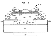
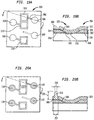
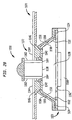
- FIG. 1 is a sectional view of a packaged semiconductor chip 10.
- the packaged chip is shown in an orientation in which a front face 102 of the semiconductor chip faces downwardly.
- the packaged chip includes a semiconductor chip 100 having a front face 102 and a rear face 114 remote from the front face.
- the front face of the chip 100 is covered by a lid or cover 104 which is assembled together with the semiconductor chip 100 to form the packaged chip 10.
- the front face 102 of the semiconductor chip 100 is oriented downwardly towards an upwardly facing inner surface 105 of the lid 104.
- the semiconductor chip 100 typically includes a semiconductor substrate in which one or a plurality of semiconductor devices 112 are disposed in a device region thereof below the front face 102.
- the semiconductor chip 100 also includes a plurality of dielectric layers overlying the substrate, in which conductive metal wiring layers and vias (not shown) are disposed.
- the semiconductor devices 112 are disposed at the front face of the chip and/or between the front and rear faces of the chip.
- the semiconductor chip 100 typically is connected to the lid 104 through one or more standoff structures 124, which may include an adhesive, an inorganic or organic material and/or a joining metal. Structures for supporting a lid at a constant spacing from a chip are described in the commonly owned U.S. Provisional Application No. 60/761,171 filed on January 23, 2006 , and U.S. Provisional Application No. 60/775,086 filed on February 21, 2006 .
- the packaged chip may include an interior cavity 106 between the front face 102 of the chip and the inner surface 105 of the lid 104, as illustrated in FIG. 1 .
- the packaged chip 10 can be constructed without an interior cavity.
- the cavity's height 108 and the lateral dimensions, including lateral dimension 110 are typically determined, as for example, by the height and dimensions of the structure 124 used to assemble the lid 104 with the semiconductor chip 100.
- the lid 104 consists essentially of a glass or polymeric material and is at least partially transparent to electromagnetic spectra at frequencies of interest.
- the lid 104 may be only partially transparent to provide a filter function, or may be essentially transparent to a range of frequencies of interest.
- the semiconductor devices 112 in the semiconductor chip 100 typically include electromagnetic transducer devices such as electromagnetic or electro-optic devices which either detect or output electromagnetic radiation.
- the semiconductor devices may be designed to emit or receive radio frequency and/or optical wavelengths of infrared, visible and/or ultraviolet or higher wavelength spectra including but not limited to x-ray wavelengths.
- the semiconductor devices 112 can include acoustic transducer devices, such devices being designed to convert sound pressure waves received through a medium, e.g., air and/or other fluid medium (gas or liquid) to one or more electrical signals, or to convert one or more electrical signals into sound pressure waves.
- the packaged chip is a sensor unit in which the semiconductor devices 112 of the chip 100 include an imaging area 107 for capturing an image.
- Electronic circuits (not shown) in chip 100 are connected to the semiconductor devices in the imaging area 107 for generating one or more electrical signals representing an image captured by the imaging area 107.
- Numerous electrical circuits are well known in the imaging art for this purpose.
- the semiconductor chip 100 may be a generally conventional charge-coupled device (CCD) imaging chip with conventional circuits such as clocking and charge-to-voltage conversion circuits.
- CCD charge-coupled device
- the semiconductor chip includes a plurality of front contact pads 116 overlying an insulative or "passivation" layer 118 at the front face of the semiconductor chip.
- the passivation layer preferably includes an inorganic dielectric or organic dielectric material.
- the passivation layer 118 preferably includes a dielectric material such as silicon dioxide, silicon nitride and/or a combination of materials such as a layered stack including silicon dioxide and silicon nitride.
- the semiconductor devices 112 in the device region are conductively connected to the front contact pads 116. The semiconductor device, thus, are accessible conductively through wiring incorporated within one or more layers of the semiconductor chip 100 below and/or within the passivation layer 118.
- a second insulative layer 122 is disposed along edges 120 of the semiconductor chip 100.
- the insulative layer 122 preferably includes a conformally coated dielectric material.
- the conformal coating covers at least portions of the edges 120 and rear surface 114 of the chip.
- the conformal coating covers the edges and rear face of the semiconductor chip continuously and uniformly, such that there are no breaks in the conformal coating and the insulative layer 122 provides good dielectric isolation with respect to the semiconductor chip 100.
- a plurality of conductive traces 126 conductively connect the front contact pads 116 of the chip to corresponding package contact pads 128 which overlie an exterior surface of the packaged chip 10.
- the package contact pads 128 overlie the rear surface 114 of the semiconductor chip 100.
- the conductive traces 126 overlie the second insulative layer 122 and extend over portions of the edges 120 and rear surface 114 of the semiconductor chip.
- the conductive traces 126 preferably connect individual front contact pads 116 of the chip 100 with corresponding individual package contact pads 128 and conductive bumps 134.
- a third insulative layer 130 overlies the conductive traces 126 and provides external isolation therefor.
- This layer can be referred to as an "external passivation layer" 130 of the package 10.
- a metal structure 132 including a metal layer or stack of metal layers including a wettable metal layer overlies the package contact pads 128, and conductive bumps 134 overlie the metal structure 132.
- the conductive bumps 134 include a fusible metal having a relatively low melting temperature such as solder, tin, or a eutectic mixture including a plurality of metals.
- the bumps 134 include a wettable metal, e.g., copper or other noble metal or non-noble metal having a melting temperature higher than that of solder or other fusible metal. Such wettable metal can be joined with a corresponding feature, e.g., a fusible metal feature of an interconnect element such as a circuit panel to externally interconnect the packaged chip 10 to such interconnect element.
- the bumps 134 include a conductive material interspersed in a medium, e.g., a conductive or solder-filled paste and/or an isotropic or anisotropic conductive adhesive.
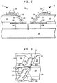
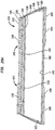
- FIG. 2 is a partial sectional view through portions of two packaged chips 10.
- the packaged chips 10 include semiconductor chips 100 which remain connected by a standoff structure 206 and a lid element or lid wafer 204 having dimensions corresponding to the semiconductor element or wafer including chips 100.
- the packaged chips 10 are severed from each other along a dicing lane 208 of the lid element 204 to form individual packaged chips 10, each packaged chip 10 being as illustrated in FIG. 1 .
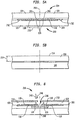
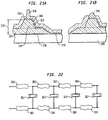
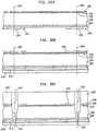
- FIG. 3 A method of simultaneously fabricating a plurality of packaged chips 10 ( FIG. 1 ) will now be described, with reference to FIGS. 3 through 14 .
- portions of semiconductor material of a plurality of semiconductor chips 100 which are registered with the front contact pads 116 of the semiconductor chips are removed from a rear face 114 thereof.
- One or more junction portions 300 of semiconductor material disposed between edges 120 of the semiconductor chips 100 are purposely allowed to remain after this process.
- the presence of the one or more junction portions 300 provides conductive continuity between exposed external edges of the semiconductor chips 100 during the formation of an dielectric isolation coating 122 ( FIG. 1 ) overlying the edges 120 and rear faces 114 of the semiconductor chips.
- the dielectric coating 122 is formed by electrodeposition, preferably by electrophoretic deposition of a polymer.
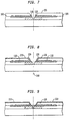
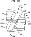
- FIG. 4A illustrates a preliminary stage of fabrication in which a plurality of standoff structures 206 are formed extending outward from a major surface of a lid element 204.
- Each standoff structure 206 typically has a rectangular shape aligned with dicing lanes 208 which lie at the boundaries between individual lids to be severed from the original lid element 204.
- dicing lanes 208 which lie at the boundaries between individual lids to be severed from the original lid element 204.
- the standoff structure 206 has a form which can be described as that of a "picture frame ring shape.”
- the standoff structure can include one or more inorganic and/or organic dielectric materials, semiconductors and/or conductors such as one or more metals.
- the standoff structure can be fabricated by additive and/or subtractive processing, as described in, for example, U.S. Patent Application No. 10/949,674 filed September 24, 2004 , or U.S. Provisional Application No. 60/761,171 .
- the standoff structure When the standoff structure includes a metal, it can be fabricated by a combination of steps including sputtering of a thin layer of metal followed by subtractive patterning and then electroplating the remaining structure with a final metal. Alternatively, the standoff structure can be formed by electroless plating, followed by subtractive patterning and electroplating.
- the standoff structure 206 is fabricated by electrophoretic deposition of a polymer onto a preexisting sputtered or plated conductive layer, in a manner such as that described in U.S. Provisional Application No. 60/775,086 .
- FIG. 5A illustrates a subsequent stage of fabrication after a semiconductor element 200 (a portion of or an entire semiconductor device wafer) has been joined to a corresponding lid element.
- a passivation layer 118 and then front contact pads 116 are formed, the front contact pads 116 being exposed at the front surface of each semiconductor chip 100.
- the front contact pads 116 may be of a type commonly referred to as "compatible pads.”
- Compatible pads are typically formed in such way as to conductively connect to other contacts, e.g., pads 212 of each chip 100 which are farther away (in a lateral direction 210) from the dicing lanes, e.g., dicing lane 208.
- the front contact pads 116 e.g., the compatible pads, are not conductively connected to other corresponding front contact pads across the intervening dicing lane 208. However, they can be so connected.
- portions of two semiconductor chips 100 of a larger semiconductor element 200 are shown as attached through supporting structures 206 to corresponding portions of a lid element 204 which includes lids 104.
- semiconductor chips 100 are joined together at boundaries such as the boundary defined by dicing lane 208.
- the semiconductor element 200 is shown inverted in relation to the view shown in FIG. 5A .
- a thickness of the semiconductor element 200 has been reduced, as by grinding and/or lapping from a rear face 114 thereof. Reducing the thickness of the semiconductor element 200 can assist in achieving a final packaged chip having a desirably small thickness 214.
- the lid element 104 overlying the front face of the semiconductor chip assists in providing structural support to the semiconductor chip, increasing its rigidity to permit the thickness of the packaged chip to be reduced as desirable to a smaller thickness.
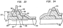
- FIG. 6 a subsequent stage of fabrication is shown in FIG. 6 in which an opening 216 is formed the semiconductor element 200 in registration with the dicing lane 208 between adjacent semiconductor chips 100. Openings preferably are formed which extend along the length of each edge 120 of each semiconductor chip as viewed in FIG. 3 . Openings like the opening 216 shown in FIG. 6 preferably are formed by depositing a photoimageable layer 218, e.g., a photoresist, antireflective coating or other layer, patterning openings in the photoimageable layer by photolithography and then etching the semiconductor element from the rear face 114 in accordance the openings therein.
- a photoimageable layer 218, e.g., a photoresist, antireflective coating or other layer e.g., a photoresist, antireflective coating or other layer
- each chip 100 which are exposed at the walls of the openings preferably are oriented preferably at an angle 248 of between about 10 and 60 degrees from a normal 246 to the front face of the semiconductor chip.
- the semiconductor element is etched isotropically using an etchant which attacks the semiconductor material, e.g. silicon, of the semiconductor element but which does not attack a material included in the passivation layer 118.
- the passivation layer functions as an etch stop protecting the front contact pads 116 when openings in the semiconductor element 200 are etched.
- the patterned photoimageable layer is removed from the assembly.
- the assembly appears as shown in FIG. 3 , having semiconductor material portions removed where they overlie the front contact pads 116.
- the passivation layer overlying the contact pads 116 is not shown in FIG. 3 .
- the assembly including the semiconductor element with the lid element attached thereto is then immersed in a dielectric deposition bath. The assembly is then held there under appropriate conditions for a sufficient time to form an electrodeposited conformal dielectric coating 220 on exposed exterior conductive and/or semiconductive surfaces of the semiconductor element.
- an electrophoretic deposition technique is utilized to form the conformal dielectric coating, such that the conformal dielectric coating is only deposited onto the exposed conductive and/or semiconductive surfaces of the assembly.
- the electrophoretically deposited coating is self-limiting in that after it reaches a certain thickness governed by parameters, e.g., voltage, concentration, etc. of its deposition, deposition stops.
- Electrophoretic deposition forms a continuous and uniformly thick conformal coating where on conductive and/or semiconductive exterior surfaces of the assembly.
- the electrophoretically deposited coating preferably does not form on the passivation layer 118, due to its dielectric (nonconductive) property.
- the conformal coating is formed from a cathodic epoxy deposition precursor.
- a polyurethane or acrylic deposition precursor could be used.
- electrophoretic coating precursor compositions and sources of supply are listed in Table 1 below.
- Table 1 ECOAT NAME POWERCRON 645 POWERCRON 648 CATHOGUARD 325 MANUFACTURERS MFG PPG PPG BASF TYPE CATHODIC CATHODIC CATHODIC POLYMER BASE EPOXY EPOXY EPOXY LOCATION Pittsburgh, PA Pittsburgh, PA Southfield, MI APPLICATION DATA Pb/Pf-free Pb-free Pb or Pf-free Pb-free HAPs, g/L 60-84 COMPLIANT VOC, g/L (MINUS WATER) 60-84 ⁇ 95 CURE 20 min/175C 20 min/175C FILM PROPERTIES COLOR Black Black Black Black THICKNESS, ⁇ m 10-35 10-38 13-36 PENCIL HARDN
- processing is then begun for forming conductive traces which connect the front contact pads of the semiconductor chips to exterior contacts of the packaged chips.
- portions of the dielectric passivation layer 118 extending beyond the conformal dielectric coating 220 at edges 120 of the semiconductor chips is now removed. Removal of the passivation layer can be performed, for example, through use of an etchant which attacks the passivation layer 118 while not substantially attacking the conductive material, e.g., one or more metals which are included in the front contact pads.
- An exemplary process for etching the passivation layer includes plasma etching performed in a manner which selectively does not attack organic materials so as to preserve the exposed conformal dielectric coating 220.
- a groove is cut between the standoff structures on each side of the dicing lane, such as through use of a saw designed to make a "V"-shaped groove several microns in width. This process exposes conductive edges of the front contact pads along walls of the V-shaped groove.
- a metal layer 222 for forming conductive traces is deposited to overlie the conformal dielectric coating 220.
- the metal layer preferably is deposited by sputtering a primary metal layer onto exposed surfaces of the assembly, or by electroless deposition.
- the primary metal layer includes or consists essentially of aluminum.
- the primary metal layer includes or consists essentially of copper.
- the primary metal layer includes or consists essentially of titanium.
- One or more other exemplary metals can be used in a process to form the primary metal layer.
- a photoimageable layer is deposited to overlie the primary metal layer and a three-dimensional photolithographic patterning process is utilized to pattern the primary metal layer, such as the process described in U.S. Patent No. 5,716,759 to Badehi .
- the photoimageable layer is removed from the semiconductor element and an electroplating process is used to plate a secondary metal layer onto the primary metal layer to form individual conductive traces 226 extending from the front contact pads 116 along edges 120 and onto the rear faces 114 of the semiconductor chips.
- the secondary metal may include nickel or other noble metal.
- the electroplated second metal on the primary metal layer completes the conductive traces.
- an optional third metal layer such as gold, platinum or palladium may be plated onto the secondary metal for providing corrosion resistance to complete the conductive traces.
- a plug 224 including the second metal layer and optional third metal layer forms overlying exposed surfaces of the front contact pads 116 and which may line or fill the gap between adjacent standoff structures 206.
- FIGS. 11-14 further processing is performed to define package contacts overlying the rear face 114 of the semiconductor chips.
- an additional photoimageable layer 230 is deposited and patterned to cover portions of the conductive traces 226 where wettable metal contacts and preferably conductive bumps are to be formed.
- a further process is performed to passivate exterior surfaces of the packaged chips.
- a further electrophoretic process is employed to form a third insulative layer including uniformly thick conformal dielectric coating 232 overlying each of the conductive traces 226 on the rear surface 114 and edges 120.
- the metal plugs 224 provide conductive continuity between semiconductor chips 100 of the semiconductor element.
- the photoimageable layer 230 is removed by selective removal process, such as dissolution in a solvent or selective etching.
- FIG. 12 illustrates a particular stage in processing after the external conformal dielectric coating 232 has been formed and the patterned photoimageable layer has been subsequently removed, leaving openings 228 in the external passivating layer 232.
- the conformal dielectric coating 232 can be formed by spin-coating and/or spray coating a photoimageable dielectric such as an encapsulant towards the rear face and edges 120 of the semiconductor chip to form a relatively uniformly thick coating. Thereafter, openings 228 are formed in the conformal dielectric coating 232 by photolithographic process. One or more processes, e.g., heating etc. may be performed to cause the conformal dielectric coating 232 to harden after the initial deposition of the photoimageable material.
- a photoimageable dielectric such as an encapsulant towards the rear face and edges 120 of the semiconductor chip
- conductive structures 236 including a wettable metal layer are formed within the openings of the passivating layer 232.
- wettable metal features 236 of the type commonly referred to as "under bump metallization" (“UBM”) are formed within the openings to overlie the conductive traces 226.
- the conductive bumps can include one or more conductive materials.
- the conductive bumps can include a fusible metal such as solder, tin, or a eutectic composition and/or one or more noble metals, for example, copper, nickel, etc.
- the conductive bumps are formed by placing spheres including a fusible metal such as solder, tin or eutectic onto the wettable metal features 236 and then heating the conductive bumps thereto to fuse them to the wettable metal features 236.
- the packaged chips are severed from each other along dicing lane 208 by sawing or other dicing method to form individual packaged chips as illustrated in FIG. 14 .
- a variety of exemplary processes for severing packaged chips into individual units are described in the commonly owned U.S. Provisional Application Nos. 60/761,171 and 60/775,086 , any of which can be used to sever the packaged chips to form individual packaged chips as shown in FIG. 14 .
- metal features 224 disposed between the front contact pads preferably are removed, such that individual ones of the front contact pads 116 on the semiconductor chips are conductively disconnected from each other.
- conductive features 310 at a front face 302 of a semiconductor chip 300 are covered with a dielectric material 304 by an electrophoretic deposition process.
- the electrophoretically deposited dielectric coating 304 serves as a dielectric level on which conductive traces 306 and additional conductive contacts 308 can be disposed above the front face 302 of the chip.
- the conductive traces 306 and additional conductive contacts 308 serve to redistribute the conductive contacts from the original contacts 310 of the chip.
- the conductive trace 306 has an advantageous microstrip line relationship with the conductive feature 316 on which the electrophoretic coating 304 is formed.
- a uniformly thick dielectric layer separates a signal-carrying conductor from another conductor, e.g., ground plane which is held at a reference potential such as ground or other typically fixed potential.
- the signal-carrying conductor includes trace 306 and contact pad 308, and the other conductor 316 at the front face 302 of the chip is held at fixed potential such as ground.
- Openings 325 in the electrophoretic coating 304 can be provided selectively, such that only certain contacts 310 of the chip are connected to conductive traces 306 and conductive pads 308 of the chip for redistribution. Other contacts of the chip can be connected to the ground plane or reference conductor 316 at the front face of the chip.
- FIGS. 15A and 15B illustrate a preliminary stage in the formation of the microelectronic structure 350.
- a plurality of exposed conductive contacts 310 are provided at the front face 302 of a microelectronic chip such as a semiconductor chip having active devices therein.
- a dielectric layer is provided in areas of the front face other than where the conductive contacts are exposed, such dielectric layer usually being referred to as a "passivation layer.”
- the conductive contacts 310 of the chip are shown arranged in a row. However, the contacts 310 need not be arranged in one line.
- the contacts 310 can be disposed at or near peripheral edges 314 of the chip or the contacts 310 can be disposed at locations farther away, or even well removed from the edges 314.
- the processing described herein for fabricating the structure shown in FIGS. 19A-19B is performed simultaneously to a plurality of chips while the chips remain attached together in form of a wafer or portion of a wafer.
- a masking layer 312 is formed in registration with at least some of the contacts 310 to prevent the electrophoretic coating from being formed thereon.
- an inorganic dielectric material such as an oxide of silicon having a thickness of 10 ⁇ m (microns) or greater is blanket-deposited to overlie the front face 302 of the chip.
- the layer of inorganic dielectric material is removed in areas except where the inorganic dielectric material overlies certain ones of the contacts 310.
- the inorganic dielectric layer remains as a masking layer over some, but not all of the contacts 310. For example, as shown in FIG. 16A , a particular contact 315 remains uncovered by the masking layer 312.
- a metal layer 316 is blanket deposited to overlie the front face 302 of the chip. Thereafter, the masking layer 312 ( FIGS. 16A-16B ) is removed from the contacts 310, leaving the previously masked contacts exposed once again. However, the blanket deposited metal layer is formed in conductive communication with the particular contact 315 that was not masked by masking layer 312. As will be described below, the blanket metal layer 316 is typically used for the purpose of a ground plane. Therefore, the particular contact 315 will be conductively connected to the blanket deposited metal layer when other contacts 310 are exposed after removal of the masking layer 312.
- the dielectric coating 304 has a thickness of between about one ⁇ m (micron) and 100 ⁇ m, and preferably between about one ⁇ m and 15 ⁇ m.
- the dielectric layer 304 has a substantially flat top surface 320 and typically has a gradual, sloping transition 305 between the front face 302 of the chip 300 and the top surface 320. This transition 305 may follow a line of curvature from the substantially flat top surface 320 or may simply be canted at an angle such that the transition 305 is not too vertically oriented in relation to the front face 302 and the top surface 320.
- the electrophoretically deposited layer 304 preferably includes a low modulus of elasticity material, such as may be obtained by electrophoretic deposition of polymeric materials such as flexibilized epoxy, silicones, acrylics, etc.
- a flexible electrophoretic coating capable of buckling or wrinkling to accommodate relative movement, can be fabricated from high elastic modulus materials, normally considered as "rigid,” provided that these materials are present in thin layers. Relatively soft materials can be used in greater thicknesses and provide a highly flexible coating.
- Such soft materials provide a highly compliant interposer or underlayer for the placement of conductive contacts thereon, i.e., an interposer which is readily compressible in the directions perpendicular its surfaces and which, therefore, permits movement of the terminals in these directions.
- An advantage of forming the dielectric coating by electrophoretic deposition is that deposition occurs in response to application of an electric field. Accordingly, conditions are most favorable for deposition in areas where a conductor is exposed and is held at a certain potential in relation to the fluid deposition medium. In other areas where no exposed conductor is present and where the electric field is much weaker, deposition is minimal or non-existent. For this reason, the electrophoretic coating does not form on conductors which are not conductively connected to the required source of electric potential, even when such conductors are exposed directly to the deposition medium. In this way, contact pads 310 which are not conductively connected to the metal layer 316 remain free or substantially free of the deposited coating after the electrophoretic deposition process.
- the thickness of the resulting dielectric layer varies in relation to the strength of the electric field. For this reason, as illustrated in FIGS. 18A and 18B , the thickness 322 of the electrophoretically deposited dielectric layer 304 generally is constant over interior portions 320 of a conductive planar surface such as the ground plane 316. On the other hand, the thickness of the electrophoretically deposited dielectric layer 304 decreases gradually from its nominal thickness 322 to zero at boundaries of the conductive surface, i.e., at edges of the conductive surface. The resulting dielectric layer has a sloped edge, rather than an abrupt edge.
- the electrophoretic dielectric coating 304 extends somewhat beyond the edges 324 of the conductive surface. In this way, the dielectric coating 304 overlies portions 326 of the front face 302 of the chip adjacent to edges 324, but tapers off to zero thickness to leave contacts 310 exposed.
- conductive traces 306 are formed which extend along the top surface of the dielectric and down the sloped edges to conductively connect to the original conductive contacts 310 of the chip 300.
- the sloping edges of the dielectric layer 334 enable conductive traces 306 to be provided which are subject to substantially less fatigue from thermal and mechanical stresses than would be the case if the edges of the dielectric layer 304 were at right angles to its top and bottom surfaces.
- outer conductive contacts 308, e.g., lands, are formed together with the conductive traces 306 in locations overlying an exposed surface of the dielectric coating 304.
- the fabrication of these additional lands 308 and traces 306 can be performed by processing as described above with reference to FIGS. 9 through 12 . Further processing similar to that described with reference to FIGS. 13-14 above can be performed to fabricate ball grid array ("BGA") contacts and to sever individual chips from a larger assembly, e.g., semiconductor wafer or portion of semiconductor wafer.
- BGA ball grid array
- a solder mask or other type of external passivation layer 321 can be formed, electrically isolating the original chip contacts 310, while leaving the contacts 308 exposed as lands or bond pads for the interconnection of bond wires thereto.
- FIGS. 20A-20B illustrate a variation of the embodiment shown and described with reference to FIGS. 19A-19B above.
- a plurality of post-like or pin-like contacts 318 project upwardly from contact pads 308 overlying the electrophoretically deposited dielectric layer.
- the contacts 318 are solid metal features and have frustum, conical or pyramidal shape.
- the contacts 318 extend to a height 335 of about 100 ⁇ m above the surface of the contact pad 308, have a diameter at a base surface of about 200 ⁇ m, and have a diameter at a top surface or "tip" of about 50 ⁇ m.
- the contacts consist essentially of a metal such as copper or other metal which has a melting temperature higher than that of a fusible metal, e.g., solder.
- a fusible metal e.g., solder.
- contacts 318 remain solid during processes used to bond the contacts 318 of the chip to other microelectronic structures as a chip carrier, interposer, circuit panel or the like.
- the contacts 318 can be fabricated through an additive process such as electroplating, or via transfer from an adhesively backed article and metallurgical bonding the contacts 318 to the contact pads.
- the contacts 318 can be fabricated via subtractive processing such as etching from a metal layer in accordance with a mask pattern.
- an additional dielectric layer 321 overlies the surface of the conductive traces 306 and contact pads 308 as an external passivation layer or solder mask.
- the thickness of the electrophoretically deposited dielectric layer 304 is constrained by the thermal-mechanical properties of the semiconductor wafer, e.g., silicon wafer and those of the dielectric layer. Even when the modulus of the dielectric layer 304 is quite low, the product of the thickness, the modulus and the mismatch between the thermal expansion coefficients of the two materials can cause the wafer to warp or bow under a relatively large change in temperature when the thickness of the dielectric layer is sufficient. Any warping of the semiconductor wafer is problematic because equipment and facilities are designed to process semiconductor wafers which are planar or have nearly perfect planarity.
- FIG. 21A illustrates a further variation of the above-described embodiment in which the thickness of the dielectric layer is made greater in locations where the dielectric is disposed between the conductive plane and individual external contact pads 308. Increasing the thickness of the dielectric layer in such locations allows the external contact pads 308 to be placed at greater height above front surface while keeping stresses due to thermal expansion mismatch at a manageable magnitude.
- the dielectric layer includes an initial dielectric layer 304 which is electrophoretically deposited as described above. After forming that layer 304, a region 334 of additional compatible dielectric material is formed in specific locations overlying the dielectric layer 304. In such way, dielectric region 334 and dielectric layer 304 together form a combined region of dielectric material between the contact pad 308 and the conductive plane 316, the combined region having a thickness 330 from the conductive plane 316 which is greater than that of the original dielectric layer.
- the additional region 334 includes a different material than that of the electrophoretically deposited dielectric layer 304.
- the additional region 334 has a lower modulus than that of the electrophoretic dielectric layer 304.
- the increased thickness of the combination of the additional region with the electrophoretic dielectric layer 304 provide a higher degree of compliancy than either layer provides by itself.
- one or both of the dielectric layer 304 and the additional region 334 are relatively compliant, i.e., have relatively low modulus and sufficient thickness.
- the compliant material below the base of the contact 318 can flex. This permits the tip of the contact 318 to remain in mating contact with the terminal of the external element even when the mating surfaces of contacts and the external terminals are not perfectly planar.
- FIG. 21B is a sectional view illustrating a microelectronic structure in accordance with a variation of the embodiment depicted in FIG. 21A .
- the contact includes a bump 340 including a fusible metal such as solder, tin or eutectic composition, instead of a post-like protrusion 318 ( FIG. 21A ).
- the bump 340 can include a solid or hollow core and a coating of such fusible material, the core containing one or more other materials such as copper or a polymer.
- the bump 340 is arranged as one of many bumps overlying similar raised regions 334 of dielectric material in an arrangement referred to as a "ball grid array" (BGA).
- BGA ball grid array
- FIG. 22 is a diagram of a network which models the electrical impedance characteristics of the structure illustrated in FIG. 21A .
- inductance and capacitance in the network is distributed, as modeled by inductors 360 and capacitors 362, which occur as parallel-disposed impedance elements in the network.
- capacitance and inductance are constant throughout the network.
- each of the conductive traces 346 shown in FIGS. 21A-B varies with position along their lengths.
- the values of these parameters depend on the type of dielectric material in the dielectric regions 334, 304, as well as the thickness of the dielectric material from conductive plane 316 and the width of the conductive traces.
- the dielectric characteristics of regions 304, 334 are constant with position along the length of each trace.
- the width of each trace is also constant. For a variety of reasons, it is impractical for the widths of the traces 346 to vary between the original contacts 310 of the chip and the outer contacts 308.
- the increased thickness of the dielectric material directly underlying the contacts 318 causes the inductance and capacitance seen by the traces to vary along their length. Variations in impedance of this sort are problematic. Decreased tuning of the circuit and losses due to signal reflection can result.
- the surface of the lower conductor 336 is arranged such that it remains parallel to the external conductive traces 346 at a constant or near constant spacing thereto.
- a flat portion 356 of the lower conductor extends a distance along the front face of the chip.
- the lower conductor jogs upward along a wall portion 337 adjacent to a dielectric region 344.
- the wall portion 337 preferably is sloped such that the flat portion 356 is not at a right angle with the wall portion 337. Rather, the flat portion makes a gradual transition with the wall portion.
- An upper flat portion 366 also makes a gradual transition with the wall portion 337 at a location overlying dielectric region 344.
- Fabrication of the microelectronic structure illustrated in FIG. 23 is similar to that of the structure shown in FIG. 21A . However, in this case, an additional dielectric region 344 is formed prior to forming the lower conductor and then forming the electrophoretically deposited dielectric coating 368 overlying the lower conductor 336.
- the substantially uniform thickness 362 of the dielectric coating 368 results from the electrophoretic deposition technique used to form the dielectric coating thereon.
- electrophoretic deposition has a self-limiting quality such that its thickness is related to the strength of the electric field. Therefore, the electrophoretically deposited coating takes on the profile of the conductor which underlies the coating. For this reason, the conductive traces 346 of the resulting structure, shown in FIG. 23 , remain at constant spacing to the lower conductor 336, to provide a transmission line having constant impedance.
- FIG. 24 illustrates a variation of the structure illustrated in FIG. 23 , in which a conductive bump 370, rather than a post-like contact, is provided for externally connecting the chip to terminals of an external microelectronic element.
- a camera module 1030 includes a sensor unit 1020 having contacts 1042 disposed on the rear face of the sensor unit, i.e., on the surface of the semiconductor chip 1000 opposite from the front surface 1028 which carries the imaging area 1026.
- the sensor unit can be such as that shown and described above with reference to FIG. 1 .
- Similar sensor units and camera modules are described in commonly owned United States Patent Application Nos. 11/265,727 filed November 2, 2005 and 11/322,617 filed December 30, 2005 , further identified as attorney docket numbers TESSERA 3.0-381 CIP and 3.0-464.
- the contacts 1042 of the sensor unit are connected to terminals 1080 of a circuit panel 1070 by masses 1082 of fusible conductive material such as solder.
- the optical unit 1050 in this arrangement includes a turret or support structure 1051 having a mounting portion 1052 arranged to hold one or more lenses or other optical elements 1058.
- the support structure 1051 also includes a plurality of rear elements 1062 in the form of elongated posts 1062 projecting rearward from the mounting portion 1052. These posts have rear surfaces 1054 which abut or mechanically engage a reference plane in the sensor unit to position the optical unit relative to the sensor unit. In the example illustrated in FIG. 25 , the rear surfaces 1054 abut the front surface of the transparent cover 1034 which overlies the imaging area 1026.
- the turret or support structure includes registration features, e.g., posts, pins, recesses, or the like, for mechanically setting the height of the optical unit 1050 with respect to the chip 1000, while limiting tilt of the turret with respect to the imaging area 1026 of the chip.
- connection between the rear surfaces of the posts 1062 and the front surface 1034 level and uniform in thickness.
- metallic attachment features or pads 1055 can be provided at the outer surface 1036 of the cover 1034, which are metallurgically bonded, e.g., via diffusion bonding, to metallic features at the rear surfaces 1054 of the posts 1062.
- a somewhat thin adhesive can be used to bond the rear surfaces of the posts to the cover.
- the turret or support structure 1051 in place of posts, includes a rear element which encloses or substantially encloses a volume having a cylindrical or polyhedral shape.
- a rear element can be provided which has a cylindrical wall or polyhedral shaped (e.g., box-shaped) wall, in which the rear surface of the rear element abuts against a reference plane of the sensor unit such as provided at the outer surface 1036 of the cover 1034.
- sensor unit 1020 is mounted with the front of the sensor unit, and hence, imaging area 1028 facing forwardly, toward the rear or bottom surface of circuit panel 1070.
- the contacts 1042 of the sensor unit are connected by suitable leads or wire bonds 1002 to the conductors 1076 of the circuit panel.
- the rear elements 1062 of the optical unit 1050 project through a hole 1072 in the circuit panel aligned with the imaging area 1028. Stated another way, hole 1072 is large enough to accommodate the light path from the optical element to the imaging area and also accommodate the rear elements 1062.
- a similar arrangement can be used with sensor units having contacts on the front face, as discussed above.
- a camera module in accordance with a further embodiment includes a sensor unit 920, depicted in broken lines, disposed on the bottom or rear side of a circuit panel 970.
- the optical unit 950 in this arrangement includes a turret or support structure 952 having a mounting portion 902 arranged to hold one or more lenses or other optical elements 958.
- the support structure 952 also includes a plurality of rear elements 962 in the form of elongated posts projecting rearward from the mounting portion 902. These posts extend through apertures 974 in the circuit panel, and thus mechanically engage the sensor unit to position the optical unit relative to the sensor unit as discussed above.
- posts define gaps between them as, for example, gap 963a between posts 962a and 962b.
- the circuit panel 970 may extend into the gaps, and hence may extend between the sensor unit and optical unit, which facilitates making connections to the sensor unit as discussed above.
- the gaps have substantial height.
- the height H G of the gap in the completed assembly is equal to the height of the mounting element 902 above the front surface 901 of circuit panel 970.
- the height H G desirably is on the order of 2 mm or more, more desirably 5 mm or more, and most preferably 1 cm or more.
- each gap i.e., the horizontal distance, parallel to the circuit panel, between rear elements 962a and 962b
- the width of each gap desirably also is at least about 2 mm, more desirably at least about 5 mm, and most desirably at least about 1 cm.
- provision of such large gaps allows access into the area between the optical element and hole 972 for performing operations on the completed assembly.
- the large gaps can be provided without increasing the overall height of the assembly.
- the distance between the optical elements such as lens 958 and the sensor unit is set by the optical properties of the system as, for example, the focal length of lens 958. Therefore, the lens must be supported at a substantial distance forward of the circuit panel in any event.
- a module or assembly in accordance with the embodiment of FIG. 27 can be treated after assembly by performing operations on the sensor unit through the gap or gaps, and desirably also through hole 972 in the circuit panel.
- the assembly may be subjected to a cleaning operation in which a cleaning fluid, a cleaning implement, or both are inserted into one or more of the gaps and through hole 972 to clean the surface of the sensor module.
- the sensor module incorporates a cover facing forwardly toward the rear or bottom surface of the circuit panel
- the area of the cover aligned with the hole which includes the area aligned with the imaging area of the sensor chip can be cleaned. The ability to perform such a cleaning operation on the completed assembly counteracts the effects of contamination during the assembly process.
- the sensor unit may not incorporate a separate cover, but instead may consist only of a "bare" semiconductor chip having an imaging area and having a passivation layer in the form of a thin coating effective to protect the elements of the bare chip from chemical or mechanical damage during the assembly process.
- a bare imaging chip typically requires very stringent precautions during handling to avoid deposition of dirt overlying one or more imaging elements. The requirements are somewhat less stringent for sensor units which incorporate a cover. However, by post-cleaning after assembly, the less stringent requirements may be applied to assembly of sensor units which do not include a cover.
- the sensor unit may include a sacrificial layer overlying the front of the sensor unit as, for example, a sacrificial layer overlying the outer surface of the cover in a sensor unit which includes a cover, or a sacrificial layer overlying the imaging area of the chip in a sensor unit which does not include a cover.
- the assembly is fabricated with the sacrificial layer in place.
- the completed assembly is then subjected to an operation in which the sacrificial layer, or at least that portion of the sacrificial layer aligned with the imaging area of the sensor unit, is removed through hole 972 and through the one or more of the gaps 963 in the support structure 952.
- the sacrificial layer may be removed by dissolving it, or by mechanically engaging it and peeling it away from the sensor unit. Removal of the sacrificial layer removes any contaminants which may have accumulated on that layer.
- a tool may be inserted into the gap or gaps to engage the conductors of the circuit panel and bond them to the contacts of the sensor unit.
- a wire-bonding tool may be used to provide wire bonds extending between the conductors and the sensor unit through hole 972, or through one or more of the additional apertures 974, or through other apertures (not shown) provided in the circuit panel for this purpose.
- the rear elements may be in the form of plates or ribs. Also, it is not essential to provide multiple gaps; only one gap may be sufficient for some operations.
- FIG. 28 illustrates an optical unit or camera module in accordance with another embodiment .
- a sensor unit 1120 has contacts 1142 conductively connected to terminals 1144 of a circuit panel which overlies the outer surface 1138 of the cover 1128, e.g., via solder masses 1146.
- Walls 1130 of the cover are preferably sloped such that the radii at edges 1132 of the walls are gradual and preferably provide a smooth transition between a set of first contacts 1134 provided on the front surface 1102 of the chip and the walls 1130.
- a dielectric coating 1158 such as an epoxy or other polymeric material deposited preferably via electrophoretic deposition, overlies the conductive traces 1156 and is utilized as a passivation layer, e.g., solder mask with openings exposed above the contacts 1142.
- an optical unit 1150 has a set of rear elements 1162 which extend rearward from a structure supporting an optical element 1158, e.g., a lens or other optical device selected from, among others, refractive or diffractive elements, filters, reflectors and scatterers.
- an optical element 1158 e.g., a lens or other optical device selected from, among others, refractive or diffractive elements, filters, reflectors and scatterers.
- rear surfaces 1164 of the rear element are adapted to extend through a hole 1172 in the circuit panel to abut or engage the outer surface 1138 of the cover 1128 or other reference plane of the sensor unit 1120.
- the circuit panel has a hole extending through the panel in alignment with the imaging area of the sensor unit. Such a hole forms a transparent region in the circuit panel.
- the circuit panel includes a solid but transparent region in alignment with the imaging area of the sensor unit.
- the circuit panel may be formed from a transparent dielectric material, in which case the transparent region of the circuit panel may be provided simply by routing the conductors of the circuit panel so that no conductors cross the transparent region.
- a packaged chip 1350 according to a further embodiment is shown in FIG. 29A which includes both top conductive contacts 1308 and bottom contacts 1404. Since the outer dimensions of the packaged chip 1350 are about the same as the dimensions of the original chip 1300, the packaged chip can be referred to as a "chip-scale" packaged chip. The packaged chip can be advantageously incorporated into a stacked microelectronic assembly as described with reference to FIG. 31 below.
- a semiconductor chip includes conductive features including a conductive layer, e.g., ground plane 1316, and original contacts 1310 at a front face 1302.
- the conductive layer 1316 if not already present at the front face 1302, can be formed by sputtering, plating or a combination therof, for example, as a prelude to subsequent processing, e.g., electrophoretic deposition of dielectric layer 1304.
- the electrophoretically deposited dielectric coating 1304 serves as a dielectric level on which a first metal layer 1306 is disposed above the front face 1302 of the chip.
- a second dielectric layer 1305 serves as a dielectric layer on which top traces 1312 and top contacts 1308 (connected through openings 1426 to the first metal layer are disposed.
- First metal layer 1306, top contacts 1308, top traces 1312, bottom contacts 1404 overlying the rear surface 1403 and edge conductive traces 1408 along edges, 1422 are in conductive communication with original contacts 1310 of the chip, the conductive traces 1306, top contacts 1308, top traces 1312, bottom contacts 1404 and side conductive traces 1408, serve to redistribute the conductive contacts from the original contacts 1310 of the chip.
- FIG. 29B is a front plan view looking towards the front surface 1302 showing top contacts 1308 and top traces 1312 overlying the front surface and side conductive traces 1408 along edges 1422 in conductive communication with the original contacts 1310 of the chip.
- FIG. 29C is a rear plan view showing bottom contacts 1404 and bottom traces 1405.
- dielectric layers 1305 and 1402 are deposited on to top and bottom surfaces 1403 of a microelectronic substrate such as a semiconductor wafer 1300. Boundaries between individual microelectronic elements, e.g., semiconductor chips of the wafer 1300 are indicated at 1500.
- the dielectric layers 1305, 1402 can be formed by an appropriate technique such as spin-coating, spray deposition, roller coating or vapor deposition, among others.
- the dielectric layer 1402 can be electrophoretically deposited onto the exposed semiconductor material at the bottom surface 1403 of the wafer by maintaining the wafer 1300 at an appropriate electric potential and immersing the wafer in an electrophoretic deposition bath as described above ( FIG. 7 ).
- bottom contacts 1404 are formed overlying the dielectric layer 1402.
- the bottom contacts 1404 are connected to bottom conductive traces 1405.
- the bottom contacts 1404 and bottom conductive traces 1405 can be formed, for example, by sputtering, plating and patterning techniques such as described above ( FIGS. 9-10 ).
- a carrier substrate or carrier wafer 1410 then is attached to the bottom of the wafer 1300 such as with a removable, e.g., peelable adhesive 1412 to form an assembly.
- openings 1420 aligned with the chip boundaries shown in FIG. 30B preferably can be formed by depositing a photoimageable layer 1430, e.g., a photoresist, antireflective coating or other layer, patterning openings in the photoimageable layer by photolithography and then etching the wafer 1300 from the rear face of the photoimageable layer.
- a photoimageable layer 1430 e.g., a photoresist, antireflective coating or other layer
- the openings 1420 may extend as channels across the length and width of the wafer
- the edges 1422 of each chip 1300 which are exposed at the walls of the openings preferably are oriented preferably at an angle of between about 10 and 60 degrees from a normal to the front face of the semiconductor chip.
- the semiconductor element is etched isotropically.
- the wafer 1300 can be sawn with a blade having a tapered profile to form the tapered openings 1420.
- FIG. 30D there is shown a partial perspective view facing a top surface illustrating the intermediate stage shown in FIG. 30C .
- the edges 1422 of each chip 1300 which are exposed at the walls of the openings are maintained in electrical continuity.
- the tapered openings 1420 are etched the channels separate the walls except for the corner area 1455, 1456 & 1457. While this exemplary embodiment shows the corner area with a mid section 1456 and sloped sections 1455 & 1457 other configurations are equally well suited. This corner area 1455, 1456 & 1457 maintains electrical continuity between the chips 1300.
- the patterned photoimageable layer is removed from the wafer.
- the assembly including the wafer and carrier wafer attached thereto is then immersed in a dielectric deposition bath.
- the assembly is then held there under appropriate conditions for a sufficient time to form an electrodeposited coating on exposed exterior conductive and semiconductive surfaces of the wafer 1300.
- an edge dialectric layer 1406 FIG. 30E
- a second top dielectric layer 1305 are formed such that the edge traces 1408 conductively communicate with the bottom traces 1405.
- the edge dielectric layer 1406 and second top dielectric layer 1305 can be formed by one or more of the above-described alternative methods, e.g., spin-coating, spray-coating, vapor deposition, etc.
- edge traces 1408 and top contacts 1308 are formed, such as by the sputtering, plating and patterning techniques described above ( FIGS 9-10 ). Openings 1426 formed in the top dielectric layer 1305, e.g., by laser drilling, patterned etching, or mechanical processes, allow the top contacts 1308 to connect to the first metal layer 1306.
- Lower circuit panel 1600 has a plurality of panel contact points 1610.
- Packaged chip 1350 is mounted on to the lower circuit panel 1600, whereby the panel contact points 1610 are in conductive contact with corresponding bottom contacts 1404 of the packaged chip 1350.
- the bottom contacts 1404 may be solder balls, previously described, as well as other contact types.
- Additional packaged chips 1350 may be stacked and mounted on top of the first packaged chip 1350.
- the bottom contacts 1404 of the additional packaged chip 1350 are in conductive contact with corresponding top conductive contacts 1308 of the initial packaged chip 1350.
- a top circuit panel 1650 has a plurality of lower panel contact points 1660.
- FIG. 31 shows a sandwich configuration with a plurality of packaged chips 1350 between a top circuit panel 1650 and a lower circuit panel 1600
- the present invention is equally well suited for other single circuit panel configurations.
- One or more packaged chips 1350 may be mounted on a lower circuit panel 1600 alone.
- One or more packaged chips 1350 may be mounted on a top circuit panel 1650 alone. Additional stacks of package chips 1350 as well as individual packaged chips 1350 may be mounted on the same circuit panel.
- one or more of the dielectric layers 1304, 1424 overlying the front surface 1302, the edges 1422, or the rear surface 1403 can be formed by techniques other than electrophoretic deposition, e.g., such as through use of spin-coating, spray deposition or vapor deposition among others.
- the first top dielectric layer 1304 is formed by techniques other than electrophoretic deposition. In such case, conductive layer 1316 at the front face 1302 can be omitted.
Claims (14)
- Procédé de fabrication d'une unité microélectronique, le procédé comprenant :la fourniture d'une tranche (1300) comportant une puce semi-conductrice présentant une surface avant (1302), une surface arrière (1403) distante de la surface avant, un matériau semi-conducteur exposé au niveau de la surface arrière, une couche conductrice (1316) exposée au niveau de la surface avant (1302), une pluralité de premiers contacts conducteurs (1310) exposée au niveau de la surface avant (1302), au moins certains des premiers contacts conducteurs (1310) étant isolés de la couche conductrice ;le dépôt par électrophorèse d'une couche isolante (1304, 1402) sur la couche conductrice exposée et le matériau semi-conducteur exposé ;la formation d'une pluralité de pistes conductrices arrière (1405) recouvrant la couche isolante (1402) au-dessus de la surface arrière (1403) de la puce semi-conductrice ;la formation d'une pluralité de pistes conductrices avant (1306) sur la couche isolante (1304) recouvrant la surface avant (1302) de la puce semi-conductrice en communication conductrice avec les premiers contacts conducteurs (1310) ;le dépôt par électrophorèse d'une autre couche isolante (1305) sur au moins une partie des pistes conductrices avant (1306) ;la formation d'une pluralité d'autres pistes conductrices (1312) sur au moins une partie de l'autre couche isolante (1305) recouvrant la surface avant (1302) de la puce semi-conductrice en communication conductrice avec les pistes conductrices avant ; etla formation d'une pluralité de pistes conductrices de bord (1408) qui s'étendent entre les pistes conductrices avant et arrière (1405), les pistes conductrices de bord (1408) étant formées par-dessus des surfaces de bord (1422) qui s'étendent entre la surface avant et la surface arrière de la puce semi-conductrice connectant ainsi de manière conductrice une ou plusieurs des pistes conductrices avant (1306) et des autres pistes conductrices (1312) aux pistes conductrices arrière (1405).
- Procédé selon la revendication 1, dans lequel la tranche comporte la puce semi-conductrice et au moins une autre puce semi-conductrice attachées ensemble à une ou plusieurs frontières périphériques (1500), les pistes conductrices arrière (1405) sont formées pendant que les puces restent attachées ensemble, et les surfaces de bord (1422) sont définies en éliminant du matériau d'une ou de plusieurs de la puce semi-conductrice et de l'au moins une autre puce semi-conductrice en alignement avec les une ou plusieurs frontières périphériques (1500).
- Procédé selon la revendication 1, dans lequel la couche isolante (1402) est déposée par électrophorèse sur le matériau semi-conducteur exposé au niveau de la surface arrière (1403) de la puce semi-conductrice simultanément au dépôt par électrophorèse de la couche isolante (1304) sur la couche conductrice exposée (1316).
- Procédé selon la revendication 1, dans lequel la couche isolante (1406) est déposée par électrophorèse sur le matériau semi-conducteur exposé au niveau des surfaces de bord (1422) avant la formation de la pluralité de pistes conductrices de bord (1408).
- Procédé selon la revendication 1, comprenant en outre la séparation de la puce semi-conductrice et de l'au moins une autre puce semi-conductrice le long d'une ou de plusieurs voies de découpe en alignement avec les une ou plusieurs frontières périphériques.
- Procédé de fabrication d'une pluralité d'unités micro-électroniques chacune selon la revendication 2, dans lequel les pistes conductrices arrière (1405) respectives de chacune de la pluralité de puces semi-conductrices sont formées pendant que la pluralité de puces semi-conductrices sont attachées ensemble, et les surfaces de bord (1422) de chacune de la pluralité de puces semi-conductrices sont définies en éliminant du matériau semi-conducteur en alignement avec une ou plusieurs frontières périphériques.
- Procédé selon la revendication 6, comprenant en outre la séparation de la pluralité de puces semi-conductrices le long d'une ou de plusieurs voies de découpe en alignement avec les frontières périphériques de chacune de la pluralité de puces semi-conductrices.
- Procédé selon la revendication 2, dans lequel la couche conductrice (1316) au niveau de la surface avant (1302) de chacune de la pluralité de puces semi-conductrices comporte un plan conducteur (1316) isolé des premiers contacts conducteurs (1310), le matériau isolant de cette puce semi-conductrice étant déposé par électrophorèse sur le plan conducteur.
- Procédé selon la revendication 2, dans lequel les surfaces de bord (1422) respectives de chacune de la pluralité de puces semi-conductrice sont inclinées à un angle aigu par rapport à la surface avant de cette puce semi-conductrice.
- Unité micro-électronique comprenant :une tranche (1300) une puce semi-conductrice présentant une surface avant (1302), une surface arrière (1403) distante de la surface avant, un matériau semi-conducteur exposé au niveau de la surface arrière, une couche conductrice (1316) exposée au niveau de la surface avant (1302), une pluralité de premiers contacts conducteurs (1310) exposée au niveau de la surface avant (1302), au moins certains des premiers contacts conducteurs (1310) étant isolés de la couche conductrice ;une couche isolante (1304, 1402) déposée par électrophorèse sur la couche conductrice exposée et le matériau semi-conducteur exposé ;une pluralité de pistes conductrices arrière (1405) recouvrant la couche isolante (1402) au-dessus de la surface arrière (1403) de la puce semi-conductrice ;une pluralité de pistes conductrices avant (1306) sur la couche isolante (1304) recouvrant la surface avant (1302) de la puce semi-conductrice en communication conductrice avec les premiers contacts conducteurs (1310) ;une autre couche isolante (1305) déposée par électrophorèse sur au moins une partie des pistes conductrices avant (1306) ;une pluralité d'autres pistes conductrices (1312) sur au moins une partie de l'autre couche isolante (1305) recouvrant la surface avant (1302) de la puce semi-conductrice en communication conductrice avec les pistes conductrices avant ; etune pluralité de pistes conductrices de bord (1408) qui s'étendent entre les pistes conductrices avant et arrière (1405), les pistes conductrices de bord (1408) étant formées par-dessus des surfaces de bord (1422) qui s'étendent entre la surface avant et la surface arrière de la puce semi-conductrice connectant ainsi de manière conductrice une ou plusieurs des pistes conductrices avant (1306) et des autres pistes conductrices (1312) aux pistes conductrices arrière (1405).
- Pluralité d'unités microélectroniques selon la revendication 10.
- Pluralité d'unités microélectroniques selon la revendication 11, dans lequel la couche conductrice (1316) au niveau de la surface avant (1302) de chacune de la pluralité de puces semi-conductrices comporte un plan conducteur (1316) isolé des premiers contacts conducteurs (1310), et sur lequel se trouve le matériau isolant déposé par électrophorèse.
- Pluralité d'unités microélectroniques selon la revendication 11, dans lequel les surfaces de bord (1422) respectives de chacune de la pluralité de puces semi-conductrices sont inclinées à un angle aigu par rapport à la surface avant de cette puce semi-conductrice.
- Unité microélectronique fabriquée par un procédé selon l'une quelconque des revendications 1 à 9.
Applications Claiming Priority (3)
| Application Number | Priority Date | Filing Date | Title |
|---|---|---|---|
| US11/590,616 US7935568B2 (en) | 2006-10-31 | 2006-10-31 | Wafer-level fabrication of lidded chips with electrodeposited dielectric coating |
| US11/789,694 US7807508B2 (en) | 2006-10-31 | 2007-04-25 | Wafer-level fabrication of lidded chips with electrodeposited dielectric coating |
| PCT/US2007/022518 WO2008054660A2 (fr) | 2006-10-31 | 2007-10-23 | Fabrication au niveau de la plaquette de puces à couvercle comportant une couche diélectrique appliquée par électrodéposition |
Publications (2)
| Publication Number | Publication Date |
|---|---|
| EP2087516A2 EP2087516A2 (fr) | 2009-08-12 |
| EP2087516B1 true EP2087516B1 (fr) | 2017-12-06 |
Family
ID=39344851
Family Applications (1)
| Application Number | Title | Priority Date | Filing Date |
|---|---|---|---|
| EP07852914.6A Active EP2087516B1 (fr) | 2006-10-31 | 2007-10-23 | Fabrication au niveau de la plaquette de puces à couvercle comportant une couche diélectrique appliquée par électrodéposition |
Country Status (4)
| Country | Link |
|---|---|
| US (1) | US7807508B2 (fr) |
| EP (1) | EP2087516B1 (fr) |
| KR (1) | KR20090093973A (fr) |
| WO (1) | WO2008054660A2 (fr) |
Families Citing this family (79)
| Publication number | Priority date | Publication date | Assignee | Title |
|---|---|---|---|---|
| US6211572B1 (en) * | 1995-10-31 | 2001-04-03 | Tessera, Inc. | Semiconductor chip package with fan-in leads |
| US8513789B2 (en) | 2006-10-10 | 2013-08-20 | Tessera, Inc. | Edge connect wafer level stacking with leads extending along edges |
| US7901989B2 (en) | 2006-10-10 | 2011-03-08 | Tessera, Inc. | Reconstituted wafer level stacking |
| US7829438B2 (en) | 2006-10-10 | 2010-11-09 | Tessera, Inc. | Edge connect wafer level stacking |
| US8569876B2 (en) | 2006-11-22 | 2013-10-29 | Tessera, Inc. | Packaged semiconductor chips with array |
| US7791199B2 (en) | 2006-11-22 | 2010-09-07 | Tessera, Inc. | Packaged semiconductor chips |
| US7952195B2 (en) | 2006-12-28 | 2011-05-31 | Tessera, Inc. | Stacked packages with bridging traces |
| JP5584474B2 (ja) | 2007-03-05 | 2014-09-03 | インヴェンサス・コーポレイション | 貫通ビアによって前面接点に接続された後面接点を有するチップ |
| US8461672B2 (en) | 2007-07-27 | 2013-06-11 | Tessera, Inc. | Reconstituted wafer stack packaging with after-applied pad extensions |
| CN103178032B (zh) | 2007-07-31 | 2017-06-20 | 英闻萨斯有限公司 | 使用穿透硅通道的半导体封装方法 |
| WO2009020572A2 (fr) | 2007-08-03 | 2009-02-12 | Tessera Technologies Hungary Kft. | Ensembles empilés utilisant des tranches reconstituées |
| US8043895B2 (en) | 2007-08-09 | 2011-10-25 | Tessera, Inc. | Method of fabricating stacked assembly including plurality of stacked microelectronic elements |
| TWI382477B (zh) * | 2007-08-24 | 2013-01-11 | Xintec Inc | 電子元件的晶圓級封裝及其製造方法 |
| US20100053407A1 (en) * | 2008-02-26 | 2010-03-04 | Tessera, Inc. | Wafer level compliant packages for rear-face illuminated solid state image sensors |
| US8680662B2 (en) | 2008-06-16 | 2014-03-25 | Tessera, Inc. | Wafer level edge stacking |
| KR20110051191A (ko) * | 2008-08-29 | 2011-05-17 | 버티칼 서킷, 인크. | 이미지 센서 |
| US20100055840A1 (en) * | 2008-08-29 | 2010-03-04 | Huang Chung-Er | Electronic packaging structure and a manufacturing method thereof |
| US20100207227A1 (en) * | 2009-02-16 | 2010-08-19 | Georg Meyer-Berg | Electronic Device and Method of Manufacturing Same |
| US8466542B2 (en) | 2009-03-13 | 2013-06-18 | Tessera, Inc. | Stacked microelectronic assemblies having vias extending through bond pads |
| US8796137B2 (en) * | 2010-06-24 | 2014-08-05 | Stats Chippac, Ltd. | Semiconductor device and method of forming RDL along sloped side surface of semiconductor die for z-direction interconnect |
| US8796135B2 (en) | 2010-07-23 | 2014-08-05 | Tessera, Inc. | Microelectronic elements with rear contacts connected with via first or via middle structures |
| US9640437B2 (en) | 2010-07-23 | 2017-05-02 | Tessera, Inc. | Methods of forming semiconductor elements using micro-abrasive particle stream |
| US8791575B2 (en) | 2010-07-23 | 2014-07-29 | Tessera, Inc. | Microelectronic elements having metallic pads overlying vias |
| US8847380B2 (en) | 2010-09-17 | 2014-09-30 | Tessera, Inc. | Staged via formation from both sides of chip |
| US8610259B2 (en) | 2010-09-17 | 2013-12-17 | Tessera, Inc. | Multi-function and shielded 3D interconnects |
| KR101059490B1 (ko) | 2010-11-15 | 2011-08-25 | 테세라 리써치 엘엘씨 | 임베드된 트레이스에 의해 구성된 전도성 패드 |
| US8308379B2 (en) | 2010-12-01 | 2012-11-13 | Digitaloptics Corporation | Three-pole tilt control system for camera module |
| US8637968B2 (en) | 2010-12-02 | 2014-01-28 | Tessera, Inc. | Stacked microelectronic assembly having interposer connecting active chips |
| US8736066B2 (en) | 2010-12-02 | 2014-05-27 | Tessera, Inc. | Stacked microelectronic assemby with TSVS formed in stages and carrier above chip |
| US8587126B2 (en) | 2010-12-02 | 2013-11-19 | Tessera, Inc. | Stacked microelectronic assembly with TSVs formed in stages with plural active chips |
| US8610264B2 (en) | 2010-12-08 | 2013-12-17 | Tessera, Inc. | Compliant interconnects in wafers |
| US8507316B2 (en) * | 2010-12-22 | 2013-08-13 | Taiwan Semiconductor Manufacturing Company, Ltd. | Protecting T-contacts of chip scale packages from moisture |
| US8552518B2 (en) | 2011-06-09 | 2013-10-08 | Optiz, Inc. | 3D integrated microelectronic assembly with stress reducing interconnects |
| US8546900B2 (en) | 2011-06-09 | 2013-10-01 | Optiz, Inc. | 3D integration microelectronic assembly for integrated circuit devices |
| US8546951B2 (en) | 2011-06-09 | 2013-10-01 | Optiz, Inc. | 3D integration microelectronic assembly for integrated circuit devices |
| US8604576B2 (en) * | 2011-07-19 | 2013-12-10 | Opitz, Inc. | Low stress cavity package for back side illuminated image sensor, and method of making same |
| US9018725B2 (en) | 2011-09-02 | 2015-04-28 | Optiz, Inc. | Stepped package for image sensor and method of making same |
| ITTO20110876A1 (it) * | 2011-09-30 | 2013-03-31 | Stmicroelectronics Malta Ltd | Metodo di saldatura di un cappuccio ad uno strato di supporto |
| US8796800B2 (en) | 2011-11-21 | 2014-08-05 | Optiz, Inc. | Interposer package for CMOS image sensor and method of making same |
| US8432011B1 (en) | 2011-12-06 | 2013-04-30 | Optiz, Inc. | Wire bond interposer package for CMOS image sensor and method of making same |
| US8570669B2 (en) | 2012-01-23 | 2013-10-29 | Optiz, Inc | Multi-layer polymer lens and method of making same |
| US8692344B2 (en) | 2012-03-16 | 2014-04-08 | Optiz, Inc | Back side illuminated image sensor architecture, and method of making same |
| US9233511B2 (en) | 2012-05-10 | 2016-01-12 | Optiz, Inc. | Method of making stamped multi-layer polymer lens |
| US9354486B2 (en) | 2012-06-07 | 2016-05-31 | DigitalOptics Corporation MEMS | MEMS fast focus camera module |
| US8921759B2 (en) | 2012-07-26 | 2014-12-30 | Optiz, Inc. | Integrated image sensor package with liquid crystal lens |
| US9007520B2 (en) | 2012-08-10 | 2015-04-14 | Nanchang O-Film Optoelectronics Technology Ltd | Camera module with EMI shield |
| US9001268B2 (en) | 2012-08-10 | 2015-04-07 | Nan Chang O-Film Optoelectronics Technology Ltd | Auto-focus camera module with flexible printed circuit extension |
| US9242602B2 (en) | 2012-08-27 | 2016-01-26 | Fotonation Limited | Rearview imaging systems for vehicle |
| US8759930B2 (en) | 2012-09-10 | 2014-06-24 | Optiz, Inc. | Low profile image sensor package |
| ITTO20120976A1 (it) * | 2012-11-09 | 2014-05-10 | St Microelectronics Srl | Procedimento per la fabbricazione di un cappuccio per una struttura di incapsulamento di dispositivi elettronici e cappuccio per una struttura di incapsulamento di dispositivi elettronici |
| US8988586B2 (en) | 2012-12-31 | 2015-03-24 | Digitaloptics Corporation | Auto-focus camera module with MEMS closed loop compensator |
| TWI549243B (zh) * | 2013-03-07 | 2016-09-11 | 精材科技股份有限公司 | 半導體結構及其製造方法 |
| US9190443B2 (en) | 2013-03-12 | 2015-11-17 | Optiz Inc. | Low profile image sensor |
| US9219091B2 (en) | 2013-03-12 | 2015-12-22 | Optiz, Inc. | Low profile sensor module and method of making same |
| US9142695B2 (en) | 2013-06-03 | 2015-09-22 | Optiz, Inc. | Sensor package with exposed sensor array and method of making same |
| US9496247B2 (en) | 2013-08-26 | 2016-11-15 | Optiz, Inc. | Integrated camera module and method of making same |
| US9461190B2 (en) | 2013-09-24 | 2016-10-04 | Optiz, Inc. | Low profile sensor package with cooling feature and method of making same |
| US9496297B2 (en) | 2013-12-05 | 2016-11-15 | Optiz, Inc. | Sensor package with cooling feature and method of making same |
| US9667900B2 (en) | 2013-12-09 | 2017-05-30 | Optiz, Inc. | Three dimensional system-on-chip image sensor package |
| US9494772B1 (en) | 2014-03-16 | 2016-11-15 | Hyperion Development, LLC | Optical assembly for a wide field of view point action camera with low field curvature |
| US9316808B1 (en) | 2014-03-16 | 2016-04-19 | Hyperion Development, LLC | Optical assembly for a wide field of view point action camera with a low sag aspheric lens element |
| US10545314B1 (en) | 2014-03-16 | 2020-01-28 | Navitar Industries, Llc | Optical assembly for a compact wide field of view digital camera with low lateral chromatic aberration |
| US9091843B1 (en) | 2014-03-16 | 2015-07-28 | Hyperion Development, LLC | Optical assembly for a wide field of view point action camera with low track length to focal length ratio |
| US9726859B1 (en) | 2014-03-16 | 2017-08-08 | Navitar Industries, Llc | Optical assembly for a wide field of view camera with low TV distortion |
| US10139595B1 (en) | 2014-03-16 | 2018-11-27 | Navitar Industries, Llc | Optical assembly for a compact wide field of view digital camera with low first lens diameter to image diagonal ratio |
| US10386604B1 (en) | 2014-03-16 | 2019-08-20 | Navitar Industries, Llc | Compact wide field of view digital camera with stray light impact suppression |
| US9995910B1 (en) | 2014-03-16 | 2018-06-12 | Navitar Industries, Llc | Optical assembly for a compact wide field of view digital camera with high MTF |
| US9316820B1 (en) | 2014-03-16 | 2016-04-19 | Hyperion Development, LLC | Optical assembly for a wide field of view point action camera with low astigmatism |
| US9985063B2 (en) | 2014-04-22 | 2018-05-29 | Optiz, Inc. | Imaging device with photo detectors and color filters arranged by color transmission characteristics and absorption coefficients |
| US9524917B2 (en) | 2014-04-23 | 2016-12-20 | Optiz, Inc. | Chip level heat dissipation using silicon |
| US9666730B2 (en) | 2014-08-18 | 2017-05-30 | Optiz, Inc. | Wire bond sensor package |
| US9543347B2 (en) | 2015-02-24 | 2017-01-10 | Optiz, Inc. | Stress released image sensor package structure and method |
| FR3041147B1 (fr) * | 2015-09-14 | 2018-02-02 | 3Dis Tech | Procede d'integration d'au moins une interconnexion 3d pour la fabrication de circuit integre |
| KR102443830B1 (ko) * | 2016-10-03 | 2022-09-16 | 텔레다인 플리어, 엘엘시 | 전기 배선을 경로 설정하는 방법 및 그 구조물 |
| US9996725B2 (en) | 2016-11-03 | 2018-06-12 | Optiz, Inc. | Under screen sensor assembly |
| US10401598B2 (en) | 2017-01-26 | 2019-09-03 | Navitar, Inc. | Lens attachment for a high etendue modular zoom lens |
| TWI707408B (zh) * | 2019-04-10 | 2020-10-11 | 力成科技股份有限公司 | 天線整合式封裝結構及其製造方法 |
| US11408589B2 (en) | 2019-12-05 | 2022-08-09 | Optiz, Inc. | Monolithic multi-focus light source device |
| US11582389B2 (en) | 2020-08-11 | 2023-02-14 | Apple Inc. | Electrical traces in suspension assemblies |
Family Cites Families (24)
| Publication number | Priority date | Publication date | Assignee | Title |
|---|---|---|---|---|
| US3699029A (en) * | 1970-08-19 | 1972-10-17 | Harry F Bell | Anticorrosive electrophoretic coating process |
| FR2691836B1 (fr) | 1992-05-27 | 1997-04-30 | Ela Medical Sa | Procede de fabrication d'un dispositif a semi-conducteurs comportant au moins une puce et dispositif correspondant. |
| KR100310220B1 (ko) | 1992-09-14 | 2001-12-17 | 엘란 티본 | 집적회로장치를제조하기위한장치및그제조방법 |
| IL106892A0 (en) | 1993-09-02 | 1993-12-28 | Pierre Badehi | Methods and apparatus for producing integrated circuit devices |
| US7118988B2 (en) * | 1994-08-15 | 2006-10-10 | Buerger Jr Walter Richard | Vertically wired integrated circuit and method of fabrication |
| US6235141B1 (en) | 1996-09-27 | 2001-05-22 | Digital Optics Corporation | Method of mass producing and packaging integrated optical subsystems |
| JP3602000B2 (ja) | 1999-04-26 | 2004-12-15 | 沖電気工業株式会社 | 半導体装置および半導体モジュール |
| IL133453A0 (en) | 1999-12-10 | 2001-04-30 | Shellcase Ltd | Methods for producing packaged integrated circuit devices and packaged integrated circuit devices produced thereby |
| JP3813402B2 (ja) | 2000-01-31 | 2006-08-23 | 新光電気工業株式会社 | 半導体装置の製造方法 |
| US7057273B2 (en) * | 2001-05-15 | 2006-06-06 | Gem Services, Inc. | Surface mount package |
| US6891256B2 (en) | 2001-10-22 | 2005-05-10 | Fairchild Semiconductor Corporation | Thin, thermally enhanced flip chip in a leaded molded package |
| TWI232560B (en) | 2002-04-23 | 2005-05-11 | Sanyo Electric Co | Semiconductor device and its manufacture |
| US7030010B2 (en) | 2002-08-29 | 2006-04-18 | Micron Technology, Inc. | Methods for creating electrophoretically insulated vias in semiconductive substrates and resulting structures |
| US7033664B2 (en) | 2002-10-22 | 2006-04-25 | Tessera Technologies Hungary Kft | Methods for producing packaged integrated circuit devices and packaged integrated circuit devices produced thereby |
| US6784525B2 (en) * | 2002-10-29 | 2004-08-31 | Micron Technology, Inc. | Semiconductor component having multi layered leadframe |
| US20040150097A1 (en) * | 2003-01-30 | 2004-08-05 | International Business Machines Corporation | Optimized conductive lid mounting for integrated circuit chip carriers |
| TWI229890B (en) | 2003-04-24 | 2005-03-21 | Sanyo Electric Co | Semiconductor device and method of manufacturing same |
| FR2854498B1 (fr) | 2003-04-29 | 2005-09-16 | St Microelectronics Sa | Boitier semi-conducteur a capteur optique s'installant a l'interieur d'un objet. |
| US6927156B2 (en) * | 2003-06-18 | 2005-08-09 | Intel Corporation | Apparatus and method extending flip-chip pad structures for wirebonding on low-k dielectric silicon |
| US20050104187A1 (en) * | 2003-10-31 | 2005-05-19 | Polsky Cynthia H. | Redistribution of substrate interconnects |
| US6977431B1 (en) | 2003-11-05 | 2005-12-20 | Amkor Technology, Inc. | Stackable semiconductor package and manufacturing method thereof |
| JP2005197942A (ja) * | 2004-01-06 | 2005-07-21 | Fuji Photo Film Co Ltd | 印刷サービスシステム |
| DE102004012818B3 (de) * | 2004-03-16 | 2005-10-27 | Infineon Technologies Ag | Verfahren zum Herstellen eines Leistungshalbleiterbauelements |
| US7372141B2 (en) * | 2005-03-31 | 2008-05-13 | Stats Chippac Ltd. | Semiconductor stacked package assembly having exposed substrate surfaces on upper and lower sides |
-
2007
- 2007-04-25 US US11/789,694 patent/US7807508B2/en active Active
- 2007-10-23 EP EP07852914.6A patent/EP2087516B1/fr active Active
- 2007-10-23 KR KR1020097011216A patent/KR20090093973A/ko not_active Application Discontinuation
- 2007-10-23 WO PCT/US2007/022518 patent/WO2008054660A2/fr active Application Filing
Also Published As
| Publication number | Publication date |
|---|---|
| KR20090093973A (ko) | 2009-09-02 |
| WO2008054660A3 (fr) | 2008-07-31 |
| WO2008054660A2 (fr) | 2008-05-08 |
| EP2087516A2 (fr) | 2009-08-12 |
| US20080099907A1 (en) | 2008-05-01 |
| US7807508B2 (en) | 2010-10-05 |
Similar Documents
| Publication | Publication Date | Title |
|---|---|---|
| EP2087516B1 (fr) | Fabrication au niveau de la plaquette de puces à couvercle comportant une couche diélectrique appliquée par électrodéposition | |
| US7935568B2 (en) | Wafer-level fabrication of lidded chips with electrodeposited dielectric coating | |
| US9054013B2 (en) | Method of making 3D integration microelectronic assembly for integrated circuit devices | |
| KR101460141B1 (ko) | 관통 비아에 의해 전면 컨택트에 연결되는 배면 컨택트를 갖는 칩 | |
| US9230947B2 (en) | Method of forming 3D integrated microelectronic assembly with stress reducing interconnects | |
| US7498675B2 (en) | Semiconductor component having plate, stacked dice and conductive vias | |
| US8035179B2 (en) | Packaged microelectronic imagers and methods of packaging microelectronic imagers | |
| KR100840502B1 (ko) | 반도체 장치 및 그 제조 방법 | |
| US20120018868A1 (en) | Microelectronic elements having metallic pads overlying vias | |
| US20080012115A1 (en) | Methods and apparatus for packaging integrated circuit devices | |
| JP2006210888A (ja) | 半導体パッケージ及びその製造方法 | |
| JP2007157844A (ja) | 半導体装置、および半導体装置の製造方法 | |
| JP2009033153A (ja) | 半導体素子パッケージ用の相互接続構造およびその方法 |
Legal Events
| Date | Code | Title | Description |
|---|---|---|---|
| PUAI | Public reference made under article 153(3) epc to a published international application that has entered the european phase |
Free format text: ORIGINAL CODE: 0009012 |
|
| 17P | Request for examination filed |
Effective date: 20090527 |
|
| AK | Designated contracting states |
Kind code of ref document: A2 Designated state(s): AT BE BG CH CY CZ DE DK EE ES FI FR GB GR HU IE IS IT LI LT LU LV MC MT NL PL PT RO SE SI SK TR |
|
| DAX | Request for extension of the european patent (deleted) | ||
| RAP1 | Party data changed (applicant data changed or rights of an application transferred) |
Owner name: TESSERA TECHNOLOGIES IRELAND LIMITED |
|
| RAP1 | Party data changed (applicant data changed or rights of an application transferred) |
Owner name: DIGITALOPTICS CORPORATION EUROPE LIMITED |
|
| RAP1 | Party data changed (applicant data changed or rights of an application transferred) |
Owner name: INVENSAS CORPORATION |
|
| 17Q | First examination report despatched |
Effective date: 20150914 |
|
| REG | Reference to a national code |
Ref country code: DE Ref legal event code: R079 Ref document number: 602007053315 Country of ref document: DE Free format text: PREVIOUS MAIN CLASS: H01L0023538000 Ipc: H01L0023310000 |
|
| GRAP | Despatch of communication of intention to grant a patent |
Free format text: ORIGINAL CODE: EPIDOSNIGR1 |
|
| RIC1 | Information provided on ipc code assigned before grant |
Ipc: H01L 23/31 20060101AFI20170608BHEP |
|
| INTG | Intention to grant announced |
Effective date: 20170707 |
|
| GRAS | Grant fee paid |
Free format text: ORIGINAL CODE: EPIDOSNIGR3 |
|
| GRAA | (expected) grant |
Free format text: ORIGINAL CODE: 0009210 |
|
| AK | Designated contracting states |
Kind code of ref document: B1 Designated state(s): AT BE BG CH CY CZ DE DK EE ES FI FR GB GR HU IE IS IT LI LT LU LV MC MT NL PL PT RO SE SI SK TR |
|
| REG | Reference to a national code |
Ref country code: GB Ref legal event code: FG4D |
|
| REG | Reference to a national code |
Ref country code: AT Ref legal event code: REF Ref document number: 953103 Country of ref document: AT Kind code of ref document: T Effective date: 20171215 Ref country code: CH Ref legal event code: EP |
|
| REG | Reference to a national code |
Ref country code: IE Ref legal event code: FG4D |
|
| REG | Reference to a national code |
Ref country code: DE Ref legal event code: R096 Ref document number: 602007053315 Country of ref document: DE |
|
| REG | Reference to a national code |
Ref country code: NL Ref legal event code: FP |
|
| REG | Reference to a national code |
Ref country code: LT Ref legal event code: MG4D |
|
| PG25 | Lapsed in a contracting state [announced via postgrant information from national office to epo] |
Ref country code: ES Free format text: LAPSE BECAUSE OF FAILURE TO SUBMIT A TRANSLATION OF THE DESCRIPTION OR TO PAY THE FEE WITHIN THE PRESCRIBED TIME-LIMIT Effective date: 20171206 Ref country code: SE Free format text: LAPSE BECAUSE OF FAILURE TO SUBMIT A TRANSLATION OF THE DESCRIPTION OR TO PAY THE FEE WITHIN THE PRESCRIBED TIME-LIMIT Effective date: 20171206 Ref country code: FI Free format text: LAPSE BECAUSE OF FAILURE TO SUBMIT A TRANSLATION OF THE DESCRIPTION OR TO PAY THE FEE WITHIN THE PRESCRIBED TIME-LIMIT Effective date: 20171206 Ref country code: LT Free format text: LAPSE BECAUSE OF FAILURE TO SUBMIT A TRANSLATION OF THE DESCRIPTION OR TO PAY THE FEE WITHIN THE PRESCRIBED TIME-LIMIT Effective date: 20171206 |
|
| REG | Reference to a national code |
Ref country code: AT Ref legal event code: MK05 Ref document number: 953103 Country of ref document: AT Kind code of ref document: T Effective date: 20171206 |
|
| PG25 | Lapsed in a contracting state [announced via postgrant information from national office to epo] |
Ref country code: LV Free format text: LAPSE BECAUSE OF FAILURE TO SUBMIT A TRANSLATION OF THE DESCRIPTION OR TO PAY THE FEE WITHIN THE PRESCRIBED TIME-LIMIT Effective date: 20171206 Ref country code: BG Free format text: LAPSE BECAUSE OF FAILURE TO SUBMIT A TRANSLATION OF THE DESCRIPTION OR TO PAY THE FEE WITHIN THE PRESCRIBED TIME-LIMIT Effective date: 20180306 Ref country code: GR Free format text: LAPSE BECAUSE OF FAILURE TO SUBMIT A TRANSLATION OF THE DESCRIPTION OR TO PAY THE FEE WITHIN THE PRESCRIBED TIME-LIMIT Effective date: 20180307 |
|
| PG25 | Lapsed in a contracting state [announced via postgrant information from national office to epo] |
Ref country code: EE Free format text: LAPSE BECAUSE OF FAILURE TO SUBMIT A TRANSLATION OF THE DESCRIPTION OR TO PAY THE FEE WITHIN THE PRESCRIBED TIME-LIMIT Effective date: 20171206 Ref country code: CZ Free format text: LAPSE BECAUSE OF FAILURE TO SUBMIT A TRANSLATION OF THE DESCRIPTION OR TO PAY THE FEE WITHIN THE PRESCRIBED TIME-LIMIT Effective date: 20171206 Ref country code: SK Free format text: LAPSE BECAUSE OF FAILURE TO SUBMIT A TRANSLATION OF THE DESCRIPTION OR TO PAY THE FEE WITHIN THE PRESCRIBED TIME-LIMIT Effective date: 20171206 |
|
| PG25 | Lapsed in a contracting state [announced via postgrant information from national office to epo] |
Ref country code: AT Free format text: LAPSE BECAUSE OF FAILURE TO SUBMIT A TRANSLATION OF THE DESCRIPTION OR TO PAY THE FEE WITHIN THE PRESCRIBED TIME-LIMIT Effective date: 20171206 Ref country code: RO Free format text: LAPSE BECAUSE OF FAILURE TO SUBMIT A TRANSLATION OF THE DESCRIPTION OR TO PAY THE FEE WITHIN THE PRESCRIBED TIME-LIMIT Effective date: 20171206 Ref country code: IT Free format text: LAPSE BECAUSE OF FAILURE TO SUBMIT A TRANSLATION OF THE DESCRIPTION OR TO PAY THE FEE WITHIN THE PRESCRIBED TIME-LIMIT Effective date: 20171206 Ref country code: PL Free format text: LAPSE BECAUSE OF FAILURE TO SUBMIT A TRANSLATION OF THE DESCRIPTION OR TO PAY THE FEE WITHIN THE PRESCRIBED TIME-LIMIT Effective date: 20171206 |
|
| REG | Reference to a national code |
Ref country code: DE Ref legal event code: R097 Ref document number: 602007053315 Country of ref document: DE |
|
| PLBE | No opposition filed within time limit |
Free format text: ORIGINAL CODE: 0009261 |
|
| STAA | Information on the status of an ep patent application or granted ep patent |
Free format text: STATUS: NO OPPOSITION FILED WITHIN TIME LIMIT |
|
| 26N | No opposition filed |
Effective date: 20180907 |
|
| PG25 | Lapsed in a contracting state [announced via postgrant information from national office to epo] |
Ref country code: DK Free format text: LAPSE BECAUSE OF FAILURE TO SUBMIT A TRANSLATION OF THE DESCRIPTION OR TO PAY THE FEE WITHIN THE PRESCRIBED TIME-LIMIT Effective date: 20171206 Ref country code: SI Free format text: LAPSE BECAUSE OF FAILURE TO SUBMIT A TRANSLATION OF THE DESCRIPTION OR TO PAY THE FEE WITHIN THE PRESCRIBED TIME-LIMIT Effective date: 20171206 |
|
| REG | Reference to a national code |
Ref country code: CH Ref legal event code: PL |
|
| GBPC | Gb: european patent ceased through non-payment of renewal fee |
Effective date: 20181023 |
|
| REG | Reference to a national code |
Ref country code: BE Ref legal event code: MM Effective date: 20181031 |
|
| PG25 | Lapsed in a contracting state [announced via postgrant information from national office to epo] |
Ref country code: MC Free format text: LAPSE BECAUSE OF FAILURE TO SUBMIT A TRANSLATION OF THE DESCRIPTION OR TO PAY THE FEE WITHIN THE PRESCRIBED TIME-LIMIT Effective date: 20171206 Ref country code: LU Free format text: LAPSE BECAUSE OF NON-PAYMENT OF DUE FEES Effective date: 20181023 |
|
| REG | Reference to a national code |
Ref country code: IE Ref legal event code: MM4A |
|
| PG25 | Lapsed in a contracting state [announced via postgrant information from national office to epo] |
Ref country code: BE Free format text: LAPSE BECAUSE OF NON-PAYMENT OF DUE FEES Effective date: 20181031 Ref country code: CH Free format text: LAPSE BECAUSE OF NON-PAYMENT OF DUE FEES Effective date: 20181031 Ref country code: FR Free format text: LAPSE BECAUSE OF NON-PAYMENT OF DUE FEES Effective date: 20181031 Ref country code: LI Free format text: LAPSE BECAUSE OF NON-PAYMENT OF DUE FEES Effective date: 20181031 |
|
| PG25 | Lapsed in a contracting state [announced via postgrant information from national office to epo] |
Ref country code: GB Free format text: LAPSE BECAUSE OF NON-PAYMENT OF DUE FEES Effective date: 20181023 Ref country code: IE Free format text: LAPSE BECAUSE OF NON-PAYMENT OF DUE FEES Effective date: 20181023 |
|
| PG25 | Lapsed in a contracting state [announced via postgrant information from national office to epo] |
Ref country code: MT Free format text: LAPSE BECAUSE OF NON-PAYMENT OF DUE FEES Effective date: 20181023 |
|
| PG25 | Lapsed in a contracting state [announced via postgrant information from national office to epo] |
Ref country code: TR Free format text: LAPSE BECAUSE OF FAILURE TO SUBMIT A TRANSLATION OF THE DESCRIPTION OR TO PAY THE FEE WITHIN THE PRESCRIBED TIME-LIMIT Effective date: 20171206 |
|
| PG25 | Lapsed in a contracting state [announced via postgrant information from national office to epo] |
Ref country code: PT Free format text: LAPSE BECAUSE OF FAILURE TO SUBMIT A TRANSLATION OF THE DESCRIPTION OR TO PAY THE FEE WITHIN THE PRESCRIBED TIME-LIMIT Effective date: 20171206 |
|
| PG25 | Lapsed in a contracting state [announced via postgrant information from national office to epo] |
Ref country code: HU Free format text: LAPSE BECAUSE OF FAILURE TO SUBMIT A TRANSLATION OF THE DESCRIPTION OR TO PAY THE FEE WITHIN THE PRESCRIBED TIME-LIMIT; INVALID AB INITIO Effective date: 20071023 Ref country code: CY Free format text: LAPSE BECAUSE OF FAILURE TO SUBMIT A TRANSLATION OF THE DESCRIPTION OR TO PAY THE FEE WITHIN THE PRESCRIBED TIME-LIMIT Effective date: 20171206 |
|
| PG25 | Lapsed in a contracting state [announced via postgrant information from national office to epo] |
Ref country code: IS Free format text: LAPSE BECAUSE OF FAILURE TO SUBMIT A TRANSLATION OF THE DESCRIPTION OR TO PAY THE FEE WITHIN THE PRESCRIBED TIME-LIMIT Effective date: 20180406 |
|
| P01 | Opt-out of the competence of the unified patent court (upc) registered |
Effective date: 20230524 |
|
| PGFP | Annual fee paid to national office [announced via postgrant information from national office to epo] |
Ref country code: NL Payment date: 20231026 Year of fee payment: 17 |
|
| PGFP | Annual fee paid to national office [announced via postgrant information from national office to epo] |
Ref country code: DE Payment date: 20231027 Year of fee payment: 17 |