EP2073285B1 - Hochleistungs-MTJ-Element für STT-RAM und Herstellungsverfahren dafür - Google Patents
Hochleistungs-MTJ-Element für STT-RAM und Herstellungsverfahren dafür Download PDFInfo
- Publication number
- EP2073285B1 EP2073285B1 EP20080392010 EP08392010A EP2073285B1 EP 2073285 B1 EP2073285 B1 EP 2073285B1 EP 20080392010 EP20080392010 EP 20080392010 EP 08392010 A EP08392010 A EP 08392010A EP 2073285 B1 EP2073285 B1 EP 2073285B1
- Authority
- EP
- European Patent Office
- Prior art keywords
- layer
- crystalline
- meters
- approximately
- thickness
- Prior art date
- Legal status (The legal status is an assumption and is not a legal conclusion. Google has not performed a legal analysis and makes no representation as to the accuracy of the status listed.)
- Active
Links
- 238000000034 method Methods 0.000 title claims description 31
- 230000005291 magnetic effect Effects 0.000 claims description 70
- 230000005641 tunneling Effects 0.000 claims description 33
- 230000004888 barrier function Effects 0.000 claims description 30
- 238000012546 transfer Methods 0.000 claims description 27
- 238000013016 damping Methods 0.000 claims description 26
- 230000008569 process Effects 0.000 claims description 25
- 230000005415 magnetization Effects 0.000 claims description 24
- 230000005294 ferromagnetic effect Effects 0.000 claims description 19
- 238000000137 annealing Methods 0.000 claims description 15
- 230000005290 antiferromagnetic effect Effects 0.000 claims description 14
- 230000010287 polarization Effects 0.000 claims description 11
- 239000002772 conduction electron Substances 0.000 claims description 10
- 230000000694 effects Effects 0.000 claims description 7
- 230000015572 biosynthetic process Effects 0.000 claims description 6
- 238000004544 sputter deposition Methods 0.000 claims description 6
- 230000008859 change Effects 0.000 claims description 5
- 238000012545 processing Methods 0.000 claims description 5
- 229910002056 binary alloy Inorganic materials 0.000 claims description 4
- 229910002546 FeCo Inorganic materials 0.000 claims description 3
- 229910002555 FeNi Inorganic materials 0.000 claims description 2
- 230000003647 oxidation Effects 0.000 claims description 2
- 238000007254 oxidation reaction Methods 0.000 claims description 2
- 239000000758 substrate Substances 0.000 claims 7
- 238000003475 lamination Methods 0.000 claims 3
- 239000003302 ferromagnetic material Substances 0.000 claims 2
- 230000002411 adverse Effects 0.000 claims 1
- 239000013078 crystal Substances 0.000 claims 1
- XEEYBQQBJWHFJM-UHFFFAOYSA-N iron Substances [Fe] XEEYBQQBJWHFJM-UHFFFAOYSA-N 0.000 description 57
- 229910019236 CoFeB Inorganic materials 0.000 description 27
- 229910003321 CoFe Inorganic materials 0.000 description 13
- 238000009832 plasma treatment Methods 0.000 description 10
- 238000005516 engineering process Methods 0.000 description 7
- 238000000151 deposition Methods 0.000 description 6
- 230000008021 deposition Effects 0.000 description 6
- 239000010408 film Substances 0.000 description 6
- 238000000206 photolithography Methods 0.000 description 5
- 229910001030 Iron–nickel alloy Inorganic materials 0.000 description 4
- 239000006185 dispersion Substances 0.000 description 4
- 238000009826 distribution Methods 0.000 description 4
- 238000004519 manufacturing process Methods 0.000 description 4
- 229910019041 PtMn Inorganic materials 0.000 description 3
- 239000002131 composite material Substances 0.000 description 3
- 230000007423 decrease Effects 0.000 description 3
- 230000009977 dual effect Effects 0.000 description 3
- 230000006870 function Effects 0.000 description 3
- 230000006872 improvement Effects 0.000 description 3
- 229910020630 Co Ni Inorganic materials 0.000 description 2
- 229910002440 Co–Ni Inorganic materials 0.000 description 2
- 229910045601 alloy Inorganic materials 0.000 description 2
- 239000000956 alloy Substances 0.000 description 2
- 230000005347 demagnetization Effects 0.000 description 2
- 230000001419 dependent effect Effects 0.000 description 2
- 238000010586 diagram Methods 0.000 description 2
- 230000003993 interaction Effects 0.000 description 2
- 239000000463 material Substances 0.000 description 2
- 230000007246 mechanism Effects 0.000 description 2
- 239000000203 mixture Substances 0.000 description 2
- 238000000059 patterning Methods 0.000 description 2
- 125000006850 spacer group Chemical group 0.000 description 2
- 229910017107 AlOx Inorganic materials 0.000 description 1
- ZOXJGFHDIHLPTG-UHFFFAOYSA-N Boron Chemical compound [B] ZOXJGFHDIHLPTG-UHFFFAOYSA-N 0.000 description 1
- 239000008186 active pharmaceutical agent Substances 0.000 description 1
- PNEYBMLMFCGWSK-UHFFFAOYSA-N aluminium oxide Inorganic materials [O-2].[O-2].[O-2].[Al+3].[Al+3] PNEYBMLMFCGWSK-UHFFFAOYSA-N 0.000 description 1
- 238000013459 approach Methods 0.000 description 1
- 230000002457 bidirectional effect Effects 0.000 description 1
- 229910052796 boron Inorganic materials 0.000 description 1
- VNNRSPGTAMTISX-UHFFFAOYSA-N chromium nickel Chemical compound [Cr].[Ni] VNNRSPGTAMTISX-UHFFFAOYSA-N 0.000 description 1
- 230000001427 coherent effect Effects 0.000 description 1
- 229910052593 corundum Inorganic materials 0.000 description 1
- 230000008878 coupling Effects 0.000 description 1
- 238000010168 coupling process Methods 0.000 description 1
- 238000005859 coupling reaction Methods 0.000 description 1
- 238000000276 deep-ultraviolet lithography Methods 0.000 description 1
- 238000000609 electron-beam lithography Methods 0.000 description 1
- 229910001651 emery Inorganic materials 0.000 description 1
- 230000005284 excitation Effects 0.000 description 1
- 238000002474 experimental method Methods 0.000 description 1
- 238000013213 extrapolation Methods 0.000 description 1
- 230000002349 favourable effect Effects 0.000 description 1
- 230000006698 induction Effects 0.000 description 1
- 238000010884 ion-beam technique Methods 0.000 description 1
- 229910052742 iron Inorganic materials 0.000 description 1
- 238000005259 measurement Methods 0.000 description 1
- 238000012986 modification Methods 0.000 description 1
- 230000004048 modification Effects 0.000 description 1
- 229910001120 nichrome Inorganic materials 0.000 description 1
- 239000004065 semiconductor Substances 0.000 description 1
- 238000000992 sputter etching Methods 0.000 description 1
- 230000000087 stabilizing effect Effects 0.000 description 1
- 238000003860 storage Methods 0.000 description 1
- 239000010409 thin film Substances 0.000 description 1
- 229910001845 yogo sapphire Inorganic materials 0.000 description 1
Images


Classifications
-
- H—ELECTRICITY
- H10—SEMICONDUCTOR DEVICES; ELECTRIC SOLID-STATE DEVICES NOT OTHERWISE PROVIDED FOR
- H10N—ELECTRIC SOLID-STATE DEVICES NOT OTHERWISE PROVIDED FOR
- H10N50/00—Galvanomagnetic devices
- H10N50/10—Magnetoresistive devices
-
- B—PERFORMING OPERATIONS; TRANSPORTING
- B82—NANOTECHNOLOGY
- B82Y—SPECIFIC USES OR APPLICATIONS OF NANOSTRUCTURES; MEASUREMENT OR ANALYSIS OF NANOSTRUCTURES; MANUFACTURE OR TREATMENT OF NANOSTRUCTURES
- B82Y25/00—Nanomagnetism, e.g. magnetoimpedance, anisotropic magnetoresistance, giant magnetoresistance or tunneling magnetoresistance
-
- B—PERFORMING OPERATIONS; TRANSPORTING
- B82—NANOTECHNOLOGY
- B82Y—SPECIFIC USES OR APPLICATIONS OF NANOSTRUCTURES; MEASUREMENT OR ANALYSIS OF NANOSTRUCTURES; MANUFACTURE OR TREATMENT OF NANOSTRUCTURES
- B82Y40/00—Manufacture or treatment of nanostructures
-
- G—PHYSICS
- G11—INFORMATION STORAGE
- G11C—STATIC STORES
- G11C11/00—Digital stores characterised by the use of particular electric or magnetic storage elements; Storage elements therefor
- G11C11/02—Digital stores characterised by the use of particular electric or magnetic storage elements; Storage elements therefor using magnetic elements
- G11C11/16—Digital stores characterised by the use of particular electric or magnetic storage elements; Storage elements therefor using magnetic elements using elements in which the storage effect is based on magnetic spin effect
- G11C11/161—Digital stores characterised by the use of particular electric or magnetic storage elements; Storage elements therefor using magnetic elements using elements in which the storage effect is based on magnetic spin effect details concerning the memory cell structure, e.g. the layers of the ferromagnetic memory cell
-
- H—ELECTRICITY
- H01—ELECTRIC ELEMENTS
- H01F—MAGNETS; INDUCTANCES; TRANSFORMERS; SELECTION OF MATERIALS FOR THEIR MAGNETIC PROPERTIES
- H01F10/00—Thin magnetic films, e.g. of one-domain structure
- H01F10/32—Spin-exchange-coupled multilayers, e.g. nanostructured superlattices
- H01F10/324—Exchange coupling of magnetic film pairs via a very thin non-magnetic spacer, e.g. by exchange with conduction electrons of the spacer
- H01F10/3268—Exchange coupling of magnetic film pairs via a very thin non-magnetic spacer, e.g. by exchange with conduction electrons of the spacer the exchange coupling being asymmetric, e.g. by use of additional pinning, by using antiferromagnetic or ferromagnetic coupling interface, i.e. so-called spin-valve [SV] structure, e.g. NiFe/Cu/NiFe/FeMn
- H01F10/3272—Exchange coupling of magnetic film pairs via a very thin non-magnetic spacer, e.g. by exchange with conduction electrons of the spacer the exchange coupling being asymmetric, e.g. by use of additional pinning, by using antiferromagnetic or ferromagnetic coupling interface, i.e. so-called spin-valve [SV] structure, e.g. NiFe/Cu/NiFe/FeMn by use of anti-parallel coupled [APC] ferromagnetic layers, e.g. artificial ferrimagnets [AFI], artificial [AAF] or synthetic [SAF] anti-ferromagnets
-
- H—ELECTRICITY
- H01—ELECTRIC ELEMENTS
- H01F—MAGNETS; INDUCTANCES; TRANSFORMERS; SELECTION OF MATERIALS FOR THEIR MAGNETIC PROPERTIES
- H01F10/00—Thin magnetic films, e.g. of one-domain structure
- H01F10/32—Spin-exchange-coupled multilayers, e.g. nanostructured superlattices
- H01F10/324—Exchange coupling of magnetic film pairs via a very thin non-magnetic spacer, e.g. by exchange with conduction electrons of the spacer
- H01F10/329—Spin-exchange coupled multilayers wherein the magnetisation of the free layer is switched by a spin-polarised current, e.g. spin torque effect
-
- H—ELECTRICITY
- H01—ELECTRIC ELEMENTS
- H01F—MAGNETS; INDUCTANCES; TRANSFORMERS; SELECTION OF MATERIALS FOR THEIR MAGNETIC PROPERTIES
- H01F41/00—Apparatus or processes specially adapted for manufacturing or assembling magnets, inductances or transformers; Apparatus or processes specially adapted for manufacturing materials characterised by their magnetic properties
- H01F41/14—Apparatus or processes specially adapted for manufacturing or assembling magnets, inductances or transformers; Apparatus or processes specially adapted for manufacturing materials characterised by their magnetic properties for applying magnetic films to substrates
- H01F41/30—Apparatus or processes specially adapted for manufacturing or assembling magnets, inductances or transformers; Apparatus or processes specially adapted for manufacturing materials characterised by their magnetic properties for applying magnetic films to substrates for applying nanostructures, e.g. by molecular beam epitaxy [MBE]
- H01F41/302—Apparatus or processes specially adapted for manufacturing or assembling magnets, inductances or transformers; Apparatus or processes specially adapted for manufacturing materials characterised by their magnetic properties for applying magnetic films to substrates for applying nanostructures, e.g. by molecular beam epitaxy [MBE] for applying spin-exchange-coupled multilayers, e.g. nanostructured superlattices
- H01F41/305—Apparatus or processes specially adapted for manufacturing or assembling magnets, inductances or transformers; Apparatus or processes specially adapted for manufacturing materials characterised by their magnetic properties for applying magnetic films to substrates for applying nanostructures, e.g. by molecular beam epitaxy [MBE] for applying spin-exchange-coupled multilayers, e.g. nanostructured superlattices applying the spacer or adjusting its interface, e.g. in order to enable particular effect different from exchange coupling
- H01F41/307—Apparatus or processes specially adapted for manufacturing or assembling magnets, inductances or transformers; Apparatus or processes specially adapted for manufacturing materials characterised by their magnetic properties for applying magnetic films to substrates for applying nanostructures, e.g. by molecular beam epitaxy [MBE] for applying spin-exchange-coupled multilayers, e.g. nanostructured superlattices applying the spacer or adjusting its interface, e.g. in order to enable particular effect different from exchange coupling insulating or semiconductive spacer
-
- H—ELECTRICITY
- H10—SEMICONDUCTOR DEVICES; ELECTRIC SOLID-STATE DEVICES NOT OTHERWISE PROVIDED FOR
- H10N—ELECTRIC SOLID-STATE DEVICES NOT OTHERWISE PROVIDED FOR
- H10N50/00—Galvanomagnetic devices
- H10N50/01—Manufacture or treatment
-
- H—ELECTRICITY
- H10—SEMICONDUCTOR DEVICES; ELECTRIC SOLID-STATE DEVICES NOT OTHERWISE PROVIDED FOR
- H10N—ELECTRIC SOLID-STATE DEVICES NOT OTHERWISE PROVIDED FOR
- H10N50/00—Galvanomagnetic devices
- H10N50/80—Constructional details
- H10N50/85—Magnetic active materials
-
- H—ELECTRICITY
- H01—ELECTRIC ELEMENTS
- H01F—MAGNETS; INDUCTANCES; TRANSFORMERS; SELECTION OF MATERIALS FOR THEIR MAGNETIC PROPERTIES
- H01F10/00—Thin magnetic films, e.g. of one-domain structure
- H01F10/32—Spin-exchange-coupled multilayers, e.g. nanostructured superlattices
- H01F10/324—Exchange coupling of magnetic film pairs via a very thin non-magnetic spacer, e.g. by exchange with conduction electrons of the spacer
- H01F10/3295—Spin-exchange coupled multilayers wherein the magnetic pinned or free layers are laminated without anti-parallel coupling within the pinned and free layers
Definitions
- This invention relates generally to a current perpendicular to plane (CPP) magnetic random access memory (CPP-MRAM) cell formed using a magnetic tunneling junction (MTJ) as the basic memory element, wherein a spin torque transfer (STT) effect is used to change the magnetization direction of the MTJ ferromagnetic free layer.
- CPP current perpendicular to plane
- MTJ magnetic tunneling junction
- STT spin torque transfer
- the conventional magnetic tunneling junction (MTJ) device is a form of ultra-high magnetoresistive device in which the relative orientation of the magnetic moments of parallel, vertically separated, upper and lower magnetized layers controls the flow of spin-polarized electrons tunneling through a very thin dielectric layer (the tunneling barrier layer) formed between those layers.
- the tunneling barrier layer When injected electrons pass through the upper layer they are spin polarized by interaction with the magnetic moment of that layer. The majority of the electrons emerge polarized in the direction of the magnetic moment of the upper layer, the minority being polarized opposite to that direction. The probability of such a polarized electron then tunneling through the intervening tunneling barrier layer into the lower layer then depends on the availability of states within the lower layer that the tunneling electron can occupy.
- the tunneling probability is thereby spin dependent and the magnitude of the current (tunneling probability times number of electrons impinging on the barrier layer) depends upon the relative orientation of the magnetizations of magnetic layers above and below the barrier layer.
- the MTJ device can therefore be viewed as a kind of multi-state resistor, since different relative orientations ( e.g. parallel and antiparallel) of the magnetic moments will change the magnitude of a current passing through the device.
- spin filter one of the magnetic layers has its magnetic moment fixed in direction (pinned) by exchange coupling to an antiferromagnetic (AFM) layer, while the other magnetic layer has its magnetic moment free to move (the free layer).
- the magnetic moment of the free layer is then made to switch its direction from being parallel to that of the pinned layer, whereupon the tunneling current is large, to being antiparallel to the pinned layer, whereupon the tunneling current is small.
- the device is effectively a two-state resistor.
- the switching of the free layer moment direction (writing) is accomplished by external magnetic fields that are the result of currents passing through conducting lines adjacent to the cell. Once the cell has been written upon, the circuitry must be able to detect whether the cell is in its high or low resistance state, which is called the "read" process.
- This process must both measure the resistance of the written-upon cell and then compare that resistance to that of a reference cell in a fixed resistance state, to determine if the written-upon cell is in its high or low state. Needless to say, this process also introduces some statistical difficulties associated with the variation of resistances of the cells.
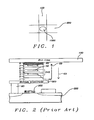
- Fig. 1 is a highly schematic drawing showing an overhead view of a conventional MRAM cell comprising an MTJ cell element (1000) positioned between (or at the intersection of) vertically separated orthogonal word (200) and bit (100) lines.
- the cell element (1000) is drawn with a slightly elliptical horizontal cross-section because such an anisotropic shape ("shape anisotropy") produces a corresponding magnetic anisotropy within the free layer that assists its magnetic moment in retaining a thermally stable fixed position after switching fields have been turned off.
- the direction along the free layer in which it is energetically favorable for the moment to remain and from which it should be difficult to switch the magnetic moment unintentionally (as with thermal effects), the longer direction in this case, is called the “easy axis" of the layer.
- the axis perpendicular to the easy axis is called the “hard axis.”
- the fields produced by currents in each of the two lines are between about 30 to 60 Oersteds in magnitude. According to the diagram, the word line field will be along the easy axis of the cell element, the bit line field will be along the easy axis.
- a spin transfer device described by Slonczewski, (US Patent No. 5,695,164 ) and Covington (US Patent No. 7,006,375 ), has been developed, that seems to eliminate some of the problems associated with the excessive power consumption necessitated by external switching fields.
- the spin transfer device shares some of the operational features of the conventional MTJ cell (particularly the read process) described above, except that the switching of the free layer magnetic moment (the write process) is produced by passage of the spin polarized current itself.
- unpolarized conduction electrons passing through a first magnetic layer having its magnetic moment oriented in a given direction are preferentially polarized by their passage through that layer by a quantum mechanical exchange interaction with the polarized bound electrons in the layer.
- a polarization can occur to conduction electrons that reflect from the surface of the magnetized layer as well as to those that pass through it. The efficiency of such a polarization process depends upon the crystalline structure of the layer.
- FIG. 2 there is shown a schematic illustration of an exemplary prior art MTJ cell element (such as that in Fig. 1 ) being contacted from above by a bit line (100) and from below by a bottom electrode (300).
- the bottom electrode is in electrical contact, through a conducting via (80), with a CMOS transistor (500) that provides current to the MTJ element when the element is selected in a read or write operation.
- CMOS transistor 500
- this prior art storage device consists of an underlayer (1), which could be a seed layer or buffer layer, an antiferromagnetic pinning layer (2), a synthetic antiferromagnetic (SyAF) pinned reference layer (345), consisting of a first ferromagnetic layer (3), a non-magnetic spacer layer (4) and a second ferromagnetic layer (5), a non-conducting tunneling barrier layer (6), a ferromagnetic free layer (7) and a non-magnetic capping layer (8).
- Arrows, (20) and (30) indicate the antiparallel magnetization directions of the two ferromagnetic layers (3) and (5) of the SyAF pinned layer (345).
- the double-headed arrow (40) in free layer (7) indicates that this layer is free to have its magnetic moment directed in either of two directions.
- the free layer magnetization (40) would be switched, by torque transfer of angular momentum, to the same direction as that of the pinned reference layer's direction (30), since the conduction electrons have passed through that layer before entering the free layer.
- the MTJ element is then in its low resistance state.
- this entire configuration represents a schematic diagram of a single spin-RAM memory cell that utilizes the spin transfer effect (denoted hereinafter as an STT-RAM) for switching an MTJ type element.
- element to describe the basic MTJ structure comprising a tunneling barrier layer sandwiched between ferromagnetic fixed and free layers.
- memory cell to denote the combination of the MTJ element incorporated within the circuitry shown that permits the element to be written on and read from.
- Such circuitry includes intersecting current carrying lines that allow a particular element to be accessed and also a CMOS transistor that allows a current to be injected into the element.
- the word line provides the bit selection (i.e., selects the particular cell which will be switched by means of a current passing through it between the bit line and the source line) and the transistor provides the current necessary for switching the MTJ free layer of the selected cell.
- the cell is read by applying a bias voltage between the bit line and source line, thereby measuring its resistance and comparing that resistance with a standard cell in the circuit (not shown).
- the corresponding critical current density, J c which is I c /A, is on the order of several 10 7 Amperes/cm 2 .
- This high current density which is required to induce the spin transfer effect, could destroy the insulating tunneling barrier in the MTJ cell, such as a layer of AIOx, MgO, etc.
- the difference between an STT-RAM and a conventional MRAM is only in the write operation mechanism; the read operation is the same for both types of cell.
- the critical current density must be lower than 10 6 A/cm 2 if it is to be driven by a CMOS transistor that can typically deliver 100 ⁇ A per 100 nm of gate width.
- Such MRAM-MTJ cells have a dR/R ⁇ 40%.
- R p covariance indicates the statistical spread of R p values.
- R p is as defined above and R ap is the MTJ resistance when the free and pinned layers have their magnetizations aligned in an antiparallel configuration.
- Uniformity of the TMR ratio and the absolute resistance of the cell are critical to the success of MRAM architecture since the absolute value of the MTJ resistance is compared to the resistance of a reference cell during the read operation. If the active device resistances in a block of memory show a high variation in resistance (i.e. high R p covariance, or R ap covariance), a signal error can occur when they are compared with the reference cell.
- TMR/(R p covariance) should have a minimum value of 12 and most preferably be >20.
- J c 2 ⁇ e ⁇ ⁇ M s ⁇ t F ⁇ H a + H k + 2 ⁇ ⁇ ⁇ M s / ⁇
- e the electron charge
- ⁇ the Gilbert damping constant
- t F the free layer thickness
- ⁇ the reduced Planck's constant
- ⁇ the spin-transfer efficiency (related to the tunneling spin polarization factor of the incident spin-polarized current)
- H a is the external applied field
- H k is the uniaxial anisotropy field
- 2 ⁇ M s is the demagnetization field of the free layer.
- M. Hosami (A novel nonvolatile memory with spin torque transfer magnetization switching: Spin RAM” 2005 IEDM, paper 19-1), discusses a Spin-RAM 4Kbit array which is fabricated using a stack of the following form: CoFeB/RF-sputtered MgO/CoFeB with a MnPt pinning layer. This MTJ stack is processed using 350°C, 10KOe annealing. The cell size is a 100nm x 150nm oval. Patterning of such sub 100 nm oval MTJ elements is done using e-beam lithography.
- the tunnel barrier layer is (001) crystallized MgO whose thickness is less than 10 x 10 -10 meters for the desired RA of about 20 ⁇ - ⁇ m 2 .
- Intrinsic dR/R of the MTJ is 160%, although under operational conditions (0.1 V bias, for read determination) it is about 100%.
- the critical current density is about 2.5 x 10 6 A/cm 2 .
- the distribution of write voltages for the array, for the high resistance state to the low resistance state has shown a good write margin.
- Resistance distributions for the high and low resistance states has a sigma (R p covariance) around 4%.
- TMR/ R p covariance is 25.
- Intrinsic MR as a function of the annealing temperature for an MTJ stack formed of Co 40 Fe 40 B 20 /MgO/ Co 40 Fe 40 B 20 with a 20 x 10 -10 meters thick Co 40 Fe 40 B 20 free layer are 49, 73 and 110% respectively. It is noted that the free layer in an MTJ processed at 270 and 300° annealing temperatures is amorphous.
- the pinning layer for the MTJ stack was IrMn.
- the free layer of the dual structure is made of a low saturation moment (approx. 1000 x 10 2 A/m) amorphous CoFeB.
- the nominal MTJ size is 90 nm x 140 nm.
- RA is about 20 ⁇ - ⁇ m 2 and dR/R is about 20%.
- DSF dual spin-filter
- Horng et al. US Patent Application US 2008/0179699 (docket No. HMG06-042. "A novel MTJ to reduce spin-transfer magnetization switching current") is assigned to the same assignee (Magic Technologies) as the present invention and fully incorporated herein by reference.
- Horng et al. have produced an STT-MTJ test structure that includes a MTJ stack of the form: Ta/NiCr/MnPt/Co 75 Fe 25 /Ru7.5/Co 60 Fe 20 B 20 -Co 75 Fe 25 /(NOX)MgO11/ Co 60 Fe 20 B 20 /Ta
- the pinning layer is MnPt.
- RA of the MTJ is controlled to less than 10 ⁇ - ⁇ m 2 and intrinsic dR/R is about 100%.
- dR/R at 0.1 V bias is about 70-80%. Due to the fact that no array was constructed, there was no determination of R p covariance. However, the covariance for a conventional MRAM of the same basic MTJ structure, but 200 nm x 325 nm was measured to about 3.5%. Extrapolation to the 100 nm x 150 nm size of the STT-MTJ predicts that the covariance would be about 7 %. This value would not be sufficient to provide a good read margin.
- the TMR sensor currently under production at Headway Technologies uses an MTJ element of the form: Ta/Ru/IrMn/CoFe/Ru/CoFeB/CoFe/MgO/CoFe-NiFe/NiFeHf
- the pinning layer is IrMn.
- TMR sensor size when the resistance measurements are made is 100 nm x 500 nm. Patterning is done using conventional photo-lithography of the 180 nm node technology. R p covariance across the 6" wafer for that sensor size is about 3%. Scaling to a 100 nm x 150 nm size, the covariance is projected to be about 5%.
- a first AFM layer is preferably IrMn.
- Huai et al. discloses that an AFM layer is preferably IrMn or PtMn.
- Huai et al. (US Patent No. 7,106,624 ) states that the AFM is preferably PtMn but "nothing prevents" the use of IrMn instead.
- Covington (US Patent No. 7,006,375 ) shows a pinned layer that can be either IrMn or PtMn.
- Pakala et al. discloses that seed layers may be used to provide a desired texture to the AFM layer. For example, if IrMn is used as the AFM layer, then a TaN layer should be used.
- US 2007 / 0096229 discloses a magnetoresistive element including a magnetic recording layer which records information as a magnetization direction changes upon supplying a bidirectional current ill an out-of-plane direction, a magnetic reference layer which has a fixed magnetization direction, and a nonmagnetic layer which is provided between the magnetic recording layer and the magnetic reference layer.
- the magnetic recording layer includes an interface magnetic layer which is provided in contact with the nonmagnetic layer and has a first magnetic anisotropy energy, and a magnetic stabilizing layer which has a second magnetic anisotropy energy higher than the first magnetic anisotropy emery.
- US 2006 / 0152861 discloses a tunneling magneto-resistive spin valve sensor wherein the conventional free layer in a TMR read head has been replaced by a composite of two or more magnetic layers, one of which is iron rich
- the present invention will describe a spin transfer MRAM device in which a new form of free layer, combined with an IrMn pinning layer will address the issues raised above in statements 1-4.
- a first object of the present invention is to provide an MTJ element for an STT-MRAM cell wherein the critical current for magnetization switching by spin-torque transfer (STT) is lowered.
- a second object of this invention is to provide a MTJ element for an STT-RAM configured MRAM device in which the intrinsic (unbiased) and operational (biased) TMR ratio, dR/R, is significantly enhanced and wherein the intrinsic dR/R is between about 125% to 130%.
- a third object of the present invention is to provide such a device in which the product RA, of MTJ resistance (R) and MTJ element cross-sectional area (A) is less than a certain amount, preferably less than 10 ⁇ - ⁇ m 2 ,
- a fourth object of the present invention is to provide a MTJ element patterned using standard 180 nm photo-lithography and corresponding STT-RAM configured MRAM array of such elements, wherein the statistical distribution of MTJ resistances has a low covariance, preferably less than 5%.
- a fifth object of the present invention is to provide a MTJ element and corresponding STT-RAM configured MRAM array of such elements, wherein the read margin, (TMR/R p covariance), is greater than 15, and for an element of cross-sectional area 100 nm x 150 nm is at least 20.
- a sixth object of the present invention is to provide such an MTJ element wherein the structure of the pinning/pinned layer provides a low angular dispersion of the pinned layer magnetic moment direction, preferably 1.6X less than that of conventional configurations.
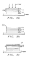
- the preferred structure of the MTJ element is of the form:
- the free layer is of the form Fe 3/CoFeB 20/Fe 6, with the two interfacial Fe layers being very thin (respectively 3 and 6 x 10 -10 meters (angstroms) and crystalline in structure for enhanced spin polarization of the current, while the CoFeB layer sandwiched between them is amorphous in form to obtain a low Gilbert magnetic damping factor.
- the tunneling barrier layer is a layer of MgO that is rendered crystalline in nature by being formed by a combination of a sputtering deposition of Mg and a natural oxidation process.
- the sputtering is onto an exposed surface of AP1 that has been preconditioned by a plasma treatment to render it smooth/flat.
- This plasma pretreatment is, in turn, highly advantageous, given the fact that the pinning layer for the SyAF pinned layer is a layer of Mnlr rather than the more usual MnPt.
- the MnIr pinning layer allows an advantageous annealing process in which the anneal need only be carried out at 265°C for between 1 and 2 hours in a magnetic field of 795,77 K Ampere per meter (10 K Oe).
- other prior art processes form the MgO tunneling barrier layer by sputtering directly from an MgO target. This produces an amorphous layer which must be rendered crystalline by use of much higher annealing temperatures than are required in the present invention.
- the preferred embodiment of the present invention is an STT-RAM memory cell and an array of such cells, in which each cell incorporates an MTJ element that operates in the spin torque transfer (STT) mode.
- the MTJ element includes an IrMn pinning layer, an SyAF pinned layer, a crystalline barrier layer of naturally oxidized MgO and a crystalline-Fe-sandwiched CoFeB free layer having Gilbert damping constants that are lower than those associated with free layers of only amorphous CoFeB.
- the preferred MTJ stack configuration is: BE/NiCr50/Ru20/MnIr70/Co 75 Fe 25 23(AP2)/Ru7.5/CoFeB 20 -Co 75 Fe 25 6-7 (AP1)/PT/ Mg8-NOX-Mg4/Fe3-Co 60 Fe 20 B 20 20-Fe6(FL)/Ta
- a bottom conducting line or electrode 300
- Layer (1) is a layer of NiCr, which is a seed layer.
- Layer (2) is the pinning layer, which is a layer of MnIr of 70 x 10 -10 meters thickness.
- Layer (345) is the configuration Co 75 Fe 25 23(AP2)/Ru7.5/CoFeB 20 - Co 75 Fe 25 6-7 (AP1) is a synthetic antiferromagnetic (SyAF) pinned layer, where AP1 (5) and AP2 (3) denote the two ferromagnetic layers magnetized in antiparallel directions and exchange coupled by the layer of Ru (4).
- PT denotes a plasma treatment (55) that is applied to the upper surface of AP1 and is required to produce the desired objects of the invention.
- Fig. 3b there is shown the formation of an MgO (or, similarly, an AIOx) barrier layer (6) on the plasma treated surface (555) of AP1.
- the plasma treatment which smoothes and renders flat the (555) surface, is required because layers formed on a MnIr/SyAF combination such as in the present invention are typically rougher than when formed on an MnPt /SyAF combination. Consequently, dR/R and He (H in ) pf the Mnlr MTJ are not as good as that for the MnPt MTJ.
- the CoFe(B)/MgO/CoFeB interfaces must be smooth.
- PT plasma treatment
- the MgO barrier layer (6) is made by a process indicated above by Mg8-NOX-Mg4 and which is more fully described by Horng et al cited above.
- a target of MgO is sputtered and thereby produces an amorphous MgO layer
- an Mg target is sputtered to produce a crystalline Mg layer and that already crystalline layer is then naturally oxidized after deposition to directly produce a crystalline MgO layer.
- a subsequent second Mg sputtering process completes the layer formation as described by Horng. In its as-deposited state, the naturally oxidized Mg already has a highly oriented (001) crystalline plane texture.
- the free layer (7) of the configuration above is a composite layer made of an atomic layer thickness (approximately 3 x 10 -10 meters) crystalline Fe interface layer (71) and thicker, amorphous layer (72) of Co 60 Fe 20 B 20 (approximately 20 x 10 -10 meters) formed upon it. More preferably, as is shown in the figure, an additional crystalline layer (73) of Fe approximately 6 x 10 -10 meters in thickness can be inserted between the Co 60 Fe 20 B 20 and the Ta 30 capping layer (8).
- FIG. 4 there is seen a table setting forth the magnetic properties of 7 MTJ stack configurations having the general form: Buffer layer/Pinning layer//Co 75 Fe 25 23/Ru7.5/Co 60 Fe 20 B 20 15-Co 75 Fe 25 (AP1)/Mg8NOX-Mg4/Fee layer/Ta30/Ru
- Row 1 shows the properties of the reference MTJ stack in which the pinning layer is MnPt and the free layer lacks the Fe crystalline layer and consists only of the amorphous CoFeB layer.
- Row 3 shows a similar structure except that the pinning layer is Mnlr and the free layer includes the crystalline Fe layer.
- MR for row 1 is 103%, while for row 3 it is 118%. This improvement is attributed to the (001) Fe crystalline interface layer in the free layer structure.
- H e (H in ) for the MnIr-MTJ is 7.60 Oe, a twofold increase over the value of 3.73 Oe for the MnPt MTJ of the reference structure.
- Row 2 and Row 4 which include a 120 s plasma treatment (PT) of the AP1 surface, show that H e of both the MnPt and Mnlr TMJ have been reduced to 2.48 and 4.41 Oe respectively. Having smooth/flat interfaces at the AP1/MgO/free layer enhances the MR for both the MnPt and MnIr structures.
- MR at 0.1 V bias read operation
- the covariance would have to be less than or equal to 5%.
- the deposited MTJ stack is annealed using a 265°C (1-2 h)10K Oe process.
- post deposition annealing to the MTJ stack was done in a 280°C (5 h)-10 K Oe process.
- Post deposition annealing for the MnIr/SyAF MTJ is at 250°-265°C (5 h)- 10 K Oe.
- the 265°C (1-2 h)10K Oe process is more suitable for the Mnlr pinning layer structure than for the MnPt pinning structure.
- the MnIr MTJ element is preferred.
- Fig's 5a and 5b there is shown the B-H characteristic plots for the MTJ element made (in 5a) for the MnPt pinning layer and (5b) for the MnIr pinning layer.
- the open loop portion of each curve (arrows) allows us to deduce the pinned layer dispersion and the strength of the pinning field for the Mnlr MTJ and for the MnPt MTJ.
- the ratio of H pin (MnIr)/H pin (MnPt) is approximately 1.6.
- the ratio of dispersion (MnPt)/dispersion (MnIr) is about 1.6. From this, we can also deduce that the covariance ratio of [R p cov.
- the boron (B) doping to the CoFe free layer has enhanced the magnetization damping.
- Use of the Fe crystalline interface layers provides high spin polarization (higher than from the amorphous CoFeB layer alone).
Landscapes
- Engineering & Computer Science (AREA)
- Chemical & Material Sciences (AREA)
- Nanotechnology (AREA)
- Crystallography & Structural Chemistry (AREA)
- Power Engineering (AREA)
- Manufacturing & Machinery (AREA)
- Physics & Mathematics (AREA)
- General Physics & Mathematics (AREA)
- Condensed Matter Physics & Semiconductors (AREA)
- Computer Hardware Design (AREA)
- Spectroscopy & Molecular Physics (AREA)
- Hall/Mr Elements (AREA)
- Mram Or Spin Memory Techniques (AREA)
Claims (13)
- STT-MTJ MRAM-Zelle, die in einer CPP-Konfiguration betrieben wird, und mittels eines Drehmoments eine Übertragung eines Leitungselektronenspindrehimpulses verwendet, um eine Magnetisierungsrichtung einer freien Schicht zu ändern, aufweisend:ein Substrat;ein MTJ-Element, das auf dem Substrat ausgebildet ist, wobei das Element eine vertikal gestapelte Beschichtung von horizontalen, parallelen Schichten aufweist, gekennzeichnet durch:eine antiferromagnetische Pinningschicht (2), die auf MnIr ausgebildet ist,eine durch ein Plasmaverfahren hergestellte SyAF Pinningschicht (345), um eine glatte/ebene Grenzfläche zu haben,eine Tunnelbarrierenschicht (6), die auf der glatten/ebenen Grenzfläche ausgebildet ist, wobei die Tunnelbarrierenschicht eine inherente kristalline Struktur hat, die kein weiteres Tempern erfordert, und eine natürlich oxidierte, erste gesputterte Schicht auf Mg aufweist, auf welcher eine zweite, gesputterte Schicht auf MG ausgebildet ist,eine ferromagnetische, freie Schicht (7), die auf der Tunnelbarrierenschicht ausgebildet ist, wobei die ferromagnetische, freie Schicht einen niedrigen magnetischen Dämpfungsfaktor aufweist und eine verbesserte Polarisierung der Leitungselektronen erzeugt,
wobeidie ferromagnetische, freie Schicht eine Beschichtung ist, die ferner eine erste Grenzflächenschicht (71) aus kristallinem Fe aufweist, auf der eine amorphe ferromagnetische Schicht (72) ausgebildet ist, auf der eine zweite Grenzflächenschicht (73) aus Fe ausgebildet ist. - Zelle nach Anspruch 1, wobei die kristalline Schicht aus Fe etwa 3 x 10⁻¹⁰ m dick ist, und wobei die amorphe, ferromagnetische Schicht eine Schicht aus Co60Fe20B20 von etwa 20 x 10-10 m Dicke ist, und wobei die zweite kristalline Schicht aus Fe etwa 6 x 10⁻¹⁰ m dick ist.
- Zelle nach Anspruch 2, wobei die amorphe, ferromagnetische Schicht eine Schicht aus Co60Fe20B20 mit einer Dicke von 15 x 10-10 m ist.
- Zelle nach Anspruch 2 oder 3, wobei die kristallinen Schichten aus Fe jeweils mit einer (001) Kristallebene parallel zu ihrer Ausbildungsebene ausgebildet sind.
- Zelle nach Anspruch 1, wobei die Tunnelbarrierenschicht eine kristalline Schicht aus natürlich oxidiertem, gesputterten Mg ist, die bis zu einer Dicke von etwa 12 x 10-10 m ausgebildet ist.
- Zelle nach Anspruch 1, wobei die Pinningschicht aus IrMn mit bis zu einer Dicke von etwa 70 x 10-10 m ausgebildet ist.
- Zelle nach Anspruch 1, wobei die SyAF Pinningschicht eine Schicht aus Co75Fe25 aufweist, die bis zu einer Dicke von etwa 23 x 10-10 m ausgebildet ist, auf der eine Schicht aus Ru mit einer Dicke von etwa 7,5 x 10⁻¹⁰ m ausgebildet ist, auf der eine Doppelschicht ausgebildet ist, aufweisend eine Schicht aus Co60Fe20B20 von etwa 15 x 10-10 m Dicke, auf der eine Schicht aus Co75Fe25 von zwischen ungefähr 6 x 10⁻¹⁰ m und 7 x 10⁻¹⁰ m Dicke ausgebildet ist.
- Zelle nach Anspruch 1, wobei das Substrat eine untere Elektrode ist, und wobei die Abdeckschicht elektrisch durch eine Bitleitung kontaktiert ist.
- Verfahren zur Ausbildung einer STT-MTJ MRAM-Zelle, die in einer CPP-Konfiguration betrieben wird, und mittels eines Drehmoments eine Übertragung eines Leitungselektronenspindrehimpulses verwendet, um eine Magnetisierungsrichtung einer freien Schicht zu ändern, aufweisend:Bereitstellen eines Substrats;Ausbilden eines MTJ-Elements auf dem Substrat, wobei das Element eine vertikal gestapelte Beschichtung von horizontalen, parallelen Schichten aufweist, die nach den folgenden Verfahrensschritten und in der folgenden Reihenfolge hergestellt ist, und gekennzeichnet ist durch:Ausbilden einer antiferromagnetischen Pinningschicht (2) auf Mnlr, dann Ausbilden einer SyAF Pinningschicht (345) auf der Pinningschicht, dann Anwenden eines Plasmaverfahrens auf eine ausgesetzte obere Oberfläche der SyAF Pinningschicht, wobei das Plasmaverfahren eine glatte/ebene obere Oberfläche erzeugt, dannAusbilden einer Tunnelbarrierenschicht (6) aus MgO auf der glatten und ebenen oberen Oberfläche, wobei die Tunnelbarrierenschicht mit einem Verfahren ausgebildet wird,welches das Sputtern einer ersten Schicht aus kristallinem Mg, dann Erzeugen seiner natürlichen Oxidation, und dann Sputtern einer zweiten Schicht aus kristallinem Mg aufweist, wodurch die Tunnelbarrierenschicht direkt in einem kristallinen Zustand ausgebildet wird; dannAusbilden einer ferromagnetischen, freien Schicht (7) auf der kristallinen Schicht aus MgO, wobei die freie Schicht eine erste Schicht (71) aus kristallinem Fe, auf der eine Schicht (72) aus amorphem ferromagnetischen Material ausgebildet ist, auf der eine zweite Schicht (73) aus kristallinem Fe ausgebildet ist, wobei die Schichten aus kristallinem Fe eine kristalline Struktur aufweisen, welche mit der kristallinen Struktur der Barrierenschicht übereinstimmt, und wobei die Schicht aus amorphem ferromagnetischen Material einen niedrigen magnetischen Dämpfungsfaktor hat, dann Ausbilden einer Abdeckschicht (8) auf der dritten ferromagnetischen Schicht und Behandeln der Anordnung mit einer Verfahrenstemperatur und mit einem Verfahrens-Magnetfeld und mit einer Verfahrenszeit, um die zweite ferromagnetische Schicht ins Amorphe umzuwandeln, während gleichzeitig nicht die Schicht Mnlr negativ beeinflusst wird, und eine Magnetfeldausrichtung der Pinningschicht und der freien Schichten festgelegt wird.
- STT-MTJ MRAM-Zelle, die in einer CPP-Konfiguration betrieben wird, und mittels eines Drehmoments eine Übertragung eines Leitungselektronenspindrehimpulses verwendet, um eine Magnetisierungsrichtung einer freien Schicht zu ändern, aufweisend:ein Substrat;ein MTJ-Element, das auf dem Substrat ausgebildet ist, wobei das Element eine vertikal gestapelte Beschichtung von horizontalen, parallelen Schichten aufweist,
gekennzeichnet durch:eine antiferromagnetische Pinningschicht (2), die auf MnIr ausgebildet ist,eine durch ein Plasmaverfahren hergestellte SyAF Pinningschicht (345), um eine glatte/ebene Grenzfläche zu haben,eine Tunnelbarrierenschicht (6), die auf der glatten/ebenen Grenzfläche ausgebildet ist,wobei die Tunnelbarrierenschicht eine inherente kristalline Struktur hat, die kein weiteres Tempern erfordert, und eine natürlich oxidierte, erste gesputterte Schicht auf Mg aufweist, auf welcher eine zweite, gesputterte Schicht auf MG ausgebildet ist,eine ferromagnetische, freie Schicht (7), die auf der Tunnelbarrierenschicht ausgebildet ist, wobei die ferromagnetische, freie Schicht einen niedrigen magnetischen Dämpfungsfaktor aufweist und eine verbesserte Polarisierung der Leitungselektronen erzeugt, wobeidie ferromagnetische, freie Schicht (7) eine Doppelbeschichtung ist, die kristalline Schicht einer binären Legirun aus Fe, reich an FeCo, auf der eine kristalline Schicht aus einer binären Legierung von Fe, reich an FeNi, ausgebildet ist. - Zelle nach Anspruch 10, wobei die Tunnel barrierenschicht eine Schicht aus natürlich oxidiertem, gesputterten Mg ist, die bis zu einer Dicke von etwa 12 x 10-10 m ausgebildet ist.
- Zelle nach Anspruch 10, wobei die Pinningschicht aus IrMn mit bis zu einer Dicke von etwa 70 x 10-10 m ausgebildet ist.
- Zelle nach Anspruch 10, wobei die SyAF Pinningschicht eine Schicht aus Co75Fe25 aufweist, die bis zu einer Dicke von etwa 23 x 10-10 m ausgebildet ist, auf der eine Schicht aus Ru mit einer Dicke von etwa 7,5 x 10⁻¹⁰ m ausgebildet ist, auf der eine Doppelschicht ausgebildet ist, aufweisend eine Schicht aus Co60Fe20B20 von etwa 15 x 10-10 m Dicke, auf der eine Schicht aus Co75Fe25 von zwischen ungefähr 6 x 10⁻¹⁰ m und 7 x 10⁻¹⁰ m Dicke ausgebildet ist.
Applications Claiming Priority (1)
| Application Number | Priority Date | Filing Date | Title |
|---|---|---|---|
| US11/880,583 US7750421B2 (en) | 2007-07-23 | 2007-07-23 | High performance MTJ element for STT-RAM and method for making the same |
Publications (3)
| Publication Number | Publication Date |
|---|---|
| EP2073285A2 EP2073285A2 (de) | 2009-06-24 |
| EP2073285A3 EP2073285A3 (de) | 2012-10-17 |
| EP2073285B1 true EP2073285B1 (de) | 2015-04-29 |
Family
ID=40295118
Family Applications (1)
| Application Number | Title | Priority Date | Filing Date |
|---|---|---|---|
| EP20080392010 Active EP2073285B1 (de) | 2007-07-23 | 2008-07-09 | Hochleistungs-MTJ-Element für STT-RAM und Herstellungsverfahren dafür |
Country Status (3)
| Country | Link |
|---|---|
| US (4) | US7750421B2 (de) |
| EP (1) | EP2073285B1 (de) |
| JP (1) | JP5279384B2 (de) |
Families Citing this family (220)
| Publication number | Priority date | Publication date | Assignee | Title |
|---|---|---|---|---|
| US8755222B2 (en) | 2003-08-19 | 2014-06-17 | New York University | Bipolar spin-transfer switching |
| US7911832B2 (en) * | 2003-08-19 | 2011-03-22 | New York University | High speed low power magnetic devices based on current induced spin-momentum transfer |
| JP2007052886A (ja) * | 2005-08-19 | 2007-03-01 | Alps Electric Co Ltd | 垂直磁気記録ヘッド |
| JP2007095750A (ja) * | 2005-09-27 | 2007-04-12 | Canon Anelva Corp | 磁気抵抗効果素子 |
| FR2892871B1 (fr) * | 2005-11-02 | 2007-11-23 | Commissariat Energie Atomique | Oscillateur radio frequence a courant elelctrique polarise en spin |
| US7710687B1 (en) * | 2006-09-13 | 2010-05-04 | Hutchinson Technology Incorporated | High conductivity ground planes for integrated lead suspensions |
| US20080088983A1 (en) * | 2006-10-11 | 2008-04-17 | Gereon Meyer | Damping control in magnetic nano-elements using ultrathin damping layer |
| US8089723B2 (en) * | 2006-10-11 | 2012-01-03 | Hitachi Global Storage Technologies Netherlands B.V. | Damping control in magnetic nano-elements using ultrathin damping layer |
| US7695761B1 (en) | 2006-12-21 | 2010-04-13 | Western Digital (Fremont), Llc | Method and system for providing a spin tunneling magnetic element having a crystalline barrier layer |
| US8559141B1 (en) | 2007-05-07 | 2013-10-15 | Western Digital (Fremont), Llc | Spin tunneling magnetic element promoting free layer crystal growth from a barrier layer interface |
| JP4435207B2 (ja) * | 2007-06-13 | 2010-03-17 | 株式会社東芝 | 磁気ランダムアクセスメモリ |
| US20090046397A1 (en) * | 2007-08-15 | 2009-02-19 | Freescale Semiconductor, Inc. | Methods and apparatus for a synthetic anti-ferromagnet structure with improved thermal stability |
| US9812184B2 (en) | 2007-10-31 | 2017-11-07 | New York University | Current induced spin-momentum transfer stack with dual insulating layers |
| US8094421B2 (en) * | 2007-12-26 | 2012-01-10 | Hitachi Global Storage Technologies Netherlands, B.V. | Current-perpendicular-to-plane (CPP) read sensor with multiple reference layers |
| US8545999B1 (en) * | 2008-02-21 | 2013-10-01 | Western Digital (Fremont), Llc | Method and system for providing a magnetoresistive structure |
| KR101586271B1 (ko) * | 2008-04-03 | 2016-01-20 | 삼성전자주식회사 | 자기 메모리 소자 및 그 정보 쓰기 및 읽기 방법 |
| US7760542B2 (en) | 2008-04-21 | 2010-07-20 | Seagate Technology Llc | Spin-torque memory with unidirectional write scheme |
| US8659852B2 (en) | 2008-04-21 | 2014-02-25 | Seagate Technology Llc | Write-once magentic junction memory array |
| US7852663B2 (en) * | 2008-05-23 | 2010-12-14 | Seagate Technology Llc | Nonvolatile programmable logic gates and adders |
| US7855911B2 (en) * | 2008-05-23 | 2010-12-21 | Seagate Technology Llc | Reconfigurable magnetic logic device using spin torque |
| US8081405B2 (en) * | 2008-05-29 | 2011-12-20 | Hitachi Global Storage Technologies Netherlands, B.V. | Current-perpendicular-to-plane (CPP) read sensor with smoothened multiple reference layers |
| US8116122B2 (en) * | 2008-06-27 | 2012-02-14 | Seagate Technology Llc | Spin-transfer torque memory self-reference read method |
| US8116123B2 (en) * | 2008-06-27 | 2012-02-14 | Seagate Technology Llc | Spin-transfer torque memory non-destructive self-reference read method |
| US8233319B2 (en) * | 2008-07-18 | 2012-07-31 | Seagate Technology Llc | Unipolar spin-transfer switching memory unit |
| US8274818B2 (en) * | 2008-08-05 | 2012-09-25 | Tohoku University | Magnetoresistive element, magnetic memory cell and magnetic random access memory using the same |
| US7881098B2 (en) * | 2008-08-26 | 2011-02-01 | Seagate Technology Llc | Memory with separate read and write paths |
| JP2010062353A (ja) * | 2008-09-04 | 2010-03-18 | Fujitsu Ltd | 磁気抵抗効果素子 |
| US7826255B2 (en) * | 2008-09-15 | 2010-11-02 | Seagate Technology Llc | Variable write and read methods for resistive random access memory |
| US8482966B2 (en) * | 2008-09-24 | 2013-07-09 | Qualcomm Incorporated | Magnetic element utilizing protective sidewall passivation |
| US9929211B2 (en) * | 2008-09-24 | 2018-03-27 | Qualcomm Incorporated | Reducing spin pumping induced damping of a free layer of a memory device |
| US7985994B2 (en) | 2008-09-29 | 2011-07-26 | Seagate Technology Llc | Flux-closed STRAM with electronically reflective insulative spacer |
| US7933137B2 (en) * | 2008-10-08 | 2011-04-26 | Seagate Teachnology Llc | Magnetic random access memory (MRAM) utilizing magnetic flip-flop structures |
| US8169810B2 (en) * | 2008-10-08 | 2012-05-01 | Seagate Technology Llc | Magnetic memory with asymmetric energy barrier |
| US7933146B2 (en) * | 2008-10-08 | 2011-04-26 | Seagate Technology Llc | Electronic devices utilizing spin torque transfer to flip magnetic orientation |
| US8039913B2 (en) * | 2008-10-09 | 2011-10-18 | Seagate Technology Llc | Magnetic stack with laminated layer |
| US8089132B2 (en) | 2008-10-09 | 2012-01-03 | Seagate Technology Llc | Magnetic memory with phonon glass electron crystal material |
| US7966581B2 (en) * | 2008-10-16 | 2011-06-21 | Seagate Technology Llc | Generic non-volatile service layer |
| US20100102405A1 (en) * | 2008-10-27 | 2010-04-29 | Seagate Technology Llc | St-ram employing a spin filter |
| US8045366B2 (en) | 2008-11-05 | 2011-10-25 | Seagate Technology Llc | STRAM with composite free magnetic element |
| US8043732B2 (en) | 2008-11-11 | 2011-10-25 | Seagate Technology Llc | Memory cell with radial barrier |
| US7826181B2 (en) * | 2008-11-12 | 2010-11-02 | Seagate Technology Llc | Magnetic memory with porous non-conductive current confinement layer |
| US8289756B2 (en) | 2008-11-25 | 2012-10-16 | Seagate Technology Llc | Non volatile memory including stabilizing structures |
| US8536669B2 (en) | 2009-01-13 | 2013-09-17 | Qualcomm Incorporated | Magnetic element with storage layer materials |
| US7826259B2 (en) * | 2009-01-29 | 2010-11-02 | Seagate Technology Llc | Staggered STRAM cell |
| US20100213073A1 (en) * | 2009-02-23 | 2010-08-26 | International Business Machines Corporation | Bath for electroplating a i-iii-vi compound, use thereof and structures containing same |
| US8120126B2 (en) * | 2009-03-02 | 2012-02-21 | Qualcomm Incorporated | Magnetic tunnel junction device and fabrication |
| US8587993B2 (en) | 2009-03-02 | 2013-11-19 | Qualcomm Incorporated | Reducing source loading effect in spin torque transfer magnetoresisitive random access memory (STT-MRAM) |
| US20100254174A1 (en) * | 2009-04-02 | 2010-10-07 | Seagate Technology Llc | Resistive Sense Memory with Complementary Programmable Recording Layers |
| US7969767B2 (en) * | 2009-05-29 | 2011-06-28 | Qualcomm Incorporated | Spin transfer torque—magnetic tunnel junction device and method of operation |
| US8381391B2 (en) | 2009-06-26 | 2013-02-26 | Western Digital (Fremont), Llc | Method for providing a magnetic recording transducer |
| US9171601B2 (en) | 2009-07-08 | 2015-10-27 | Alexander Mikhailovich Shukh | Scalable magnetic memory cell with reduced write current |
| US8406041B2 (en) | 2009-07-08 | 2013-03-26 | Alexander Mikhailovich Shukh | Scalable magnetic memory cell with reduced write current |
| US8331063B2 (en) | 2009-07-10 | 2012-12-11 | Tdk Corporation | Magnetoresistive effect element in CPP-type structure and magnetic disk device |
| US8154828B2 (en) | 2009-07-10 | 2012-04-10 | Tdk Corporation | Magnetoresistive effect element in CPP-type structure and magnetic disk device |
| US7999338B2 (en) | 2009-07-13 | 2011-08-16 | Seagate Technology Llc | Magnetic stack having reference layers with orthogonal magnetization orientation directions |
| US8609262B2 (en) * | 2009-07-17 | 2013-12-17 | Magic Technologies, Inc. | Structure and method to fabricate high performance MTJ devices for spin-transfer torque (STT)-RAM application |
| US8498084B1 (en) | 2009-07-21 | 2013-07-30 | Western Digital (Fremont), Llc | Magnetoresistive sensors having an improved free layer |
| US8194365B1 (en) | 2009-09-03 | 2012-06-05 | Western Digital (Fremont), Llc | Method and system for providing a read sensor having a low magnetostriction free layer |
| US8446753B2 (en) * | 2010-03-25 | 2013-05-21 | Qualcomm Incorporated | Reference cell write operations at a memory |
| US20110236723A1 (en) * | 2010-03-26 | 2011-09-29 | Tsann Lin | CURRENT-PERPENDICULAR-TO-PLANE (CPP) READ SENSOR WITH Co-Fe BUFFER LAYERS |
| WO2011121777A1 (ja) | 2010-03-31 | 2011-10-06 | 株式会社 東芝 | 磁気抵抗素子及び磁気メモリ |
| US8625337B2 (en) | 2010-05-06 | 2014-01-07 | Qualcomm Incorporated | Method and apparatus of probabilistic programming multi-level memory in cluster states of bi-stable elements |
| US8300356B2 (en) * | 2010-05-11 | 2012-10-30 | Headway Technologies, Inc. | CoFe/Ni Multilayer film with perpendicular anistropy for microwave assisted magnetic recording |
| US8604572B2 (en) * | 2010-06-14 | 2013-12-10 | Regents Of The University Of Minnesota | Magnetic tunnel junction device |
| US8907436B2 (en) | 2010-08-24 | 2014-12-09 | Samsung Electronics Co., Ltd. | Magnetic devices having perpendicular magnetic tunnel junction |
| US9299923B2 (en) | 2010-08-24 | 2016-03-29 | Samsung Electronics Co., Ltd. | Magnetic devices having perpendicular magnetic tunnel junction |
| JP5123365B2 (ja) * | 2010-09-16 | 2013-01-23 | 株式会社東芝 | 磁気抵抗素子及び磁気メモリ |
| US8358534B2 (en) | 2010-09-17 | 2013-01-22 | Micron Technology, Inc. | Spin torque transfer memory cell structures and methods |
| US8300454B2 (en) | 2010-09-17 | 2012-10-30 | Micron Technology, Inc. | Spin torque transfer memory cell structures and methods |
| US9666639B2 (en) | 2010-09-17 | 2017-05-30 | Micron Technology, Inc. | Spin torque transfer memory cell structures and methods |
| US8310868B2 (en) | 2010-09-17 | 2012-11-13 | Micron Technology, Inc. | Spin torque transfer memory cell structures and methods |
| JP5232206B2 (ja) * | 2010-09-21 | 2013-07-10 | 株式会社東芝 | 磁気抵抗素子及び磁気ランダムアクセスメモリ |
| US8760819B1 (en) | 2010-12-23 | 2014-06-24 | Western Digital (Fremont), Llc | Magnetic recording sensor with sputtered antiferromagnetic coupling trilayer between plated ferromagnetic shields |
| US8786036B2 (en) | 2011-01-19 | 2014-07-22 | Headway Technologies, Inc. | Magnetic tunnel junction for MRAM applications |
| US8325448B2 (en) | 2011-02-11 | 2012-12-04 | Headway Technologies, Inc. | Pinning field in MR devices despite higher annealing temperature |
| US20120241878A1 (en) * | 2011-03-24 | 2012-09-27 | International Business Machines Corporation | Magnetic tunnel junction with iron dusting layer between free layer and tunnel barrier |
| US9159908B2 (en) | 2011-05-05 | 2015-10-13 | Headway Technologies, Inc. | Composite free layer within magnetic tunnel junction for MRAM applications |
| US8686484B2 (en) | 2011-06-10 | 2014-04-01 | Everspin Technologies, Inc. | Spin-torque magnetoresistive memory element and method of fabricating same |
| US8462461B2 (en) * | 2011-07-05 | 2013-06-11 | HGST Netherlands B.V. | Spin-torque oscillator (STO) with magnetically damped free layer |
| US8492169B2 (en) | 2011-08-15 | 2013-07-23 | Magic Technologies, Inc. | Magnetic tunnel junction for MRAM applications |
| US8750031B2 (en) * | 2011-12-16 | 2014-06-10 | Taiwan Semiconductor Manufacturing Company, Ltd. | Test structures, methods of manufacturing thereof, test methods, and MRAM arrays |
| US9093639B2 (en) | 2012-02-21 | 2015-07-28 | Western Digital (Fremont), Llc | Methods for manufacturing a magnetoresistive structure utilizing heating and cooling |
| US8946834B2 (en) * | 2012-03-01 | 2015-02-03 | Headway Technologies, Inc. | High thermal stability free layer with high out-of-plane anisotropy for magnetic device applications |
| US9007818B2 (en) | 2012-03-22 | 2015-04-14 | Micron Technology, Inc. | Memory cells, semiconductor device structures, systems including such cells, and methods of fabrication |
| US10312433B2 (en) | 2012-04-06 | 2019-06-04 | Taiwan Semiconductor Manufacturing Company, Ltd | Reduction of capping layer resistance area product for magnetic device applications |
| US8923038B2 (en) | 2012-06-19 | 2014-12-30 | Micron Technology, Inc. | Memory cells, semiconductor device structures, memory systems, and methods of fabrication |
| US9054030B2 (en) | 2012-06-19 | 2015-06-09 | Micron Technology, Inc. | Memory cells, semiconductor device structures, memory systems, and methods of fabrication |
| US8852762B2 (en) | 2012-07-31 | 2014-10-07 | International Business Machines Corporation | Magnetic random access memory with synthetic antiferromagnetic storage layers and non-pinned reference layers |
| US20140037991A1 (en) | 2012-07-31 | 2014-02-06 | International Business Machines Corporation | Magnetic random access memory with synthetic antiferromagnetic storage layers |
| US8797692B1 (en) | 2012-09-07 | 2014-08-05 | Western Digital (Fremont), Llc | Magnetic recording sensor with AFM exchange coupled shield stabilization |
| US9082888B2 (en) | 2012-10-17 | 2015-07-14 | New York University | Inverted orthogonal spin transfer layer stack |
| US9082950B2 (en) | 2012-10-17 | 2015-07-14 | New York University | Increased magnetoresistance in an inverted orthogonal spin transfer layer stack |
| US9064534B1 (en) | 2012-11-30 | 2015-06-23 | Western Digital (Fremont), Llc | Process for providing a magnetic recording transducer with enhanced pinning layer stability |
| US8780505B1 (en) | 2013-03-12 | 2014-07-15 | Western Digital (Fremont), Llc | Method and system for providing a read transducer having an improved composite magnetic shield |
| US9379315B2 (en) | 2013-03-12 | 2016-06-28 | Micron Technology, Inc. | Memory cells, methods of fabrication, semiconductor device structures, and memory systems |
| GB2526456B (en) * | 2013-03-15 | 2020-07-15 | Intel Corp | Logic chip including embedded magnetic tunnel junctions |
| US20140295579A1 (en) * | 2013-03-29 | 2014-10-02 | T3Memory, Inc. | Method of patterning mtj stack |
| US9013836B1 (en) | 2013-04-02 | 2015-04-21 | Western Digital (Fremont), Llc | Method and system for providing an antiferromagnetically coupled return pole |
| US9070381B1 (en) | 2013-04-12 | 2015-06-30 | Western Digital (Fremont), Llc | Magnetic recording read transducer having a laminated free layer |
| US9431047B1 (en) | 2013-05-01 | 2016-08-30 | Western Digital (Fremont), Llc | Method for providing an improved AFM reader shield |
| US9361913B1 (en) | 2013-06-03 | 2016-06-07 | Western Digital (Fremont), Llc | Recording read heads with a multi-layer AFM layer methods and apparatuses |
| US8982613B2 (en) | 2013-06-17 | 2015-03-17 | New York University | Scalable orthogonal spin transfer magnetic random access memory devices with reduced write error rates |
| US9368714B2 (en) | 2013-07-01 | 2016-06-14 | Micron Technology, Inc. | Memory cells, methods of operation and fabrication, semiconductor device structures, and memory systems |
| US9466787B2 (en) | 2013-07-23 | 2016-10-11 | Micron Technology, Inc. | Memory cells, methods of fabrication, semiconductor device structures, memory systems, and electronic systems |
| US9293695B2 (en) | 2013-09-09 | 2016-03-22 | Koji Ueda | Magnetoresistive element and magnetic random access memory |
| US9299409B2 (en) * | 2013-09-11 | 2016-03-29 | Tadashi Miyakawa | Semiconductor storage device |
| US9461242B2 (en) | 2013-09-13 | 2016-10-04 | Micron Technology, Inc. | Magnetic memory cells, methods of fabrication, semiconductor devices, memory systems, and electronic systems |
| US9608197B2 (en) | 2013-09-18 | 2017-03-28 | Micron Technology, Inc. | Memory cells, methods of fabrication, and semiconductor devices |
| US9121886B2 (en) * | 2013-09-25 | 2015-09-01 | Seagate Technology Llc | Magnetoresistive sensor including an amorphous insertion layer excluding glass former elements |
| US9019754B1 (en) | 2013-12-17 | 2015-04-28 | Micron Technology, Inc. | State determination in resistance variable memory |
| US9147408B1 (en) | 2013-12-19 | 2015-09-29 | Western Digital (Fremont), Llc | Heated AFM layer deposition and cooling process for TMR magnetic recording sensor with high pinning field |
| US10454024B2 (en) | 2014-02-28 | 2019-10-22 | Micron Technology, Inc. | Memory cells, methods of fabrication, and memory devices |
| US9281466B2 (en) | 2014-04-09 | 2016-03-08 | Micron Technology, Inc. | Memory cells, semiconductor structures, semiconductor devices, and methods of fabrication |
| US9269888B2 (en) | 2014-04-18 | 2016-02-23 | Micron Technology, Inc. | Memory cells, methods of fabrication, and semiconductor devices |
| US9263667B1 (en) | 2014-07-25 | 2016-02-16 | Spin Transfer Technologies, Inc. | Method for manufacturing MTJ memory device |
| US9799382B2 (en) * | 2014-09-21 | 2017-10-24 | Samsung Electronics Co., Ltd. | Method for providing a magnetic junction on a substrate and usable in a magnetic device |
| US9337412B2 (en) | 2014-09-22 | 2016-05-10 | Spin Transfer Technologies, Inc. | Magnetic tunnel junction structure for MRAM device |
| US9349945B2 (en) | 2014-10-16 | 2016-05-24 | Micron Technology, Inc. | Memory cells, semiconductor devices, and methods of fabrication |
| US9768377B2 (en) | 2014-12-02 | 2017-09-19 | Micron Technology, Inc. | Magnetic cell structures, and methods of fabrication |
| US9437811B2 (en) * | 2014-12-05 | 2016-09-06 | Shanghai Ciyu Information Technologies Co., Ltd. | Method for making a magnetic random access memory element with small dimension and high quality |
| US10074387B1 (en) | 2014-12-21 | 2018-09-11 | Western Digital (Fremont), Llc | Method and system for providing a read transducer having symmetric antiferromagnetically coupled shields |
| US10439131B2 (en) | 2015-01-15 | 2019-10-08 | Micron Technology, Inc. | Methods of forming semiconductor devices including tunnel barrier materials |
| US20160276580A1 (en) * | 2015-03-20 | 2016-09-22 | Globalfoundries Singapore Pte. Ltd. | Bottom electrode for magnetic memory to increase tmr and thermal budget |
| US10128309B2 (en) | 2015-03-27 | 2018-11-13 | Globalfoundries Singapore Pte. Ltd. | Storage layer for magnetic memory with high thermal stability |
| US11114611B2 (en) * | 2015-04-03 | 2021-09-07 | Yimin Guo | Method to make MRAM with small footprint |
| US9728712B2 (en) | 2015-04-21 | 2017-08-08 | Spin Transfer Technologies, Inc. | Spin transfer torque structure for MRAM devices having a spin current injection capping layer |
| US10468590B2 (en) | 2015-04-21 | 2019-11-05 | Spin Memory, Inc. | High annealing temperature perpendicular magnetic anisotropy structure for magnetic random access memory |
| US9853206B2 (en) | 2015-06-16 | 2017-12-26 | Spin Transfer Technologies, Inc. | Precessional spin current structure for MRAM |
| US9537090B1 (en) | 2015-06-25 | 2017-01-03 | International Business Machines Corporation | Perpendicular magnetic anisotropy free layers with iron insertion and oxide interfaces for spin transfer torque magnetic random access memory |
| US11245069B2 (en) | 2015-07-14 | 2022-02-08 | Applied Materials, Inc. | Methods for forming structures with desired crystallinity for MRAM applications |
| US9773974B2 (en) | 2015-07-30 | 2017-09-26 | Spin Transfer Technologies, Inc. | Polishing stop layer(s) for processing arrays of semiconductor elements |
| US10163479B2 (en) | 2015-08-14 | 2018-12-25 | Spin Transfer Technologies, Inc. | Method and apparatus for bipolar memory write-verify |
| US10297745B2 (en) * | 2015-11-02 | 2019-05-21 | Globalfoundries Singapore Pte. Ltd. | Composite spacer layer for magnetoresistive memory |
| US10483320B2 (en) | 2015-12-10 | 2019-11-19 | Everspin Technologies, Inc. | Magnetoresistive stack with seed region and method of manufacturing the same |
| WO2017100547A1 (en) | 2015-12-10 | 2017-06-15 | Everspin Technologies, Inc. | Magnetoresistive stack, seed region therefor and method of manufacturing same |
| US10062843B2 (en) | 2015-12-11 | 2018-08-28 | Samsung Electronics Co., Ltd. | Variable resistive memory device and method of manufacturing the same |
| US9741926B1 (en) | 2016-01-28 | 2017-08-22 | Spin Transfer Technologies, Inc. | Memory cell having magnetic tunnel junction and thermal stability enhancement layer |
| US10361361B2 (en) * | 2016-04-08 | 2019-07-23 | International Business Machines Corporation | Thin reference layer for STT MRAM |
| US11119910B2 (en) | 2016-09-27 | 2021-09-14 | Spin Memory, Inc. | Heuristics for selecting subsegments for entry in and entry out operations in an error cache system with coarse and fine grain segments |
| US11119936B2 (en) | 2016-09-27 | 2021-09-14 | Spin Memory, Inc. | Error cache system with coarse and fine segments for power optimization |
| US10446210B2 (en) | 2016-09-27 | 2019-10-15 | Spin Memory, Inc. | Memory instruction pipeline with a pre-read stage for a write operation for reducing power consumption in a memory device that uses dynamic redundancy registers |
| US10628316B2 (en) | 2016-09-27 | 2020-04-21 | Spin Memory, Inc. | Memory device with a plurality of memory banks where each memory bank is associated with a corresponding memory instruction pipeline and a dynamic redundancy register |
| US10991410B2 (en) | 2016-09-27 | 2021-04-27 | Spin Memory, Inc. | Bi-polar write scheme |
| US10360964B2 (en) | 2016-09-27 | 2019-07-23 | Spin Memory, Inc. | Method of writing contents in memory during a power up sequence using a dynamic redundancy register in a memory device |
| US10366774B2 (en) | 2016-09-27 | 2019-07-30 | Spin Memory, Inc. | Device with dynamic redundancy registers |
| US10818331B2 (en) | 2016-09-27 | 2020-10-27 | Spin Memory, Inc. | Multi-chip module for MRAM devices with levels of dynamic redundancy registers |
| US10460781B2 (en) | 2016-09-27 | 2019-10-29 | Spin Memory, Inc. | Memory device with a dual Y-multiplexer structure for performing two simultaneous operations on the same row of a memory bank |
| US10437491B2 (en) | 2016-09-27 | 2019-10-08 | Spin Memory, Inc. | Method of processing incomplete memory operations in a memory device during a power up sequence and a power down sequence using a dynamic redundancy register |
| US10437723B2 (en) | 2016-09-27 | 2019-10-08 | Spin Memory, Inc. | Method of flushing the contents of a dynamic redundancy register to a secure storage area during a power down in a memory device |
| US11151042B2 (en) | 2016-09-27 | 2021-10-19 | Integrated Silicon Solution, (Cayman) Inc. | Error cache segmentation for power reduction |
| US10546625B2 (en) | 2016-09-27 | 2020-01-28 | Spin Memory, Inc. | Method of optimizing write voltage based on error buffer occupancy |
| CN107958954B (zh) * | 2016-10-14 | 2021-07-13 | 中电海康集团有限公司 | 磁性隧道结的参考层的制备方法、磁性隧道结的制备方法 |
| CN107958953B (zh) * | 2016-10-14 | 2021-07-13 | 中电海康集团有限公司 | 磁性隧道结的自由层的制备方法及磁性隧道结的制备方法 |
| US10431734B2 (en) | 2017-01-24 | 2019-10-01 | Qualcomm Incorporated | Engineered barrier layer interface for high speed spin-transfer torque magnetic random access memory |
| US10672976B2 (en) | 2017-02-28 | 2020-06-02 | Spin Memory, Inc. | Precessional spin current structure with high in-plane magnetization for MRAM |
| US10665777B2 (en) | 2017-02-28 | 2020-05-26 | Spin Memory, Inc. | Precessional spin current structure with non-magnetic insertion layer for MRAM |
| US9911483B1 (en) | 2017-03-21 | 2018-03-06 | International Business Machines Corporation | Thermally-assisted spin transfer torque memory with improved bit error rate performance |
| US10510390B2 (en) | 2017-06-07 | 2019-12-17 | International Business Machines Corporation | Magnetic exchange coupled MTJ free layer having low switching current and high data retention |
| US10360958B2 (en) * | 2017-06-08 | 2019-07-23 | International Business Machines Corporation | Dual power rail cascode driver |
| US10032978B1 (en) | 2017-06-27 | 2018-07-24 | Spin Transfer Technologies, Inc. | MRAM with reduced stray magnetic fields |
| US10481976B2 (en) | 2017-10-24 | 2019-11-19 | Spin Memory, Inc. | Forcing bits as bad to widen the window between the distributions of acceptable high and low resistive bits thereby lowering the margin and increasing the speed of the sense amplifiers |
| US10529439B2 (en) | 2017-10-24 | 2020-01-07 | Spin Memory, Inc. | On-the-fly bit failure detection and bit redundancy remapping techniques to correct for fixed bit defects |
| US10489245B2 (en) | 2017-10-24 | 2019-11-26 | Spin Memory, Inc. | Forcing stuck bits, waterfall bits, shunt bits and low TMR bits to short during testing and using on-the-fly bit failure detection and bit redundancy remapping techniques to correct them |
| US10656994B2 (en) | 2017-10-24 | 2020-05-19 | Spin Memory, Inc. | Over-voltage write operation of tunnel magnet-resistance (“TMR”) memory device and correcting failure bits therefrom by using on-the-fly bit failure detection and bit redundancy remapping techniques |
| US10679685B2 (en) | 2017-12-27 | 2020-06-09 | Spin Memory, Inc. | Shared bit line array architecture for magnetoresistive memory |
| US10811594B2 (en) | 2017-12-28 | 2020-10-20 | Spin Memory, Inc. | Process for hard mask development for MRAM pillar formation using photolithography |
| US10360962B1 (en) | 2017-12-28 | 2019-07-23 | Spin Memory, Inc. | Memory array with individually trimmable sense amplifiers |
| US10395712B2 (en) | 2017-12-28 | 2019-08-27 | Spin Memory, Inc. | Memory array with horizontal source line and sacrificial bitline per virtual source |
| US10395711B2 (en) | 2017-12-28 | 2019-08-27 | Spin Memory, Inc. | Perpendicular source and bit lines for an MRAM array |
| US10424726B2 (en) | 2017-12-28 | 2019-09-24 | Spin Memory, Inc. | Process for improving photoresist pillar adhesion during MRAM fabrication |
| US10891997B2 (en) | 2017-12-28 | 2021-01-12 | Spin Memory, Inc. | Memory array with horizontal source line and a virtual source line |
| US10840436B2 (en) | 2017-12-29 | 2020-11-17 | Spin Memory, Inc. | Perpendicular magnetic anisotropy interface tunnel junction devices and methods of manufacture |
| US10367139B2 (en) | 2017-12-29 | 2019-07-30 | Spin Memory, Inc. | Methods of manufacturing magnetic tunnel junction devices |
| US10236048B1 (en) | 2017-12-29 | 2019-03-19 | Spin Memory, Inc. | AC current write-assist in orthogonal STT-MRAM |
| US10840439B2 (en) | 2017-12-29 | 2020-11-17 | Spin Memory, Inc. | Magnetic tunnel junction (MTJ) fabrication methods and systems |
| US10270027B1 (en) | 2017-12-29 | 2019-04-23 | Spin Memory, Inc. | Self-generating AC current assist in orthogonal STT-MRAM |
| US10546624B2 (en) | 2017-12-29 | 2020-01-28 | Spin Memory, Inc. | Multi-port random access memory |
| US10236047B1 (en) | 2017-12-29 | 2019-03-19 | Spin Memory, Inc. | Shared oscillator (STNO) for MRAM array write-assist in orthogonal STT-MRAM |
| US10886330B2 (en) | 2017-12-29 | 2021-01-05 | Spin Memory, Inc. | Memory device having overlapping magnetic tunnel junctions in compliance with a reference pitch |
| US10424723B2 (en) | 2017-12-29 | 2019-09-24 | Spin Memory, Inc. | Magnetic tunnel junction devices including an optimization layer |
| US10784439B2 (en) | 2017-12-29 | 2020-09-22 | Spin Memory, Inc. | Precessional spin current magnetic tunnel junction devices and methods of manufacture |
| US10360961B1 (en) | 2017-12-29 | 2019-07-23 | Spin Memory, Inc. | AC current pre-charge write-assist in orthogonal STT-MRAM |
| US10199083B1 (en) | 2017-12-29 | 2019-02-05 | Spin Transfer Technologies, Inc. | Three-terminal MRAM with ac write-assist for low read disturb |
| US10339993B1 (en) | 2017-12-30 | 2019-07-02 | Spin Memory, Inc. | Perpendicular magnetic tunnel junction device with skyrmionic assist layers for free layer switching |
| US10141499B1 (en) | 2017-12-30 | 2018-11-27 | Spin Transfer Technologies, Inc. | Perpendicular magnetic tunnel junction device with offset precessional spin current layer |
| US10236439B1 (en) | 2017-12-30 | 2019-03-19 | Spin Memory, Inc. | Switching and stability control for perpendicular magnetic tunnel junction device |
| US10319900B1 (en) | 2017-12-30 | 2019-06-11 | Spin Memory, Inc. | Perpendicular magnetic tunnel junction device with precessional spin current layer having a modulated moment density |
| US10229724B1 (en) | 2017-12-30 | 2019-03-12 | Spin Memory, Inc. | Microwave write-assist in series-interconnected orthogonal STT-MRAM devices |
| US10255962B1 (en) | 2017-12-30 | 2019-04-09 | Spin Memory, Inc. | Microwave write-assist in orthogonal STT-MRAM |
| US10468588B2 (en) | 2018-01-05 | 2019-11-05 | Spin Memory, Inc. | Perpendicular magnetic tunnel junction device with skyrmionic enhancement layers for the precessional spin current magnetic layer |
| US10438995B2 (en) | 2018-01-08 | 2019-10-08 | Spin Memory, Inc. | Devices including magnetic tunnel junctions integrated with selectors |
| US10438996B2 (en) | 2018-01-08 | 2019-10-08 | Spin Memory, Inc. | Methods of fabricating magnetic tunnel junctions integrated with selectors |
| US10446744B2 (en) | 2018-03-08 | 2019-10-15 | Spin Memory, Inc. | Magnetic tunnel junction wafer adaptor used in magnetic annealing furnace and method of using the same |
| US10388861B1 (en) | 2018-03-08 | 2019-08-20 | Spin Memory, Inc. | Magnetic tunnel junction wafer adaptor used in magnetic annealing furnace and method of using the same |
| US11107974B2 (en) | 2018-03-23 | 2021-08-31 | Spin Memory, Inc. | Magnetic tunnel junction devices including a free magnetic trench layer and a planar reference magnetic layer |
| US10784437B2 (en) | 2018-03-23 | 2020-09-22 | Spin Memory, Inc. | Three-dimensional arrays with MTJ devices including a free magnetic trench layer and a planar reference magnetic layer |
| US11107978B2 (en) | 2018-03-23 | 2021-08-31 | Spin Memory, Inc. | Methods of manufacturing three-dimensional arrays with MTJ devices including a free magnetic trench layer and a planar reference magnetic layer |
| US10529915B2 (en) | 2018-03-23 | 2020-01-07 | Spin Memory, Inc. | Bit line structures for three-dimensional arrays with magnetic tunnel junction devices including an annular free magnetic layer and a planar reference magnetic layer |
| US10411185B1 (en) | 2018-05-30 | 2019-09-10 | Spin Memory, Inc. | Process for creating a high density magnetic tunnel junction array test platform |
| US10593396B2 (en) | 2018-07-06 | 2020-03-17 | Spin Memory, Inc. | Multi-bit cell read-out techniques for MRAM cells with mixed pinned magnetization orientations |
| US10559338B2 (en) | 2018-07-06 | 2020-02-11 | Spin Memory, Inc. | Multi-bit cell read-out techniques |
| US10692569B2 (en) | 2018-07-06 | 2020-06-23 | Spin Memory, Inc. | Read-out techniques for multi-bit cells |
| US10600478B2 (en) | 2018-07-06 | 2020-03-24 | Spin Memory, Inc. | Multi-bit cell read-out techniques for MRAM cells with mixed pinned magnetization orientations |
| US10650875B2 (en) | 2018-08-21 | 2020-05-12 | Spin Memory, Inc. | System for a wide temperature range nonvolatile memory |
| JP2020043202A (ja) | 2018-09-10 | 2020-03-19 | キオクシア株式会社 | 磁気記憶装置 |
| US10699761B2 (en) | 2018-09-18 | 2020-06-30 | Spin Memory, Inc. | Word line decoder memory architecture |
| US11621293B2 (en) | 2018-10-01 | 2023-04-04 | Integrated Silicon Solution, (Cayman) Inc. | Multi terminal device stack systems and methods |
| US10971680B2 (en) | 2018-10-01 | 2021-04-06 | Spin Memory, Inc. | Multi terminal device stack formation methods |
| US11009570B2 (en) * | 2018-11-16 | 2021-05-18 | Samsung Electronics Co., Ltd. | Hybrid oxide/metal cap layer for boron-free free layer |
| US10580827B1 (en) | 2018-11-16 | 2020-03-03 | Spin Memory, Inc. | Adjustable stabilizer/polarizer method for MRAM with enhanced stability and efficient switching |
| US11069853B2 (en) | 2018-11-19 | 2021-07-20 | Applied Materials, Inc. | Methods for forming structures for MRAM applications |
| CN113169176A (zh) | 2018-12-20 | 2021-07-23 | 应用材料公司 | 用于3d nand应用的存储单元制造 |
| US10497858B1 (en) | 2018-12-21 | 2019-12-03 | Applied Materials, Inc. | Methods for forming structures for MRAM applications |
| US11107979B2 (en) | 2018-12-28 | 2021-08-31 | Spin Memory, Inc. | Patterned silicide structures and methods of manufacture |
| US11127760B2 (en) | 2019-02-01 | 2021-09-21 | Applied Materials, Inc. | Vertical transistor fabrication for memory applications |
| US10923652B2 (en) | 2019-06-21 | 2021-02-16 | Applied Materials, Inc. | Top buffer layer for magnetic tunnel junction application |
| US11264460B2 (en) | 2019-07-23 | 2022-03-01 | Applied Materials, Inc. | Vertical transistor fabrication for memory applications |
| US11145808B2 (en) | 2019-11-12 | 2021-10-12 | Applied Materials, Inc. | Methods for etching a structure for MRAM applications |
| CN113866690B (zh) * | 2021-12-01 | 2022-10-11 | 北京芯可鉴科技有限公司 | 三轴隧穿磁电阻传感器及其制备方法、使用方法 |
| CN113866691B (zh) * | 2021-12-02 | 2022-09-23 | 北京芯可鉴科技有限公司 | 隧穿磁电阻传感器及其制备方法、使用方法 |
Citations (1)
| Publication number | Priority date | Publication date | Assignee | Title |
|---|---|---|---|---|
| US20070111332A1 (en) * | 2005-11-16 | 2007-05-17 | Headway Technologies, Inc. | Low resistance tunneling magnetoresistive sensor with natural oxidized double MgO barrier |
Family Cites Families (25)
| Publication number | Priority date | Publication date | Assignee | Title |
|---|---|---|---|---|
| US1022969A (en) | 1909-11-13 | 1912-04-09 | Takanosuke Ohye | Ellipsograph. |
| US5695164A (en) | 1994-03-24 | 1997-12-09 | Mr. Bracket, Inc. | Bracket |
| US5695864A (en) * | 1995-09-28 | 1997-12-09 | International Business Machines Corporation | Electronic device using magnetic components |
| US6181537B1 (en) * | 1999-03-29 | 2001-01-30 | International Business Machines Corporation | Tunnel junction structure with junction layer embedded in amorphous ferromagnetic layers |
| US6714444B2 (en) * | 2002-08-06 | 2004-03-30 | Grandis, Inc. | Magnetic element utilizing spin transfer and an MRAM device using the magnetic element |
| US6958927B1 (en) * | 2002-10-09 | 2005-10-25 | Grandis Inc. | Magnetic element utilizing spin-transfer and half-metals and an MRAM device using the magnetic element |
| US7006375B2 (en) * | 2003-06-06 | 2006-02-28 | Seagate Technology Llc | Hybrid write mechanism for high speed and high density magnetic random access memory |
| US20050110004A1 (en) * | 2003-11-24 | 2005-05-26 | International Business Machines Corporation | Magnetic tunnel junction with improved tunneling magneto-resistance |
| US7264974B2 (en) * | 2004-01-30 | 2007-09-04 | Headway Technologies, Inc. | Method for fabricating a low resistance TMR read head |
| US6967863B2 (en) * | 2004-02-25 | 2005-11-22 | Grandis, Inc. | Perpendicular magnetization magnetic element utilizing spin transfer |
| US6870711B1 (en) * | 2004-06-08 | 2005-03-22 | Headway Technologies, Inc. | Double layer spacer for antiparallel pinned layer in CIP/CPP GMR and MTJ devices |
| US7126202B2 (en) * | 2004-11-16 | 2006-10-24 | Grandis, Inc. | Spin scattering and heat assisted switching of a magnetic element |
| US20060128038A1 (en) * | 2004-12-06 | 2006-06-15 | Mahendra Pakala | Method and system for providing a highly textured magnetoresistance element and magnetic memory |
| US7742261B2 (en) * | 2005-01-12 | 2010-06-22 | Headway Technologies, Inc. | Tunneling magneto-resistive spin valve sensor with novel composite free layer |
| JP5077802B2 (ja) * | 2005-02-16 | 2012-11-21 | 日本電気株式会社 | 積層強磁性構造体、及び、mtj素子 |
| JP2006319259A (ja) * | 2005-05-16 | 2006-11-24 | Fujitsu Ltd | 強磁性トンネル接合素子、これを用いた磁気ヘッド、磁気記録装置、および磁気メモリ装置 |
| JP5096702B2 (ja) * | 2005-07-28 | 2012-12-12 | 株式会社日立製作所 | 磁気抵抗効果素子及びそれを搭載した不揮発性磁気メモリ |
| JP2007081280A (ja) * | 2005-09-16 | 2007-03-29 | Fujitsu Ltd | 磁気抵抗効果素子及び磁気メモリ装置 |
| JP2007110011A (ja) * | 2005-10-17 | 2007-04-26 | Tdk Corp | 磁気抵抗効果素子、薄膜磁気ヘッド、薄膜磁気ヘッドのウエハ、ヘッドジンバルアセンブリ、ハードディスク装置、磁気メモリ素子、および磁気センサアセンブリ |
| US20070096229A1 (en) * | 2005-10-28 | 2007-05-03 | Masatoshi Yoshikawa | Magnetoresistive element and magnetic memory device |
| JP2007158137A (ja) * | 2005-12-07 | 2007-06-21 | Alps Electric Co Ltd | 薄膜の表面平坦化方法 |
| US8497538B2 (en) * | 2006-05-31 | 2013-07-30 | Everspin Technologies, Inc. | MRAM synthetic antiferromagnet structure |
| US7598579B2 (en) | 2007-01-30 | 2009-10-06 | Magic Technologies, Inc. | Magnetic tunnel junction (MTJ) to reduce spin transfer magnetization switching current |
| US7508700B2 (en) * | 2007-03-15 | 2009-03-24 | Magic Technologies, Inc. | Method of magnetic tunneling junction pattern layout for magnetic random access memory |
| US7602033B2 (en) * | 2007-05-29 | 2009-10-13 | Headway Technologies, Inc. | Low resistance tunneling magnetoresistive sensor with composite inner pinned layer |
-
2007
- 2007-07-23 US US11/880,583 patent/US7750421B2/en active Active
-
2008
- 2008-07-09 EP EP20080392010 patent/EP2073285B1/de active Active
- 2008-07-23 JP JP2008190225A patent/JP5279384B2/ja active Active
-
2010
- 2010-06-21 US US12/803,191 patent/US8436437B2/en active Active
- 2010-06-21 US US12/803,190 patent/US8080432B2/en active Active
- 2010-06-21 US US12/803,189 patent/US8058698B2/en active Active
Patent Citations (1)
| Publication number | Priority date | Publication date | Assignee | Title |
|---|---|---|---|---|
| US20070111332A1 (en) * | 2005-11-16 | 2007-05-17 | Headway Technologies, Inc. | Low resistance tunneling magnetoresistive sensor with natural oxidized double MgO barrier |
Also Published As
| Publication number | Publication date |
|---|---|
| US7750421B2 (en) | 2010-07-06 |
| US20100261295A1 (en) | 2010-10-14 |
| US8080432B2 (en) | 2011-12-20 |
| JP2009027177A (ja) | 2009-02-05 |
| US20090027810A1 (en) | 2009-01-29 |
| US20100258888A1 (en) | 2010-10-14 |
| US20100258889A1 (en) | 2010-10-14 |
| JP5279384B2 (ja) | 2013-09-04 |
| US8058698B2 (en) | 2011-11-15 |
| US8436437B2 (en) | 2013-05-07 |
| EP2073285A2 (de) | 2009-06-24 |
| EP2073285A3 (de) | 2012-10-17 |
Similar Documents
| Publication | Publication Date | Title |
|---|---|---|
| EP2073285B1 (de) | Hochleistungs-MTJ-Element für STT-RAM und Herstellungsverfahren dafür | |
| US10734574B2 (en) | Method of manufacturing high annealing temperature perpendicular magnetic anisotropy structure for magnetic random access memory | |
| KR102536602B1 (ko) | Mram에 대한 높은 평면내 자화를 갖는 세차운동 스핀 전류 구조물 | |
| US7948044B2 (en) | Low switching current MTJ element for ultra-high STT-RAM and a method for making the same | |
| US8726491B2 (en) | Method of forming a spin-transfer torque random access memory (STT-RAM) device | |
| US9006704B2 (en) | Magnetic element with improved out-of-plane anisotropy for spintronic applications | |
| US9444039B2 (en) | Spin-transfer torque magnetic random access memory with perpendicular magnetic anisotropy multilayers | |
| US8138561B2 (en) | Structure and method to fabricate high performance MTJ devices for spin-transfer torque (STT)-RAM | |
| KR101405854B1 (ko) | 스핀 토크 스위칭을 보조하는 층을 갖는 스핀 토크 스위칭을 이용하는 자기 스택 | |
| US6831312B2 (en) | Amorphous alloys for magnetic devices | |
| US9331271B2 (en) | Structure and method to fabricate high performance MTJ devices for spin-transfer torque (STT)-RAM application | |
| US8470462B2 (en) | Structure and method for enhancing interfacial perpendicular anisotropy in CoFe(B)/MgO/CoFe(B) magnetic tunnel junctions | |
| US20120241878A1 (en) | Magnetic tunnel junction with iron dusting layer between free layer and tunnel barrier | |
| WO2013103517A1 (en) | Spin torque transfer magnetic tunnel junction fabricated with a composite tunneling barrier layer | |
| WO2009058184A1 (en) | A high performance mtj element for conventional mram and for stt-ram and a method for making the same | |
| JP2023518156A (ja) | 高磁場での誤差が小さな、2次元磁場を感知する磁気抵抗センサ素子 |
Legal Events
| Date | Code | Title | Description |
|---|---|---|---|
| PUAI | Public reference made under article 153(3) epc to a published international application that has entered the european phase |
Free format text: ORIGINAL CODE: 0009012 |
|
| AK | Designated contracting states |
Kind code of ref document: A2 Designated state(s): AT BE BG CH CY CZ DE DK EE ES FI FR GB GR HR HU IE IS IT LI LT LU LV MC MT NL NO PL PT RO SE SI SK TR |
|
| AX | Request for extension of the european patent |
Extension state: AL BA MK RS |
|
| PUAL | Search report despatched |
Free format text: ORIGINAL CODE: 0009013 |
|
| AK | Designated contracting states |
Kind code of ref document: A3 Designated state(s): AT BE BG CH CY CZ DE DK EE ES FI FR GB GR HR HU IE IS IT LI LT LU LV MC MT NL NO PL PT RO SE SI SK TR |
|
| AX | Request for extension of the european patent |
Extension state: AL BA MK RS |
|
| RIC1 | Information provided on ipc code assigned before grant |
Ipc: H01F 10/32 20060101ALI20120907BHEP Ipc: H01L 43/08 20060101AFI20120907BHEP Ipc: G11C 11/16 20060101ALI20120907BHEP Ipc: H01L 43/10 20060101ALI20120907BHEP Ipc: H01L 43/12 20060101ALI20120907BHEP |
|
| 17P | Request for examination filed |
Effective date: 20130417 |
|
| AKX | Designation fees paid |
Designated state(s): AT BE BG CH CY CZ DE DK EE ES FI FR GB GR HR HU IE IS IT LI LT LU LV MC MT NL NO PL PT RO SE SI SK TR |
|
| 17Q | First examination report despatched |
Effective date: 20130913 |
|
| REG | Reference to a national code |
Ref country code: DE Ref legal event code: R079 Ref document number: 602008037908 Country of ref document: DE Free format text: PREVIOUS MAIN CLASS: H01L0043080000 Ipc: B82Y0025000000 |
|
| GRAP | Despatch of communication of intention to grant a patent |
Free format text: ORIGINAL CODE: EPIDOSNIGR1 |
|
| RIC1 | Information provided on ipc code assigned before grant |
Ipc: H01F 10/30 20060101ALI20141009BHEP Ipc: H01L 43/08 20060101ALI20141009BHEP Ipc: H01L 43/12 20060101ALI20141009BHEP Ipc: B82Y 40/00 20110101ALI20141009BHEP Ipc: B82Y 25/00 20110101AFI20141009BHEP Ipc: H01L 43/10 20060101ALI20141009BHEP Ipc: H01F 41/30 20060101ALI20141009BHEP Ipc: G11C 11/16 20060101ALI20141009BHEP Ipc: H01F 10/32 20060101ALI20141009BHEP |
|
| INTG | Intention to grant announced |
Effective date: 20141112 |
|
| GRAS | Grant fee paid |
Free format text: ORIGINAL CODE: EPIDOSNIGR3 |
|
| GRAA | (expected) grant |
Free format text: ORIGINAL CODE: 0009210 |
|
| AK | Designated contracting states |
Kind code of ref document: B1 Designated state(s): AT BE BG CH CY CZ DE DK EE ES FI FR GB GR HR HU IE IS IT LI LT LU LV MC MT NL NO PL PT RO SE SI SK TR |
|
| REG | Reference to a national code |
Ref country code: GB Ref legal event code: FG4D |
|
| REG | Reference to a national code |
Ref country code: CH Ref legal event code: EP |
|
| REG | Reference to a national code |
Ref country code: AT Ref legal event code: REF Ref document number: 724325 Country of ref document: AT Kind code of ref document: T Effective date: 20150515 |
|
| REG | Reference to a national code |
Ref country code: IE Ref legal event code: FG4D |
|
| REG | Reference to a national code |
Ref country code: DE Ref legal event code: R096 Ref document number: 602008037908 Country of ref document: DE Effective date: 20150611 |
|
| REG | Reference to a national code |
Ref country code: FR Ref legal event code: PLFP Year of fee payment: 8 |
|
| REG | Reference to a national code |
Ref country code: NL Ref legal event code: VDEP Effective date: 20150429 |
|
| REG | Reference to a national code |
Ref country code: AT Ref legal event code: MK05 Ref document number: 724325 Country of ref document: AT Kind code of ref document: T Effective date: 20150429 |
|
| REG | Reference to a national code |
Ref country code: LT Ref legal event code: MG4D |
|
| PG25 | Lapsed in a contracting state [announced via postgrant information from national office to epo] |
Ref country code: NL Free format text: LAPSE BECAUSE OF FAILURE TO SUBMIT A TRANSLATION OF THE DESCRIPTION OR TO PAY THE FEE WITHIN THE PRESCRIBED TIME-LIMIT Effective date: 20150429 |
|
| PG25 | Lapsed in a contracting state [announced via postgrant information from national office to epo] |
Ref country code: LT Free format text: LAPSE BECAUSE OF FAILURE TO SUBMIT A TRANSLATION OF THE DESCRIPTION OR TO PAY THE FEE WITHIN THE PRESCRIBED TIME-LIMIT Effective date: 20150429 Ref country code: FI Free format text: LAPSE BECAUSE OF FAILURE TO SUBMIT A TRANSLATION OF THE DESCRIPTION OR TO PAY THE FEE WITHIN THE PRESCRIBED TIME-LIMIT Effective date: 20150429 Ref country code: PT Free format text: LAPSE BECAUSE OF FAILURE TO SUBMIT A TRANSLATION OF THE DESCRIPTION OR TO PAY THE FEE WITHIN THE PRESCRIBED TIME-LIMIT Effective date: 20150831 Ref country code: NO Free format text: LAPSE BECAUSE OF FAILURE TO SUBMIT A TRANSLATION OF THE DESCRIPTION OR TO PAY THE FEE WITHIN THE PRESCRIBED TIME-LIMIT Effective date: 20150729 Ref country code: HR Free format text: LAPSE BECAUSE OF FAILURE TO SUBMIT A TRANSLATION OF THE DESCRIPTION OR TO PAY THE FEE WITHIN THE PRESCRIBED TIME-LIMIT Effective date: 20150429 Ref country code: ES Free format text: LAPSE BECAUSE OF FAILURE TO SUBMIT A TRANSLATION OF THE DESCRIPTION OR TO PAY THE FEE WITHIN THE PRESCRIBED TIME-LIMIT Effective date: 20150429 |
|
| PG25 | Lapsed in a contracting state [announced via postgrant information from national office to epo] |
Ref country code: IS Free format text: LAPSE BECAUSE OF FAILURE TO SUBMIT A TRANSLATION OF THE DESCRIPTION OR TO PAY THE FEE WITHIN THE PRESCRIBED TIME-LIMIT Effective date: 20150829 Ref country code: GR Free format text: LAPSE BECAUSE OF FAILURE TO SUBMIT A TRANSLATION OF THE DESCRIPTION OR TO PAY THE FEE WITHIN THE PRESCRIBED TIME-LIMIT Effective date: 20150730 Ref country code: AT Free format text: LAPSE BECAUSE OF FAILURE TO SUBMIT A TRANSLATION OF THE DESCRIPTION OR TO PAY THE FEE WITHIN THE PRESCRIBED TIME-LIMIT Effective date: 20150429 Ref country code: LV Free format text: LAPSE BECAUSE OF FAILURE TO SUBMIT A TRANSLATION OF THE DESCRIPTION OR TO PAY THE FEE WITHIN THE PRESCRIBED TIME-LIMIT Effective date: 20150429 |
|
| PG25 | Lapsed in a contracting state [announced via postgrant information from national office to epo] |
Ref country code: EE Free format text: LAPSE BECAUSE OF FAILURE TO SUBMIT A TRANSLATION OF THE DESCRIPTION OR TO PAY THE FEE WITHIN THE PRESCRIBED TIME-LIMIT Effective date: 20150429 Ref country code: DK Free format text: LAPSE BECAUSE OF FAILURE TO SUBMIT A TRANSLATION OF THE DESCRIPTION OR TO PAY THE FEE WITHIN THE PRESCRIBED TIME-LIMIT Effective date: 20150429 |
|
| REG | Reference to a national code |
Ref country code: FR Ref legal event code: PLFP Year of fee payment: 8 |
|
| REG | Reference to a national code |
Ref country code: DE Ref legal event code: R097 Ref document number: 602008037908 Country of ref document: DE |
|
| RAP2 | Party data changed (patent owner data changed or rights of a patent transferred) |
Owner name: HEADWAY TECHNOLOGIES, INC. |
|
| PG25 | Lapsed in a contracting state [announced via postgrant information from national office to epo] |
Ref country code: SK Free format text: LAPSE BECAUSE OF FAILURE TO SUBMIT A TRANSLATION OF THE DESCRIPTION OR TO PAY THE FEE WITHIN THE PRESCRIBED TIME-LIMIT Effective date: 20150429 Ref country code: MC Free format text: LAPSE BECAUSE OF FAILURE TO SUBMIT A TRANSLATION OF THE DESCRIPTION OR TO PAY THE FEE WITHIN THE PRESCRIBED TIME-LIMIT Effective date: 20150429 Ref country code: PL Free format text: LAPSE BECAUSE OF FAILURE TO SUBMIT A TRANSLATION OF THE DESCRIPTION OR TO PAY THE FEE WITHIN THE PRESCRIBED TIME-LIMIT Effective date: 20150429 Ref country code: RO Free format text: LAPSE BECAUSE OF NON-PAYMENT OF DUE FEES Effective date: 20150429 Ref country code: CZ Free format text: LAPSE BECAUSE OF FAILURE TO SUBMIT A TRANSLATION OF THE DESCRIPTION OR TO PAY THE FEE WITHIN THE PRESCRIBED TIME-LIMIT Effective date: 20150429 |
|
| REG | Reference to a national code |
Ref country code: CH Ref legal event code: PL |
|
| PLBE | No opposition filed within time limit |
Free format text: ORIGINAL CODE: 0009261 |
|
| STAA | Information on the status of an ep patent application or granted ep patent |
Free format text: STATUS: NO OPPOSITION FILED WITHIN TIME LIMIT |
|
| PG25 | Lapsed in a contracting state [announced via postgrant information from national office to epo] |
Ref country code: LU Free format text: LAPSE BECAUSE OF FAILURE TO SUBMIT A TRANSLATION OF THE DESCRIPTION OR TO PAY THE FEE WITHIN THE PRESCRIBED TIME-LIMIT Effective date: 20150709 |
|
| 26N | No opposition filed |
Effective date: 20160201 |
|
| REG | Reference to a national code |
Ref country code: IE Ref legal event code: MM4A |
|
| PG25 | Lapsed in a contracting state [announced via postgrant information from national office to epo] |
Ref country code: CH Free format text: LAPSE BECAUSE OF NON-PAYMENT OF DUE FEES Effective date: 20150731 Ref country code: IT Free format text: LAPSE BECAUSE OF FAILURE TO SUBMIT A TRANSLATION OF THE DESCRIPTION OR TO PAY THE FEE WITHIN THE PRESCRIBED TIME-LIMIT Effective date: 20150429 Ref country code: LI Free format text: LAPSE BECAUSE OF NON-PAYMENT OF DUE FEES Effective date: 20150731 |
|
| PG25 | Lapsed in a contracting state [announced via postgrant information from national office to epo] |
Ref country code: SI Free format text: LAPSE BECAUSE OF FAILURE TO SUBMIT A TRANSLATION OF THE DESCRIPTION OR TO PAY THE FEE WITHIN THE PRESCRIBED TIME-LIMIT Effective date: 20150429 |
|
| REG | Reference to a national code |
Ref country code: FR Ref legal event code: PLFP Year of fee payment: 9 |
|
| PG25 | Lapsed in a contracting state [announced via postgrant information from national office to epo] |
Ref country code: IE Free format text: LAPSE BECAUSE OF NON-PAYMENT OF DUE FEES Effective date: 20150709 |
|
| PG25 | Lapsed in a contracting state [announced via postgrant information from national office to epo] |
Ref country code: BE Free format text: LAPSE BECAUSE OF FAILURE TO SUBMIT A TRANSLATION OF THE DESCRIPTION OR TO PAY THE FEE WITHIN THE PRESCRIBED TIME-LIMIT Effective date: 20150429 |
|
| PG25 | Lapsed in a contracting state [announced via postgrant information from national office to epo] |
Ref country code: MT Free format text: LAPSE BECAUSE OF FAILURE TO SUBMIT A TRANSLATION OF THE DESCRIPTION OR TO PAY THE FEE WITHIN THE PRESCRIBED TIME-LIMIT Effective date: 20150429 |
|
| PG25 | Lapsed in a contracting state [announced via postgrant information from national office to epo] |
Ref country code: BG Free format text: LAPSE BECAUSE OF FAILURE TO SUBMIT A TRANSLATION OF THE DESCRIPTION OR TO PAY THE FEE WITHIN THE PRESCRIBED TIME-LIMIT Effective date: 20150429 Ref country code: HU Free format text: LAPSE BECAUSE OF FAILURE TO SUBMIT A TRANSLATION OF THE DESCRIPTION OR TO PAY THE FEE WITHIN THE PRESCRIBED TIME-LIMIT; INVALID AB INITIO Effective date: 20080709 |
|
| PG25 | Lapsed in a contracting state [announced via postgrant information from national office to epo] |
Ref country code: CY Free format text: LAPSE BECAUSE OF FAILURE TO SUBMIT A TRANSLATION OF THE DESCRIPTION OR TO PAY THE FEE WITHIN THE PRESCRIBED TIME-LIMIT Effective date: 20150429 Ref country code: SE Free format text: LAPSE BECAUSE OF FAILURE TO SUBMIT A TRANSLATION OF THE DESCRIPTION OR TO PAY THE FEE WITHIN THE PRESCRIBED TIME-LIMIT Effective date: 20150429 |
|
| REG | Reference to a national code |
Ref country code: FR Ref legal event code: PLFP Year of fee payment: 10 |
|
| PG25 | Lapsed in a contracting state [announced via postgrant information from national office to epo] |
Ref country code: TR Free format text: LAPSE BECAUSE OF FAILURE TO SUBMIT A TRANSLATION OF THE DESCRIPTION OR TO PAY THE FEE WITHIN THE PRESCRIBED TIME-LIMIT Effective date: 20150429 |
|
| REG | Reference to a national code |
Ref country code: FR Ref legal event code: PLFP Year of fee payment: 11 |
|
| REG | Reference to a national code |
Ref country code: DE Ref legal event code: R081 Ref document number: 602008037908 Country of ref document: DE Owner name: TAIWAN SEMICONDUCTOR MANUFACTURING CO., LTD., TW Free format text: FORMER OWNER: MAGIC TECHNOLOGIES, INC., MILPITAS, CALIF., US Ref country code: DE Ref legal event code: R082 Ref document number: 602008037908 Country of ref document: DE Representative=s name: HOSENTHIEN-HELD UND DR. HELD, DE Ref country code: DE Ref legal event code: R081 Ref document number: 602008037908 Country of ref document: DE Owner name: HEADWAY TECHNOLOGIES, INC., MILPITAS, US Free format text: FORMER OWNER: MAGIC TECHNOLOGIES, INC., MILPITAS, CALIF., US |
|
| REG | Reference to a national code |
Ref country code: GB Ref legal event code: 732E Free format text: REGISTERED BETWEEN 20181108 AND 20181114 |
|
| REG | Reference to a national code |
Ref country code: DE Ref legal event code: R082 Ref document number: 602008037908 Country of ref document: DE Representative=s name: HOSENTHIEN-HELD UND DR. HELD, DE Ref country code: DE Ref legal event code: R081 Ref document number: 602008037908 Country of ref document: DE Owner name: TAIWAN SEMICONDUCTOR MANUFACTURING CO., LTD., TW Free format text: FORMER OWNER: HEADWAY TECHNOLOGIES, INC., MILPITAS, CALIF., US |
|
| REG | Reference to a national code |
Ref country code: GB Ref legal event code: 732E Free format text: REGISTERED BETWEEN 20200924 AND 20200930 |
|
| PGFP | Annual fee paid to national office [announced via postgrant information from national office to epo] |
Ref country code: GB Payment date: 20230727 Year of fee payment: 16 |
|
| PGFP | Annual fee paid to national office [announced via postgrant information from national office to epo] |
Ref country code: FR Payment date: 20230725 Year of fee payment: 16 |
|
| PGFP | Annual fee paid to national office [announced via postgrant information from national office to epo] |
Ref country code: DE Payment date: 20240729 Year of fee payment: 17 |