EP2071430B1 - Informationsverarbeitungsvorrichtung - Google Patents
Informationsverarbeitungsvorrichtung Download PDFInfo
- Publication number
- EP2071430B1 EP2071430B1 EP08171535.1A EP08171535A EP2071430B1 EP 2071430 B1 EP2071430 B1 EP 2071430B1 EP 08171535 A EP08171535 A EP 08171535A EP 2071430 B1 EP2071430 B1 EP 2071430B1
- Authority
- EP
- European Patent Office
- Prior art keywords
- input acceptance
- acceptance section
- section
- electrostatic pad
- touch panel
- Prior art date
- Legal status (The legal status is an assumption and is not a legal conclusion. Google has not performed a legal analysis and makes no representation as to the accuracy of the status listed.)
- Expired - Fee Related
Links
Images


Classifications
-
- G—PHYSICS
- G06—COMPUTING; CALCULATING OR COUNTING
- G06F—ELECTRIC DIGITAL DATA PROCESSING
- G06F3/00—Input arrangements for transferring data to be processed into a form capable of being handled by the computer; Output arrangements for transferring data from processing unit to output unit, e.g. interface arrangements
- G06F3/01—Input arrangements or combined input and output arrangements for interaction between user and computer
- G06F3/02—Input arrangements using manually operated switches, e.g. using keyboards or dials
- G06F3/0202—Constructional details or processes of manufacture of the input device
-
- G—PHYSICS
- G06—COMPUTING; CALCULATING OR COUNTING
- G06F—ELECTRIC DIGITAL DATA PROCESSING
- G06F3/00—Input arrangements for transferring data to be processed into a form capable of being handled by the computer; Output arrangements for transferring data from processing unit to output unit, e.g. interface arrangements
- G06F3/01—Input arrangements or combined input and output arrangements for interaction between user and computer
- G06F3/03—Arrangements for converting the position or the displacement of a member into a coded form
- G06F3/033—Pointing devices displaced or positioned by the user, e.g. mice, trackballs, pens or joysticks; Accessories therefor
- G06F3/0354—Pointing devices displaced or positioned by the user, e.g. mice, trackballs, pens or joysticks; Accessories therefor with detection of 2D relative movements between the device, or an operating part thereof, and a plane or surface, e.g. 2D mice, trackballs, pens or pucks
- G06F3/03547—Touch pads, in which fingers can move on a surface
-
- G—PHYSICS
- G06—COMPUTING; CALCULATING OR COUNTING
- G06F—ELECTRIC DIGITAL DATA PROCESSING
- G06F3/00—Input arrangements for transferring data to be processed into a form capable of being handled by the computer; Output arrangements for transferring data from processing unit to output unit, e.g. interface arrangements
- G06F3/01—Input arrangements or combined input and output arrangements for interaction between user and computer
- G06F3/03—Arrangements for converting the position or the displacement of a member into a coded form
- G06F3/033—Pointing devices displaced or positioned by the user, e.g. mice, trackballs, pens or joysticks; Accessories therefor
- G06F3/038—Control and interface arrangements therefor, e.g. drivers or device-embedded control circuitry
-
- G—PHYSICS
- G06—COMPUTING; CALCULATING OR COUNTING
- G06F—ELECTRIC DIGITAL DATA PROCESSING
- G06F3/00—Input arrangements for transferring data to be processed into a form capable of being handled by the computer; Output arrangements for transferring data from processing unit to output unit, e.g. interface arrangements
- G06F3/01—Input arrangements or combined input and output arrangements for interaction between user and computer
- G06F3/03—Arrangements for converting the position or the displacement of a member into a coded form
- G06F3/041—Digitisers, e.g. for touch screens or touch pads, characterised by the transducing means
- G06F3/0412—Digitisers structurally integrated in a display
-
- H—ELECTRICITY
- H04—ELECTRIC COMMUNICATION TECHNIQUE
- H04M—TELEPHONIC COMMUNICATION
- H04M1/00—Substation equipment, e.g. for use by subscribers
- H04M1/02—Constructional features of telephone sets
- H04M1/23—Construction or mounting of dials or of equivalent devices; Means for facilitating the use thereof
-
- H—ELECTRICITY
- H04—ELECTRIC COMMUNICATION TECHNIQUE
- H04M—TELEPHONIC COMMUNICATION
- H04M2250/00—Details of telephonic subscriber devices
- H04M2250/22—Details of telephonic subscriber devices including a touch pad, a touch sensor or a touch detector
Definitions
- the present invention relates to an information processing device which operates an application.
- a cellular phone comprising a touch panel is disclosed in Japanese Patent Application Laid Open No. 2006-42123 .
- EP 1 286 250 discloses a mobile phone with a touch panel and hardware buttons located below the touch panel, as well as switching means for switching between accepting input from the touch panel and accepting input from the hardware buttons.
- US 2007/035419 , US 2007/152983 and GB 2 402 105 disclose touch input devices with various input modes comprising at least a touch-control mode to control a cursor and different keypad modes to enter a symbol.
- a touch panel is sometimes difficult to operate in comparison with hardware (HW) buttons which comprise key tops or the like and allow instructions to be issued through electrical contact by pressing the key tops.
- HW hardware
- buttons which comprise key tops or the like and allow instructions to be issued through electrical contact by pressing the key tops.
- HW hardware buttons
- there can be various input methods such as the user continuously pressing the same button at short intervals or pressing the same button without removing his finger from the button.
- the touch panel is unable to accurately recognize the number of times the touch panel is pressed by the user and that characters which differ from the characters intended by the user are input.
- the present invention allows the device constitution to be reduced by disposing the display means stacked below the electrostatic pad and the hardware buttons which are constituted by transparent members.
- the present invention makes it possible to provide a user-friendly device which is capable of suitably and automatically switching between the hardware buttons and the electrostatic pad depending on the usage state thereof, without the user manually switching between operating the hardware buttons and the electrostatic pad.
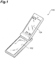
- Fig. 1 is a perspective view of a schematic constitutional view of the cellular phone 100 which is the information processing device of this embodiment.
- the cellular phone 100 comprises the electrostatic pad input acceptance section 102 and the screen display section 104.
- the hardware button input acceptance section 101 is disposed below the electrostatic pad input acceptance section 102.
- the electrostatic pad input acceptance section 102 is formed by an elastic and transparent member and the user is able to perform an input operation with respect to the electrostatic pad input acceptance section 102 and is able to perform an input operation via the elastic electrostatic pad input acceptance section 102 with respect to the hardware button input acceptance section 101 which is disposed below the electrostatic pad input acceptance section 102.
- FIG. 2 is a schematic view of the disposition of the hardware button input acceptance section 101 and the electrostatic pad input acceptance section 102.
- a transparent protective sheet 102a formed by an elastic member is disposed above the electrostatic pad input acceptance section 102.
- the hardware button input acceptance section 101 is disposed below the electrostatic pad input acceptance section 102.
- the protective sheet 102a and the electrostatic pad input acceptance section 102 are constituted by transparent members and the user is therefore able to visually check the characters (numerical characters) which are printed on each key top of the hardware button input acceptance section 101 disposed below the protective sheet 102a and the electrostatic pad input acceptance section 102. Further, as mentioned hereinabove, in a case where the electrostatic pad input acceptance section 102 and protective sheet 102a are constituted by elastic members and the user presses one point of the protective sheet 102a and the electrostatic pad input acceptance section 102, the pressing force is transmitted to the hardware button input acceptance section 101 disposed below the protective sheet 102a and the electrostatic pad input acceptance section 102. The hardware button input acceptance section 101 is then capable of accepting inputs via the electrostatic pad input acceptance section 102.
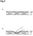
- Fig. 3 is a cross-sectional view in the direction of the arrow III-III in the schematic constitutional view of Fig. 2 .
- the protective sheet 102a, the electrostatic pad input acceptance section 102, and the hardware button input acceptance section 101 are disposed in that order starting from the top.
- the user is able to press one button of the hardware button input acceptance section 101 which is disposed in the lowest layer with his finger by utilizing the elasticity of the protective sheet 102a and the electrostatic pad input acceptance section 102, as shown in (b) of Fig. 3 .
- Fig. 4 is a block diagram showing the constitution of the cellular phone 100 of this embodiment.
- the cellular phone 100 is constituted comprising the hardware button input acceptance section 101, the electrostatic pad input acceptance section 102, an input device control section 103, the screen display section 104, a screen display control section 105, an object detection section 106, a memory 107, the data table 108, and a CPU 109.
- the respective constitutions of the aforementioned parts will be described hereinbelow.
- the hardware button input acceptance section 101 is an operating button which is constituted by hardware.
- the hardware button input acceptance section 101 is constituted by key tops and dome switches which are disposed below the key tops and the hardware button input acceptance section 101 is constituted such that the hardware button input acceptance section 101 is capable of passing an electrical current as a result of contact between an operating contact and a fixed contact, which are formed in the dome switches, when a key top is pressed by the user.
- the electrostatic pad input acceptance section 102 is an input member which detects the position of the user's finger or the like which is touching the pad by using the coordinates X and Y to specify the position of the user's finger.
- the electrostatic pad input acceptance section 102 is able to detect the touched position and, in cases where the user touches the pad by tracing his finger over the pad, is able to detect the track which the user traces.
- the electrostatic pad input acceptance section 102 is able to detect the position of the user's finger even via the protective sheet 102a.
- the input device control section 103 is a part which outputs an input instruction that is accepted by the hardware button input acceptance section 101 or the electrostatic pad input acceptance section 102 to the CPU 109.
- the CPU 109 judges whether input acceptance is placed in an ON state in accordance with setting information which is described in the data table 108. Furthermore, the result of the judgment by the CPU 109 is input to the input device control section 103 and settings are made such that either input acceptance section is shifted to an ON state by the input device control section 103.
- the input device control section 103 performs switching processing on the basis of this set state.
- the screen display section 104 is a part which displays information to the user and is constituted by a display or LED, for example.
- the object detection section 106 is a part which detects a predetermined object and is formed on the screen which has undergone display processing under the control of an application which is running.
- This object detection section 106 is, for example, a part which detects that the pointer operated by means of the electrostatic pad input acceptance section 102 is a character input part in cases where an object representing a character input part is shown.
- the memory 107 is a part which has an area for storing an application program.
- the data table 108 is a part which stores conditions for switching between the hardware button input acceptance section 101 and the electrostatic pad input acceptance section 102 and is a part which associates and stores the name of the application currently running with setting information which represents the ON and OFF states of the electrostatic pad input acceptance section 102, for example.
- Fig. 5 is an explanatory diagram of the data table 108 of this embodiment. As shown in Fig. 5 , the name of the application running and the setting information which indicates the ON and OFF of the electrostatic pad input acceptance section 102 are associated and stored in the data table 108. In the example of Fig.
- settings are such that an ON state is established in order to be able to accept inputs of the electrostatic pad input acceptance section 102 in cases where a full browser is running and settings are such that an OFF state is established in order to be able to accept inputs of the electrostatic pad input acceptance section 102 in cases where a character inputting-based application such as a notebook application is running.
- the CPU 109 is a part which performs overall parts control, from the hardware button input acceptance section 101 to the data table 108.
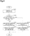
- Fig. 6 is a flowchart showing the operation of the cellular phone 100.
- the application is read from the memory 107 and run by means of a user operation (S101).
- S101 a user operation
- settings are preferably made such that the electrostatic pad input acceptance section 102 is turned OFF and the hardware button input acceptance section 101 is turned ON (is prioritized).
- the data table 108 is referenced by the CPU 109 and it is judged by the CPU 109 whether the application requires inputs of the electrostatic pad input acceptance section 102, that is, whether settings to turn ON the electrostatic pad input acceptance section 102 have been made with respect to the application (S102).
- control to turn ON the inputs for the electrostatic pad input acceptance section 102 is performed with respect to the input device control section 103 (S105).
- the fact that the electrostatic pad input acceptance section 102 is ON is displayed on the screen display section 104 (S106).
- the control to turn ON input acceptance by the hardware button input acceptance section 101 is performed with respect to the input device control section 103 (S103). Furthermore, the fact that the hardware button input acceptance section 101 is ON is displayed on the screen display section 104 (S104). In cases where the hardware button input acceptance section 101 is ON in an initial state, the processing of steps S103 and S104 can be omitted.
- FIG. 7 is a flowchart showing the processing when the hardware button input acceptance section 101 is shifted to an ON state when the application is being operated.
- operation of the electrostatic pad input acceptance section 102 by the user is accepted (S201).
- an operation such as one where the pointer is moved by the user moving his finger over the electrostatic pad, for example, is accepted.
- this character input object is a text box for accepting a character input.
- the detection of a character input object is preferably performed by means of this operation by judging whether a character input object has been detected for a predetermined time.
- the hardware button input acceptance section 101 upon detection of a predetermined object when the electrostatic pad input acceptance section 102 is being operated, the hardware button input acceptance section 101 is automatically controlled to enter an ON state and input acceptance which corresponds to this state can be performed. For example, because the operability of inputting characters by means of the hardware button input acceptance section 101 is considered to be favorable in cases where character inputting is carried out, the hardware button input acceptance section 101 is automatically placed in an ON state.
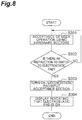
- FIG. 8 is a flowchart showing the processing when the electrostatic pad input acceptance section 102 is shifted to an ON state when the application is being operated.
- the operation of the hardware button input acceptance section 101 by the user is accepted (S301). It is then judged by the CPU 109 whether there is an instruction to switch to the electrostatic pad (S302). Here, in cases where it is judged that there is a switching instruction, the input device control unit 103 is controlled to place the electrostatic pad input acceptance section 102 in an ON state (S303). The fact that the electrostatic pad input acceptance section 102 is in an ON state is then displayed on the screen display section 104 (S304).
- Fig. 9 is an explanatory diagram showing a screen transition when shifting from a menu screen of a mail application to a new mail creation screen.
- a mail menu screen is displayed on the screen display section 104.
- the data table 108 is set so that the electrostatic pad input acceptance section 102 is in an ON state when a mail application is running. The user is then able to make any selection from "1. Inbox” to "7. Mail settings" by operating the pointer on the screen display.
- the screen display section 104 displays a mark 104a which indicates that the electrostatic pad input acceptance section 102 is in an ON state. The user is able to easily grasp whether input acceptance is in an ON state by visually checking this mark.
- the hardware button input acceptance section 101 enters an ON state and the user is able to shift to the new mail creation screen shown in (b) of Fig. 9 by pressing the hardware buttons via the electrostatic pad input acceptance section 102 in this state.
- the mark 104b is displayed, which indicates here that the hardware button input acceptance section 101 is in an ON state.
- Fig. 10 is an explanatory diagram showing a screen transition when shifting from a top menu screen of a search site to a text box input screen.
- the top menu screen of the search site is displayed on the screen display section 104.
- the data table 108 is set so that the electrostatic pad input acceptance section 102 enters an ON state when a mail application is running.
- the user then operates the pointer on the screen display and shifts the pointer onto a text box 104c.
- the object detection section 106 shifts the screen to a character input screen for inputting search characters as shown in (b) of Fig. 10 .
- Marks 104a and 104b are displayed in (a) of Fig. 10 and (b) of Fig. 10 as per (a) of Fig. 9 and (b) of Fig. 9 and the display screen is constituted such that same can be visually checked by the user.
- FIG. 11 is a schematic view of the disposition of the hardware button input acceptance section 101, the electrostatic pad input acceptance section 102, and the screen display section 104, which are in the cellular phone 100 of the modified example of this embodiment.
- the electrostatic pad input acceptance section 102 is disposed under the protective sheet 102a
- the screen display section 104 which is a display or the like is disposed under the electrostatic pad input acceptance section 102
- the hardware button input acceptance section 101 is disposed under the screen display section 104.
- the protective sheet 102a and the electrostatic pad input acceptance section 102 are formed by transparent members and the information displayed by the screen display section 104 can therefore be visually checked by the user.
- the screen display section 104 is constituted by electronic paper, for example.
- the screen display section 104 is a permeable member or a transparent member and the user is therefore able to recognize the buttons of the hardware button input acceptance section 101 which is disposed below the screen display section 104 and is able to perform an input operation with respect to the hardware button input acceptance section 101.
- Fig. 12 shows a cross-sectional view in the direction of the arrow XII-XII of the cellular phone 100 of this modified example.
- the protective sheet 102a, the electrostatic pad input acceptance section 102, the screen display section 104, and the hardware button input acceptance section 101 are disposed in that order.
- the protective sheet 102a, the electrostatic pad input acceptance section 101, and the screen display section 104 bend due to their elasticity and this one button thus comes to be pressed.
- the space where the screen display section 104 is disposed can be omitted, the device can be miniaturized, and the amount of information that can be displayed can be increased even for a device of the same size.
- the CPU 109 is able to judge the application which is to be the user operation target and the input device control section 103 is able to judge and switch between accepting inputs from the electrostatic pad input acceptance section 102 and accepting inputs from the hardware button input acceptance section 101 in accordance with the application thus judged.
- the hardware button input acceptance section 101 and the electrostatic pad input acceptance section 102 are disposed to be stacked, it is possible to provide a user-friendly device which is capable of suitably and automatically switching between the hardware button input acceptance section 101 and the electrostatic pad input acceptance section 102 depending on the usage state thereof, without the user making a manual selection between operating the hardware button input acceptance section 101 and the electrostatic pad input acceptance section 102.
- the object detection section 106 detects that a pointer, which is operated by means of the electrostatic pad input acceptance section 102, is pointing to a predetermined object among objects which are displayed on the operation screen displayed by the screen display section 104 and, in cases where the predetermined object is detected, the CPU 109 is able to switch between placing the electrostatic pad input acceptance section 102 in an OFF state and placing the hardware button input acceptance section 101 in an ON state.
- the input device control section 103 is capable of switching the input from the electrostatic pad input acceptance section 102 to the hardware button input acceptance section 101 depending on the object, whereby a user-friendly device can be provided.
- the screen display section 104 produces a display indicating whether the electrostatic pad input acceptance section 102 or the hardware button input acceptance section 101 is in an ON state, whereby the user is easily able to ascertain whether he may use either the electrostatic pad input acceptance section 102 or the hardware button input acceptance section 101.
- the device constitution of the cellular phone 100 can be reduced by disposing the screen display section 104 stacked between the electrostatic pad input acceptance section 102 and the hardware button input acceptance section 101, which are constituted by transparent members.
Claims (3)
- Eine Informationsverarbeitungsvorrichtung (100), aufweisend:• ein Berührungspanel (102), welches eine Eingabe von einem Nutzer annimmt;• Hardwaretasten (101), welche geschichtet unter dem Berührungspanel (102) angeordnet sind und eine Eingabe von dem Nutzer annehmen;• ein Anzeigemittel (104) zum Anzeigen eines Bedienbildschirms, auf welchem ein Zeiger mittels der von dem Berührungspanel (102) angenommenen Eingabe bedient werden kann;
gekennzeichnet durch• ein Beurteilungsmittel (109) zum Beurteilen einer Anwendung, welche ein Nutzerbetriebsziel darstellt;• ein Umschaltmittel (103) zum Umschalten zwischen einer Eingabeannahme von dem Berührungspanel (102) und einer Eingabeannahme von den Hardwaretasten (101) in Abhängigkeit von der von dem Beurteilungsmittel (109) beurteilten Anwendung;• wobei das Berührungspanel (102) und die Hardwaretasten (101) aus transparenten Elementen gebildet sind, das Anzeigemittel (104) unter dem Berührungspanel (102) angeordnet ist, und die Hardwaretasten (101) unter dem Anzeigemittel (104) angeordnet sind. - Die Informationsverarbeitungsvorrichtung (100) gemäß Anspruch 1, ferner aufweisend:• ein Erfassungsmittel zum Erfassen, dass der Zeiger, welcher mittels des Berührungspanels (102) bedient wird, auf ein vorbestimmtes Objekt von Objekten zeigt, welche auf dem von dem Anzeigemittel (104) angezeigten Bedienbildschirm angezeigt werden, wobei• in Fällen, in denen das vorbestimmte Objekt von dem Erfassungsmittel erfasst wird, das Umschaltmittel (103) das Berührungspanel (102) in einen AUS-Zustand schaltet, in welchem Eingaben von dem Berührungspanel (102) nicht angenommen werden, und die Hardwaretasten (101) in einen AN-Zustand schaltet, in welchem Eingaben von den Hardwaretasten (101) angenommen werden.
- Die Informationsverarbeitungsvorrichtung (100) gemäß Anspruch 1,
wobei das Anzeigemittel (104) eine Anzeige erzeugt, welche angibt, ob das Berührungspanel (102) oder die Hardwaretasten (101) in einem AN-Zustand sind.
Applications Claiming Priority (1)
| Application Number | Priority Date | Filing Date | Title |
|---|---|---|---|
| JP2007323705A JP4871251B2 (ja) | 2007-12-14 | 2007-12-14 | 情報処理装置 |
Publications (2)
| Publication Number | Publication Date |
|---|---|
| EP2071430A1 EP2071430A1 (de) | 2009-06-17 |
| EP2071430B1 true EP2071430B1 (de) | 2018-06-20 |
Family
ID=40427329
Family Applications (1)
| Application Number | Title | Priority Date | Filing Date |
|---|---|---|---|
| EP08171535.1A Expired - Fee Related EP2071430B1 (de) | 2007-12-14 | 2008-12-12 | Informationsverarbeitungsvorrichtung |
Country Status (4)
| Country | Link |
|---|---|
| US (1) | US8508473B2 (de) |
| EP (1) | EP2071430B1 (de) |
| JP (1) | JP4871251B2 (de) |
| CN (1) | CN101458562B (de) |
Families Citing this family (6)
| Publication number | Priority date | Publication date | Assignee | Title |
|---|---|---|---|---|
| CN102236514A (zh) * | 2010-05-07 | 2011-11-09 | 英业达股份有限公司 | 电子装置及其虚拟键盘的切换方法 |
| JP5841714B2 (ja) * | 2010-07-27 | 2016-01-13 | 京セラ株式会社 | 触感呈示装置及び触感呈示装置の制御方法 |
| JP2012027855A (ja) * | 2010-07-27 | 2012-02-09 | Kyocera Corp | 触感呈示装置及び触感呈示装置の制御方法 |
| JP3167103U (ja) * | 2011-01-24 | 2011-04-07 | 株式会社シティ | 装飾シート |
| EP3318050B8 (de) * | 2015-07-03 | 2020-08-05 | Telecalm, Inc. | Telefonsystem für beeinträchtigte personen |
| JP6276329B2 (ja) * | 2016-06-15 | 2018-02-07 | 京セラ株式会社 | 携帯通信端末、設定方法およびプログラム |
Citations (1)
| Publication number | Priority date | Publication date | Assignee | Title |
|---|---|---|---|---|
| GB2402105A (en) * | 2003-05-30 | 2004-12-01 | Therefore Ltd | Data input method for a computing device |
Family Cites Families (13)
| Publication number | Priority date | Publication date | Assignee | Title |
|---|---|---|---|---|
| JP4939682B2 (ja) * | 1999-04-27 | 2012-05-30 | エーユー オプトロニクス コーポレイション | 表示装置 |
| WO2001071478A2 (en) * | 2000-03-22 | 2001-09-27 | Sony Electronics Inc | Data entry user interface |
| JP3943876B2 (ja) | 2000-08-11 | 2007-07-11 | アルプス電気株式会社 | 入力装置及びこれを備えた電子機器 |
| GB2367530B (en) * | 2000-10-03 | 2003-07-23 | Nokia Mobile Phones Ltd | User interface device |
| JP4057253B2 (ja) * | 2001-05-29 | 2008-03-05 | アルプス電気株式会社 | 入力装置及び電子機器 |
| CN1559029A (zh) * | 2001-11-16 | 2004-12-29 | 米厄里戈公司 | 扩充式键盘 |
| CN2574121Y (zh) | 2002-09-17 | 2003-09-17 | 鸿富锦精密工业(深圳)有限公司 | 便携式电子装置 |
| US7010333B2 (en) * | 2003-02-19 | 2006-03-07 | Sony Ericsson Mobile Communications Ab | Radiotelephone terminal with dual-sided keypad apparatus |
| JP2006042123A (ja) | 2004-07-29 | 2006-02-09 | Mitsumi Electric Co Ltd | 携帯電話 |
| TWI340884B (en) | 2005-08-10 | 2011-04-21 | Asustek Comp Inc | Electric device with trace identification mode and keypad identification mode |
| JP2007052643A (ja) * | 2005-08-18 | 2007-03-01 | Canon Inc | 表示装置 |
| KR100791378B1 (ko) * | 2005-12-29 | 2008-01-07 | 삼성전자주식회사 | 다양한 입력 모드를 지원하는 사용자 명령 입력 장치 및이를 이용한 기기 |
| US20070152983A1 (en) * | 2005-12-30 | 2007-07-05 | Apple Computer, Inc. | Touch pad with symbols based on mode |
-
2007
- 2007-12-14 JP JP2007323705A patent/JP4871251B2/ja active Active
-
2008
- 2008-12-08 US US12/329,877 patent/US8508473B2/en not_active Expired - Fee Related
- 2008-12-12 EP EP08171535.1A patent/EP2071430B1/de not_active Expired - Fee Related
- 2008-12-12 CN CN2008101869926A patent/CN101458562B/zh not_active Expired - Fee Related
Patent Citations (1)
| Publication number | Priority date | Publication date | Assignee | Title |
|---|---|---|---|---|
| GB2402105A (en) * | 2003-05-30 | 2004-12-01 | Therefore Ltd | Data input method for a computing device |
Also Published As
| Publication number | Publication date |
|---|---|
| EP2071430A1 (de) | 2009-06-17 |
| CN101458562A (zh) | 2009-06-17 |
| JP4871251B2 (ja) | 2012-02-08 |
| CN101458562B (zh) | 2012-10-24 |
| JP2009146212A (ja) | 2009-07-02 |
| US20090153489A1 (en) | 2009-06-18 |
| US8508473B2 (en) | 2013-08-13 |
Similar Documents
| Publication | Publication Date | Title |
|---|---|---|
| US20200225835A1 (en) | Portable terminal device and display control method | |
| KR101372753B1 (ko) | 터치스크린을 구비한 단말기에서의 입력 방법 및 장치 | |
| EP2423780B1 (de) | Mobiles Informationsendgerät | |
| US8351992B2 (en) | Portable electronic apparatus, and a method of controlling a user interface thereof | |
| KR100617821B1 (ko) | 사용자 인터페이스 장치 및 방법 | |
| JP4787087B2 (ja) | 位置検出装置及び情報処理装置 | |
| EP2071430B1 (de) | Informationsverarbeitungsvorrichtung | |
| EP2211255A1 (de) | Eingabevorrichtung für ein mobiles elektronisches gerät und mobiles elektronisches gerät | |
| EP3190482B1 (de) | Elektronische vorrichtung, zeicheneingabemodul und verfahren zur auswahl von zeichen daraus | |
| CN101692195A (zh) | 用于触摸屏上的控制菜单的显示以及控制方法 | |
| US20110316811A1 (en) | Input device of portable electronic apparatus, control method of input device, and program | |
| GB2445178A (en) | A single touchpad to enable cursor control and keypad emulation on a mobile electronic device | |
| EP2818984B1 (de) | Eingabevorrichtung für berührungsbildschirm und steuerverfahren dafür | |
| JP4521335B2 (ja) | 携帯端末 | |
| JP2012073698A (ja) | 携帯端末装置 | |
| JP4972183B2 (ja) | 携帯端末 |
Legal Events
| Date | Code | Title | Description |
|---|---|---|---|
| PUAI | Public reference made under article 153(3) epc to a published international application that has entered the european phase |
Free format text: ORIGINAL CODE: 0009012 |
|
| 17P | Request for examination filed |
Effective date: 20081212 |
|
| AK | Designated contracting states |
Kind code of ref document: A1 Designated state(s): AT BE BG CH CY CZ DE DK EE ES FI FR GB GR HR HU IE IS IT LI LT LU LV MC MT NL NO PL PT RO SE SI SK TR |
|
| AX | Request for extension of the european patent |
Extension state: AL BA MK RS |
|
| AKX | Designation fees paid |
Designated state(s): DE GB |
|
| 17Q | First examination report despatched |
Effective date: 20100621 |
|
| REG | Reference to a national code |
Ref country code: DE Ref legal event code: R079 Ref document number: 602008055674 Country of ref document: DE Free format text: PREVIOUS MAIN CLASS: G06F0003020000 Ipc: G06F0003048800 |
|
| GRAP | Despatch of communication of intention to grant a patent |
Free format text: ORIGINAL CODE: EPIDOSNIGR1 |
|
| RIC1 | Information provided on ipc code assigned before grant |
Ipc: G06F 3/038 20130101ALI20180115BHEP Ipc: G06F 3/0488 20130101AFI20180115BHEP Ipc: G06F 3/023 20060101ALI20180115BHEP Ipc: H04M 1/23 20060101ALI20180115BHEP Ipc: G06F 3/0354 20130101ALI20180115BHEP |
|
| INTG | Intention to grant announced |
Effective date: 20180214 |
|
| GRAS | Grant fee paid |
Free format text: ORIGINAL CODE: EPIDOSNIGR3 |
|
| GRAA | (expected) grant |
Free format text: ORIGINAL CODE: 0009210 |
|
| AK | Designated contracting states |
Kind code of ref document: B1 Designated state(s): DE GB |
|
| REG | Reference to a national code |
Ref country code: GB Ref legal event code: FG4D |
|
| REG | Reference to a national code |
Ref country code: DE Ref legal event code: R096 Ref document number: 602008055674 Country of ref document: DE |
|
| RIC2 | Information provided on ipc code assigned after grant |
Ipc: G06F 3/023 20060101ALI20180115BHEP Ipc: G06F 3/038 20130101ALI20180115BHEP Ipc: H04M 1/23 20060101ALI20180115BHEP Ipc: G06F 3/0354 20130101ALI20180115BHEP Ipc: G06F 3/0488 20130101AFI20180115BHEP |
|
| REG | Reference to a national code |
Ref country code: DE Ref legal event code: R097 Ref document number: 602008055674 Country of ref document: DE |
|
| PLBE | No opposition filed within time limit |
Free format text: ORIGINAL CODE: 0009261 |
|
| STAA | Information on the status of an ep patent application or granted ep patent |
Free format text: STATUS: NO OPPOSITION FILED WITHIN TIME LIMIT |
|
| 26N | No opposition filed |
Effective date: 20190321 |
|
| PGFP | Annual fee paid to national office [announced via postgrant information from national office to epo] |
Ref country code: DE Payment date: 20191126 Year of fee payment: 12 |
|
| PGFP | Annual fee paid to national office [announced via postgrant information from national office to epo] |
Ref country code: GB Payment date: 20191213 Year of fee payment: 12 |
|
| REG | Reference to a national code |
Ref country code: DE Ref legal event code: R119 Ref document number: 602008055674 Country of ref document: DE |
|
| GBPC | Gb: european patent ceased through non-payment of renewal fee |
Effective date: 20201212 |
|
| PG25 | Lapsed in a contracting state [announced via postgrant information from national office to epo] |
Ref country code: GB Free format text: LAPSE BECAUSE OF NON-PAYMENT OF DUE FEES Effective date: 20201212 Ref country code: DE Free format text: LAPSE BECAUSE OF NON-PAYMENT OF DUE FEES Effective date: 20210701 |