EP2067217B1 - Electrically tunable terahertz laser oscillation device - Google Patents
Electrically tunable terahertz laser oscillation device Download PDFInfo
- Publication number
- EP2067217B1 EP2067217B1 EP07851121.9A EP07851121A EP2067217B1 EP 2067217 B1 EP2067217 B1 EP 2067217B1 EP 07851121 A EP07851121 A EP 07851121A EP 2067217 B1 EP2067217 B1 EP 2067217B1
- Authority
- EP
- European Patent Office
- Prior art keywords
- electrode
- gain medium
- clad
- electromagnetic wave
- oscillation device
- Prior art date
- Legal status (The legal status is an assumption and is not a legal conclusion. Google has not performed a legal analysis and makes no representation as to the accuracy of the status listed.)
- Not-in-force
Links
- 230000010355 oscillation Effects 0.000 title claims description 78
- 239000004065 semiconductor Substances 0.000 claims description 23
- 230000005641 tunneling Effects 0.000 claims description 21
- 239000000969 carrier Substances 0.000 claims description 7
- 238000000926 separation method Methods 0.000 claims description 5
- 238000005086 pumping Methods 0.000 claims description 3
- 230000005684 electric field Effects 0.000 description 40
- 238000000034 method Methods 0.000 description 26
- 239000000758 substrate Substances 0.000 description 26
- 230000008859 change Effects 0.000 description 22
- 238000010586 diagram Methods 0.000 description 18
- 229910000530 Gallium indium arsenide Inorganic materials 0.000 description 14
- 238000009826 distribution Methods 0.000 description 11
- 238000004364 calculation method Methods 0.000 description 10
- 239000010408 film Substances 0.000 description 9
- 125000006850 spacer group Chemical group 0.000 description 8
- 229910000577 Silicon-germanium Inorganic materials 0.000 description 7
- 239000000463 material Substances 0.000 description 7
- 230000003287 optical effect Effects 0.000 description 7
- 238000012546 transfer Methods 0.000 description 7
- 230000004888 barrier function Effects 0.000 description 6
- 230000007704 transition Effects 0.000 description 6
- 239000003989 dielectric material Substances 0.000 description 5
- 230000006870 function Effects 0.000 description 5
- 239000002184 metal Substances 0.000 description 5
- 229910052751 metal Inorganic materials 0.000 description 5
- 230000008569 process Effects 0.000 description 5
- 229910000673 Indium arsenide Inorganic materials 0.000 description 4
- 230000008901 benefit Effects 0.000 description 4
- 239000002019 doping agent Substances 0.000 description 4
- 238000005530 etching Methods 0.000 description 4
- RPQDHPTXJYYUPQ-UHFFFAOYSA-N indium arsenide Chemical compound [In]#[As] RPQDHPTXJYYUPQ-UHFFFAOYSA-N 0.000 description 4
- 230000003071 parasitic effect Effects 0.000 description 4
- 239000010409 thin film Substances 0.000 description 4
- 229910001218 Gallium arsenide Inorganic materials 0.000 description 3
- BJQHLKABXJIVAM-UHFFFAOYSA-N bis(2-ethylhexyl) phthalate Chemical compound CCCCC(CC)COC(=O)C1=CC=CC=C1C(=O)OCC(CC)CCCC BJQHLKABXJIVAM-UHFFFAOYSA-N 0.000 description 3
- 230000008878 coupling Effects 0.000 description 3
- 238000010168 coupling process Methods 0.000 description 3
- 238000005859 coupling reaction Methods 0.000 description 3
- 238000005516 engineering process Methods 0.000 description 3
- 230000001965 increasing effect Effects 0.000 description 3
- 238000002347 injection Methods 0.000 description 3
- 239000007924 injection Substances 0.000 description 3
- 238000003475 lamination Methods 0.000 description 3
- 230000004048 modification Effects 0.000 description 3
- 238000012986 modification Methods 0.000 description 3
- VEXZGXHMUGYJMC-UHFFFAOYSA-N Hydrochloric acid Chemical compound Cl VEXZGXHMUGYJMC-UHFFFAOYSA-N 0.000 description 2
- 230000015572 biosynthetic process Effects 0.000 description 2
- 238000005253 cladding Methods 0.000 description 2
- 230000003247 decreasing effect Effects 0.000 description 2
- 238000004519 manufacturing process Methods 0.000 description 2
- 238000001451 molecular beam epitaxy Methods 0.000 description 2
- 230000009466 transformation Effects 0.000 description 2
- 238000001039 wet etching Methods 0.000 description 2
- 229910017115 AlSb Inorganic materials 0.000 description 1
- -1 Si) Substances 0.000 description 1
- 230000005699 Stark effect Effects 0.000 description 1
- 238000010521 absorption reaction Methods 0.000 description 1
- 229910052782 aluminium Inorganic materials 0.000 description 1
- 238000004458 analytical method Methods 0.000 description 1
- 230000005540 biological transmission Effects 0.000 description 1
- 239000011248 coating agent Substances 0.000 description 1
- 238000000576 coating method Methods 0.000 description 1
- 238000004891 communication Methods 0.000 description 1
- 239000004020 conductor Substances 0.000 description 1
- 229910052802 copper Inorganic materials 0.000 description 1
- 230000001419 dependent effect Effects 0.000 description 1
- 238000011161 development Methods 0.000 description 1
- 230000018109 developmental process Effects 0.000 description 1
- 238000001312 dry etching Methods 0.000 description 1
- 230000002708 enhancing effect Effects 0.000 description 1
- 239000003574 free electron Substances 0.000 description 1
- 229910052737 gold Inorganic materials 0.000 description 1
- 238000007689 inspection Methods 0.000 description 1
- 230000007246 mechanism Effects 0.000 description 1
- 238000000206 photolithography Methods 0.000 description 1
- 229920002120 photoresistant polymer Polymers 0.000 description 1
- 239000011295 pitch Substances 0.000 description 1
- 230000010287 polarization Effects 0.000 description 1
- 230000000644 propagated effect Effects 0.000 description 1
- 230000011218 segmentation Effects 0.000 description 1
- 238000005204 segregation Methods 0.000 description 1
- 229910052709 silver Inorganic materials 0.000 description 1
- 229910000679 solder Inorganic materials 0.000 description 1
- 238000001228 spectrum Methods 0.000 description 1
- 238000010408 sweeping Methods 0.000 description 1
Images


Classifications
-
- H—ELECTRICITY
- H01—ELECTRIC ELEMENTS
- H01S—DEVICES USING THE PROCESS OF LIGHT AMPLIFICATION BY STIMULATED EMISSION OF RADIATION [LASER] TO AMPLIFY OR GENERATE LIGHT; DEVICES USING STIMULATED EMISSION OF ELECTROMAGNETIC RADIATION IN WAVE RANGES OTHER THAN OPTICAL
- H01S1/00—Masers, i.e. devices using stimulated emission of electromagnetic radiation in the microwave range
- H01S1/02—Masers, i.e. devices using stimulated emission of electromagnetic radiation in the microwave range solid
-
- B—PERFORMING OPERATIONS; TRANSPORTING
- B82—NANOTECHNOLOGY
- B82Y—SPECIFIC USES OR APPLICATIONS OF NANOSTRUCTURES; MEASUREMENT OR ANALYSIS OF NANOSTRUCTURES; MANUFACTURE OR TREATMENT OF NANOSTRUCTURES
- B82Y20/00—Nanooptics, e.g. quantum optics or photonic crystals
-
- H—ELECTRICITY
- H01—ELECTRIC ELEMENTS
- H01S—DEVICES USING THE PROCESS OF LIGHT AMPLIFICATION BY STIMULATED EMISSION OF RADIATION [LASER] TO AMPLIFY OR GENERATE LIGHT; DEVICES USING STIMULATED EMISSION OF ELECTROMAGNETIC RADIATION IN WAVE RANGES OTHER THAN OPTICAL
- H01S5/00—Semiconductor lasers
- H01S5/06—Arrangements for controlling the laser output parameters, e.g. by operating on the active medium
- H01S5/062—Arrangements for controlling the laser output parameters, e.g. by operating on the active medium by varying the potential of the electrodes
- H01S5/0625—Arrangements for controlling the laser output parameters, e.g. by operating on the active medium by varying the potential of the electrodes in multi-section lasers
- H01S5/06255—Controlling the frequency of the radiation
-
- H—ELECTRICITY
- H01—ELECTRIC ELEMENTS
- H01S—DEVICES USING THE PROCESS OF LIGHT AMPLIFICATION BY STIMULATED EMISSION OF RADIATION [LASER] TO AMPLIFY OR GENERATE LIGHT; DEVICES USING STIMULATED EMISSION OF ELECTROMAGNETIC RADIATION IN WAVE RANGES OTHER THAN OPTICAL
- H01S5/00—Semiconductor lasers
- H01S5/30—Structure or shape of the active region; Materials used for the active region
- H01S5/34—Structure or shape of the active region; Materials used for the active region comprising quantum well or superlattice structures, e.g. single quantum well [SQW] lasers, multiple quantum well [MQW] lasers or graded index separate confinement heterostructure [GRINSCH] lasers
- H01S5/3401—Structure or shape of the active region; Materials used for the active region comprising quantum well or superlattice structures, e.g. single quantum well [SQW] lasers, multiple quantum well [MQW] lasers or graded index separate confinement heterostructure [GRINSCH] lasers having no PN junction, e.g. unipolar lasers, intersubband lasers, quantum cascade lasers
- H01S5/3402—Structure or shape of the active region; Materials used for the active region comprising quantum well or superlattice structures, e.g. single quantum well [SQW] lasers, multiple quantum well [MQW] lasers or graded index separate confinement heterostructure [GRINSCH] lasers having no PN junction, e.g. unipolar lasers, intersubband lasers, quantum cascade lasers intersubband lasers, e.g. transitions within the conduction or valence bands
-
- H—ELECTRICITY
- H01—ELECTRIC ELEMENTS
- H01S—DEVICES USING THE PROCESS OF LIGHT AMPLIFICATION BY STIMULATED EMISSION OF RADIATION [LASER] TO AMPLIFY OR GENERATE LIGHT; DEVICES USING STIMULATED EMISSION OF ELECTROMAGNETIC RADIATION IN WAVE RANGES OTHER THAN OPTICAL
- H01S5/00—Semiconductor lasers
- H01S5/06—Arrangements for controlling the laser output parameters, e.g. by operating on the active medium
- H01S5/062—Arrangements for controlling the laser output parameters, e.g. by operating on the active medium by varying the potential of the electrodes
- H01S5/0625—Arrangements for controlling the laser output parameters, e.g. by operating on the active medium by varying the potential of the electrodes in multi-section lasers
- H01S5/06255—Controlling the frequency of the radiation
- H01S5/06256—Controlling the frequency of the radiation with DBR-structure
-
- H—ELECTRICITY
- H01—ELECTRIC ELEMENTS
- H01S—DEVICES USING THE PROCESS OF LIGHT AMPLIFICATION BY STIMULATED EMISSION OF RADIATION [LASER] TO AMPLIFY OR GENERATE LIGHT; DEVICES USING STIMULATED EMISSION OF ELECTROMAGNETIC RADIATION IN WAVE RANGES OTHER THAN OPTICAL
- H01S5/00—Semiconductor lasers
- H01S5/20—Structure or shape of the semiconductor body to guide the optical wave ; Confining structures perpendicular to the optical axis, e.g. index or gain guiding, stripe geometry, broad area lasers, gain tailoring, transverse or lateral reflectors, special cladding structures, MQW barrier reflection layers
- H01S5/22—Structure or shape of the semiconductor body to guide the optical wave ; Confining structures perpendicular to the optical axis, e.g. index or gain guiding, stripe geometry, broad area lasers, gain tailoring, transverse or lateral reflectors, special cladding structures, MQW barrier reflection layers having a ridge or stripe structure
- H01S5/2205—Structure or shape of the semiconductor body to guide the optical wave ; Confining structures perpendicular to the optical axis, e.g. index or gain guiding, stripe geometry, broad area lasers, gain tailoring, transverse or lateral reflectors, special cladding structures, MQW barrier reflection layers having a ridge or stripe structure comprising special burying or current confinement layers
- H01S5/2213—Structure or shape of the semiconductor body to guide the optical wave ; Confining structures perpendicular to the optical axis, e.g. index or gain guiding, stripe geometry, broad area lasers, gain tailoring, transverse or lateral reflectors, special cladding structures, MQW barrier reflection layers having a ridge or stripe structure comprising special burying or current confinement layers based on polyimide or resin
-
- H—ELECTRICITY
- H01—ELECTRIC ELEMENTS
- H01S—DEVICES USING THE PROCESS OF LIGHT AMPLIFICATION BY STIMULATED EMISSION OF RADIATION [LASER] TO AMPLIFY OR GENERATE LIGHT; DEVICES USING STIMULATED EMISSION OF ELECTROMAGNETIC RADIATION IN WAVE RANGES OTHER THAN OPTICAL
- H01S5/00—Semiconductor lasers
- H01S5/20—Structure or shape of the semiconductor body to guide the optical wave ; Confining structures perpendicular to the optical axis, e.g. index or gain guiding, stripe geometry, broad area lasers, gain tailoring, transverse or lateral reflectors, special cladding structures, MQW barrier reflection layers
- H01S5/22—Structure or shape of the semiconductor body to guide the optical wave ; Confining structures perpendicular to the optical axis, e.g. index or gain guiding, stripe geometry, broad area lasers, gain tailoring, transverse or lateral reflectors, special cladding structures, MQW barrier reflection layers having a ridge or stripe structure
- H01S5/227—Buried mesa structure ; Striped active layer
-
- H—ELECTRICITY
- H01—ELECTRIC ELEMENTS
- H01S—DEVICES USING THE PROCESS OF LIGHT AMPLIFICATION BY STIMULATED EMISSION OF RADIATION [LASER] TO AMPLIFY OR GENERATE LIGHT; DEVICES USING STIMULATED EMISSION OF ELECTROMAGNETIC RADIATION IN WAVE RANGES OTHER THAN OPTICAL
- H01S5/00—Semiconductor lasers
- H01S5/30—Structure or shape of the active region; Materials used for the active region
- H01S5/3027—IV compounds
- H01S5/3031—Si
-
- H—ELECTRICITY
- H01—ELECTRIC ELEMENTS
- H01S—DEVICES USING THE PROCESS OF LIGHT AMPLIFICATION BY STIMULATED EMISSION OF RADIATION [LASER] TO AMPLIFY OR GENERATE LIGHT; DEVICES USING STIMULATED EMISSION OF ELECTROMAGNETIC RADIATION IN WAVE RANGES OTHER THAN OPTICAL
- H01S5/00—Semiconductor lasers
- H01S5/30—Structure or shape of the active region; Materials used for the active region
- H01S5/34—Structure or shape of the active region; Materials used for the active region comprising quantum well or superlattice structures, e.g. single quantum well [SQW] lasers, multiple quantum well [MQW] lasers or graded index separate confinement heterostructure [GRINSCH] lasers
- H01S5/3422—Structure or shape of the active region; Materials used for the active region comprising quantum well or superlattice structures, e.g. single quantum well [SQW] lasers, multiple quantum well [MQW] lasers or graded index separate confinement heterostructure [GRINSCH] lasers comprising type-II quantum wells or superlattices
Definitions
- the present invention relates to an oscillation device including a gain medium sandwiched between negative permittivity media of which real part of permittivity with respect to an electromagnetic wave is negative.
- the present invention relates to a current injection type oscillation device including a waveguide through which surface plasmon with an electromagnetic wave having a frequency within a frequency region from 30 GHz to 30 THz (called millimeter wave and terahertz wave, particularly a region near 30 GHz and a region near 30 THz are respectively called millimeter wave band and terahertz band in this specification) is propagated, and serving to change the depletion region by applying an electric field through electric field control means to allow oscillation wavelength to be variable.
- millimeter wave and terahertz wave particularly a region near 30 GHz and a region near 30 THz are respectively called millimeter wave band and terahertz band in this specification
- a new type of semiconductor laser called quantum cascade laser which operates based on transition of carriers between energy levels of carrier within a single energy band such as conduction band or valence band (transition between subbands).
- Oscillation wavelength of a quantum cascade laser depends on level distance between two energy levels with respect to optical transition. Accordingly, oscillation wavelength can be selected over a broad spectrum region (from mid-infrared region to terahertz region). Initially, it was verified that such a laser can be realized by a configuration in which an oscillation wavelength is selected to be equal to 4.2 ⁇ m of the mid-infrared region. In recent years, due to an increasing demand for electromagnetic resource of terahertz region useful for biosensing, longer wavelength lasers having an oscillation wavelength on the longer wavelength side relative to the mid-infrared region has been performed.
- Such a longer wavelength laser includes, along with a configuration of a gain medium having gain in that frequency region, a structure called surface plasmon waveguide capable of performing tight light confinement into the gain medium.
- a longer wavelength laser differs from a conventional semiconductor laser which performs light confinement by using a dielectric clad structure.
- As such a longer wavelength laser there is proposed a configuration using as clad a negative permittivity medium of which real part of permittivity is negative (see Japanese Patent Application Laid-Open No. 2000-138420 ).
- guided by the clad is an electromagnetic wave called surface plasmon to which polarization oscillation of charged carriers within the negative permittivity medium contributes. Since no diffraction limit exists for such surface plasmon, a substantial part of mode intensity can be confined within the gain medium.
- WO 2006/104233 A discloses a frequency tunable oscillator having less gradation of oscillation characteristics due to a parasitic component or the like without mounting therein a lumped constant element such as a variable capacitance element.
- the oscillation frequency can be varied through an external modification by a modification means.
- US 2005/058166 A1 discloses a double-sided metal waveguide that can be utilized in a terahertz laser or amplifier operating in a range of about 1 THz to about 10 THz for mode confinement.
- US 2005/276298 A1 discloses a unipolar semiconductor laser in which an active region is sandwiched in a guiding structure between an upper and lower cladding layer, wherein the lower cladding layer is situated on a semiconductor substrate.
- the configuration using temperature adjustment for allowing oscillation wavelength to be variable in the known long wavelength laser has problems in connection with two points as described below. Namely, the width from the upper limit to the lower limit where oscillation wavelengths are rendered to be variable (wavelength variable width) is relatively narrow, and a rate for sweeping oscillation wavelength (wavelength sweep rate) is relatively low. Therefore, also in long wavelength lasers, a technique for allowing the oscillation wavelength to be variable is required, except for the technique of temperature adjustment, which can solve these problems.
- a scheme is employed to change, at a relatively high rate, the depletion region at the boundary part between the gain medium and the negative permittivity medium to thereby change oscillation wavelength. Accordingly, if a relatively thin gain medium is used (this can be performed as described later), the size of the depletion region can be adjusted by a relatively large ratio with respect to the region of the gain medium. Thus, there can be realized an oscillation device with a long oscillation wavelength, which is broader in wavelength variable width and is higher in wavelength sweep rate, as compared to the related art.
- the oscillation device of the present invention can be effectively applied particularly in the field of millimeter wave and terahertz wave, e.g., to spectrum inspection and identification of material based thereon used in biosensing, as well as high speed information communication.
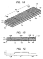
- FIGS. 1A and 1B illustrate the configuration of an exemplary embodiment of an oscillation device to which the present invention is applied.
- negative permittivity media 101 and 102 are materials having negative real part of permittivity in a frequency region of an electromagnetic wave to be oscillated.
- the negative permittivity medium is formed of, e.g., carrier-doped semiconductor (e.g., InAs, InP, GaAs, Si), metal (e.g., Ag, Au, Cu, Al), or these plural materials (metal and carrier-doped semiconductor). Since the negative permittivity medium is also conductive material in the typical case, transparent conductive film (ITO) may be selected.
- ITO transparent conductive film
- a gain medium 103 is sandwiched between the negative permittivity media 101, 102 at upper and lower parts thereof.
- a gain medium is a material such that when pumping energy is injected by energy injection means, a gain is generated.
- the gain medium 103 is a material such that when carrier is injected, gain is generated.
- a high concentration carrier doped semiconductor can be utilized as electrical contacts 111, 112 as occasion demands.
- the high concentration refers to a carrier concentration such that at least real part of permittivity becomes negative.
- electrodes 121 and 122 (122A, 122B).
- the negative permittivity media 101, 102, and electrical contacts 111, 112 function as a clad serving as a geometrical optical reflection plane surface with respect to the millimeter wave and terahertz wave.
- depletion region may take place in a circumstance as described below at boundary parts between the gain medium 103 and negative permittivity media 101, 102. It is to be noted that in the case where the electrical contacts 111, 112 are provided as illustrated in FIGS. 1A, 1B and 1C , the above-mentioned boundary part refers to the boundary between each electrical contact and the gain medium 103.
- the depletion region takes place, the case where electrodes are provided in such a manner that the gain medium 103 is sandwiched therebetween so that an electric field is applied from the electrodes is the typical example thereof.
- the depletion region is a region where carrier concentration is temporarily lowered, and does not temporarily function as a clad with respect to the millimeter wave and terahertz wave which are guided.
- the low concentration refers to a carrier concentration such that the real part of permittivity becomes positive.
- the geometrical reflection plane surface is withdrawn by the depletion region so that the region of the clad is withdrawn.
- the distribution of the guided mode would be enlarged.
- the region of the clad is changed (withdrawn or advanced) by change of the depletion region.
- the distribution of guided mode is increased or decreased (enlarged or contracted).
- the present invention positively uses a phenomenon such that the boundary (serving as geometrical optical reflection plane surface) between the part of the negative real part of permittivity and the part of the positive real part of permittivity in the clad is withdrawn or advanced with respect to the gain medium 103. Further, in order to generate, annihilate or change the depletion region where such a phenomenon takes place, control of an electric field applied to the gain medium forming the waveguide and the part of the clad (negative permittivity medium and electrical contact) is required. Accordingly, change of the equivalent refractive index in the present invention has a mechanism entirely different from change of the equivalent refractive index that the guided mode senses, which is based on current or voltage control known in the wavelength variable optical semiconductor laser, in connection with the following points.
- the present invention differs from the related art in that the negative permittivity medium is used as a clad; that surface plasmon waveguide defined on the geometrical optical reflection plane surface is used; and that the distribution of guided mode is increased or decreased by movement on the reflection plane surface resulting from change of the depletion region to increase or decrease the equivalent refractive index to thereby change resonant wavelength.
- gain medium 103 e.g., a resonant tunneling diode may be used.
- semiconductor multilayer structure including several hundred to several thousand layers used in quantum cascade laser.
- a method for performing electric field control of the depletion region there is a method in which a pair of electrodes applying a drive electric field for injecting carriers into the gain medium 103 are disposed, and a pair of electrodes between which the gain medium 103 is sandwiched are disposed separately therefrom in such a manner to permit electric field control of the depletion region.
- a ground electrode common thereto may be used as ground electrodes in two sets of electrode pairs.
- the electrode 122 is divided into a drive electrode (first electrode) 122A and control electrodes (third electrode) 122B along the propagation direction in the surface plasmon waveguide of an electromagnetic wave to be oscillated, and the electrode 121 is used as a ground electrode (second electrode) to thereby realize the above-mentioned electric field control method.
- the present invention is not limited to such an implementation, there may be provided plural sets of drive electrode pair serving as means for injecting pumping energy, or plural sets of electrode pair serving as electric field application means for performing electric field control of the depletion area.
- the drive electrode 122A injects carries into the gain medium 103 immediately therebelow, and the control electrode 122B performs electric field control of clad of surface plasmon waveguide immediately therebelow. It is sufficient that respective electrodes are connected to external electric field control means (not shown) to respectively perform drive and control. It is to be noted that, in order to facilitate to apply independent electric potential to the electrodes 122A and 122B, i.e., in order to reduce current flowing from the electrode 122A to the electrode 122B via the negative permittivity medium 102, an electrode separation region 123 may be provided at the electrodes 122A and 122B. By the above-mentioned configuration, electric field control of the depletion region can be performed independently of drive.
- control electrodes 122B are provided on both sides of drive electrode in FIGS. 1A and 1B , it is not necessarily required to provide such electrodes on both sides.
- FIG. 1B illustrates an oscillation device cross sectional configuration for indicating a cavity structure.
- FIG. 1C illustrates the state of the distribution of the equivalent refractive index that the guided mode senses.
- the cavity structure is simply formed by end faces 104, 105.
- the surface plasmon guided by clads (negative permittivity media 101, 102 and electrical contacts 111, 112) oscillates by Fabry-Perot etalon formed by these end faces 104, 105 so that oscillation is produced.
- An electric field applied by the control electrode 122B changes n B to change an oscillation wavelength ⁇ as indicated by the formula (1), or to contribute to such a mode hopping to change m.
- wavelength variable width depends upon change of n B .
- ⁇ / ⁇ ⁇ ⁇ n B ⁇ L B / n B ⁇ L A + n B ⁇ L B
- the wavelength variable width ⁇ l/l is proportional to change quantity ⁇ n B of equivalent refractive index that the guided mode senses.
- ⁇ n B equivalent refractive index
- the wavelength variable width is equal to 0.5 ⁇ ⁇ B /n B . Namely, this indicates that change rate ⁇ n B /n B of equivalent refractive index determines wavelength variable width ⁇ / ⁇ rather than change quantity ⁇ n B of equivalent refractive index.
- the present invention it is desired for broadly selecting the wavelength variable width that the change rate of equivalent refractive index that the guided mode senses is relatively large.
- the present invention since there is utilized the phenomenon that a clad is withdrawn by a depletion region produced to broaden the distribution of guided mode, it is sufficient to employ the configuration in which a spread quantity is caused to be an equivalent quantity with respect to the primary guided mode distribution.
- employment of a method of selecting the gain medium 103 having a thickness of the same order of the thickness of the depletion region, or thickness equal to the above or less is simple. This is because there is upper limit in an electric field which can be applied, and the thickness of a depletion region produced indicates the upper limit of the submicron order. Accordingly, it is desirable to select the gain medium 103 having a thickness thinner than that thickness.
- RTD Resonant Tunneling Diode
- RVD Resonant Inter-band Tunneling Diode
- RITD Resonant Inter-band Tunneling Diode
- the RTD uses multiple quantum well including quantum well and tunnelable barrier within conduction band or valence band.
- the RTD in any case is a tunneling diode of the structure to perform inter-subband transition of carriers.
- the RITD is a tunneling diode using tunnelable pn junction or Type II hetero-junction, and having a structure in which carriers perform interband transition.
- This tunneling diode is also called Esaki diode. Since both tunneling diodes are based on tunneling of carriers, it can be said that the thickness of the gain medium 103 can be thinner than the thickness of a depletion region which can be produced.
- the thickness of the gain medium 103 is, e.g., 10 nm.
- the thickness of a depletion region produced at the boundary part between the gain medium 103 and the electrical contacts 111, 112 is, e.g., about 10 nm.
- spread in upper and lower directions (lamination direction) of guided mode is primarily 10 nm.
- both thicknesses are added so that the total thickness becomes equal to 20 nm.
- the thickness of the gain medium 103 is, e.g., 1 nm.
- the thickness of a depletion region produced at the boundary part between the gain medium 103 and the electrical contacts 111, 112 is, e.g., about 1 nm.
- spread in upper and lower directions of the guided mode distribution is primarily 1 nm.
- both thicknesses are added so that the total thickness becomes equal to 2 nm. Therefore, in both cases, there is employed a configuration in which spread becomes equal to an equivalent quantity with respect to the primary guided mode. For this reason, the change rate of equivalent refractive index is relatively large. This is desirable.
- this tunneling diode is a unipolar high speed device in which delay time of carrier is relatively small, high speed operation of, e.g., nano sec. order can be expected as wavelength sweep rate. Namely, as compared to relative low speed heat conduction, or temperature adjustment in which high speed operation is difficult because of relatively large specific heat, the operation speed is high.
- parasitic RF oscillation is oscillation based on RC time constant.
- time constant by an RC resonant circuit from the gain medium 103 up to external electric field application means (not shown) via the electrodes 121, 122 is also a cause of parasitic RF oscillation. Therefore, there may be added a configuration to deliver an electric field between the electrodes 121, 122 through bias T, or a configuration to separately insert a resistor between the electrodes 121, 122.
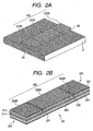
- FIGS. 2A and 2B illustrate a first example of an oscillation device to which the present invention is applied.
- FIG. 2B illustrates, in an enlarged manner, a device body 20 illustrated in FIG. 2A .
- a gain medium is a resonant tunneling diode (RTD) based on photon-assisted tunneling.
- RTD resonant tunneling diode
- Gain produced in the.RTD is observed as negative resistance in DC.
- the gain broadly extends from millimeter wave band up to terahertz band. Accordingly, the RTD is a desirable example as a gain medium forming an oscillation device to which the present invention can be applied.
- a gain medium 203 is an RTD, and is of the configuration in which three barrier layers are used like spacer layer/barrier layer/well layer/barrier layer/well layer/barrier layer/spacer layer, for example.
- three barrier layers are used like spacer layer/barrier layer/well layer/barrier layer/well layer/barrier layer/spacer layer, for example.
- lattice-matched InGaAs may be used on InP substrate as well layer, and lattice-matched InAlAs or non-matched AlAs may be used as the barrier layer.
- free electron absorption loss in the gain medium 203 can be disregarded.
- the RTD has a gain in frequency regions of millimeter wave and terahertz wave on the basis of phenomenon called photon-assisted tunneling.
- the RTD has peak current density of 60 kA/cm 2 at the time when an electric field of 0.3 V is applied, and indicates negative resistance within the range from 0.3 V to 0.6 V.
- the negative resistance is analyzed in more detail, it is considered that there is provided a gain of the order of 200 cm -1 in the frequency region from 0.3 THz to 1 THz at the time when, e.g., an electric field of 0.4 V is applied. (see Jpn. Jour. Appl. Phys., Vol. 40, 5251 (2001 ) with respect to analysis of RTD).
- Such a gain medium 203 is sandwiched between electrical contacts 211, 212 doubling as negative permittivity medium.
- the electrical contacts 211, 212 of the gain medium 203 is configured so as to include a semiconductor film of, e.g., n-InGaAs (50 nm) which is lattice-matched with an InP substrate.
- This semiconductor film has electron concentration of 1 ⁇ 10 18 cm -3 by using Si as dopant.
- the gain medium 203 is sandwiched between negative permittivity media 201 and 202 (222A, 222B).
- the negative permittivity media 201, 202 are also configured so as to include a semiconductor film of n-InGaAs (100 nm) which is also lattice-matched with an InP substrate.
- electron concentration is caused to be 1 ⁇ 10 19 cm -3 .
- This semiconductor film is in ohmic contact with electrodes 221, 222 such as Ti/Au, etc. It is to be noted that the above-mentioned configuration illustrates an example of the configuration on the InP substrate, but is not limited to such implementation.
- a semiconductor multilayer configuration such as InAs/AlAsSb or InAs/AlSb on an InAs substrate, GaAs/AlAs on GaAs substrate, or Si/SiGe on an Si substrate.
- Such device bodies 20 may be of buried type in which such device bodies 20 are arranged on a transfer substrate 21 in FIG. 2A and are buried by a dielectric material 22.
- a dielectric material 22 there is selected a material having low permittivity and small loss such as BCB.
- BCB a material having low permittivity and small loss
- a drive electrode 222A and control electrodes 222B can be drawn onto the dielectric material 22 (e.g., by about 100 ⁇ m in a lateral direction), formation of a structure for electric field supply (wire-bonding) (not shown) to the drive electrode 222A or control electrode 222B becomes easy.
- dimensions of the device body 20 are set such that size in a propagation direction of surface plasmon is 500 ⁇ m and size in a lateral direction is 20 ⁇ m. Additionally, in FIG. 2B , the device body 20 includes end faces 204, 205 forming cavity structure and the ground electrode 221.
- numeric calculation in order to estimate the relationship between the depletion region and voltage of the electrode 222 for performing electric field control thereof, numeric calculation was performed.
- modeling of the configuration of the gain medium 203 and clads (negative permittivity media 201, 202 and electrical contacts 211, 212) holding upper and lower parts thereof therebetween in the thickness direction (lamination direction) was one-dimensionally performed to use Poisson's equation so as to have ability to grasp the thickness of the depletion region.
- difference of Fermi energy between the negative permittivity medium 201 and negative permittivity medium 202 is equal to a voltage of the electrode 222 with the ground electrode 221 being as reference.
- This method is a method known as those persons skilled in the art.
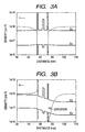
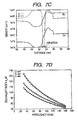
- FIGS. 3A to 3C are band diagrams illustrating how the depletion region is changed in accordance with change of voltage of the electrode 222.
- distance (nm) of the abscissa indicates the positional relationship from the emitter up to the collector through the gain medium 203, and corresponds to the upper and lower directions (lamination direction) in FIGS. 2A and 2B .
- Ec and Ev in FIGS. 3A to 3C respectively represent conduction band edge and valence band edge, and the ordinate indicates arbitrary unit.
- n represents free carrier concentration in conduction band, and the ordinate indicates density (cm -3 ).
- the depletion region is the region of low concentration n ⁇ 1 ⁇ 10 17 cm -3 such that the real part of permittivity becomes positive, which can be considered as dielectric like when viewed from an electromagnetic wave of terahertz band.
- the plasma frequency is a physical quantity indicating the boundary such that medium including free carrier is deemed as metal like when viewed from an electromagnetic wave with a frequency less than that plasma frequency, and is deemed as dielectric like when viewed from an electromagnetic wave with the plasma frequency or more.
- FIG. 3A is a band diagram when voltage of the electrode 222 is 0.0 V.
- FIG. 3B is a band diagram when the voltage of the electrode 222 is 0.4 V
- FIG. 3C is a band diagram when the voltage of the electrode 222 is 0.8 V. It is understood that there is a tendency such that an electric field increases in accordance with increase of voltage, and the depletion region becomes broad in accordance with increase of electric field within the range from 0.0 V to 0.8 V in a manner as stated above.
- the thickness of the depletion region is broadened by about 13 nm as compared to FIG. 3A .
- FIG. 3D illustrates how equivalent refractive index of guided mode immediately below is changed. To realize this, it is sufficient to reflect respective free carrier concentrations of FIGS. 3A, 3B and 3C in the oscillation device configuration with respect to Drude Model to take such a model as a calculation model. To this end, finite element method solver of the Maxwell's equation was used. This method is also a method known by those persons skilled in the art. In this case, from demand of the finite element solver, graded free carrier concentration was not given for the calculation model.
- a, b, c respectively reflect FIGS. 3A 3B and 3C .
- equivalent refractive index of guided mode in the vicinity of, e.g., 0.6 THz is 15.2.
- equivalent refractive index of the guided mode similarly in the vicinity of 0.6 THz is 13.6.
- equivalent refractive index of guided mode similarly in the vicinity of 0.6 Tz is 11.8.
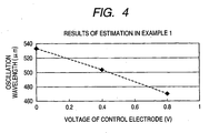
- an oscillation wavelength is estimated.
- 0.4 V is assumed to be applied to the drive electrode 222A, and 0.4 V is assumed to be applied to the control electrode 222B.
- ⁇ , 2 ⁇ 13.6 ⁇ 500/m (m is integer) holds.
- the oscillation wavelength becomes equal to about 500 ⁇ m (0.60 THz) (see FIG. 4 ). It is to be noted that even if many oscillation modes exist in practice, it is sufficient to select wavelength of about 500 ⁇ m by using a filter.
- control electrode 222B when the voltage of control electrode 222B is sweeped in a manner as shown in FIG. 4 , the wavelength variable width becomes equal to about 12%.
- the above-mentioned numeric values are one example. Therefore, control electric field is further greatly changed thus to have ability to further also enlarge wavelength variable width. This is the merit of this example that independent electric fields can be applied to the respective drive and control electrodes 222A and 222B.
- the oscillation device configuration of this example can be fabricated by the following fabrication method.
- the n-InGaAs layers 202, 212, multiple quantum well 203 by InGaAs/AlAs and n-InGaAs layers 211, 201 are epitaxially grown by Molecular Beam Epitaxy (MBE) process on an InP substrate.
- MBE Molecular Beam Epitaxy
- the Ti/Au 221 is deposited on the surface thereof as an electrode to perform etching down to the substrate so as to take a mesa shape in which width is 20 ⁇ m and length is 500 ⁇ as stated above.
- etching there is used dry etching based on photolithography and ICP (Induced Coupling Plasma).
- bonding based on pressure-fitting is performed between the electrode 221 and the Au thin film on the transfer substrate 21 where an Au thin film is deposited.
- wet etching is performed by hydrochloric acid, only the InP substrate is selectively removed. For this reason, there results a form such that the mesa-shaped.epitaxial layer is transferred onto the transfer substrate 21.
- the BCB 22 was coated by spin-coat process. Thereafter, the mesa-shaped epitaxial layer is exposed. Finally, the drive electrode 222A and control electrode 222B were formed, by the lift-off process, on the surface of the n-InGaAs layer 202 which has appeared after the InP substrata has been removed. Thus, the above-mentioned configuration is completed. In this case, for formation of an electrode separation area 223, etching of the n-InGaAs layer 202 may be performed with the photoresist utilized in the lift-off process being as a mask.
- size of the depletion region can be adjusted by a relatively large ratio with respect to the region of the gain medium 203 at a relatively high rate by electric field application through the control electrode 222B as stated above.
- the equivalent refractive index that the guided mode senses can be greatly changed. Accordingly, there can be realized an oscillation device which is broad in wavelength variable width and is high in wavelength sweep rate as compared to the related art.
- FIGS. 5A and 5B illustrate the configuration of the second example of an oscillation device to which the present invention is applied.
- FIG. 5B shows, in an enlarged manner, the device body in FIG. 5A .
- the cavity structure uses DBR. Since the cavity structure having wavelength selectivity is employed as the cavity structure differently from Example 1, mode hopping becomes difficult to take place. Accordingly, as cavity structure forming the oscillation device to which the present invention can be applied, this example is a more desirable example.
- an RTD on the same InP substrate as that of Example 1 is used as a gain medium 503.
- Electrical contacts 511 and 512 are configured so as to include a semiconductor film of n-InGaAs (thickness 50 nm) having electron concentration of 1 ⁇ 10 18 cm -3
- negative permittivity media 501, 502 are configured so as to include a semiconductor film of n-InGaAs (thickness 100 nm) having electron concentration of 1 ⁇ 10 19 cm -3 .
- electrodes 521, 522 522A, 522B, 522C
- DBRs 504, 505 are configured so as to periodically alternately repeat control electrodes 522B, 522C.
- the dimensions of the device body 50 are set so that size in propagation direction of surface plasmon is 1.2 mm, and size in lateral direction thereof is 20 ⁇ m.
- the regions of the DBRs 504, 505 thereof are respectively ensured by about 100 ⁇ m in the propagation direction of surface plasmon.
- the device body 50 includes drive electrode 522A (separated from control electrodes 522B and 522C) by electrode separation regions 523), and the ground electrode 521.
- the DBRs 504, 505 indicate high reflection factor in a specific wavelength depending upon the refractive index distribution period.
- n B is equivalent refractive index that the guided mode immediately below the control electrode 522B senses
- L B is length of surface plasmon waveguide immediately below the control electrode 522B
- n c is equivalent refractive index that guided mode immediately below the control electrode 522C senses
- L c is length of surface plasmon waveguide immediately below the control electrode 522C.
- wavelength variable width becomes equal to about 6 %.
- the above-mentioned numeric values are an example.
- wavelength variable width may be further enlarged. This is because the present example also has the merit to have ability to apply an independent electric field to the drive electrode 522A and control electrodes 522B, 522C.
- the cavity structure configured by periodically repeating control electrodes is caused to be of the DBR type in this example
- the present invention is not limited to such implementation.
- the advantages described in Example 1 can be obtained in addition to the advantages specific to the present example.
- FIGS. 6A and 6B illustrate the configuration of an oscillation device of the third example to which the present invention is applied.
- FIG. 6B illustrates, in an enlarged manner, a device body 60 in FIG. 6A .
- a gain medium is a resonant inter-band tunneling diode (RITD) based on photon-assisted tunneling.
- the RITD has a gain of millimeter wave band utilizing the photon-assisted tunneling. Accordingly, there is disclosed a modified example of a gain medium forming an oscillation device to which the present invention can be applied.
- RITD resonant inter-band tunneling diode
- a gain medium 603 is RITD, and is of the configuration using Type II hetero-junction, e.g., as in the case of n type ⁇ doped part/spacer layer/Type II spacer layer/p-type ⁇ doped part/Type II p-type layer.
- lattice-matched Si may be used on an Si substrate as a spacer layer, and SiGe which is non-matched and serves as Type II hetero-junctioned to Si may be used as a Type II spacer layer or Type II p-type layer.
- a configuration including a semiconductor multilayer structure of n-Si ( ⁇ -dope)/Si (thickness 1.0 nm)/SiGe (2.0 nm)/p-SiGe ( ⁇ -dope)/p-SiGe (1.0 nm) in order from the emitter side to the collector side (see Appl. Phys. Lett, Vol. 83, 3308 (2003 ) in connection with the configuration of gain medium).
- the spacer layer and the Type II spacer layer are caused to be undoped.
- Such gain medium 603 is sandwiched between negative permittivity media 601, 602 doubling as electrical contacts 611, 612.
- the negative permittivity medium 601 is configured so as to include, e.g., a semiconductor film of n-Si (100 nm) which is lattice-matched with an Si substrate.
- P is used as dopant, and electron density is caused to have 5 ⁇ 10 19 cm -3 .
- the negative permittivity medium 602 is configured so as to include, e.g., a semiconductor film of p-Si (100 nm) which is lattice-matched with an Si substrate.
- B is used as dopant, and electron concentration is caused to have 5 ⁇ 10 19 cm -3 .
- the gain medium 603 is in ohmic contact with electrodes 621, 622 (622A, 622B) such as Al.
- the RITD has a gain in a frequency region of millimeter wave band on the basis of phenomenon called photon-assisted tunneling.
- peak current density is about 40 kA/cm 2 at the time of application of an electric field of 0.3V, and indicates negative resistance at the time of application of an electric field of 0.3V to 0.4V.
- dielectric material 62 there is selected a material having low permittivity and small loss such as BCB.
- dimensions of the device body 60 are set such that size in a propagation direction of surface plasmon is 500 ⁇ m, and size in a lateral direction is 20 ⁇ m.
- impedance transformation regions 606, 607 such that equivalent refractive index immediately therebelow is lowered without adding the electrode 622 by ⁇ /4n from the end part of the surface plasmon waveguide.
- This example is directed to an applied example of ⁇ /4 impedance transformation element known in the microwave technology, and is used when there is a desire to enhance coupling efficiency with respect to an external space. It is to be noted that the present invention is not limited to such implementation, but for example, AR coating or lens known in the optical technology may be utilized.
- the device body 60 includes end faces 604, 605, and the ground electrode 621.
- FIGS. 7A to 7C are band diagrams illustrating how the depletion region is changed in accordance with change of the voltage of the electrode 622.
- distance (nm) of the abscissa indicates the positional relationship from the emitter through the gain medium 603 to the collector, and corresponds to upper and lower directions in FIG. 6B .
- n and p respectively indicate free carrier concentrations in the conduction band and the valence band, and the ordinate thereof indicates density (cm -3 ).
- the depletion region is assumed to have low concentration expressed as n ⁇ 1 ⁇ 10 15 cm -3 , p ⁇ 1 ⁇ 10 15 cm -3 such that the real part of permittivity is positive, which is considered as dielectric like when viewed from an electromagnetic wave of millimeter wave band.
- FIG. 7A to 7C illustration is made for easiness of understanding such that the thickness of the depletion region is visually represented as "depletion".
- FIG. 7A is a band diagram when device voltage is 0.0V
- FIG. 7B is a band diagram when device voltage is 0.4V
- FIG. 7C is a diagram when device voltage is 0.8V. It is understood that there is a tendency such that an electric field increases in accordance with increase of voltage, and the depletion region becomes narrow in accordance with increase of electric field within the range from 0.0V to 0.8V as stated above.
- the thickness of the depletion region is narrowed by about 0.2 nm.
- FIG. 7D illustrates how the voltage of the electrode 622 changes the equivalent refractive index of guided mode immediately therebelow.
- respective free carrier concentrations of FIGS. 7A, 7B and 7C in the device configurations are reflected with respect to Drude model so that a calculation model is provided. Calculation was performed within the range from 30 GHz to 160 GHz as an example, wherein frequency (GHz) of the abscissa indicates frequency of fundamental guided mode. The ordinate indicates equivalent refractive index of the fundamental guided mode.
- a, b, c respectively reflect FIGS. 7A, 7B and 7C .
- the equivalent refractive index of the guided mode in the vicinity of 30 GHz is 108, for example.
- the equivalent refractive index of guided mode similarly in the vicinity of, e.g., 30 GHz is 117.
- the equivalent refractive index of the guide wave similarly in the vicinity of 30 GHz is 134.
- the voltage of the electrode 622 is reread as a control electrode 622B voltage as it is, the voltage of a control electrode 622B is swept within the range from 0.0V to 0.8V so that the equivalent refractive index of the guided mode immediately therebelow can be changed within the range from 108 to 134.
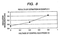
- an oscillation wavelength is estimated.
- 0.4V is applied to a drive electrode 622A and 0.4V is applied to the control electrode 622B.
- the oscillation wavelength becomes equal to about 9.0 mm (33 GHz) (see FIG. 8 ).
- the voltage of the control electrode 622B is swept from 0.0V up to 0.8V so that wavelength variable operation is provided.
- the length L A of the surface plasmon waveguide immediately below the drive electrode 622A is set to 250 ⁇ m
- the length L B of the surface plasmon waveguide immediately below the control electrode 622B is set to 250 ⁇ m.
- the voltage of the control electrode 622B is 0.0V
- the relation expressed as ⁇ 2 ⁇ (117 ⁇ 0.25 + 108 ⁇ 0.25)/13 holds.
- the oscillation wavelength is changed into about 8.7 mm (35 GHz) (see FIG. 8 ).
- voltage of the control electrode 622B is 0.8V
- the relation expressed as ⁇ 2 ⁇ (117 ⁇ 0.25 + 134 ⁇ 0.25)/13 holds.
- the oscillation wavelength is changed into 9.7 mm (31 GHz) (see FIG. 8 ). Accordingly, when the voltage of the control electrode 622B is swept as shown in FIG. 8 , the wavelength variable width becomes equal to about 11 %.
- the above-mentioned numeric values are one example. By further greatly changing control electric field, wavelength variable width may be further enlarged.
- the oscillation device configuration of the present example can be fabricated in accordance with the following fabrication method.
- the p-Si layer 602, the Type II hetero-junction 603 based on Si/SiGe and the n-Si layer 601 are epitaxially grown on an Si substrate by low temperature molecular beam epitaxy (LT-MBE) process.
- LT-MBE low temperature molecular beam epitaxy
- the reason why low temperature growth is selected is to reduce segregation of dopant.
- the Al 621 is deposited as an electrode on the surface thereof to perform etching down to the substrate so as to take a mesa shape in which width is 20 ⁇ m and length is 500 ⁇ m as stated above.
- bonding by pressure-fitting is performed between the electrode 621 and an Al thin film on the transfer substrate 61 where the Al thin film is deposited.
- the mesa-shaped epitaxial layer is transferred onto the transfer substrate 61.
- the BCB 62 is coated thereafter to expose the mesa-shaped epitaxial layer.
- the drive electrode 622A and control electrode 622B are formed on the surface of the p-Si layer 602 which has appeared after the Si substrate has been removed.
- Example 1 the advantages which have been described in Example 1 similarly including Fabry-Perot etalon cavity can be provided.
Landscapes
- Physics & Mathematics (AREA)
- Electromagnetism (AREA)
- Optics & Photonics (AREA)
- Engineering & Computer Science (AREA)
- Condensed Matter Physics & Semiconductors (AREA)
- General Physics & Mathematics (AREA)
- Nanotechnology (AREA)
- Chemical & Material Sciences (AREA)
- Biophysics (AREA)
- Crystallography & Structural Chemistry (AREA)
- Life Sciences & Earth Sciences (AREA)
- Semiconductor Lasers (AREA)
- Optical Modulation, Optical Deflection, Nonlinear Optics, Optical Demodulation, Optical Logic Elements (AREA)
- Lasers (AREA)
Applications Claiming Priority (2)
| Application Number | Priority Date | Filing Date | Title |
|---|---|---|---|
| JP2006344565 | 2006-12-21 | ||
| PCT/JP2007/075234 WO2008075795A1 (en) | 2006-12-21 | 2007-12-20 | Electrically tunable terahertz laser oscillation device |
Publications (2)
| Publication Number | Publication Date |
|---|---|
| EP2067217A1 EP2067217A1 (en) | 2009-06-10 |
| EP2067217B1 true EP2067217B1 (en) | 2013-10-02 |
Family
ID=39202173
Family Applications (1)
| Application Number | Title | Priority Date | Filing Date |
|---|---|---|---|
| EP07851121.9A Not-in-force EP2067217B1 (en) | 2006-12-21 | 2007-12-20 | Electrically tunable terahertz laser oscillation device |
Country Status (5)
| Country | Link |
|---|---|
| US (1) | US7889015B2 (enExample) |
| EP (1) | EP2067217B1 (enExample) |
| JP (1) | JP4873746B2 (enExample) |
| CN (1) | CN101512850B (enExample) |
| WO (1) | WO2008075795A1 (enExample) |
Families Citing this family (16)
| Publication number | Priority date | Publication date | Assignee | Title |
|---|---|---|---|---|
| JP4871816B2 (ja) | 2007-08-31 | 2012-02-08 | キヤノン株式会社 | レーザ素子 |
| JP4807707B2 (ja) * | 2007-11-30 | 2011-11-02 | キヤノン株式会社 | 波形情報取得装置 |
| JP5506258B2 (ja) * | 2008-08-06 | 2014-05-28 | キヤノン株式会社 | 整流素子 |
| JP5665305B2 (ja) * | 2008-12-25 | 2015-02-04 | キヤノン株式会社 | 分析装置 |
| JP5632599B2 (ja) | 2009-09-07 | 2014-11-26 | キヤノン株式会社 | 発振器 |
| JP5632598B2 (ja) | 2009-09-07 | 2014-11-26 | キヤノン株式会社 | 発振回路及び発振器 |
| JP5612842B2 (ja) | 2009-09-07 | 2014-10-22 | キヤノン株式会社 | 発振器 |
| US8532152B2 (en) * | 2009-11-03 | 2013-09-10 | Massachusetts Institute Of Technology | Frequency tunable wire lasers |
| KR20120087631A (ko) | 2011-01-28 | 2012-08-07 | 삼성전자주식회사 | 나노 구조화된 음향광학 소자, 및 상기 음향광학 소자를 이용한 광 스캐너, 광 변조기 및 홀로그래픽 디스플레이 장치 |
| JP6280310B2 (ja) | 2012-06-06 | 2018-02-14 | キヤノン株式会社 | 発振器 |
| JP2014175533A (ja) * | 2013-03-11 | 2014-09-22 | Canon Inc | レーザ素子 |
| JP6373010B2 (ja) | 2013-03-12 | 2018-08-15 | キヤノン株式会社 | 発振素子 |
| JP2014207654A (ja) * | 2013-03-16 | 2014-10-30 | キヤノン株式会社 | 導波路素子 |
| JP6464895B2 (ja) * | 2015-04-03 | 2019-02-06 | 住友電気工業株式会社 | 量子カスケード半導体レーザ |
| KR101910983B1 (ko) * | 2017-10-24 | 2018-10-23 | 삼성전자주식회사 | 나노 구조화된 음향광학 소자, 및 상기 음향광학 소자를 이용한 광 스캐너, 광 변조기 및 홀로그래픽 디스플레이 장치 |
| US11031753B1 (en) * | 2017-11-13 | 2021-06-08 | The Government Of The United States Of America As Represented By The Secretary Of The Air Force | Extracting the fundamental mode in broad area quantum cascade lasers |
Family Cites Families (26)
| Publication number | Priority date | Publication date | Assignee | Title |
|---|---|---|---|---|
| JP3210159B2 (ja) | 1993-12-10 | 2001-09-17 | キヤノン株式会社 | 半導体レーザ、光源装置、光通信システム及び光通信方法 |
| JPH07307530A (ja) | 1994-03-17 | 1995-11-21 | Canon Inc | 偏波変調可能な半導体レーザ |
| US5659560A (en) | 1994-05-12 | 1997-08-19 | Canon Kabushiki Kaisha | Apparatus and method for driving oscillation polarization selective light source, and optical communication system using the same |
| US5764670A (en) * | 1995-02-27 | 1998-06-09 | Canon Kabushiki Kaisha | Semiconductor laser apparatus requiring no external modulator, method of driving semiconductor laser device, and optical communication system using the semiconductor laser apparatus |
| US5978397A (en) * | 1997-03-27 | 1999-11-02 | Lucent Technologies Inc. | Article comprising an electric field-tunable semiconductor laser |
| US6301282B1 (en) | 1998-07-29 | 2001-10-09 | Lucent Technologies Inc. | Long wavelength semiconductor lasers incorporating waveguides based on surface plasmons |
| JP2001042170A (ja) | 1999-07-28 | 2001-02-16 | Canon Inc | 光配線装置、その駆動方法およびそれを用いた電子機器 |
| US7630588B2 (en) | 2003-06-25 | 2009-12-08 | Canon Kabushiki Kaisha | High frequency electrical signal control device and sensing system |
| US20050058166A1 (en) * | 2003-09-12 | 2005-03-17 | Qing Hu | Metal waveguides for mode confinement in terahertz lasers and amplifiers |
| JP4136858B2 (ja) | 2003-09-12 | 2008-08-20 | キヤノン株式会社 | 位置検出装置、及び情報入力装置 |
| JP2005157601A (ja) | 2003-11-25 | 2005-06-16 | Canon Inc | 電磁波による積層状物体計数装置及び計数方法 |
| JP4217646B2 (ja) | 2004-03-26 | 2009-02-04 | キヤノン株式会社 | 認証方法及び認証装置 |
| US7301977B2 (en) | 2004-06-10 | 2007-11-27 | Nanoplus Gmbh | Tuneable unipolar lasers |
| JP4250573B2 (ja) | 2004-07-16 | 2009-04-08 | キヤノン株式会社 | 素子 |
| JP4546326B2 (ja) | 2004-07-30 | 2010-09-15 | キヤノン株式会社 | センシング装置 |
| JP4390147B2 (ja) | 2005-03-28 | 2009-12-24 | キヤノン株式会社 | 周波数可変発振器 |
| JP4250603B2 (ja) | 2005-03-28 | 2009-04-08 | キヤノン株式会社 | テラヘルツ波の発生素子、及びその製造方法 |
| JP2006275910A (ja) | 2005-03-30 | 2006-10-12 | Canon Inc | 位置センシング装置及び位置センシング方法 |
| US7349456B2 (en) * | 2005-10-07 | 2008-03-25 | Agilent Technologies, Inc. | Gain-coupled distributed quantum cascade laser |
| JP4773839B2 (ja) | 2006-02-15 | 2011-09-14 | キヤノン株式会社 | 対象物の情報を検出する検出装置 |
| JP5132146B2 (ja) | 2006-03-17 | 2013-01-30 | キヤノン株式会社 | 分析方法、分析装置、及び検体保持部材 |
| JP4481946B2 (ja) | 2006-03-17 | 2010-06-16 | キヤノン株式会社 | 検出素子及び画像形成装置 |
| JP4898472B2 (ja) | 2006-04-11 | 2012-03-14 | キヤノン株式会社 | 検査装置 |
| JP4709059B2 (ja) | 2006-04-28 | 2011-06-22 | キヤノン株式会社 | 検査装置及び検査方法 |
| JP4857027B2 (ja) * | 2006-05-31 | 2012-01-18 | キヤノン株式会社 | レーザ素子 |
| JP5196750B2 (ja) | 2006-08-25 | 2013-05-15 | キヤノン株式会社 | 発振素子 |
-
2007
- 2007-12-10 JP JP2007318581A patent/JP4873746B2/ja not_active Expired - Fee Related
- 2007-12-20 CN CN200780032896XA patent/CN101512850B/zh not_active Expired - Fee Related
- 2007-12-20 EP EP07851121.9A patent/EP2067217B1/en not_active Not-in-force
- 2007-12-20 WO PCT/JP2007/075234 patent/WO2008075795A1/en not_active Ceased
- 2007-12-20 US US12/091,393 patent/US7889015B2/en not_active Expired - Fee Related
Also Published As
| Publication number | Publication date |
|---|---|
| CN101512850A (zh) | 2009-08-19 |
| WO2008075795A1 (en) | 2008-06-26 |
| US7889015B2 (en) | 2011-02-15 |
| CN101512850B (zh) | 2011-08-31 |
| US20100164636A1 (en) | 2010-07-01 |
| EP2067217A1 (en) | 2009-06-10 |
| JP2008177551A (ja) | 2008-07-31 |
| WO2008075795B1 (en) | 2008-09-12 |
| JP4873746B2 (ja) | 2012-02-08 |
Similar Documents
| Publication | Publication Date | Title |
|---|---|---|
| EP2067217B1 (en) | Electrically tunable terahertz laser oscillation device | |
| Abdollahinia et al. | Temperature stability of static and dynamic properties of 1.55 µm quantum dot lasers | |
| US7693198B2 (en) | Laser device | |
| US7839910B2 (en) | Laser device | |
| US5727010A (en) | Article comprising an improved quantum cascade laser | |
| EP2525449A2 (en) | Waveguide, apparatus including the waveguide, and method of manufacturing the waveguide | |
| EP2198491B1 (en) | Laser device | |
| EP2528171A1 (en) | Waveguide, apparatus including the waveguide, and method of manufacturing the waveguide | |
| US7382806B2 (en) | THz semiconductor laser incorporating a controlled plasmon confinement waveguide | |
| Ohtani et al. | Electrical laser frequency tuning by three terminal terahertz quantum cascade lasers | |
| Suchalkin et al. | Widely tunable type-II interband cascade laser | |
| Tredicucci et al. | Terahertz quantum cascade lasers | |
| Ohtani et al. | Above room-temperature operation of InAs∕ AlGaSb superlattice quantum cascade lasers emitting at 12μm | |
| Yang et al. | Distributed-feedback GaInAs∕ AlAsSb quantum-cascade lasers operating at 300K | |
| JPH0642585B2 (ja) | 半導体レーザ | |
| Vasko et al. | Heterostructure-based optoelectronic devices | |
| Hofstetter et al. | GaN/AlN-based electro-optical modulator for 1.55 µm using intersubband transitions WOCSDICE 2006, Fiskebäckskil, Sweden | |
| Vurgaftman et al. | Edge-and surface-emitting photonic-crystal distributed-feedback lasers |
Legal Events
| Date | Code | Title | Description |
|---|---|---|---|
| PUAI | Public reference made under article 153(3) epc to a published international application that has entered the european phase |
Free format text: ORIGINAL CODE: 0009012 |
|
| 17P | Request for examination filed |
Effective date: 20090313 |
|
| AK | Designated contracting states |
Kind code of ref document: A1 Designated state(s): AT BE BG CH CY CZ DE DK EE ES FI FR GB GR HU IE IS IT LI LT LU LV MC MT NL PL PT RO SE SI SK TR |
|
| AX | Request for extension of the european patent |
Extension state: AL BA HR MK RS |
|
| 17Q | First examination report despatched |
Effective date: 20090713 |
|
| DAX | Request for extension of the european patent (deleted) | ||
| GRAP | Despatch of communication of intention to grant a patent |
Free format text: ORIGINAL CODE: EPIDOSNIGR1 |
|
| GRAP | Despatch of communication of intention to grant a patent |
Free format text: ORIGINAL CODE: EPIDOSNIGR1 |
|
| INTG | Intention to grant announced |
Effective date: 20130718 |
|
| GRAS | Grant fee paid |
Free format text: ORIGINAL CODE: EPIDOSNIGR3 |
|
| GRAA | (expected) grant |
Free format text: ORIGINAL CODE: 0009210 |
|
| AK | Designated contracting states |
Kind code of ref document: B1 Designated state(s): AT BE BG CH CY CZ DE DK EE ES FI FR GB GR HU IE IS IT LI LT LU LV MC MT NL PL PT RO SE SI SK TR |
|
| REG | Reference to a national code |
Ref country code: GB Ref legal event code: FG4D |
|
| REG | Reference to a national code |
Ref country code: AT Ref legal event code: REF Ref document number: 635022 Country of ref document: AT Kind code of ref document: T Effective date: 20131015 Ref country code: CH Ref legal event code: EP |
|
| REG | Reference to a national code |
Ref country code: IE Ref legal event code: FG4D |
|
| REG | Reference to a national code |
Ref country code: DE Ref legal event code: R096 Ref document number: 602007033175 Country of ref document: DE Effective date: 20131128 |
|
| REG | Reference to a national code |
Ref country code: AT Ref legal event code: MK05 Ref document number: 635022 Country of ref document: AT Kind code of ref document: T Effective date: 20131002 |
|
| REG | Reference to a national code |
Ref country code: NL Ref legal event code: VDEP Effective date: 20131002 |
|
| PG25 | Lapsed in a contracting state [announced via postgrant information from national office to epo] |
Ref country code: SI Free format text: LAPSE BECAUSE OF FAILURE TO SUBMIT A TRANSLATION OF THE DESCRIPTION OR TO PAY THE FEE WITHIN THE PRESCRIBED TIME-LIMIT Effective date: 20131002 |
|
| REG | Reference to a national code |
Ref country code: LT Ref legal event code: MG4D |
|
| PG25 | Lapsed in a contracting state [announced via postgrant information from national office to epo] |
Ref country code: NL Free format text: LAPSE BECAUSE OF FAILURE TO SUBMIT A TRANSLATION OF THE DESCRIPTION OR TO PAY THE FEE WITHIN THE PRESCRIBED TIME-LIMIT Effective date: 20131002 Ref country code: IS Free format text: LAPSE BECAUSE OF FAILURE TO SUBMIT A TRANSLATION OF THE DESCRIPTION OR TO PAY THE FEE WITHIN THE PRESCRIBED TIME-LIMIT Effective date: 20140202 Ref country code: LT Free format text: LAPSE BECAUSE OF FAILURE TO SUBMIT A TRANSLATION OF THE DESCRIPTION OR TO PAY THE FEE WITHIN THE PRESCRIBED TIME-LIMIT Effective date: 20131002 Ref country code: FI Free format text: LAPSE BECAUSE OF FAILURE TO SUBMIT A TRANSLATION OF THE DESCRIPTION OR TO PAY THE FEE WITHIN THE PRESCRIBED TIME-LIMIT Effective date: 20131002 Ref country code: SE Free format text: LAPSE BECAUSE OF FAILURE TO SUBMIT A TRANSLATION OF THE DESCRIPTION OR TO PAY THE FEE WITHIN THE PRESCRIBED TIME-LIMIT Effective date: 20131002 Ref country code: BE Free format text: LAPSE BECAUSE OF FAILURE TO SUBMIT A TRANSLATION OF THE DESCRIPTION OR TO PAY THE FEE WITHIN THE PRESCRIBED TIME-LIMIT Effective date: 20131002 Ref country code: CZ Free format text: LAPSE BECAUSE OF FAILURE TO SUBMIT A TRANSLATION OF THE DESCRIPTION OR TO PAY THE FEE WITHIN THE PRESCRIBED TIME-LIMIT Effective date: 20131002 |
|
| PG25 | Lapsed in a contracting state [announced via postgrant information from national office to epo] |
Ref country code: AT Free format text: LAPSE BECAUSE OF FAILURE TO SUBMIT A TRANSLATION OF THE DESCRIPTION OR TO PAY THE FEE WITHIN THE PRESCRIBED TIME-LIMIT Effective date: 20131002 Ref country code: ES Free format text: LAPSE BECAUSE OF FAILURE TO SUBMIT A TRANSLATION OF THE DESCRIPTION OR TO PAY THE FEE WITHIN THE PRESCRIBED TIME-LIMIT Effective date: 20131002 Ref country code: PL Free format text: LAPSE BECAUSE OF FAILURE TO SUBMIT A TRANSLATION OF THE DESCRIPTION OR TO PAY THE FEE WITHIN THE PRESCRIBED TIME-LIMIT Effective date: 20131002 Ref country code: LV Free format text: LAPSE BECAUSE OF FAILURE TO SUBMIT A TRANSLATION OF THE DESCRIPTION OR TO PAY THE FEE WITHIN THE PRESCRIBED TIME-LIMIT Effective date: 20131002 Ref country code: CY Free format text: LAPSE BECAUSE OF FAILURE TO SUBMIT A TRANSLATION OF THE DESCRIPTION OR TO PAY THE FEE WITHIN THE PRESCRIBED TIME-LIMIT Effective date: 20131002 |
|
| PG25 | Lapsed in a contracting state [announced via postgrant information from national office to epo] |
Ref country code: PT Free format text: LAPSE BECAUSE OF FAILURE TO SUBMIT A TRANSLATION OF THE DESCRIPTION OR TO PAY THE FEE WITHIN THE PRESCRIBED TIME-LIMIT Effective date: 20140203 |
|
| REG | Reference to a national code |
Ref country code: DE Ref legal event code: R097 Ref document number: 602007033175 Country of ref document: DE |
|
| PG25 | Lapsed in a contracting state [announced via postgrant information from national office to epo] |
Ref country code: EE Free format text: LAPSE BECAUSE OF FAILURE TO SUBMIT A TRANSLATION OF THE DESCRIPTION OR TO PAY THE FEE WITHIN THE PRESCRIBED TIME-LIMIT Effective date: 20131002 |
|
| REG | Reference to a national code |
Ref country code: CH Ref legal event code: PL |
|
| PLBE | No opposition filed within time limit |
Free format text: ORIGINAL CODE: 0009261 |
|
| STAA | Information on the status of an ep patent application or granted ep patent |
Free format text: STATUS: NO OPPOSITION FILED WITHIN TIME LIMIT |
|
| PG25 | Lapsed in a contracting state [announced via postgrant information from national office to epo] |
Ref country code: LU Free format text: LAPSE BECAUSE OF FAILURE TO SUBMIT A TRANSLATION OF THE DESCRIPTION OR TO PAY THE FEE WITHIN THE PRESCRIBED TIME-LIMIT Effective date: 20131220 Ref country code: MC Free format text: LAPSE BECAUSE OF FAILURE TO SUBMIT A TRANSLATION OF THE DESCRIPTION OR TO PAY THE FEE WITHIN THE PRESCRIBED TIME-LIMIT Effective date: 20131002 Ref country code: SK Free format text: LAPSE BECAUSE OF FAILURE TO SUBMIT A TRANSLATION OF THE DESCRIPTION OR TO PAY THE FEE WITHIN THE PRESCRIBED TIME-LIMIT Effective date: 20131002 Ref country code: IT Free format text: LAPSE BECAUSE OF FAILURE TO SUBMIT A TRANSLATION OF THE DESCRIPTION OR TO PAY THE FEE WITHIN THE PRESCRIBED TIME-LIMIT Effective date: 20131002 Ref country code: RO Free format text: LAPSE BECAUSE OF FAILURE TO SUBMIT A TRANSLATION OF THE DESCRIPTION OR TO PAY THE FEE WITHIN THE PRESCRIBED TIME-LIMIT Effective date: 20131002 |
|
| 26N | No opposition filed |
Effective date: 20140703 |
|
| REG | Reference to a national code |
Ref country code: IE Ref legal event code: MM4A |
|
| REG | Reference to a national code |
Ref country code: FR Ref legal event code: ST Effective date: 20140829 |
|
| PG25 | Lapsed in a contracting state [announced via postgrant information from national office to epo] |
Ref country code: DK Free format text: LAPSE BECAUSE OF FAILURE TO SUBMIT A TRANSLATION OF THE DESCRIPTION OR TO PAY THE FEE WITHIN THE PRESCRIBED TIME-LIMIT Effective date: 20131002 |
|
| REG | Reference to a national code |
Ref country code: DE Ref legal event code: R097 Ref document number: 602007033175 Country of ref document: DE Effective date: 20140703 |
|
| PG25 | Lapsed in a contracting state [announced via postgrant information from national office to epo] |
Ref country code: LI Free format text: LAPSE BECAUSE OF NON-PAYMENT OF DUE FEES Effective date: 20131231 Ref country code: IE Free format text: LAPSE BECAUSE OF NON-PAYMENT OF DUE FEES Effective date: 20131220 Ref country code: CH Free format text: LAPSE BECAUSE OF NON-PAYMENT OF DUE FEES Effective date: 20131231 |
|
| PG25 | Lapsed in a contracting state [announced via postgrant information from national office to epo] |
Ref country code: FR Free format text: LAPSE BECAUSE OF NON-PAYMENT OF DUE FEES Effective date: 20131231 |
|
| PG25 | Lapsed in a contracting state [announced via postgrant information from national office to epo] |
Ref country code: TR Free format text: LAPSE BECAUSE OF FAILURE TO SUBMIT A TRANSLATION OF THE DESCRIPTION OR TO PAY THE FEE WITHIN THE PRESCRIBED TIME-LIMIT Effective date: 20131002 |
|
| PG25 | Lapsed in a contracting state [announced via postgrant information from national office to epo] |
Ref country code: BG Free format text: LAPSE BECAUSE OF FAILURE TO SUBMIT A TRANSLATION OF THE DESCRIPTION OR TO PAY THE FEE WITHIN THE PRESCRIBED TIME-LIMIT Effective date: 20131002 Ref country code: HU Free format text: LAPSE BECAUSE OF FAILURE TO SUBMIT A TRANSLATION OF THE DESCRIPTION OR TO PAY THE FEE WITHIN THE PRESCRIBED TIME-LIMIT; INVALID AB INITIO Effective date: 20071220 |
|
| PG25 | Lapsed in a contracting state [announced via postgrant information from national office to epo] |
Ref country code: GR Free format text: LAPSE BECAUSE OF NON-PAYMENT OF DUE FEES Effective date: 20131002 Ref country code: MT Free format text: LAPSE BECAUSE OF FAILURE TO SUBMIT A TRANSLATION OF THE DESCRIPTION OR TO PAY THE FEE WITHIN THE PRESCRIBED TIME-LIMIT Effective date: 20131002 |
|
| PG25 | Lapsed in a contracting state [announced via postgrant information from national office to epo] |
Ref country code: GR Free format text: LAPSE BECAUSE OF FAILURE TO SUBMIT A TRANSLATION OF THE DESCRIPTION OR TO PAY THE FEE WITHIN THE PRESCRIBED TIME-LIMIT Effective date: 20140103 |
|
| PGFP | Annual fee paid to national office [announced via postgrant information from national office to epo] |
Ref country code: GB Payment date: 20161230 Year of fee payment: 10 |
|
| PGFP | Annual fee paid to national office [announced via postgrant information from national office to epo] |
Ref country code: DE Payment date: 20161231 Year of fee payment: 10 |
|
| REG | Reference to a national code |
Ref country code: DE Ref legal event code: R119 Ref document number: 602007033175 Country of ref document: DE |
|
| GBPC | Gb: european patent ceased through non-payment of renewal fee |
Effective date: 20171220 |
|
| PG25 | Lapsed in a contracting state [announced via postgrant information from national office to epo] |
Ref country code: DE Free format text: LAPSE BECAUSE OF NON-PAYMENT OF DUE FEES Effective date: 20180703 |
|
| PG25 | Lapsed in a contracting state [announced via postgrant information from national office to epo] |
Ref country code: GB Free format text: LAPSE BECAUSE OF NON-PAYMENT OF DUE FEES Effective date: 20171220 |