EP2058679A2 - Dispositif d'émission, dispositif de source lumineuse de surface et affichage - Google Patents
Dispositif d'émission, dispositif de source lumineuse de surface et affichage Download PDFInfo
- Publication number
- EP2058679A2 EP2058679A2 EP08168091A EP08168091A EP2058679A2 EP 2058679 A2 EP2058679 A2 EP 2058679A2 EP 08168091 A EP08168091 A EP 08168091A EP 08168091 A EP08168091 A EP 08168091A EP 2058679 A2 EP2058679 A2 EP 2058679A2
- Authority
- EP
- European Patent Office
- Prior art keywords
- light
- emission
- recess portion
- recess
- slope
- Prior art date
- Legal status (The legal status is an assumption and is not a legal conclusion. Google has not performed a legal analysis and makes no representation as to the accuracy of the status listed.)
- Granted
Links
- 230000004907 flux Effects 0.000 claims abstract description 145
- 230000003287 optical effect Effects 0.000 claims abstract description 72
- 238000005286 illumination Methods 0.000 claims abstract description 33
- 238000009792 diffusion process Methods 0.000 claims description 38
- 230000000452 restraining effect Effects 0.000 claims description 2
- 230000004048 modification Effects 0.000 description 29
- 238000012986 modification Methods 0.000 description 29
- 239000000758 substrate Substances 0.000 description 14
- 238000010586 diagram Methods 0.000 description 11
- 238000009826 distribution Methods 0.000 description 8
- 239000000463 material Substances 0.000 description 4
- 229920003229 poly(methyl methacrylate) Polymers 0.000 description 4
- 239000004417 polycarbonate Substances 0.000 description 4
- 239000004926 polymethyl methacrylate Substances 0.000 description 4
- 238000004088 simulation Methods 0.000 description 4
- 238000005520 cutting process Methods 0.000 description 3
- 230000000694 effects Effects 0.000 description 3
- 239000011347 resin Substances 0.000 description 3
- 229920005989 resin Polymers 0.000 description 3
- 230000009471 action Effects 0.000 description 2
- 238000003491 array Methods 0.000 description 2
- 239000004973 liquid crystal related substance Substances 0.000 description 2
- 239000011159 matrix material Substances 0.000 description 2
- 239000002245 particle Substances 0.000 description 2
- 229920000515 polycarbonate Polymers 0.000 description 2
- 230000009467 reduction Effects 0.000 description 2
- GWEVSGVZZGPLCZ-UHFFFAOYSA-N Titan oxide Chemical compound O=[Ti]=O GWEVSGVZZGPLCZ-UHFFFAOYSA-N 0.000 description 1
- 239000000853 adhesive Substances 0.000 description 1
- 230000001070 adhesive effect Effects 0.000 description 1
- 238000004364 calculation method Methods 0.000 description 1
- 239000011248 coating agent Substances 0.000 description 1
- 238000000576 coating method Methods 0.000 description 1
- 239000003086 colorant Substances 0.000 description 1
- 125000004122 cyclic group Chemical group 0.000 description 1
- 239000003822 epoxy resin Substances 0.000 description 1
- 239000010419 fine particle Substances 0.000 description 1
- 239000011521 glass Substances 0.000 description 1
- 238000004519 manufacturing process Methods 0.000 description 1
- 238000005259 measurement Methods 0.000 description 1
- 238000000034 method Methods 0.000 description 1
- 239000011859 microparticle Substances 0.000 description 1
- 229920000647 polyepoxide Polymers 0.000 description 1
- 229920001296 polysiloxane Polymers 0.000 description 1
- 230000008569 process Effects 0.000 description 1
- 238000009877 rendering Methods 0.000 description 1
Images


Classifications
-
- G—PHYSICS
- G02—OPTICS
- G02F—OPTICAL DEVICES OR ARRANGEMENTS FOR THE CONTROL OF LIGHT BY MODIFICATION OF THE OPTICAL PROPERTIES OF THE MEDIA OF THE ELEMENTS INVOLVED THEREIN; NON-LINEAR OPTICS; FREQUENCY-CHANGING OF LIGHT; OPTICAL LOGIC ELEMENTS; OPTICAL ANALOGUE/DIGITAL CONVERTERS
- G02F1/00—Devices or arrangements for the control of the intensity, colour, phase, polarisation or direction of light arriving from an independent light source, e.g. switching, gating or modulating; Non-linear optics
- G02F1/01—Devices or arrangements for the control of the intensity, colour, phase, polarisation or direction of light arriving from an independent light source, e.g. switching, gating or modulating; Non-linear optics for the control of the intensity, phase, polarisation or colour
- G02F1/13—Devices or arrangements for the control of the intensity, colour, phase, polarisation or direction of light arriving from an independent light source, e.g. switching, gating or modulating; Non-linear optics for the control of the intensity, phase, polarisation or colour based on liquid crystals, e.g. single liquid crystal display cells
- G02F1/133—Constructional arrangements; Operation of liquid crystal cells; Circuit arrangements
- G02F1/1333—Constructional arrangements; Manufacturing methods
- G02F1/1335—Structural association of cells with optical devices, e.g. polarisers or reflectors
- G02F1/1336—Illuminating devices
- G02F1/133602—Direct backlight
- G02F1/133603—Direct backlight with LEDs
-
- F—MECHANICAL ENGINEERING; LIGHTING; HEATING; WEAPONS; BLASTING
- F21—LIGHTING
- F21V—FUNCTIONAL FEATURES OR DETAILS OF LIGHTING DEVICES OR SYSTEMS THEREOF; STRUCTURAL COMBINATIONS OF LIGHTING DEVICES WITH OTHER ARTICLES, NOT OTHERWISE PROVIDED FOR
- F21V5/00—Refractors for light sources
- F21V5/04—Refractors for light sources of lens shape
- F21V5/048—Refractors for light sources of lens shape the lens being a simple lens adapted to cooperate with a point-like source for emitting mainly in one direction and having an axis coincident with the main light transmission direction, e.g. convergent or divergent lenses, plano-concave or plano-convex lenses
-
- G—PHYSICS
- G02—OPTICS
- G02B—OPTICAL ELEMENTS, SYSTEMS OR APPARATUS
- G02B19/00—Condensers, e.g. light collectors or similar non-imaging optics
- G02B19/0004—Condensers, e.g. light collectors or similar non-imaging optics characterised by the optical means employed
- G02B19/0009—Condensers, e.g. light collectors or similar non-imaging optics characterised by the optical means employed having refractive surfaces only
- G02B19/0014—Condensers, e.g. light collectors or similar non-imaging optics characterised by the optical means employed having refractive surfaces only at least one surface having optical power
-
- G—PHYSICS
- G02—OPTICS
- G02B—OPTICAL ELEMENTS, SYSTEMS OR APPARATUS
- G02B19/00—Condensers, e.g. light collectors or similar non-imaging optics
- G02B19/0033—Condensers, e.g. light collectors or similar non-imaging optics characterised by the use
- G02B19/0047—Condensers, e.g. light collectors or similar non-imaging optics characterised by the use for use with a light source
- G02B19/0061—Condensers, e.g. light collectors or similar non-imaging optics characterised by the use for use with a light source the light source comprising a LED
-
- G—PHYSICS
- G02—OPTICS
- G02B—OPTICAL ELEMENTS, SYSTEMS OR APPARATUS
- G02B27/00—Optical systems or apparatus not provided for by any of the groups G02B1/00 - G02B26/00, G02B30/00
- G02B27/09—Beam shaping, e.g. changing the cross-sectional area, not otherwise provided for
- G02B27/0938—Using specific optical elements
- G02B27/095—Refractive optical elements
- G02B27/0955—Lenses
-
- G—PHYSICS
- G02—OPTICS
- G02B—OPTICAL ELEMENTS, SYSTEMS OR APPARATUS
- G02B3/00—Simple or compound lenses
- G02B3/02—Simple or compound lenses with non-spherical faces
- G02B3/04—Simple or compound lenses with non-spherical faces with continuous faces that are rotationally symmetrical but deviate from a true sphere, e.g. so called "aspheric" lenses
-
- G—PHYSICS
- G02—OPTICS
- G02B—OPTICAL ELEMENTS, SYSTEMS OR APPARATUS
- G02B3/00—Simple or compound lenses
- G02B3/02—Simple or compound lenses with non-spherical faces
- G02B3/08—Simple or compound lenses with non-spherical faces with discontinuous faces, e.g. Fresnel lens
-
- G—PHYSICS
- G02—OPTICS
- G02F—OPTICAL DEVICES OR ARRANGEMENTS FOR THE CONTROL OF LIGHT BY MODIFICATION OF THE OPTICAL PROPERTIES OF THE MEDIA OF THE ELEMENTS INVOLVED THEREIN; NON-LINEAR OPTICS; FREQUENCY-CHANGING OF LIGHT; OPTICAL LOGIC ELEMENTS; OPTICAL ANALOGUE/DIGITAL CONVERTERS
- G02F1/00—Devices or arrangements for the control of the intensity, colour, phase, polarisation or direction of light arriving from an independent light source, e.g. switching, gating or modulating; Non-linear optics
- G02F1/01—Devices or arrangements for the control of the intensity, colour, phase, polarisation or direction of light arriving from an independent light source, e.g. switching, gating or modulating; Non-linear optics for the control of the intensity, phase, polarisation or colour
- G02F1/13—Devices or arrangements for the control of the intensity, colour, phase, polarisation or direction of light arriving from an independent light source, e.g. switching, gating or modulating; Non-linear optics for the control of the intensity, phase, polarisation or colour based on liquid crystals, e.g. single liquid crystal display cells
- G02F1/133—Constructional arrangements; Operation of liquid crystal cells; Circuit arrangements
- G02F1/1333—Constructional arrangements; Manufacturing methods
- G02F1/1335—Structural association of cells with optical devices, e.g. polarisers or reflectors
- G02F1/1336—Illuminating devices
- G02F1/133602—Direct backlight
- G02F1/133606—Direct backlight including a specially adapted diffusing, scattering or light controlling members
-
- G—PHYSICS
- G02—OPTICS
- G02F—OPTICAL DEVICES OR ARRANGEMENTS FOR THE CONTROL OF LIGHT BY MODIFICATION OF THE OPTICAL PROPERTIES OF THE MEDIA OF THE ELEMENTS INVOLVED THEREIN; NON-LINEAR OPTICS; FREQUENCY-CHANGING OF LIGHT; OPTICAL LOGIC ELEMENTS; OPTICAL ANALOGUE/DIGITAL CONVERTERS
- G02F1/00—Devices or arrangements for the control of the intensity, colour, phase, polarisation or direction of light arriving from an independent light source, e.g. switching, gating or modulating; Non-linear optics
- G02F1/01—Devices or arrangements for the control of the intensity, colour, phase, polarisation or direction of light arriving from an independent light source, e.g. switching, gating or modulating; Non-linear optics for the control of the intensity, phase, polarisation or colour
- G02F1/13—Devices or arrangements for the control of the intensity, colour, phase, polarisation or direction of light arriving from an independent light source, e.g. switching, gating or modulating; Non-linear optics for the control of the intensity, phase, polarisation or colour based on liquid crystals, e.g. single liquid crystal display cells
- G02F1/133—Constructional arrangements; Operation of liquid crystal cells; Circuit arrangements
- G02F1/1333—Constructional arrangements; Manufacturing methods
- G02F1/1335—Structural association of cells with optical devices, e.g. polarisers or reflectors
- G02F1/1336—Illuminating devices
- G02F1/133602—Direct backlight
- G02F1/133611—Direct backlight including means for improving the brightness uniformity
-
- F—MECHANICAL ENGINEERING; LIGHTING; HEATING; WEAPONS; BLASTING
- F21—LIGHTING
- F21Y—INDEXING SCHEME ASSOCIATED WITH SUBCLASSES F21K, F21L, F21S and F21V, RELATING TO THE FORM OR THE KIND OF THE LIGHT SOURCES OR OF THE COLOUR OF THE LIGHT EMITTED
- F21Y2115/00—Light-generating elements of semiconductor light sources
- F21Y2115/10—Light-emitting diodes [LED]
-
- G—PHYSICS
- G02—OPTICS
- G02F—OPTICAL DEVICES OR ARRANGEMENTS FOR THE CONTROL OF LIGHT BY MODIFICATION OF THE OPTICAL PROPERTIES OF THE MEDIA OF THE ELEMENTS INVOLVED THEREIN; NON-LINEAR OPTICS; FREQUENCY-CHANGING OF LIGHT; OPTICAL LOGIC ELEMENTS; OPTICAL ANALOGUE/DIGITAL CONVERTERS
- G02F1/00—Devices or arrangements for the control of the intensity, colour, phase, polarisation or direction of light arriving from an independent light source, e.g. switching, gating or modulating; Non-linear optics
- G02F1/01—Devices or arrangements for the control of the intensity, colour, phase, polarisation or direction of light arriving from an independent light source, e.g. switching, gating or modulating; Non-linear optics for the control of the intensity, phase, polarisation or colour
- G02F1/13—Devices or arrangements for the control of the intensity, colour, phase, polarisation or direction of light arriving from an independent light source, e.g. switching, gating or modulating; Non-linear optics for the control of the intensity, phase, polarisation or colour based on liquid crystals, e.g. single liquid crystal display cells
- G02F1/133—Constructional arrangements; Operation of liquid crystal cells; Circuit arrangements
- G02F1/1333—Constructional arrangements; Manufacturing methods
- G02F1/1335—Structural association of cells with optical devices, e.g. polarisers or reflectors
- G02F1/1336—Illuminating devices
- G02F1/133602—Direct backlight
- G02F1/133606—Direct backlight including a specially adapted diffusing, scattering or light controlling members
- G02F1/133607—Direct backlight including a specially adapted diffusing, scattering or light controlling members the light controlling member including light directing or refracting elements, e.g. prisms or lenses
-
- H—ELECTRICITY
- H01—ELECTRIC ELEMENTS
- H01L—SEMICONDUCTOR DEVICES NOT COVERED BY CLASS H10
- H01L33/00—Semiconductor devices having potential barriers specially adapted for light emission; Processes or apparatus specially adapted for the manufacture or treatment thereof or of parts thereof; Details thereof
- H01L33/48—Semiconductor devices having potential barriers specially adapted for light emission; Processes or apparatus specially adapted for the manufacture or treatment thereof or of parts thereof; Details thereof characterised by the semiconductor body packages
- H01L33/58—Optical field-shaping elements
Definitions
- the present invention relates to an emission device, a surface light source device and a display, being applied to various devices such as emission devices for backlight arrangement of liquid crystal display panel or general uses of illumination, for example, interior illumination,
- the present invention is also applied to surface light source devices employing emission devices and displays employing combination of emission device and object-to-be-illuminated for displaying.
- a surface light source device provided with a plurality of point-like-light-sources as an illumination means for liquid crystal display monitor of devices such as personal computer or television set.
- a popular point-like-light- source is LED (Light Emitting Diode).
- LED Light Emitting Diode
- a surface light source device used for illuminating a LCD-panel of LCD-monitor is provided with a plurality of LEDs and a plate- like light flux control member size and shape of which are generally the same as those of the LCD-panel.
- the LEDs are disposed like a matrix on the back face side of the light flux control member. Light from LEDs enters into the light flux control member from the back face side thereof, being emitted an emission face opposite to the back face of the light flux control member after travelling within the light flux control member. The emitted light is supplied to LCD-panel for backlighting.
- Prior arts disclosed in known documents are as follows.
- FIG.17 is a diagram illustrating an example of skeleton structure of surface light source device employing a plurality of LEDs as primary light source. Such skeleton structure is disclosed in Document 1 noted below.
- surface light source device 100 is provided with a plurality of LEDs 101 and micro-lens-array 102.
- Micro-lens-array 102 consists of micro-lenses arranged in one-to-one correspondence with respect to LEDs 101. Light from EDs 101 is emitted upward in the illustration through micro-lens-array 102.
- FIG.18 is a diagram illustrating an example of skeleton structure of emission display employing a LED as primary light source. Such skeleton structure is disclosed in Document 2 noted below.
- emission display 103 is provided with LED 104, concave lens 105 and convex lens 106. Light from ED 104 is converged by convex lens 106 after being diverged by concave lens 105, being emitted to directions generally parallel to an optical axis of LED 104.
- FIG.19 shows an arrangement in display 107 for illumination.
- the arrangement comprises LED 108, converging lens 110 and diverging lens 111.
- Light from LED 108 is converged by converging lens 110 to be directed forward, then being diverged by diverging lens 111.
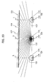
- FIG.20 shows an example of arrangement including an object-to-be-illuminated in a display employing LEDs as primary light source.
- display 121 is provided with a plurality of LED chips 125, light diffusion member 126 and object-to-be-illuminated (such as LCD-panel) 127.
- Each LED chip 125 is provided with LED 124.
- Light flux control member 123 provided with a hemisphere emission face 122 is fixed to a light emitting surface side of LED 124.
- Light from each LED chip is supplied to object-to-be-illuminated (such as LCD-panel) 127 after transmitting light diffusion member 126.
- object - to - be - illuminated 127 is illuminated two- dimensionally.
- FIG.21 illustrates another example of display employing a LED as primary light source.
- matrix- type display 130 is provided with display panel substrate 131, emission elements 132 arrayed thereon like matrix and lens case 133.
- Lens case 133 is located at a front side of emission elements 132, being mounted as to be in closely contact with display panel substrate 131.
- Hemisphere-like projection portions 134 are formed on lens case 133 as to correspond respectively to emission elements 124.
- Hollow 135 is formed within each projection portion 134 for accommodating emission element 132.
- Each hollow 135 has a side wall which is formed so refract and take in light from emission element 132 so that light thus taken in is directed to a front side (upward direction in FIG.21 ). Light from emission element 132 impinges only on an inner surface of hollow 135.
- Lens case 133 also has gap(s) 136 aground hollow(s) 135 accommodating emission element(s) 132. Light taken in lens case 133 after being emitted sideways from emission element(s) 132 is totally-reflected by slope(s) 137 of gap(s) 136, being directed to a frontal direction. As a result, matrix-type display 13 provide a frontal illumination of an increased brightness.
- Emission quantity varies rapidly at parts at which configuration of micro-lens arrays 102 is discontinuously changes and intermediate sections between LEDs 101 side by side are formed. This causes boundary areas between micro-lens arrays 102 to provide conspicuous emission brightness unevenness.
- Continuously arranged plural concave lenses 105 connected to each other are not employed. Further, continuously arranged plural convex lenses 106 connected to each other are not employed. Accordingly, it is difficult to illuminate a large area size object - to - be - illuminated uniformly in a backlighting arrangement.
- LED 108 Light from LED 108 is affected by converging lens 110 and diverging lens 111 successively. Such successive converging action and diverging action will decrease brightness unevenness as compared with surface light source device 100 (first prior art). However, light from LEDs 108 adjacent to each other is hardly mixed well. Therefore, if LEDs 108 adjacent to each other have emission colors, emission color unevenness between LEDs 108 adjacent to each other tends to be conspicuous.
- Brightness of frontal illumination light is large.
- light fluxes from lens cases 133 of emission elements 132 adjacent to each other tend to be hardly mixed together. This brings conspicuous unevenness in emission color.
- light H emitted from projection portion 134 of lens case 11133 and light H emitted after being totally reflected by slope 137 of gap 136 give a crossover at a location which would be seen easily by naked eyes. As a result, a ring-like locally bright portion can be generated. Such a ring-like locally bright portion would decrease illumination quality.
- the present invention can be applied to an emission device employing a mode according to which light of an emission element is emitted from a light flux control member, a surface light source device employing the mode in which one or more emission elements are adopted and a display using the surface light source device as an illumination means.
- An object of the present invention is to improve such emission device, surface light source device and display so that uniform two- dimensional illumination is realized and, if a back side area of a light flux control member can function as an incidence face, unevenness in emission color is avoided from being conspicuous.
- Another object of the present invention is to improve such emission device, surface light source device and display employing a single emission element as a light source (primary light source) so that light of the emission element can be diverged effectively, smoothly and broadly enough to reach a desired range.
- a single emission element as a light source (primary light source) so that light of the emission element can be diverged effectively, smoothly and broadly enough to reach a desired range.
- the present invention is applied to an emission device comprising at least one point-like-light-source and a light flux control member having a back face to which an output light flux of said point-like-light-source is incident and an emission face which is opposite to said back face and outputs illumination light forming a three- dimensional emission flux a travelling direction at a center of which is defined as reference optical axis.
- said emission face includes a light control emission face controlling emission of said illumination light
- said back face includes a first recess portion formed at location corresponding to said point-like-light-source and at least one second recess portion located in an area surrounding an opening-edge of said first recess portion, said second recess portion being configured as to be capable of restraining refraction on incidence of light of said point-like-light-source to said second recess portion from generating inner-propagation light having a travelling direction approaching said reference optical axis.
- said light control emission face is configured as to meets the following conditions (a), (b) and (c) regarding light emitted in a direction range which is at least within 75° from a maximum intensity light emission direction of said point-like-light-source, so far as out of a neighbour of said reference optical axis, under definition such that ⁇ 1 is angle of inner-propagation direction after incidence to said light flux control member with respect to a direction parallel with said reference optical axis and emission angle ⁇ 5 is angle of emission from said light control emission face with respect to a direction parallel with said reference optical axis,
- Said second recess portion may be a ring surrounding said first recess portion.
- said second recess portion may have a triangle-like cross section shape on a plane on which said reference optical axis extends and consists of a ring-like first slope adjacent to said first recess portion and a ring-like second slope which is located distantly from said first recess portion and provides a bridge connecting an end portion of said first slope with said back face.
- said first slope may be formed as to either extend on an extended part of straight line running between an emission center of said point-like-light-source and the other end portion of said first slope or be formed at a sharper angle as compared with inclination of said extended part of straight line so that light which has reached said second recess portion after being emitted from said point-like-light-source is not hindered from being incident to said second slope.
- said first slope may be formed as to be extend, in said cross section shape on said plane, on an extended part of strayed line running between an emission center of said point-like-light-source and said the other end portion of said first slope, and said second slope is formed as to be generally vertical with respect to said first slope.
- said at least one second recess portion may consist of a set of second recess portions, said set of second recess portions being arranged concentrically and successively as to surround said first recess portion, and all of said set of second recess portions except for one second recess portion that is located at the most inner side and is adjacent to said opening-edge of said first recess portion being configured as to be the same as or similar to said one second recess portion.
- said at least one second recess portion may consist of a set of second recess portions, said set of second recess portions being arranged concentrically and successively as to surround said first recess portion, and all of said set of second recess portions except for one second recess portion that is located at the most inner side and is adjacent to said opening- edge of said first recess portion being configured as to have first slope inclination gets gentler increasingly as compared with first slope inclination of said one second recess as distance of second recess portions from said first recess portion increases.
- said light control emission face may include a ring-like first emission face which is near to said reference optical axis and concentric with respect to said reference optical axis and a second emission face which is adjacent to and surrounds said first emission face, a connection part between said first emission face and said second emission face corresponding to a point of inflection of said light control emission face.
- said at least one point-like-light-source consists of a plurality of point-like-light-sources corresponding to each of which said first recess portion and said at least one second recess portion are formed on said back face of said light flux control member.
- the present invention is applied to a surface light source device comprising an emission device and a light diffusion member diffusing light outputted from said emission device.
- the surface light source device employs any of the above emission devices.
- the present invention is also applied to a display comprising a a surface light source device and an object- to- be- illuminated for displaying illuminated by light outputted from said surface light source device.
- the display employs the a
- a large part of light fluxes outputted from one or more point-like-light-sources enters into a light flux control member through a first recess portion(s) formed on a back face of the light flux control member, becoming inner-propagation light.
- Such inner-propagation light is emitted from a light control emission face of the light flux control member.
- some part of light fluxes outputted from one or more point-like-light-sources enters into the light flux control member through a second recess portion(s) formed on around the first recess portion(s). Refraction occurs on incidence to the second recess portion(s) as to restrain inner-propagation light travelling in directions nearing to directions parallel to the reference optical axis from being generated. Such an effect is owing to configuration of the second recess portion(s).
- inner- propagation generated by incidence to the second recess portion(s) is not emitted through the light control emission face, or, even if some light component is emitted through the light control emission face happens, it occurs only at a distal end portion of the light control emission face (only at an area very far from the reference optical axis).
- emission elements in cases of employing a plurality of emission elements as primary light sources, light from the respective emission elements can be mixed easily. This prevents illumination light emitted from the light flux control member from showing conspicuous illumination color unevenness even if unevenness in emission color exists among the emission elements. Besides, emission brightness is uniformalized and high quality illumination is obtained.
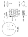
- FIGs.1 to 3 illustrate display 1 and surface light source device 2 employed therein, which are in accordance with the present invention.
- FIG.1 is a plan view of surface light source device 2, In other words, a plan view of display 1, with elements including a object - to - be - illuminated (such as LCD-panel) 3 being removed.
- FIG.2 is an outlined cross section view of display 1 along line X-X in FIG.1 .
- FIG.3 is a partially enlarged cross section view of display 1 shown in FIG.2 along a cross section including reference optical axis of emission element 4, giving an illustration of configuration of light control emission face 6 of light flux control member 5.
- reference optical axis L is defined as " light travelling direction at a center of a three- dimensional emission flux emitted from an emission device” .
- optical axis of emission element 4 is defined as " light travelling direction at a center of a three- dimensional emission flux emitted from emission element 4" . Described is on cases where optical axis of emission element 4 accords with reference optical axis L. Accordingly, reference optical axis L is expressed by “ optical axis L " hereafter.
- display 1 comprises a plurality of emission elements (point-like-light-sources such as LEDs) 4 as primary light source, light flux control member 5, plate-like light diffusion member 7 and object-to-be-illuminated 3.
- emission elements point-like-light-sources such as LEDs
- surface light source device 2 is constituted by emission elements 4, light flux control member 5, light diffusion member 7.
- Emission device 1 is constituted by emission elements 4 and light flux control member 5.
- Light diffusion member 7 has a rectangular plan shape, being provided with an emission face (front face) 8 and back face 12 as major faces. Emission elements 4 are disposed at generally constant intervals (at generally constant pitch) along back face side of light diffusion member 7 together with light flux control member 5. Object-to-be-illuminated 3 is disposed at front side of light diffusion member 7.
- Light flux control member 5 is configured as illustrated in FIGs.1 to 3 , being made of transparent resin material such as PMMA (polymethyl methacrylate), PC '(polycarbonate) or EP (epoxy resin), or transparent glass.
- light flux control member 5 has light control emission face 6 and generally ring-like flange portion 9, light control emission face 6 has a generally circular plan shape.
- Ring-like flange portion 9 is formed as to projects toward the outside of light control emission face 6.
- light control emission face 6 is formed as to project upward as compared with flange portion 9.
- emitting point 13 is defined as a point at which optical axis L and an upper face (emitting surface) 20 of emission element 4 cross.
- recess portions 14 are formed on the side of back face 12 of light flux control member 5 as first recess portions.
- each recess portion 14 is located as to correspond to each emission element 4.
- Recess portion 14 is configured like a hemisphere a center of which is emitting point 13, having radius of r 1 .
- a plurality of ring-like-recess-portions 15a to 15d are formed on the side of back face 12 as to surround concentrically and successively a periphery of recess portion 14.
- feet 17 are formed at constant intervals on the side of back face 12 along a periphery of the most outside ring-like recess portion 15 as to be located more distant from recess portion 14 as compared with ring-like recess portion 15.
- feet 17 are arranged on a circle concentric with the outermost ring-like recess portion 15d.
- Feet 17 are round-rod-like members which are utilized from mounting light flux control member 5 to substrate 16, with light flux control member 5 being positioned. Three feet 17 are engaged onto mounting holes 18 opened toward upper face 16a of substrate 16. Upper face 16a is opposite to light flux control member 5. Three mounting holes 18 are arranged at constant intervals on a circle center of which is emitting point 13. Light flux control member 5 can be secured as to be positioned with respect to emitting point 13 of emission element 4 by causing feet 17 to be engaged into mounting holes 18. It is noted that both a center of light flux control member 5 and emitting point 13 are located on optical axis L.
- Gap ⁇ is generated between light emitting face 20 of emission element 4 and back face 12 of light flux control member 5 by mounting light flux control member 5 to substrate 16. Such gap ⁇ can be brought by mounting error which involved by a process such that light flux control member 5 is mounted to substrate 16 as to cause emission element 4 to be accommodated into recess portion 14. Gap ⁇ may be formed in order to promote diffusion of heat generated by emission element 4.
- each foot 17 is fat at a root side thereof and thin at a topside 6thereof, providing a fat portion near to a root of foot 17 and a thin portion near to a top of foot 17.
- Each mounting hole 18 has a diameter that does not allow a fat portion of foot 17 to pass and allows a thin portion of foot 17 to pass, being formed as to penetrate substrate 16.
- Thin portions of feet 17 are pushed into mounting holes 18 so that top portions of feet 17 reach lower face 16b of substrate 16 and extrude therefrom. Then the top portions are heat-deposited to position light flux control member 5 with respect to substrate 16. It is noted that “ close-fit " may be applied to fitting of feet 17 into mounting holes 18 or adhesive may be applied to fixing of feet 17 to mounting holes 18 if the device is used under circumstance tending to cause light flux control member 5 to fall away from substrate 16.
- Light control emission face 6 of light flux control member 5 consists of first emission face 6a and second emission face 6b.
- First emission face 6a occupies a predetermined area through a center of which optical axis L extends.
- Second emission face 6b is formed around first emission face 6a as to be continuously connected to first emission face 6a.
- first emission face 6a has a curved surface sinking downward smoothly, namely, a downward- convex smooth curve, providing a recess shape like a shape which is obtained by cutting out and picking up a part of sphere.
- second emission face 6b has a smoothly curved upward-convex surface which is adjacent to firs emission face 6a. As shown in FIG.4a , second emission face 6b has a ring-like plan shape surrounding first emission face 6a. First emission face 6a and second emission face 6b are connected smoothly to each other, providing a connection portion corresponding to point of inflection Po. In other words, point of inflection Po is located at boundary portion between first emission face 6a and second emission face 6b.
- a curve showing profile of first emission face 6a and another curve showing profile of second emission face 6b meet at point Po and are connected there to each other.
- point Po is an inflection point of a continuous curve giving a cross section profile (surface configuration) of light control emission face 6.
- third emission face 6c is formed at periphery side of second emission face 6b as to provide a bridging portion between second emission face 6b and flange portion 9. It is noted that a generally straightly inclined slope forming third emission face 6c shown in FIG.4b is merely an example. Third emission face 6c may be formed of a curved slope unless the curved slope is configured as to disturb broad and uniform emission from light flux control member 5.
- inner-propagation light means light which propagates within light flux control member 5 after being emitted from emission element 4 and then entering into light flux control member5.
- maximum intensity direction " maximum intensity primary light” , “ maximum intensity “ .”
- half-intensity primary light and “ half-intensity angle” are defined as follows in connection with angular characteristics of light intensity.
- the present invention is described under provision such that maximum intensity direction substantially accords with direction of optical axis L (normal direction of reference plane C). Usually, such provision is practical and maximum intensity direction can be regarded as the same direction as the direction of optical axis L.
- emission direction intensity profile (angular characteristics) of emission element 4 is substantially symmetric with respect to optical axis L and a unique half- intensity angle (absolute value) exists.
- configuration of curved surface of light control emission face 6 shown in FIG.3 meets the following conditions.
- configuration of curved surface of light control emission face 6 is formed as to satisfy the conditions.
- ⁇ is a small angle expressing being near angularly to a direction of optical axis L.
- a preferable value of ⁇ is 5 degrees that defines an angle range of ⁇ 1 within ⁇ 5 degrees.
- FIG.6 gives a graphic illustration showing a relation between angle ⁇ 1 and angle ⁇ 5 ( 3 emission angle from light flux control member 5).
- curve 21 gives an example meeting the above conditions.
- the above-mentioned " predetermined angle larger than half-intensity angle" is ⁇ 1 .
- ⁇ is defined as coefficient expressing degree of light diffusion performed by light flux control member 5.
- Angles ⁇ 5 and ⁇ 3 are given by the following formula (1) and formula (2), respectively, under condition of ⁇ 1 ⁇ ⁇ 1 .
- ⁇ ⁇ 5 1 + ⁇ ⁇ 1 - ⁇ ⁇ 1 ⁇ ⁇ / ⁇ ⁇ 1 ⁇ ⁇ ⁇ 1
- ⁇ ⁇ 1 absolute value ⁇ ⁇ ⁇ 1 ⁇ ⁇ 3 tan - 1 ⁇ sin ⁇ ⁇ 5 - n ⁇ sin ⁇ ⁇ 1 / cos ⁇ ⁇ 5 - n ⁇ cos ⁇ ⁇ 1 ⁇
- n refractive index of light flux control member
- ⁇ 3 is expressed as to be regarded as a function of ⁇ 1 .
- FIG.7 gives a graph showing an example of this function.
- curve 23 expresses a relation between ⁇ 3 and ⁇ 1 determined on the basis of above formulae (1) and (2). Curve 23 teaches the followings.
- ring-like recesses 15 formed on back face 12 of light flux control member 5 are composed of first ring-like recess 15a and second to fifth ring-like recesses 15b to 15d.
- First ring-like recess 15a is formed as to be adjacent to recess portion 14.
- Second to fifth ring-like recesses 15b to 15d are formed as to successively located in order from inside to outside radially.
- first ring-like recess 15a has a triangle-like cross section along a plane including optical axis L. It is noted that the plane including optical axis L is vertical to back face 12 of light flux control member.
- First ring-like recess 15a consists of ring-like first slope 15a1 and ring-like second slope 15a2.
- First slope 15a1 is generally located on an extended part of straight line 25 running from emitting point 13 to opening edge 24 of recess portion 14.
- Second slope 15a2 provides a bridge connecting end portion 15a3 of first slope 15a1 to a side of back face 12. End portion 15a3 is an end portion other than opening edge 24 and located at w in depth from back face 12. Second slope 15a2 is generally vertical to first slope 15a1.
- First slope 15a1 is generally located on an extended part of straight line 25 running from emitting point 13 to opening edge 24 of recess portion 14 " means either (I) or (II) below.
- First slope 15a1 is preferably inclined as to hardly receive light which is directly directed to back face 12 after being emitted from emission element 4.
- Second slope 15a2 is generally vertical to first slope 15a1 " is related to the illustration of FIG.4c , meaning that second slope 15a2 crosses first slope 15a1 at an angle slightly greater or smaller than 90 ° under consideration of manufacturing error.
- Second slope 15a2 is preferably inclined as to restrain light of emission element 4 from being refracted on being incident thereto toward a direction which comes nearer to reference optical axis L as compared with light travelling direction before being incident.
- second ring - like recess portion 15b has a triangle- like cross section different from said triangle-like cross section of first ring - like recess portion 15a, consisting of ring-like first slope 15b1 and ring-like second slope 15b2.
- First slope 15b1 is generally located on an extended part of straight line 27 running from emitting point 13 to back face side end edge 26 of second slope 15a2 of first ring - like recess portion 15a.
- Second slope 15b2 provides a bridge connecting end portion 15b3 of slope 15b1 to a side of back face 12. End portion 15b3 is an end portion other than back face side end edge 26 and located at w in depth from back face 12. Second slope 15b2 is generally vertical to first slope 15b1.
- third ring - like recess portion 15c has a triangle-like cross section different from both triangle- like cross sections of first and second ring - like recess portions 15a, 15b, consisting of ring-like first slope 15c1 and ring-like second slope 15c2.
- First slope 15c1 is generally located on an extended part of straight line 30 running from emitting point 13 to back face side end edge 28 of second slope 15b2 of second ring - like recess portion 15b.
- Second slope 15c2 provides a bridge connecting end portion 15c3 of slope 15c1 to a side of back face 12. End portion 15c3 is an end portion other than back face side end edge 28 and located at w in depth from back face 12. Third slope 15c2 is generally vertical to first slope 15c1.
- forth ring - like recess portion 15d has a triangle-like cross section different from every triangle-like cross section of first to third ring - like recess portions 15a to 15c, consisting of ring-like first slope 15d1 and ring-like second slope 15d2.
- First slope 15d1 is generally located on an extended part of straight line 32 running from emitting point 13 to back face side end edge 31 of second slope 15c2 of third ring - like recess portion 15c.
- Second slope 15d2 provides a bridge connecting end portion 15d3 of slope 15d1 to a side of back face 12.
- End portion 15d3 is an end portion other than back face side end edge 31 and located at w in depth from back face 12.
- Second slope 15d2 is generally vertical to first slope 15d1.
- depth w of first to forth ring - like recess portions 15a to 15d and distance L2 from optical axis L to the outermost edge (back face side end edge 33 of second slope 15d2) are preferably determined under consideration of factors such as size of light flux control member 5, emission brightness of emission element 4, gap distance ⁇ from emitting surface 20 of emission element 4 to back face 12 of light flux control member 5 and half-intensity angle of emission element 4,
- ring - like recess portions 15 formed on back face 12of light flux control member 5 as second recess portions in the embodiment work effectively under situation such that emission element 4 emits light including rays which are largely inclined light with respect to optical axis L and incident to back face 12.
- gap distance ⁇ is preferably small so that a great part of the light emitted from emission element 4 is incident to first recess portion 14 and the other part of the light emitted from emission element 4 is incident to second recess portions 15.
- gap distance ⁇ is preferably formed as to be smaller than radius of opening edge 24 of first recess portion 14.
- first recess portion 14 As shown in FIG.2 . Incidence to first recess portion 14 involves substantially no refraction in the embodiment. The other is incident to second ring - like recess portions 15a to 15d, entering into light flux control member 5.
- second slopes 15a2, 15b2, 15c2 and 15d2 hardly involves refraction because they provide surfaces generally vertical to travelling direction of light H emitted from emission element 4. As a result, generation of rays deflected as to come near to optical axis L.
- light H from emission element 4 is emitted from light control emission face 6 to the outside (air) according to Snell's Law after inner - propagation.
- Light emitted from light control emission face 6 is directed to smoothly expanded broad angles uniformly without locally strong emitting directions such as direction corresponding to optical axis L.
- Such performance is superior to that of prior art shown in FIG.20 in which hemisphere-like light flux control member 123 is employed.
- back face 12 of light flux control member 5 lacks second recess portions 15 shown in FIG.4 , namely, flat back face 12 parallel to reference plane C is formed as shown in FIGs.8 , light H from emission element is refracted as to come near to optical axis L.
- Such phenomenon occurs, in other words, when light flux control member 5 shown in FIG.8 is employed.
- Such light gathering part 35 provide a ring - like locally bright part brighter than the other part.
- Such ring - like bright part is seen from above emission face 36 of light diffusion member 7, resulting in a reduced illumination quality.
- Light flux control member 5 of the embodiment in accordance with the present invention can avoid such a ring - like locally bright portion from appearing because second recess portions 15 function as to restrains refraction on entering into light flux control member 5 from producing rays which bring ring - like locally bright part.
- light diffusion member 7 is a sheet-like or flat plate-like optical element capable of transmitting and diffusing light.
- Base material of light flux control member 7 is, for example, light permeable resin such as PMMA (polymethyl methacrylate) or PC '(polycarbonate).
- Light diffusion member 7 has a plan size generally the same as that of object - to - be - illuminated such as LCD-panel, advertising panel or other display panels.
- Light diffusion member 7 is provided with light diffusion ability given to at least inside or surface.
- light diffusion member 7 has a surface provided with micro- unevenness such as prismatic projections, emboss-processed surface, bead-coating surface. Micro-particles may be dispersed in light diffusion member 7 so that inside scattering ability is given.
- Light diffusion member 7 may be mounted on an inner side of object-to-be-illuminated 3 or, alternatively, may be disposed as to separated from object-to-be-illuminated 3 between object-to-be-illuminated 3 and light flux control member 5.
- emission device 1 using light flux control member 5 and surface light source device including emission device 1 by referring to FIGs.1 to 4c .
- first and second emission faces 6a, 6b may be determined under consideration of various factors as follows.
- Third emission face 6c is formed as to have a configuration that is obtained by rotating tangential line at the outermost of second emission face 6b around optical axis L by 360 degrees.
- a range of ⁇ 1 ⁇ ⁇ 2 gives (corresponds to) a range of first emission face 6a.
- a range of ⁇ 2 ⁇ ⁇ 1 ⁇ ⁇ 1 gives (corresponds to) a range of second emission face 6b.
- a range of ⁇ 1 ⁇ ⁇ 1 gives (corresponds to) a range of third emission face 6c.
- ring-like recesses 15 of light flux control member 5 composed of first to forth ring-like recesses 15a to 15d, being expressed by the following data.
- first to forth ring-like recess portions 15a to 15d are have second slopes 15a2 to 15d2 which are generally vertical to first slopes 15a1 to 15d1, respectively.
- the simulation was performed for studying a preferable range in which ring-like recess portions are formed to prevent ring-like locally bright part from appearing due to incidence to back face 12 of light flux control member 5.
- First prepared was a surface light source device including an emission device which are the same as surface light source device 2 and emission device 1 in accordance with embodiment except that no ring-like recess portion 15 is formed on a back face.
- prepared light flux control member 5 having no ring-like recess portion 15 on the back face thereof is called “ dummy light flux control member 5 " .
- the larger area of opening 38 is the larger is illuminance of ring- like locally bright part until incidence angle ⁇ 1 in FIG.9 reaches about 78 degrees. However, if incidence angle ⁇ 1 exceeds about 78 degrees, illuminance converges to a generally constant value gradually.
- ring- like locally bright part 35 appears as to surround optical axis L on surface-to-be-illuminated 34 of light diffusion member 7. Such ring-like locally bright part 35 reduces illumination quality.
- light flux control member 5 in accordance with the embodiment prevent light incident to a part other than recess portion 14 from being refracted as to come nearer to optical axis 1.
- any ring-like locally bright part hardly appear on surface-to-be-illuminated 34 of light diffusion member 7, being free from reduction in illumination quality.
- FIG.11 is a graphic diagram illustrating an emission quantity distribution of light supplied to object - to - be - illuminated 3 of display 1. Shown in FIG.11 is an emission quantity distribution of emission at locations along line X3-X3 in FIG.1 on emission face 8 of light diffusion member 7 (See FIG.2 ). In FIG-11. ordinate gives illuminance (1x) and abscissa gives distance from a center of surface light source device 2 shown in FIG.2 along line X3-X3.
- line S1 gives an illuminance distribution of surface light source device 2 employing emission device 1 in accordance with the embodiment.
- line S2 gives an illuminance distribution of surface light source device 2 employing emission device 1 shown in FIG.8 .
- line S3 gives an illuminance distribution of surface light source device 2 employing no light flux control member. In other words, line S3 corresponds to a case of direct irradiation from emission element 4 to light diffusion member 7 is applied.
- line S3 gives an extremely high illuminance just above emission element 4 and a relatively low illuminance at sections corresponding to absence of emission element 4. In other words, illuminance varies largely, failing to provide uniform illumination.
- Line S2 gives an improved illuminance distribution as compared with S2. In other words, uniformalized illumination to an extent is achieved.
- some rays (light H) are refracted as to come near to optical axis L on incidence to back face 12 of light flux control member 5. These rays cross over with other rays coming from recess portion 14. This brings ring-like locally bright part 35 at a center of section corresponding to absence of emission element 4. Such ring-like locally bright part 35 is viewed through light diffusion member m 7, being harmful.
- line S1 gives an illuminance distribution such that no ring-like locally bright part 35 appears. This brings a very uniform illumination.
- a greater part of the light emitted from emission element 4 enters into light flux control member 5 via recess portion 14, being emitted from light control emission face 6.
- the other part of the light emitted from emission element 4 enters into light flux control member 5 via ring-like recess portions 15 (15a to 15d), becoming inner- propagation light which is not deflected as to come nearer to optical axis L by refraction on incidence to ring-like recess portions 15.
- light H via ring-like recess portions 15 is not emitted from light control emission face 6, or, if some emission involved, it occurs in the vicinity of the outermost periphery of light control emission face 6. This prevents ring- like locally bright part from appearing, with the result that illumination light is kept high.
- Emission from light control emission face 6 is broadly and smoothly diverged, providing a uniform illumination.
- emission elements 4 are arranged at intervals as primary light source, light fluxes from respective emission elements 4 are mixed mutually with ease. Accordingly, if unevenness in emission color exists among emission elements 4, light emitted from light flux control member 5 hardly shows unevenness in illumination color.
- back face 12 of light flux control member 5 is distant from emission element 4 by a predetermined distance ⁇ as to enable heat generated by emission element 4 to be radiated well, bad influence by heat is avoided.
- FIGs.12a, 12b and 13 illustrate light flux control member 5 employ ed in a first modification of the present invention. It is noted that light flux control members 5 employed in the first modification and in second to third modifications described later are structured in the same way as light flux control member 5 employed in the embodiment already described except for recess portion(s) 15. Therefore common reference numerals are used for common elements and repeated description is omitted.
- light flux control member 5 has back face 12 provided with recess portions 15 consisting of first to eighth recess portions 15a to 15h.
- second to eighth ring-like recess portions 15b to 15h are formed as to be structured in the same way,
- Such light flux control member 5 gives a functional feature to emission device 1 employing the same as follows.
- incident light H of a large incidence angle (about half- intensity angle) to light flux control member 5 is slightly deflected by refraction as to come near to optical axis 1, then being emitted from light flux control member to be supplied to light diffusion member 7. This will bring crossing over with light H coming from recess portion 14, producing a ring-like locally bright part on surface-to-be-illuminated 34 of light diffusion member 7.
- the above ring-like locally bright part has a very large size and the above deflected light has a weak intensity (brightness). Therefore such a large and weak ring-like locally bright part is not conspicuous, being hardly harmful.
- the first modification can has similar advantages as compared with the embodiment previously described.
- FIGs.14a, 14b and 15 illustrate light flux control member 5 employ ed in a second modification of the present invention.
- light flux control member 5 has back face 12 provided with a single ring-like recess portion 15.
- Ring-like recess portion 15 has a triangle-like cross section, provided with ring-like first slope 15a1 and ring-like second slope 15a2.
- First slope 15a1 is generally located on an extended part of straight line 25 running from emitting point 13 to opening edge 24 of recess portion 14. Ring like second slope 15a2 providing a bridge portion connecting end portion 15a3 to a side of back face 12, being generally vertical to first slope 15a1.
- Ring-like recess portion 15 has a configuration corresponding to a configuration obtained by enlarging first ring-like recess portion 15a of light flux control member 5 employed in the first modification.
- the second modification is obtained by substitute first to eighth ring- like recess portions 15a to 15h in the first modification with one ring-like recess portion 15.
- incident light H of a large incidence angle (about half- intensity angle) to light flux control member 5 is slightly deflected by refraction as to come near to optical axis 1, then being emitted from light flux control member to be supplied to light diffusion member 7. This will bring crossing over with light H coming from recess portion 14, producing a ring-like locally bright part on surface-to-be-illuminated 34 of light diffusion member 7.
- the above ring-like locally bright part has a very large size and the above deflected light has a weak intensity (brightness).
- a large and weak ring-like locally bright part is not conspicuous, being hardly harmful.
- FIG.16 illustrates light flux control member 5 employed in a third modification.
- light flux control member 5 has back face 12 provided with a plurality of ring-like recess portions 15a to 15d which are arranged in order successively toward outside at a constant pitch L5 from recess portion 14.
- Ring-like recess portion 15d has second slope 15d2, being formed so that back face side end edge 45 of second slope 15d2 is located at generally the same position as the position of back face side end edge 33 of second slope 15d2 of forth ring-like recess portion 15d in the embodiment described above.
- the outermost ring- like recess portion is ring-like recess portion 15d.
- ring-like recess portions 15 can prevent ring-like locally bright parts from appearing because refraction on incidence to ring-like recess portions 15 hardly involve generation of rays deflected as ro come near to optical axis L.
- the third modification can has similar advantages as compared with the embodiment previously described.
- Such a conspicuous ring-like locally bright part can be generated by light coming from recess portion 14 enters into first slope 15a1 before reaching light control emission face 6 due to total reflection.
- second recess portion is small enough, only slight inner-incidence to first slope 15a1 occurs, resulting in being free from conspicuous ring- like locally bright part appearance.
Landscapes
- Physics & Mathematics (AREA)
- General Physics & Mathematics (AREA)
- Optics & Photonics (AREA)
- Nonlinear Science (AREA)
- Mathematical Physics (AREA)
- Chemical & Material Sciences (AREA)
- Crystallography & Structural Chemistry (AREA)
- Engineering & Computer Science (AREA)
- General Engineering & Computer Science (AREA)
- Planar Illumination Modules (AREA)
- Liquid Crystal (AREA)
- Illuminated Signs And Luminous Advertising (AREA)
Applications Claiming Priority (1)
| Application Number | Priority Date | Filing Date | Title |
|---|---|---|---|
| JP2007289732A JP5077942B2 (ja) | 2007-11-07 | 2007-11-07 | 発光装置、面光源装置、及び表示装置 |
Publications (3)
| Publication Number | Publication Date |
|---|---|
| EP2058679A2 true EP2058679A2 (fr) | 2009-05-13 |
| EP2058679A3 EP2058679A3 (fr) | 2011-11-23 |
| EP2058679B1 EP2058679B1 (fr) | 2014-05-28 |
Family
ID=40380067
Family Applications (1)
| Application Number | Title | Priority Date | Filing Date |
|---|---|---|---|
| EP08168091.0A Not-in-force EP2058679B1 (fr) | 2007-11-07 | 2008-10-31 | Dispositif d'émission, dispositif de source lumineuse de surface et affichage |
Country Status (4)
| Country | Link |
|---|---|
| US (1) | US8251547B2 (fr) |
| EP (1) | EP2058679B1 (fr) |
| JP (1) | JP5077942B2 (fr) |
| CN (1) | CN101430063B (fr) |
Cited By (8)
| Publication number | Priority date | Publication date | Assignee | Title |
|---|---|---|---|---|
| EP2098905A1 (fr) | 2008-03-05 | 2009-09-09 | Enplas Corporation | Dispositif d'émission, dispositif de source lumineuse de surface et affichage |
| EP2287653A1 (fr) * | 2009-08-20 | 2011-02-23 | Panasonic Electric Works Co., Ltd | Lentille optique et accessoire d'éclairage l'utilisant |
| EP2330453A1 (fr) * | 2009-11-19 | 2011-06-08 | LG Innotek Co., Ltd. | Lentille et appareil électroluminescent doté de celle-ci |
| EP2434199A1 (fr) * | 2009-06-30 | 2012-03-28 | Sharp Kabushiki Kaisha | Dispositif d éclairage, appareil d affichage et équipement de réception de télévision |
| EP2458656A3 (fr) * | 2009-10-15 | 2013-01-16 | LG Innotek Co., Ltd. | Appareil électroluminescent |
| US8395183B2 (en) | 2009-11-20 | 2013-03-12 | Lg Innotek Co., Ltd. | Light emitting apparatus |
| EP2426521A3 (fr) * | 2010-09-06 | 2014-05-07 | Samsung Electronics Co., Ltd. | Lentille optique et module de source lumineuse et lampadaire en disposant |
| EP2840307A1 (fr) * | 2013-08-20 | 2015-02-25 | Funai Electric Co., Ltd. | Dispositif d'éclairage et dispositif d'affichage |
Families Citing this family (57)
| Publication number | Priority date | Publication date | Assignee | Title |
|---|---|---|---|---|
| KR100990640B1 (ko) * | 2008-05-29 | 2010-10-29 | 삼성엘이디 주식회사 | 확산렌즈 및 확산렌즈를 이용한 발광소자 조립체 |
| WO2010146904A1 (fr) * | 2009-06-15 | 2010-12-23 | シャープ株式会社 | Module electroluminescent, dispositif d'eclairage, dispositif d'affichage, et recepteur de television |
| CN102803826A (zh) * | 2009-06-30 | 2012-11-28 | 夏普株式会社 | 照明装置、显示装置以及电视接收装置 |
| JP2011023204A (ja) * | 2009-07-15 | 2011-02-03 | Sharp Corp | 発光装置、光束制御部材および当該発光装置を備える照明装置 |
| JP5719104B2 (ja) * | 2009-08-24 | 2015-05-13 | 株式会社エンプラス | 光束制御部材、発光装置、面光源装置、及び表示装置 |
| US8827478B2 (en) | 2009-11-06 | 2014-09-09 | Sharp Kabushiki Kaisha | Lighting device, display device, and television receiver |
| WO2011062089A1 (fr) | 2009-11-17 | 2011-05-26 | シャープ株式会社 | Unité d'émission de lumière de surface et dispositif d'affichage équipé d'une telle unité |
| EP2516921B1 (fr) * | 2009-12-21 | 2018-11-28 | Harman Professional Denmark ApS | Collecteur de lumière à lentilles centrale et périphérique complémentaires asymétriques en rotation |
| TWI561770B (en) * | 2010-04-30 | 2016-12-11 | Samsung Electronics Co Ltd | Light emitting device package, light source module, backlight unit, display apparatus, television set, and illumination apparatus |
| CN102261619A (zh) * | 2010-05-25 | 2011-11-30 | 神讯电脑(昆山)有限公司 | 透光板改良结构 |
| US20130070168A1 (en) * | 2010-05-26 | 2013-03-21 | Sharp Kabushiki Kaisha | Led light source, led backlight, liquid crystal display device and tv reception device |
| KR20120050179A (ko) | 2010-11-10 | 2012-05-18 | 삼성엘이디 주식회사 | 플래시 렌즈 및 이를 채용한 플래시 모듈 |
| KR101109581B1 (ko) * | 2010-12-01 | 2012-01-31 | 노명재 | 엘이디 광확산용 확장형 아이시클타입 광 조정렌즈 |
| JP2012195165A (ja) * | 2011-03-16 | 2012-10-11 | Toshiba Corp | 導光板、光源装置及び表示装置 |
| JP2014518437A (ja) * | 2011-06-28 | 2014-07-28 | フレクストロニクス オートモーティブ ゲゼルシャフト ミット ベシュレンクテル ハフツング ウント コンパニー コマンディートゲゼルシャフト | Ledランプ |
| CN102252267A (zh) * | 2011-07-26 | 2011-11-23 | 青岛海信电器股份有限公司 | 透镜、led光源装置和led背光模组 |
| TWI377709B (en) | 2011-10-18 | 2012-11-21 | E Pin Optical Industry Co Ltd | Led lens and light source device using the same |
| JP6209527B2 (ja) * | 2011-12-02 | 2017-10-04 | ソウル セミコンダクター カンパニー リミテッド | 発光モジュール及びレンズ |
| US10047930B2 (en) * | 2011-12-02 | 2018-08-14 | Seoul Semiconductor Co., Ltd. | Light emitting module and lens |
| JP5641547B2 (ja) * | 2012-04-10 | 2014-12-17 | マイクロコントロールシステムズ株式会社 | 配光分散制御型led照明装置及び該装置を用いた照明方法 |
| CN102705777B (zh) * | 2012-06-29 | 2015-05-20 | 冠捷显示科技(厦门)有限公司 | 底面为曲面结构的二次透镜 |
| JP6046398B2 (ja) * | 2012-07-04 | 2016-12-14 | 株式会社エンプラス | 面光源装置および表示装置 |
| CN103574319A (zh) * | 2012-07-25 | 2014-02-12 | 欧司朗股份有限公司 | 制造照明装置的方法和由该方法制成的照明装置 |
| CN103574514A (zh) * | 2012-08-03 | 2014-02-12 | 鸿富锦精密工业(深圳)有限公司 | Led导光元件、led光源模块及直下式led电视 |
| CN104583668B (zh) | 2012-08-22 | 2020-04-03 | 首尔半导体株式会社 | Led背光源的照明透镜、发光设备、表面光源设备、显示设备 |
| US10503010B2 (en) | 2012-08-22 | 2019-12-10 | Seoul Semiconductor Co., Ltd. | Thin direct-view LED backlights |
| JP6111110B2 (ja) * | 2012-08-27 | 2017-04-05 | 株式会社エンプラス | 光束制御部材、発光装置、面光源装置および表示装置 |
| CN103672475B (zh) | 2012-09-20 | 2017-10-24 | 欧司朗股份有限公司 | 照明装置及其制造方法 |
| JP6119166B2 (ja) * | 2012-09-28 | 2017-04-26 | 岩崎電気株式会社 | 発光素子ユニット及び照明器具 |
| JP5957364B2 (ja) * | 2012-10-25 | 2016-07-27 | 株式会社エンプラス | 光束制御部材、発光装置、面光源装置および表示装置 |
| TW201422984A (zh) * | 2012-12-11 | 2014-06-16 | 鴻海精密工業股份有限公司 | 光學透鏡以及應用該光學透鏡的發光元件 |
| CN103062705B (zh) * | 2012-12-19 | 2015-04-08 | 冠捷显示科技(厦门)有限公司 | 大角度扩散的光学透镜 |
| TWI574049B (zh) * | 2012-12-26 | 2017-03-11 | 鴻海精密工業股份有限公司 | 透鏡及使用該透鏡的背光模組 |
| WO2014102341A1 (fr) * | 2012-12-31 | 2014-07-03 | Iee International Electronics & Engineering S.A. | Système optique générant un champ lumineux structuré à partir d'un réseau de sources lumineuses au moyen d'un élément réfractif ou réfléchissant de structuration de la lumière |
| JP6102022B2 (ja) * | 2013-02-22 | 2017-03-29 | パナソニックIpマネジメント株式会社 | Ledモジュール及び照明器具 |
| US10355182B2 (en) * | 2013-03-13 | 2019-07-16 | Lumileds Llc | Encapsulated LED lens with bottom reflectors |
| CN103148419B (zh) * | 2013-03-28 | 2015-08-12 | 应春斌 | Led格栅灯具 |
| TW201512596A (zh) * | 2013-09-18 | 2015-04-01 | 鴻海精密工業股份有限公司 | 透鏡及使用該透鏡之光源模組 |
| TWI589964B (zh) * | 2013-12-26 | 2017-07-01 | 鴻海精密工業股份有限公司 | 發光裝置及背光模組 |
| JP6310285B2 (ja) * | 2014-03-18 | 2018-04-11 | 株式会社エンプラス | 発光装置、面光源装置および表示装置 |
| JP6356997B2 (ja) * | 2014-04-02 | 2018-07-11 | 株式会社エンプラス | 光束制御部材、発光装置、面光源装置および表示装置 |
| KR20160015447A (ko) * | 2014-07-30 | 2016-02-15 | 삼성전자주식회사 | 발광소자 패키지용 렌즈, 광원 모듈, 조명 장치 및 조명 시스템 |
| JP5903481B2 (ja) * | 2014-11-19 | 2016-04-13 | 株式会社エンプラス | 発光装置、面光源装置、及び表示装置 |
| JP2017017001A (ja) * | 2015-07-01 | 2017-01-19 | 株式会社エンプラス | 光束制御部材、発光装置、面光源装置および表示装置 |
| WO2017002686A1 (fr) * | 2015-07-01 | 2017-01-05 | 株式会社エンプラス | Élément de régulation de flux lumineux, dispositif d'émission de lumière, dispositif source de lumière de surface et dispositif d'affichage |
| JP6682229B2 (ja) * | 2015-09-03 | 2020-04-15 | 株式会社エンプラス | 光束制御部材、発光装置、面光源装置および表示装置 |
| JP6660690B2 (ja) * | 2015-09-04 | 2020-03-11 | 株式会社エンプラス | 光束制御部材、発光装置および面光源装置 |
| TWI621811B (zh) * | 2015-09-15 | 2018-04-21 | 鴻海精密工業股份有限公司 | 非球面光學鏡片及其所構成的發光裝置 |
| KR101935019B1 (ko) | 2015-11-26 | 2019-01-03 | 몰렉스 엘엘씨 | 확산 렌즈 및 이를 포함하는 발광 모듈 |
| CN105549202B (zh) * | 2015-12-08 | 2018-06-08 | 江南大学 | 用于led扩展光源的自由曲面准直器的设计方法 |
| JP6705174B2 (ja) * | 2016-01-08 | 2020-06-03 | 三菱電機株式会社 | 光源装置および照明装置 |
| JP6629601B2 (ja) * | 2016-01-21 | 2020-01-15 | 株式会社エンプラス | 光束制御部材、発光装置、面光源装置および表示装置 |
| CN106090826B (zh) * | 2016-06-07 | 2019-09-20 | 广州创维平面显示科技有限公司 | 光学透镜和发光装置 |
| JP2018125245A (ja) * | 2017-02-03 | 2018-08-09 | 株式会社エンプラス | 面光源装置および表示装置 |
| WO2018159977A1 (fr) * | 2017-02-28 | 2018-09-07 | 서울반도체주식회사 | Dispositif d'affichage, unité de rétroéclairage, module électroluminescent et lentille |
| JP2018181726A (ja) * | 2017-04-19 | 2018-11-15 | 株式会社エンプラス | 光束制御部材、発光装置、面光源装置および表示装置 |
| TWI671491B (zh) * | 2019-03-06 | 2019-09-11 | 友達光電股份有限公司 | 背光源組件以及背光模組 |
Citations (6)
| Publication number | Priority date | Publication date | Assignee | Title |
|---|---|---|---|---|
| JPS59226381A (ja) | 1983-06-08 | 1984-12-19 | 株式会社東芝 | 発光表示装置 |
| JPS636702A (ja) | 1986-06-27 | 1988-01-12 | 株式会社小糸製作所 | 照明装置 |
| JP2001025098A (ja) | 1999-07-06 | 2001-01-26 | Matsushita Electric Ind Co Ltd | 車載用音響システム |
| JP2002049326A (ja) | 2000-08-02 | 2002-02-15 | Fuji Photo Film Co Ltd | 平面光源およびそれを用いた表示素子 |
| EP1641052A2 (fr) | 2004-09-27 | 2006-03-29 | Enplas Corporation | Dispositif émetteur, source lumineuse de surface, panneau d'affichage et dispositif de contrôle du flux lumineux |
| EP2023038A2 (fr) | 2007-08-09 | 2009-02-11 | Sharp Kabushiki Kaisha | Lentille de diffusion pour retro-éclairage de LCD par LED. |
Family Cites Families (11)
| Publication number | Priority date | Publication date | Assignee | Title |
|---|---|---|---|---|
| US5404869A (en) * | 1992-04-16 | 1995-04-11 | Tir Technologies, Inc. | Faceted totally internally reflecting lens with individually curved faces on facets |
| DE69803297T2 (de) * | 1997-08-12 | 2002-08-22 | Breault Res Organization Inc | Doppelreflektierende linse |
| ES2157846B1 (es) * | 1999-12-02 | 2002-03-01 | Univ Madrid Politecnica | Dispositivo con lente discontinua de reflexion total interna y dioptrico asferico para concentracion o colimacion de energia radiante. |
| JP4091233B2 (ja) | 2000-03-03 | 2008-05-28 | ローム株式会社 | ドットマトリクス表示装置 |
| JP4212902B2 (ja) * | 2003-01-07 | 2009-01-21 | 大日本印刷株式会社 | フレネルレンズ、フレネルレンズ成形型、フレネルレンズ製造方法及びフレネルレンズを用いた透過型スクリーン |
| JP4441854B2 (ja) * | 2003-11-25 | 2010-03-31 | オムロン株式会社 | 面光源装置及び当該装置を用いた機器 |
| DE102005020908A1 (de) | 2005-02-28 | 2006-08-31 | Osram Opto Semiconductors Gmbh | Beleuchtungsvorrichtung |
| JP2007141113A (ja) | 2005-11-22 | 2007-06-07 | Dainippon Printing Co Ltd | バイオメトリクス認証機能を備えたicカード、および、icカードプログラム |
| JP4863357B2 (ja) * | 2006-01-24 | 2012-01-25 | 株式会社エンプラス | 発光装置、面光源装置、表示装置及び光束制御部材 |
| JP5060059B2 (ja) * | 2006-03-10 | 2012-10-31 | パナソニック株式会社 | 光学部品及びそれを用いた照明装置 |
| JP4628302B2 (ja) | 2006-04-24 | 2011-02-09 | 株式会社エンプラス | 照明装置及び照明装置のレンズ |
-
2007
- 2007-11-07 JP JP2007289732A patent/JP5077942B2/ja active Active
-
2008
- 2008-10-31 EP EP08168091.0A patent/EP2058679B1/fr not_active Not-in-force
- 2008-11-04 US US12/289,797 patent/US8251547B2/en not_active Expired - Fee Related
- 2008-11-05 CN CN200810172874XA patent/CN101430063B/zh not_active Expired - Fee Related
Patent Citations (6)
| Publication number | Priority date | Publication date | Assignee | Title |
|---|---|---|---|---|
| JPS59226381A (ja) | 1983-06-08 | 1984-12-19 | 株式会社東芝 | 発光表示装置 |
| JPS636702A (ja) | 1986-06-27 | 1988-01-12 | 株式会社小糸製作所 | 照明装置 |
| JP2001025098A (ja) | 1999-07-06 | 2001-01-26 | Matsushita Electric Ind Co Ltd | 車載用音響システム |
| JP2002049326A (ja) | 2000-08-02 | 2002-02-15 | Fuji Photo Film Co Ltd | 平面光源およびそれを用いた表示素子 |
| EP1641052A2 (fr) | 2004-09-27 | 2006-03-29 | Enplas Corporation | Dispositif émetteur, source lumineuse de surface, panneau d'affichage et dispositif de contrôle du flux lumineux |
| EP2023038A2 (fr) | 2007-08-09 | 2009-02-11 | Sharp Kabushiki Kaisha | Lentille de diffusion pour retro-éclairage de LCD par LED. |
Cited By (21)
| Publication number | Priority date | Publication date | Assignee | Title |
|---|---|---|---|---|
| US7866844B2 (en) | 2008-03-05 | 2011-01-11 | Enplas Corporation | Emission device, surface light source device and display |
| EP2098905A1 (fr) | 2008-03-05 | 2009-09-09 | Enplas Corporation | Dispositif d'émission, dispositif de source lumineuse de surface et affichage |
| EP2434199A4 (fr) * | 2009-06-30 | 2013-04-10 | Sharp Kk | Dispositif d éclairage, appareil d affichage et équipement de réception de télévision |
| EP2434199A1 (fr) * | 2009-06-30 | 2012-03-28 | Sharp Kabushiki Kaisha | Dispositif d éclairage, appareil d affichage et équipement de réception de télévision |
| EP2287653A1 (fr) * | 2009-08-20 | 2011-02-23 | Panasonic Electric Works Co., Ltd | Lentille optique et accessoire d'éclairage l'utilisant |
| US9683715B2 (en) | 2009-10-15 | 2017-06-20 | Lg Innotek Co., Ltd. | Light emitting apparatus |
| US8946743B2 (en) | 2009-10-15 | 2015-02-03 | Lg Innotek Co., Ltd. | Light emitting apparatus |
| EP2458656A3 (fr) * | 2009-10-15 | 2013-01-16 | LG Innotek Co., Ltd. | Appareil électroluminescent |
| US8506122B2 (en) | 2009-11-19 | 2013-08-13 | Lg Innotek Co., Ltd. | Lens and light emitting apparatus having the same |
| EP2527900A1 (fr) * | 2009-11-19 | 2012-11-28 | LG Innotek Co., Ltd. | Lentille et appareil électroluminescent lýutilisant |
| US8616729B2 (en) | 2009-11-19 | 2013-12-31 | Lg Electronics Inc. | Lens and light emitting apparatus having the same |
| US8213093B2 (en) | 2009-11-19 | 2012-07-03 | Lg Innotek Co., Ltd. | Lens and light emitting apparatus having the same |
| EP2330453A1 (fr) * | 2009-11-19 | 2011-06-08 | LG Innotek Co., Ltd. | Lentille et appareil électroluminescent doté de celle-ci |
| US8395183B2 (en) | 2009-11-20 | 2013-03-12 | Lg Innotek Co., Ltd. | Light emitting apparatus |
| US8823048B2 (en) | 2009-11-20 | 2014-09-02 | Lg Innotek Co., Ltd. | Light emitting apparatus |
| US9534744B2 (en) | 2009-11-20 | 2017-01-03 | Lg Innotek Co., Ltd. | Light emitting apparatus |
| US9638378B2 (en) | 2009-11-20 | 2017-05-02 | Lg Innotek Co., Ltd. | Light emitting apparatus |
| US9885450B2 (en) | 2009-11-20 | 2018-02-06 | Lg Innotek Co., Ltd. | Light emitting apparatus |
| US10030823B2 (en) | 2009-11-20 | 2018-07-24 | Lg Innotek Co., Ltd. | Light emitting apparatus |
| EP2426521A3 (fr) * | 2010-09-06 | 2014-05-07 | Samsung Electronics Co., Ltd. | Lentille optique et module de source lumineuse et lampadaire en disposant |
| EP2840307A1 (fr) * | 2013-08-20 | 2015-02-25 | Funai Electric Co., Ltd. | Dispositif d'éclairage et dispositif d'affichage |
Also Published As
| Publication number | Publication date |
|---|---|
| CN101430063A (zh) | 2009-05-13 |
| JP5077942B2 (ja) | 2012-11-21 |
| US20090116245A1 (en) | 2009-05-07 |
| CN101430063B (zh) | 2012-07-25 |
| EP2058679A3 (fr) | 2011-11-23 |
| US8251547B2 (en) | 2012-08-28 |
| JP2009117207A (ja) | 2009-05-28 |
| EP2058679B1 (fr) | 2014-05-28 |
Similar Documents
| Publication | Publication Date | Title |
|---|---|---|
| EP2058679B1 (fr) | Dispositif d'émission, dispositif de source lumineuse de surface et affichage | |
| TWI653477B (zh) | 導光板、面光源裝置、顯示裝置及電子機器 | |
| USRE47891E1 (en) | Emission device, surface light source device, display and light flux control member | |
| EP2098905B1 (fr) | Dispositif d'émission, dispositif de source lumineuse de surface et affichage | |
| EP2264487B1 (fr) | Source lumineuse plane et unité d'éclairage | |
| CN103163576B (zh) | 发光二极管镜片及其发光装置 | |
| US5894539A (en) | Line light source having light pipe with rectangular cross-section | |
| JP4649553B2 (ja) | 導光板及びこれを有する液晶ディスプレー装置 | |
| US20080266874A1 (en) | Optical plate and backlight module using the same | |
| US20080266878A1 (en) | Optical plate and backlight module using the same | |
| KR100818280B1 (ko) | 면발광장치 및 이를 채용한 디스플레이 장치 | |
| CN110914746A (zh) | 用于超薄直射式背光的光学透镜 | |
| CN111025743B (zh) | 光源模块及显示装置 | |
| EP2930556A1 (fr) | Dispositif d'affichage | |
| US20080266880A1 (en) | Optical plate and backlight module using the same | |
| US20150226907A1 (en) | Light guide module | |
| US20050045898A1 (en) | Light-emitting diode and backlight system using the same | |
| JP5749555B2 (ja) | 光束制御部材、この光束制御部材を備えた発光装置およびこの発光装置を備えた面光源装置 | |
| JP2005203225A (ja) | 導光体および平面発光装置 | |
| WO2018109978A1 (fr) | Dispositif de source de lumière plane et dispositif d'affichage | |
| JP2005315924A (ja) | 面光源装置、画像表示装置及び光束制御板 | |
| US20070217225A1 (en) | Light guide plate and backlight module using the same | |
| JP2020072076A (ja) | 面状照明装置 | |
| CN113495385A (zh) | 光束控制部件、发光装置、面光源装置及显示装置 | |
| JP2019096411A (ja) | 面光源装置および表示装置 |
Legal Events
| Date | Code | Title | Description |
|---|---|---|---|
| PUAI | Public reference made under article 153(3) epc to a published international application that has entered the european phase |
Free format text: ORIGINAL CODE: 0009012 |
|
| AK | Designated contracting states |
Kind code of ref document: A2 Designated state(s): AT BE BG CH CY CZ DE DK EE ES FI FR GB GR HR HU IE IS IT LI LT LU LV MC MT NL NO PL PT RO SE SI SK TR |
|
| AX | Request for extension of the european patent |
Extension state: AL BA MK RS |
|
| PUAL | Search report despatched |
Free format text: ORIGINAL CODE: 0009013 |
|
| AK | Designated contracting states |
Kind code of ref document: A3 Designated state(s): AT BE BG CH CY CZ DE DK EE ES FI FR GB GR HR HU IE IS IT LI LT LU LV MC MT NL NO PL PT RO SE SI SK TR |
|
| AX | Request for extension of the european patent |
Extension state: AL BA MK RS |
|
| RIC1 | Information provided on ipc code assigned before grant |
Ipc: G02B 27/00 20060101ALI20111017BHEP Ipc: G02B 3/08 20060101ALI20111017BHEP Ipc: G02B 3/04 20060101AFI20111017BHEP Ipc: G02B 27/09 20060101ALI20111017BHEP |
|
| 17P | Request for examination filed |
Effective date: 20120516 |
|
| AKX | Designation fees paid |
Designated state(s): AT BE BG CH CY CZ DE DK EE ES FI FR GB GR HR HU IE IS IT LI LT LU LV MC MT NL NO PL PT RO SE SI SK TR |
|
| 17Q | First examination report despatched |
Effective date: 20120801 |
|
| GRAP | Despatch of communication of intention to grant a patent |
Free format text: ORIGINAL CODE: EPIDOSNIGR1 |
|
| INTG | Intention to grant announced |
Effective date: 20140221 |
|
| GRAS | Grant fee paid |
Free format text: ORIGINAL CODE: EPIDOSNIGR3 |
|
| GRAA | (expected) grant |
Free format text: ORIGINAL CODE: 0009210 |
|
| AK | Designated contracting states |
Kind code of ref document: B1 Designated state(s): AT BE BG CH CY CZ DE DK EE ES FI FR GB GR HR HU IE IS IT LI LT LU LV MC MT NL NO PL PT RO SE SI SK TR |
|
| REG | Reference to a national code |
Ref country code: GB Ref legal event code: FG4D |
|
| REG | Reference to a national code |
Ref country code: CH Ref legal event code: EP |
|
| REG | Reference to a national code |
Ref country code: AT Ref legal event code: REF Ref document number: 670392 Country of ref document: AT Kind code of ref document: T Effective date: 20140615 |
|
| REG | Reference to a national code |
Ref country code: IE Ref legal event code: FG4D |
|
| REG | Reference to a national code |
Ref country code: DE Ref legal event code: R096 Ref document number: 602008032482 Country of ref document: DE Effective date: 20140710 |
|
| REG | Reference to a national code |
Ref country code: AT Ref legal event code: MK05 Ref document number: 670392 Country of ref document: AT Kind code of ref document: T Effective date: 20140528 |
|
| REG | Reference to a national code |
Ref country code: NL Ref legal event code: VDEP Effective date: 20140528 |
|
| REG | Reference to a national code |
Ref country code: LT Ref legal event code: MG4D |
|
| PG25 | Lapsed in a contracting state [announced via postgrant information from national office to epo] |
Ref country code: FI Free format text: LAPSE BECAUSE OF FAILURE TO SUBMIT A TRANSLATION OF THE DESCRIPTION OR TO PAY THE FEE WITHIN THE PRESCRIBED TIME-LIMIT Effective date: 20140528 Ref country code: NO Free format text: LAPSE BECAUSE OF FAILURE TO SUBMIT A TRANSLATION OF THE DESCRIPTION OR TO PAY THE FEE WITHIN THE PRESCRIBED TIME-LIMIT Effective date: 20140828 Ref country code: LT Free format text: LAPSE BECAUSE OF FAILURE TO SUBMIT A TRANSLATION OF THE DESCRIPTION OR TO PAY THE FEE WITHIN THE PRESCRIBED TIME-LIMIT Effective date: 20140528 Ref country code: GR Free format text: LAPSE BECAUSE OF FAILURE TO SUBMIT A TRANSLATION OF THE DESCRIPTION OR TO PAY THE FEE WITHIN THE PRESCRIBED TIME-LIMIT Effective date: 20140829 Ref country code: CY Free format text: LAPSE BECAUSE OF FAILURE TO SUBMIT A TRANSLATION OF THE DESCRIPTION OR TO PAY THE FEE WITHIN THE PRESCRIBED TIME-LIMIT Effective date: 20140528 |
|
| PG25 | Lapsed in a contracting state [announced via postgrant information from national office to epo] |
Ref country code: HR Free format text: LAPSE BECAUSE OF FAILURE TO SUBMIT A TRANSLATION OF THE DESCRIPTION OR TO PAY THE FEE WITHIN THE PRESCRIBED TIME-LIMIT Effective date: 20140528 Ref country code: SE Free format text: LAPSE BECAUSE OF FAILURE TO SUBMIT A TRANSLATION OF THE DESCRIPTION OR TO PAY THE FEE WITHIN THE PRESCRIBED TIME-LIMIT Effective date: 20140528 Ref country code: LV Free format text: LAPSE BECAUSE OF FAILURE TO SUBMIT A TRANSLATION OF THE DESCRIPTION OR TO PAY THE FEE WITHIN THE PRESCRIBED TIME-LIMIT Effective date: 20140528 Ref country code: AT Free format text: LAPSE BECAUSE OF FAILURE TO SUBMIT A TRANSLATION OF THE DESCRIPTION OR TO PAY THE FEE WITHIN THE PRESCRIBED TIME-LIMIT Effective date: 20140528 |
|
| PG25 | Lapsed in a contracting state [announced via postgrant information from national office to epo] |
Ref country code: PT Free format text: LAPSE BECAUSE OF FAILURE TO SUBMIT A TRANSLATION OF THE DESCRIPTION OR TO PAY THE FEE WITHIN THE PRESCRIBED TIME-LIMIT Effective date: 20140929 |
|
| PG25 | Lapsed in a contracting state [announced via postgrant information from national office to epo] |
Ref country code: CZ Free format text: LAPSE BECAUSE OF FAILURE TO SUBMIT A TRANSLATION OF THE DESCRIPTION OR TO PAY THE FEE WITHIN THE PRESCRIBED TIME-LIMIT Effective date: 20140528 Ref country code: RO Free format text: LAPSE BECAUSE OF FAILURE TO SUBMIT A TRANSLATION OF THE DESCRIPTION OR TO PAY THE FEE WITHIN THE PRESCRIBED TIME-LIMIT Effective date: 20140528 Ref country code: DK Free format text: LAPSE BECAUSE OF FAILURE TO SUBMIT A TRANSLATION OF THE DESCRIPTION OR TO PAY THE FEE WITHIN THE PRESCRIBED TIME-LIMIT Effective date: 20140528 Ref country code: SK Free format text: LAPSE BECAUSE OF FAILURE TO SUBMIT A TRANSLATION OF THE DESCRIPTION OR TO PAY THE FEE WITHIN THE PRESCRIBED TIME-LIMIT Effective date: 20140528 Ref country code: EE Free format text: LAPSE BECAUSE OF FAILURE TO SUBMIT A TRANSLATION OF THE DESCRIPTION OR TO PAY THE FEE WITHIN THE PRESCRIBED TIME-LIMIT Effective date: 20140528 Ref country code: BE Free format text: LAPSE BECAUSE OF FAILURE TO SUBMIT A TRANSLATION OF THE DESCRIPTION OR TO PAY THE FEE WITHIN THE PRESCRIBED TIME-LIMIT Effective date: 20140528 Ref country code: ES Free format text: LAPSE BECAUSE OF FAILURE TO SUBMIT A TRANSLATION OF THE DESCRIPTION OR TO PAY THE FEE WITHIN THE PRESCRIBED TIME-LIMIT Effective date: 20140528 |
|
| PG25 | Lapsed in a contracting state [announced via postgrant information from national office to epo] |
Ref country code: PL Free format text: LAPSE BECAUSE OF FAILURE TO SUBMIT A TRANSLATION OF THE DESCRIPTION OR TO PAY THE FEE WITHIN THE PRESCRIBED TIME-LIMIT Effective date: 20140528 Ref country code: NL Free format text: LAPSE BECAUSE OF FAILURE TO SUBMIT A TRANSLATION OF THE DESCRIPTION OR TO PAY THE FEE WITHIN THE PRESCRIBED TIME-LIMIT Effective date: 20140528 |
|
| REG | Reference to a national code |
Ref country code: DE Ref legal event code: R097 Ref document number: 602008032482 Country of ref document: DE |
|
| PLBE | No opposition filed within time limit |
Free format text: ORIGINAL CODE: 0009261 |
|
| STAA | Information on the status of an ep patent application or granted ep patent |
Free format text: STATUS: NO OPPOSITION FILED WITHIN TIME LIMIT |
|
| PG25 | Lapsed in a contracting state [announced via postgrant information from national office to epo] |
Ref country code: IT Free format text: LAPSE BECAUSE OF FAILURE TO SUBMIT A TRANSLATION OF THE DESCRIPTION OR TO PAY THE FEE WITHIN THE PRESCRIBED TIME-LIMIT Effective date: 20140528 |
|
| 26N | No opposition filed |
Effective date: 20150303 |
|
| PG25 | Lapsed in a contracting state [announced via postgrant information from national office to epo] |
Ref country code: MC Free format text: LAPSE BECAUSE OF FAILURE TO SUBMIT A TRANSLATION OF THE DESCRIPTION OR TO PAY THE FEE WITHIN THE PRESCRIBED TIME-LIMIT Effective date: 20140528 Ref country code: LU Free format text: LAPSE BECAUSE OF FAILURE TO SUBMIT A TRANSLATION OF THE DESCRIPTION OR TO PAY THE FEE WITHIN THE PRESCRIBED TIME-LIMIT Effective date: 20141031 |
|
| REG | Reference to a national code |
Ref country code: CH Ref legal event code: PL |
|
| REG | Reference to a national code |
Ref country code: DE Ref legal event code: R097 Ref document number: 602008032482 Country of ref document: DE Effective date: 20150303 |
|
| REG | Reference to a national code |
Ref country code: IE Ref legal event code: MM4A |
|
| PG25 | Lapsed in a contracting state [announced via postgrant information from national office to epo] |
Ref country code: CH Free format text: LAPSE BECAUSE OF NON-PAYMENT OF DUE FEES Effective date: 20141031 Ref country code: SI Free format text: LAPSE BECAUSE OF FAILURE TO SUBMIT A TRANSLATION OF THE DESCRIPTION OR TO PAY THE FEE WITHIN THE PRESCRIBED TIME-LIMIT Effective date: 20140528 Ref country code: LI Free format text: LAPSE BECAUSE OF NON-PAYMENT OF DUE FEES Effective date: 20141031 |
|
| REG | Reference to a national code |
Ref country code: FR Ref legal event code: PLFP Year of fee payment: 8 |
|
| PG25 | Lapsed in a contracting state [announced via postgrant information from national office to epo] |
Ref country code: IE Free format text: LAPSE BECAUSE OF NON-PAYMENT OF DUE FEES Effective date: 20141031 |
|
| PG25 | Lapsed in a contracting state [announced via postgrant information from national office to epo] |
Ref country code: BG Free format text: LAPSE BECAUSE OF FAILURE TO SUBMIT A TRANSLATION OF THE DESCRIPTION OR TO PAY THE FEE WITHIN THE PRESCRIBED TIME-LIMIT Effective date: 20140528 |
|
| PG25 | Lapsed in a contracting state [announced via postgrant information from national office to epo] |
Ref country code: IS Free format text: LAPSE BECAUSE OF FAILURE TO SUBMIT A TRANSLATION OF THE DESCRIPTION OR TO PAY THE FEE WITHIN THE PRESCRIBED TIME-LIMIT Effective date: 20140528 |
|
| PG25 | Lapsed in a contracting state [announced via postgrant information from national office to epo] |
Ref country code: HU Free format text: LAPSE BECAUSE OF FAILURE TO SUBMIT A TRANSLATION OF THE DESCRIPTION OR TO PAY THE FEE WITHIN THE PRESCRIBED TIME-LIMIT; INVALID AB INITIO Effective date: 20081031 Ref country code: MT Free format text: LAPSE BECAUSE OF FAILURE TO SUBMIT A TRANSLATION OF THE DESCRIPTION OR TO PAY THE FEE WITHIN THE PRESCRIBED TIME-LIMIT Effective date: 20140528 Ref country code: TR Free format text: LAPSE BECAUSE OF FAILURE TO SUBMIT A TRANSLATION OF THE DESCRIPTION OR TO PAY THE FEE WITHIN THE PRESCRIBED TIME-LIMIT Effective date: 20140528 |
|
| REG | Reference to a national code |
Ref country code: FR Ref legal event code: PLFP Year of fee payment: 9 |
|
| REG | Reference to a national code |
Ref country code: FR Ref legal event code: PLFP Year of fee payment: 10 |
|
| REG | Reference to a national code |
Ref country code: FR Ref legal event code: PLFP Year of fee payment: 11 |
|
| PGFP | Annual fee paid to national office [announced via postgrant information from national office to epo] |
Ref country code: DE Payment date: 20191021 Year of fee payment: 12 |
|
| PGFP | Annual fee paid to national office [announced via postgrant information from national office to epo] |
Ref country code: FR Payment date: 20191028 Year of fee payment: 12 |
|
| PGFP | Annual fee paid to national office [announced via postgrant information from national office to epo] |
Ref country code: GB Payment date: 20191021 Year of fee payment: 12 |
|
| REG | Reference to a national code |
Ref country code: DE Ref legal event code: R082 Ref document number: 602008032482 Country of ref document: DE Representative=s name: HL KEMPNER PATENTANWALT, RECHTSANWALT, SOLICIT, DE |
|
| REG | Reference to a national code |
Ref country code: DE Ref legal event code: R119 Ref document number: 602008032482 Country of ref document: DE |
|
| GBPC | Gb: european patent ceased through non-payment of renewal fee |
Effective date: 20201031 |
|
| PG25 | Lapsed in a contracting state [announced via postgrant information from national office to epo] |
Ref country code: DE Free format text: LAPSE BECAUSE OF NON-PAYMENT OF DUE FEES Effective date: 20210501 Ref country code: FR Free format text: LAPSE BECAUSE OF NON-PAYMENT OF DUE FEES Effective date: 20201031 |
|
| PG25 | Lapsed in a contracting state [announced via postgrant information from national office to epo] |
Ref country code: GB Free format text: LAPSE BECAUSE OF NON-PAYMENT OF DUE FEES Effective date: 20201031 |