EP2051265B1 - Verbindungen für multiple Kondensatoren Anoden - Google Patents
Verbindungen für multiple Kondensatoren Anoden Download PDFInfo
- Publication number
- EP2051265B1 EP2051265B1 EP08166842.8A EP08166842A EP2051265B1 EP 2051265 B1 EP2051265 B1 EP 2051265B1 EP 08166842 A EP08166842 A EP 08166842A EP 2051265 B1 EP2051265 B1 EP 2051265B1
- Authority
- EP
- European Patent Office
- Prior art keywords
- anode
- lead
- junction bar
- groove
- conductive
- Prior art date
- Legal status (The legal status is an assumption and is not a legal conclusion. Google has not performed a legal analysis and makes no representation as to the accuracy of the status listed.)
- Ceased
Links
- 239000003990 capacitor Substances 0.000 title claims description 61
- 238000000034 method Methods 0.000 claims description 17
- 239000004020 conductor Substances 0.000 claims description 16
- 239000000758 substrate Substances 0.000 claims description 16
- 239000006182 cathode active material Substances 0.000 claims description 15
- GUVRBAGPIYLISA-UHFFFAOYSA-N tantalum atom Chemical group [Ta] GUVRBAGPIYLISA-UHFFFAOYSA-N 0.000 claims description 13
- 229910052715 tantalum Inorganic materials 0.000 claims description 12
- 238000003466 welding Methods 0.000 claims description 12
- 239000003792 electrolyte Substances 0.000 claims description 11
- XEEYBQQBJWHFJM-UHFFFAOYSA-N Iron Chemical compound [Fe] XEEYBQQBJWHFJM-UHFFFAOYSA-N 0.000 claims description 10
- PXHVJJICTQNCMI-UHFFFAOYSA-N Nickel Chemical compound [Ni] PXHVJJICTQNCMI-UHFFFAOYSA-N 0.000 claims description 10
- KDLHZDBZIXYQEI-UHFFFAOYSA-N Palladium Chemical compound [Pd] KDLHZDBZIXYQEI-UHFFFAOYSA-N 0.000 claims description 10
- RTAQQCXQSZGOHL-UHFFFAOYSA-N Titanium Chemical compound [Ti] RTAQQCXQSZGOHL-UHFFFAOYSA-N 0.000 claims description 10
- BASFCYQUMIYNBI-UHFFFAOYSA-N platinum Chemical compound [Pt] BASFCYQUMIYNBI-UHFFFAOYSA-N 0.000 claims description 10
- 229910052719 titanium Inorganic materials 0.000 claims description 9
- 239000010936 titanium Substances 0.000 claims description 9
- 239000000835 fiber Substances 0.000 claims description 7
- 239000000203 mixture Substances 0.000 claims description 7
- 229910052758 niobium Inorganic materials 0.000 claims description 7
- 239000010955 niobium Substances 0.000 claims description 7
- ZOKXTWBITQBERF-UHFFFAOYSA-N Molybdenum Chemical compound [Mo] ZOKXTWBITQBERF-UHFFFAOYSA-N 0.000 claims description 6
- QCWXUUIWCKQGHC-UHFFFAOYSA-N Zirconium Chemical compound [Zr] QCWXUUIWCKQGHC-UHFFFAOYSA-N 0.000 claims description 6
- 229910052782 aluminium Inorganic materials 0.000 claims description 6
- XAGFODPZIPBFFR-UHFFFAOYSA-N aluminium Chemical compound [Al] XAGFODPZIPBFFR-UHFFFAOYSA-N 0.000 claims description 6
- 229910017052 cobalt Inorganic materials 0.000 claims description 6
- 239000010941 cobalt Substances 0.000 claims description 6
- GUTLYIVDDKVIGB-UHFFFAOYSA-N cobalt atom Chemical compound [Co] GUTLYIVDDKVIGB-UHFFFAOYSA-N 0.000 claims description 6
- 229910052735 hafnium Inorganic materials 0.000 claims description 6
- VBJZVLUMGGDVMO-UHFFFAOYSA-N hafnium atom Chemical compound [Hf] VBJZVLUMGGDVMO-UHFFFAOYSA-N 0.000 claims description 6
- 238000005304 joining Methods 0.000 claims description 6
- 229910052750 molybdenum Inorganic materials 0.000 claims description 6
- 239000011733 molybdenum Substances 0.000 claims description 6
- GUCVJGMIXFAOAE-UHFFFAOYSA-N niobium atom Chemical compound [Nb] GUCVJGMIXFAOAE-UHFFFAOYSA-N 0.000 claims description 6
- WFKWXMTUELFFGS-UHFFFAOYSA-N tungsten Chemical compound [W] WFKWXMTUELFFGS-UHFFFAOYSA-N 0.000 claims description 6
- 229910052721 tungsten Inorganic materials 0.000 claims description 6
- 239000010937 tungsten Substances 0.000 claims description 6
- 229910052720 vanadium Inorganic materials 0.000 claims description 6
- LEONUFNNVUYDNQ-UHFFFAOYSA-N vanadium atom Chemical compound [V] LEONUFNNVUYDNQ-UHFFFAOYSA-N 0.000 claims description 6
- 229910052726 zirconium Inorganic materials 0.000 claims description 6
- BQCADISMDOOEFD-UHFFFAOYSA-N Silver Chemical compound [Ag] BQCADISMDOOEFD-UHFFFAOYSA-N 0.000 claims description 5
- PCHJSUWPFVWCPO-UHFFFAOYSA-N gold Chemical compound [Au] PCHJSUWPFVWCPO-UHFFFAOYSA-N 0.000 claims description 5
- 229910052737 gold Inorganic materials 0.000 claims description 5
- 239000010931 gold Substances 0.000 claims description 5
- 229910052742 iron Inorganic materials 0.000 claims description 5
- 229910052759 nickel Inorganic materials 0.000 claims description 5
- 229910052763 palladium Inorganic materials 0.000 claims description 5
- 229910052697 platinum Inorganic materials 0.000 claims description 5
- 229910052709 silver Inorganic materials 0.000 claims description 5
- 239000004332 silver Substances 0.000 claims description 5
- VYZAMTAEIAYCRO-UHFFFAOYSA-N Chromium Chemical compound [Cr] VYZAMTAEIAYCRO-UHFFFAOYSA-N 0.000 claims description 4
- RYGMFSIKBFXOCR-UHFFFAOYSA-N Copper Chemical compound [Cu] RYGMFSIKBFXOCR-UHFFFAOYSA-N 0.000 claims description 4
- HCHKCACWOHOZIP-UHFFFAOYSA-N Zinc Chemical compound [Zn] HCHKCACWOHOZIP-UHFFFAOYSA-N 0.000 claims description 4
- 239000000956 alloy Substances 0.000 claims description 4
- 229910045601 alloy Inorganic materials 0.000 claims description 4
- 229910052804 chromium Inorganic materials 0.000 claims description 4
- 239000011651 chromium Substances 0.000 claims description 4
- 229910052802 copper Inorganic materials 0.000 claims description 4
- 239000010949 copper Substances 0.000 claims description 4
- 238000007789 sealing Methods 0.000 claims description 4
- 229910001220 stainless steel Inorganic materials 0.000 claims description 4
- 239000010935 stainless steel Substances 0.000 claims description 4
- 229910052725 zinc Inorganic materials 0.000 claims description 4
- 239000011701 zinc Substances 0.000 claims description 4
- 229910052751 metal Inorganic materials 0.000 description 16
- 239000002184 metal Substances 0.000 description 16
- 239000000463 material Substances 0.000 description 13
- 239000008188 pellet Substances 0.000 description 9
- -1 polypropylene Polymers 0.000 description 9
- OKTJSMMVPCPJKN-UHFFFAOYSA-N Carbon Chemical class [C] OKTJSMMVPCPJKN-UHFFFAOYSA-N 0.000 description 4
- 239000012528 membrane Substances 0.000 description 4
- 239000012811 non-conductive material Substances 0.000 description 4
- 239000004743 Polypropylene Substances 0.000 description 3
- 239000011521 glass Substances 0.000 description 3
- 229920001155 polypropylene Polymers 0.000 description 3
- XKRFYHLGVUSROY-UHFFFAOYSA-N Argon Chemical compound [Ar] XKRFYHLGVUSROY-UHFFFAOYSA-N 0.000 description 2
- 239000004698 Polyethylene Substances 0.000 description 2
- 239000006183 anode active material Substances 0.000 description 2
- 238000007743 anodising Methods 0.000 description 2
- 230000008901 benefit Effects 0.000 description 2
- 239000003575 carbonaceous material Substances 0.000 description 2
- 238000012986 modification Methods 0.000 description 2
- 230000004048 modification Effects 0.000 description 2
- 150000004767 nitrides Chemical class 0.000 description 2
- JMANVNJQNLATNU-UHFFFAOYSA-N oxalonitrile Chemical compound N#CC#N JMANVNJQNLATNU-UHFFFAOYSA-N 0.000 description 2
- 229920000573 polyethylene Polymers 0.000 description 2
- 239000007787 solid Substances 0.000 description 2
- IJGRMHOSHXDMSA-UHFFFAOYSA-N Atomic nitrogen Chemical compound N#N IJGRMHOSHXDMSA-UHFFFAOYSA-N 0.000 description 1
- 229920013683 Celanese Polymers 0.000 description 1
- 239000004831 Hot glue Substances 0.000 description 1
- 239000002033 PVDF binder Substances 0.000 description 1
- KJTLSVCANCCWHF-UHFFFAOYSA-N Ruthenium Chemical compound [Ru] KJTLSVCANCCWHF-UHFFFAOYSA-N 0.000 description 1
- XUIMIQQOPSSXEZ-UHFFFAOYSA-N Silicon Chemical compound [Si] XUIMIQQOPSSXEZ-UHFFFAOYSA-N 0.000 description 1
- 239000011149 active material Substances 0.000 description 1
- 239000000853 adhesive Substances 0.000 description 1
- 230000001070 adhesive effect Effects 0.000 description 1
- 239000000443 aerosol Substances 0.000 description 1
- HSFWRNGVRCDJHI-UHFFFAOYSA-N alpha-acetylene Natural products C#C HSFWRNGVRCDJHI-UHFFFAOYSA-N 0.000 description 1
- 229910003481 amorphous carbon Inorganic materials 0.000 description 1
- 239000010405 anode material Substances 0.000 description 1
- 229910052786 argon Inorganic materials 0.000 description 1
- 230000015572 biosynthetic process Effects 0.000 description 1
- 239000002041 carbon nanotube Substances 0.000 description 1
- 229910021393 carbon nanotube Inorganic materials 0.000 description 1
- 239000010406 cathode material Substances 0.000 description 1
- 229920002678 cellulose Polymers 0.000 description 1
- 239000001913 cellulose Substances 0.000 description 1
- 229910010293 ceramic material Inorganic materials 0.000 description 1
- 238000003486 chemical etching Methods 0.000 description 1
- 239000011248 coating agent Substances 0.000 description 1
- 238000000576 coating method Methods 0.000 description 1
- 239000002322 conducting polymer Substances 0.000 description 1
- 229920001940 conductive polymer Polymers 0.000 description 1
- 239000000356 contaminant Substances 0.000 description 1
- 238000005520 cutting process Methods 0.000 description 1
- 238000003487 electrochemical reaction Methods 0.000 description 1
- 239000007772 electrode material Substances 0.000 description 1
- 229920002313 fluoropolymer Polymers 0.000 description 1
- 239000004811 fluoropolymer Substances 0.000 description 1
- 229910052732 germanium Inorganic materials 0.000 description 1
- GNPVGFCGXDBREM-UHFFFAOYSA-N germanium atom Chemical compound [Ge] GNPVGFCGXDBREM-UHFFFAOYSA-N 0.000 description 1
- 239000003365 glass fiber Substances 0.000 description 1
- 229910052741 iridium Inorganic materials 0.000 description 1
- GKOZUEZYRPOHIO-UHFFFAOYSA-N iridium atom Chemical compound [Ir] GKOZUEZYRPOHIO-UHFFFAOYSA-N 0.000 description 1
- 239000011133 lead Substances 0.000 description 1
- WPBNNNQJVZRUHP-UHFFFAOYSA-L manganese(2+);methyl n-[[2-(methoxycarbonylcarbamothioylamino)phenyl]carbamothioyl]carbamate;n-[2-(sulfidocarbothioylamino)ethyl]carbamodithioate Chemical compound [Mn+2].[S-]C(=S)NCCNC([S-])=S.COC(=O)NC(=S)NC1=CC=CC=C1NC(=S)NC(=O)OC WPBNNNQJVZRUHP-UHFFFAOYSA-L 0.000 description 1
- 238000004519 manufacturing process Methods 0.000 description 1
- 238000005459 micromachining Methods 0.000 description 1
- ZYTNDGXGVOZJBT-UHFFFAOYSA-N niobium Chemical compound [Nb].[Nb].[Nb] ZYTNDGXGVOZJBT-UHFFFAOYSA-N 0.000 description 1
- 239000004745 nonwoven fabric Substances 0.000 description 1
- 229910052762 osmium Inorganic materials 0.000 description 1
- SYQBFIAQOQZEGI-UHFFFAOYSA-N osmium atom Chemical compound [Os] SYQBFIAQOQZEGI-UHFFFAOYSA-N 0.000 description 1
- 238000007649 pad printing Methods 0.000 description 1
- 239000004033 plastic Substances 0.000 description 1
- 229920003023 plastic Polymers 0.000 description 1
- 229920001197 polyacetylene Polymers 0.000 description 1
- 229920000767 polyaniline Polymers 0.000 description 1
- 229920000098 polyolefin Polymers 0.000 description 1
- 229920001343 polytetrafluoroethylene Polymers 0.000 description 1
- 239000004810 polytetrafluoroethylene Substances 0.000 description 1
- 229920000123 polythiophene Polymers 0.000 description 1
- 229920002981 polyvinylidene fluoride Polymers 0.000 description 1
- 239000011148 porous material Substances 0.000 description 1
- 239000000843 powder Substances 0.000 description 1
- 239000012255 powdered metal Substances 0.000 description 1
- 238000004080 punching Methods 0.000 description 1
- 229910052703 rhodium Inorganic materials 0.000 description 1
- 239000010948 rhodium Substances 0.000 description 1
- MHOVAHRLVXNVSD-UHFFFAOYSA-N rhodium atom Chemical compound [Rh] MHOVAHRLVXNVSD-UHFFFAOYSA-N 0.000 description 1
- 229910052707 ruthenium Inorganic materials 0.000 description 1
- 230000035939 shock Effects 0.000 description 1
- 229920000260 silastic Polymers 0.000 description 1
- 229910052710 silicon Inorganic materials 0.000 description 1
- 239000010703 silicon Substances 0.000 description 1
- 210000005166 vasculature Anatomy 0.000 description 1
- XLYOFNOQVPJJNP-UHFFFAOYSA-N water Substances O XLYOFNOQVPJJNP-UHFFFAOYSA-N 0.000 description 1
- 239000002759 woven fabric Substances 0.000 description 1
Images




Classifications
-
- H—ELECTRICITY
- H01—ELECTRIC ELEMENTS
- H01G—CAPACITORS; CAPACITORS, RECTIFIERS, DETECTORS, SWITCHING DEVICES, LIGHT-SENSITIVE OR TEMPERATURE-SENSITIVE DEVICES OF THE ELECTROLYTIC TYPE
- H01G4/00—Fixed capacitors; Processes of their manufacture
- H01G4/002—Details
- H01G4/228—Terminals
- H01G4/232—Terminals electrically connecting two or more layers of a stacked or rolled capacitor
Definitions
- the present invention generally relates to a capacitor and, more particularly, to a compact capacitor having multiple anodes.
- capacitors such as a wet tantalum capacitor
- each anode Prior to being assembled into an external case, each anode is sealed inside a polypropylene and/or another separator material.
- the overall capacitor configuration may be cylindrical with an aspect ratio (i.e. length: diameter ratio) much greater than one.
- the aspect ratio may be 10 or more.
- the net combined shape of the anodes contained therein may also be cylindrical with comparable aspect ratios.
- U.S. Pat. No. 7,072,171 to Muffoletto et al. which is assigned to the assignee of the present invention describes a capacitor comprised of a casing having a cylindrical casing sidewall extending to closed opposed first and second end walls; and a first anode and a second anode, each comprising a radiused anode sidewall portion meeting a planar sidewall portion extending to first and second anode end walls, wherein the anodes are in a side-by-side relationship having the respective planar sidewall portions facing each other.
- the capacitor further includes a cathode comprising a conductive substrate having first and second major faces supporting a cathode active material which opposes the sidewalls of the first and second anodes.
- the first and second anodes include respective anode leads extending from their first end walls. The anode leads are joined to a terminal pin provided between the anodes and the first end wall of the casing.
- U.S. Patent Application Serial No. 61/050,716, filed May 6, 2008 which is assigned to the assignee of the present invention, discloses a capacitor with a casing having a cylindrical casing sidewall extending to closed first and second end walls, and an anode assembly including first, second and third anodes.
- Each anode comprises a surrounding sidewall extending to first and second anode end walls and a conductive lead extending therefrom.
- the anodes are in a side-by-side relationship within the casing with their respective sidewalls parallel to each other.
- each anode lead must be electrically connected to a common anode terminal pin in a compact space. Accordingly, "multiple anode lead management" for capacitor configurations that include two or more anodes becomes critical in the overall capacitor design.
- US 2005/0117280 discloses a solid electrolytic capacitor having an anode lead including an upright portion formed with positioning grooves.
- anode assembly which comprises at least a first anode including a first conductive lead disposed in a first groove in the junction bar, a second anode including a second conductive lead disposed in a second groove in the junction bar, and an anode terminal lead disposed in a third groove in the junction bar.
- a capacitor that includes the anode assembly is further comprised of a cathode comprising a conductive substrate supporting a cathode active material facing the first and second anodes, and a separator positioned between the first and second anodes and the cathode to prevent them from contacting each other.
- the anode assembly, cathode, and separator are sealed inside of a casing, and the casing is filled with a working electrolyte.
- the grooves in the junction bar that receive the leads may have various shapes.
- the grooves may have a rectangular cross-section, or a semi-circular cross-section, or another cross-sectional shape.
- the leads may be joined to the junction bar by press-fitting, but are preferably joined to the junction bar by welding.
- the casing of the capacitor may have a cylindrical shape, with the anode assembly having a similar cylindrical shape wherein each anode is comprised of a radiused anode sidewall portion meeting a planar sidewall portion, both portions extending to first and second anode end walls.
- the anodes are in a side-by-side relationship having their respective planar sidewalls facing each other.
- a method for making a capacitor comprises providing a junction bar having at least a first groove, a second groove, and a third groove; and a first anode comprising a first conductive lead, a second anode comprising a second conductive lead, and an anode terminal lead.
- the first conductive lead, second conductive lead, and terminal lead are nested to the respective first, second, and third grooves in the junction bar.
- a cathode comprising a first conductive substrate supporting a cathode active material is positioned facing the anodes, but prevented from contact therewith by an intermediate separator, to thereby form an electrode assembly.
- the anode terminal lead is sealed and electrically insulated from a casing lid, and the casing lid is sealed to a casing container portion to enclose the electrode assembly within the casing.
- a working electrolyte is delivered into the casing through a fill port, and the fill port is sealed to complete the capacitor.
- conductive is used with reference to electrical conductivity and is meant to indicate a property of a material as being electrically conductive at a level suitable for use in an electrical device such as a capacitor, or in an electrical circuit.
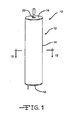
- FIGs. 1 and 13 show a capacitor 10 according to the present invention.
- Capacitor 10 has an elongated cylindrical shape with a casing 12 having a cylindrical casing sidewall or tube 14 extending to closed first and second end walls 16 and 18.
- the second end wall 18 may be formed separately as a cap that is fitted to the tubular sidewall 14 and sealed thereto to form a casing container.
- the first end wall 16 may also be formed as a cap that functions as a header for the casing container and for sealing an anode terminal pin or lead 20 therein. In later parts of this specification, the end wall 16 will be referred to as casing header 16.
- the capacitor 10 comprises an anode assembly 22 of two side-by-side anodes 24 and 26, which are each formed as pellets of an anode active material.
- a cathode 28 ( FIG. 13 ) is wrapped around the anode pellets 24, 26.
- the anode assembly 22 and cathode 28 are hermetically sealed inside the casing 12 and operatively associated with each other by a working electrolyte (not shown) contained therein.
- the capacitor 10 is of an electrolytic type with the cathode 28 comprising a conductive substrate supporting cathode active material having capacitive properties.
- the cathode 28 will be described in detail hereinafter.
- the anodes 24, 26 may be formed as pellets of a powdered metal selected from the group consisting of tantalum, aluminum, titanium, niobium, zirconium, hafnium, tungsten, molybdenum, vanadium, silicon, germanium, and mixtures thereof.
- the preferred metal is tantalum powder compressed into a semicylindrical shape as shown for anodes 24 and 26.
- the anode assembly 22 has a cylindrical shape corresponding to the cylindrical shape of the casing 12 with a diameter slightly less than the casing diameter.
- the anode 24 is comprised of a radiused anode sidewall 30 meeting a planar sidewall 32 extending to first and second anode end walls 34 and 36.
- the anode 26 is comprised of a radiused anode sidewall 38 meeting a planar sidewall 40 extending to first and second anode end walls 42 and 44.
- the anodes 24 and 26 are in a side-by-side relationship having their respective planar sidewalls 32 and 40 facing each other.
- Embedded anode wires or leads 46 and 48 extend from the respective end walls 34 and 42 of the anodes 24 and 26.
- the anode leads 46, 48 are preferably made of the same material as the anode active material.
- the anode pellets 24 and 26 are sintered under a vacuum at high temperatures and then anodized in a suitable electrolyte.
- the anodizing electrolyte fills the pores of the pressed powder bodies and a continuous dielectric oxide is formed thereon. In that manner, the anode pellets 24 and 26 and their extending leads 46 and 48 are provided with a dielectric oxide layer formed to a desired working voltage.
- the anodes 24 and 26 can also be of an etched aluminum, niobium, or titanium foil.
- the anodes 24 and 26 are brought into proximity with each other in the side-by-side relationship shown in FIGs. 4 and 5 .
- the dielectric oxide is removed from the distal ends of the anode leads 46 and 48 and they are electrically connected to the anode terminal lead 20.
- the electrical connection of the anode leads 46 and 48 to the terminal lead 20 is made by joining each of them to a conductive junction bar 50.
- the bar 50 is formed as a substantially rectangular slab of conductive material, although shapes other than rectangular may be suitable.
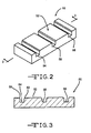
- the junction bar 50 is comprised of a surface 52 having a plurality of notches or grooves 54, 56, and 58 formed therein. Each of the grooves 54, 56, 58 is dimensioned to receive one of the anode leads 46 or 48, or the terminal lead 20.
- the grooves provided in the bar 50 of FIGs. 2 and 3 are substantially rectangular in cross-section. Groove shapes other than rectangular or square may also be suitable.
- the anode lead 46 of the first anode 24 is disposed in groove 54
- the anode lead 48 of the second anode 26 is disposed in groove 56
- the terminal lead 20 is disposed in groove 58 intermediate grooves 54 and 56.
- Each of the grooves 54, 56 and 58 may be provided with chamfers, such as chamfers 60 and 62 of groove 54, to guide placement of the leads into their respective grooves during the anode assembly fabrication process.
- the junction bar 50 may be manufactured by various processes including but not limited to micro-machining, water jet cutting, chemical etching, punching, and fine blanking.
- each of the leads 46, 48 and 20 may be joined to the bar 50 within their respective grooves 54, 56, 58 by dimensioning the grooves so that the leads are nested therein.
- the leads 46, 48 and 20 are joined to the junction bar 50 by welding.
- the bar 50 is made of a metal that is weldable to the leads. Suitable materials include tantalum, titanium, nickel, molybdenum, niobium, cobalt, stainless steel, tungsten, platinum, palladium, gold, silver, copper, chromium, vanadium, aluminum, zirconium, hafnium, zinc, iron, and mixtures and alloys thereof.
- the junction bar is of the same metal as the leads.
- the anodes 24 and 26, the leads 46, 48 and 20 and the junction bar 50 may all be made of tantalum.
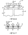
- FIG. 6 is a side elevation view of the anode assembly of FIG. 4 , showing the anode leads 46, 48 and terminal lead 20 disposed in the respective grooves 54, 56 and 58 provided in the junction bar 50.
- One sequential path for the operation of a welder is indicated by arrows 64, 66, 68 and 70, wherein lead 48 is welded to groove 56, lead 20 is welded to groove 58, and lead 46 is welded to groove 54.
- the leads 46, 48 and 20 are preferably "double welded" along both contact lines formed with the respective grooves 54, 56 and 58.
- Lead 48 is joined to groove 56 by welds 72 and 74.
- Lead 20 is joined to groove 58 by welds 76 and 78.
- lead 46 is joined to groove 54 by weld 80 and 82, the latter being shown in the process of being welded by laser 84.
- the leads 46, 48 and 20 are preferably dimensioned so as to be press-fitted into their respective grooves 54, 56, and 58. In that manner, no additional tooling is required to hold them in place until they are fully secured by welding.
- the welding process is preferably carried out under vacuum.
- the welding process may be performed in an inert atmosphere, such as nitrogen (N 2 ) or argon.
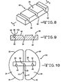
- FIGs. 8 to 10 illustrate yet another embodiment of a junction bar 86 for electrically connecting two anode leads to the terminal lead of a capacitor.
- the bar 86 is formed as a substantially rectangular slab of conductive material and is comprised of a surface 88 having a plurality of grooves 90, 92 and 94 formed therein.
- Each of the grooves 90, 92 and 94 is dimensioned to receive one of the anode leads 46 or 48, or the terminal lead 20.
- the grooves 90, 92 and 94 are substantially semi-circular in cross-section.
- a tool may be provided for holding the leads in place until connection to the junction bar 86 is complete.
- the grooves 90, 92 and 94 may include additional opposed planar portions.
- groove 90 is comprised of a semi-circular portion 96 and opposed planar portions 98 and 100. In that manner, the depth of the grooves 90, 92 and 94 is increased.
- the leads can be recessed deeper into their respective grooves, and stronger welds between the leads 46, 48 and 20 and the junction bar 86 can be attained.
- FIG. 10 it is shown that the anode lead 46 of the first anode 24 is disposed in groove 90, the anode lead 48 of the second anode 26 is disposed in groove 92, and the terminal lead 20 is disposed in groove 94.
- welds are provided to join the leads 46, 48 and 20 to the junction bar 86.
- the arc portion of the grooves 46, 48 and 20 is slightly greater than 180 degrees, such that the leads snap-fit into their respective grooves.
- junction bar 200 does not necessarily need to be a solid conductive object such as a metal bar.
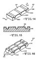
- FIGs. 14 and 15 illustrate an alternate embodiment of a junction bar 200 having a shape similar to that of junction bar 50.
- Junction bar 200 comprises a body 202 of a polymeric or some other non-conductive material.
- the body includes grooves 202A, 202B and 202C for receiving the leads 46, 48 and 20 therein.
- An upper plate 204 is supported thereon and has a shape conforming to that of the body 202 including its grooves.
- Plate 204 is of an electrically conductive material such as of those previously described as useful for junction bar 50, but preferably of tantalum. Electrical conductivity is then provided from the anode leads 46 and 48 through the conductive plate 204 and to the terminal lead 20.
- FIG. 16 shows another embodiment of a junction bar 210 having a shape similar to that of junction bar 50.
- Junction bar 210 comprises a body 212 of a polymeric or some other non-conductive material.
- the body includes grooves 212A, 212B and 212C for receiving the leads 46, 48 and 20 therein.
- At least one conductive strip 214 having a generally rectangular cross-section and a width that is significantly less than that of the body 212 is supported thereon.
- the conductive strips are of an electrically conductive material such as of any of those previously described as useful for junction bar 50, but preferably of tantalum. Electrical conductivity is then provided from the anode leads 46 and 48 through the conductive strips 214 and to the terminal lead 20.
- FIGs. 17 and 18 illustrate an alternate embodiment of a junction bar 220 having a shape similar to that of junction bar 50.
- Junction bar 220 comprises a body 222 of a polymeric or some other non-conductive material.
- the body 222 includes grooves 222A, 222B and 222C for receiving the leads 46, 48 and 20 therein.
- the body includes conductive fibers or wires 224 embedded therein.
- the fibers or wires 224 are of an electrically conductive material such as of those previously described as useful for junction bar 50, but preferably of tantalum. Electrical conductivity is then provided from the anode leads 46 and 48 through the conductive fibers or wires 224 and to the terminal lead 20.
- FIGs. 19 and 20 illustrate a further embodiment of a junction bar 230 having a shape similar to that of junction bar 50.
- Junction bar 230 comprises a body 232 of a polymeric or some other non-conductive material.
- the body includes grooves 232A, 232B and 232C for receiving the leads 46, 48 and 20 therein.
- At least one conductive rod 234 having a generally circular cross-section of a diameter that is significantly less than the width of the body 212 is supported thereon.
- the conductive rods are of an electrically conductive material such as of any of those previously described as useful for junction bar 50, but preferably of tantalum. Electrical conductivity is then provided from the anode leads 46 and 48 through the conductive rods 234 and to the terminal lead 20.
- the anode terminal lead 20 is sealed and electrically insulated from a casing lid or header.
- terminal lead 20 is sealed within a glass-to-metal seal formed within a through hole in the casing header 16.
- the header 16 comprises the first end wall previously described with respect to FIG. 1 and is a unitary metal member such as of titanium having a cylindrical shape in cross-section and comprising an upper planar surface 104 spaced from a lower planar surface 106.
- the header 16 includes a perimeter region 108 comprised of an outer diameter leading to a step that joins to a frusto-conical portion that steps down to an inner diameter portion.
- This perimeter configuration is provided for engagement with the sidewall 14 of the casing 12, and for optimal support and electrical connection with the cathode 28 ( FIG. 13 ) of capacitor 10. Additional details of one suitable configuration of the perimeter region 108 are provided in the aforementioned commonly owned U.S. Pat. No. 7,072,171 .
- a ferrule 110 for the glass-to-metal-seal (GTMS), which seals and electrically insulates the terminal pin 20 within the header 16 may be formed integrally with the header.
- the ferrule 110 has a cylindrical sidewall spaced inwardly from the inner diameter portion and comprises a lower side 112 spaced below the lower header surface 106.
- the GTMS comprises the ferrule 110 defining an internal cylindrical through bore or passage of constant inside diameter.
- An insulative glass 111 within the through bore provides a hermetic seal between the ferrule 110 and the anode terminal pin 20 passing there through.
- the insulative glass may be ELAN ® type 88 or MANSOLTM type 88.
- a relatively fast curing polymeric material such as a polyolefin, a fluoropolymer, a hot melt adhesive, or a UV curable adhesive may be filled into the space between the opposed planar end walls of the anode pellets 24 and 26 and the lower header surface 106 to the edge forming the inner diameter portion of the header.
- a relatively slow curing silastic material may also be useful.
- FIG. 12 is a side elevation view of a prior art capacitor including an anode assembly 114 having the terminal lead 116 thereof sealed within a glass-to-metal seal 118 of a capacitor casing header 120.
- the anode assembly 22 of FIG. 11 is advantageous over the prior art anode assembly 114 of FIG. 12 .
- more internal volume of the capacitor 10 ( FIG. 1 ) can be filled with electrode active materials, thereby increasing the overall energy density of the capacitor.
- no precision bends are required in the anode leads 46 and 48 to align them with their respective grooves in the junction bar 50.
- anode leads 122 and 124 of the prior art anode assembly 114 must be precisely bent to align them with the terminal pin 116 before they are joined together.
- the use of the junction bar 50 enables connection of the anode leads 46 and 48 to the terminal lead 20 to be made reliably and without the need for costly tooling to bend the leads and hold them in position against the terminal pin during welding.
- a capacitor that includes the anode assembly 22 of FIG. 4 or the anode assembly 102 of FIG. 8 is further comprised of a cathode comprising a conductive substrate supporting a cathode active material facing the first and second anodes, and a separator positioned between the first and second anodes and the cathode to prevent them from contacting each other.
- FIG. 13 is a cross-sectional view of one exemplary embodiment of such a capacitor 10, which includes the anode assembly 22 with anodes 24 and 26, and a cathode 28.
- the cathode 28 includes a conductive substrate 126 supporting a cathode active material 128 facing the sidewalls of the anodes 24 and 26.
- the cathode active material 128 is disposed on both sides of the conductive substrate 126 in the cathode portion that is located between the opposed planar side walls 32 and 40.
- the conductive substrate 126 is wrapped around the anodes 24 and 26 such that cathode active material 128 faces the radiused anode sidewalls 30 and 38 of the respective anodes 24 and 26. Further details of a cathode suitably configured according to the illustrated embodiment for use in the capacitor 10 may be found in the aforementioned U.S. Patent No. 7,072,171 .
- the substrate 126 is of a material selected from titanium, tantalum, nickel, molybdenum, niobium, cobalt, stainless steel, tungsten, platinum, palladium, gold, silver, copper, chromium, vanadium, aluminum, zirconium, hafnium, zinc, iron, and mixtures and alloys thereof.
- the substrates are of titanium and are from about 0.0005 inches to about 0.02 inches thick, preferably about 0.001 inches thick.
- the cathode active material 128 has a thickness of about a few hundred Angstroms to about 0.1 millimeters coated directly on the conductive substrate 126.
- the conductive substrate 126 may be of an anodized-etched conductive material, have a sintered active material with or without oxide contacted thereto, be contacted with a double layer capacitive material, for example a finely divided carbonaceous material such as activated graphite or activated carbon black, a redox, pseudocapacitive or an under potential material, or be an electroactive conducting polymer such as polyaniline, polypyrole, polythiophene, polyacetylene, and mixtures thereof.
- the redox or cathode active material 128 includes an oxide of a metal, the nitride of the metal, the carbon nitride of the metal, and/or the carbide of the metal, the oxide, nitride, carbon nitride and carbide having pseudocapacitive properties.
- the metal is preferably selected from the group consisting of ruthenium, cobalt, manganese, molybdenum, tungsten, tantalum, iron, niobium, iridium, titanium, zirconium, hafnium, rhodium, vanadium, osmium, palladium, platinum, nickel, lead gold, silver, cobalt, and mixtures thereof.
- the cathode active material 128 can also be an activated carbonaceous material such as carbon nanotubes or amorphous carbon.
- a separator of electrically insulative material in the shape of a bag completely surrounds and envelops each anode 24, 26 except their respective leads 46 and 48.
- Separator bags 130 and 132 may include seamed overlaps 134 and 136 extending longitudinally along the respective anodes 24, 26.
- the separator prevents an internal electrical short circuit between the anode pellets 24, 26 of the anode assembly 22 and the cathode active material 128 in the assembled capacitor and has a degree of porosity sufficient to allow flow there through of the working electrolyte during the electrochemical reaction of the capacitor 10.
- Illustrative separator materials include woven and non-woven fabrics of polyolefinic fibers including polypropylene and polyethylene or fluoropolymeric fibers including polyvinylidene fluoride, polyethylenetetrafluoroethylene, and polyethylenechlorotrifluoroethylene laminated or superposed with a polyolefinic or fluoropolymeric microporous film, non-woven glass, glass fiber materials and ceramic materials.
- Suitable microporous films include a polyethylene membrane commercially available under the designation SOLUPOR ® (DMS Solutech), a polytetrafluoroethylene membrane commercially available under the designations EXCELLERATORTM (W.R.
- Cellulose based separators also typically used in capacitors are contemplated by the scope of the present invention. Depending on the electrolyte used, the separator can be treated to improve its wettability, as is well known by those skilled in the art.
- the thusly-constructed electrode assembly including the anodes 24 and 26, the cathode 28, the separator bags 130 and 132, and the header 16 is next fitted to a casing tube 14.
- the tube 14 is a cylindrically shaped member that is open at both of its ends and made of the same metal as the header 16, for example, titanium. With the electrode assembly housed therein, the upper open-end of the tube 14 fits into a corresponding outer step of the header 16. Laser welding then hermetically seals the tube 14 to the header 16 at this junction.
- the lower ends of the anode pellets 24, 26 and the lower edge of the conductive substrate 126 of the associated cathode 24 are spaced from the lower open end of the tube 14.
- a lower lid 18 ( FIG. 1 ) is fitted in the lower open end of the tube 14 to close the capacitor 10.
- the lower lid 18 is a unitary metal member of the same material as the header 16 and casing tube 14.
- the lower lid 18 has a cylindrical shape in cross-section and comprises an upper planar surface spaced from a lower planar surface, and an outer diameter leading to a step that joins to a frusto-conical portion tapering downwardly and inwardly to the lower surface.
- the step is sized to fit into the lower open-end of the tube 14 in a snug-fitting relationship and is hermetically sealed therein, preferably by laser welding. In that manner, the header 16 closing the upper open end of the tube 14 and the lower lid 18 closing the lower open end form the casing 12 for the capacitor 10.
- the lower lid 18 may be further provided with an opening (not shown) for filling a working electrolyte (not shown) into the casing. After the electrolyte is filled into the capacitor 10, a plug (not shown) is sealed in the opening by laser welding to hermetically close the casing 12.
- junction bar 50, 86, 200, 210, 220 and 230 to connect capacitor anode leads to a terminal lead
- the capacitor may be comprised of three or more anodes as described in the aforementioned commonly owned U.S. Provisional Application Serial No. 61/050,716, filed May 6, 2008 .
- the leads of the three or more anodes may be connected to a terminal lead by joining them to a junction bar. Since the leads may not necessarily be oriented in a straight line as in the anode assembly 22 of FIG.
- the grooves provided in the junction bar for receiving the leads may be cut to different depths, or located on different surfaces.
- the junction bar may have a shape differing from the simple rectangular shape of junction bars 50, 86 200, 210, 220 and 230 of respective FIGs. 2 , 7 , 14, 16 , 17 and 19 .
- the leads may be offset in their respective anode pellets such that in the overall anode assembly, they are disposed in a straight line to enable connection to a common surface of the junction bar.
Landscapes
- Engineering & Computer Science (AREA)
- Power Engineering (AREA)
- Manufacturing & Machinery (AREA)
- Microelectronics & Electronic Packaging (AREA)
- Fixed Capacitors And Capacitor Manufacturing Machines (AREA)
Claims (15)
- Anodenbaugruppe für einen Kondensator, wobei die Anodenbaugruppe dadurch gekennzeichnet ist, dass sie Folgendes umfasst:a) einen Verbindungssteg, die ein leitfähiges Material und mindestens eine erste Nut, eine zweite Nut und eine dritte Nut umfasst;b) eine erste Anode, die eine erste leitfähige Leitung umfasst, die in der ersten Verbindungsstegnut angeordnet ist;c) eine zweite Anode, die eine zweite leitfähige Leitung umfasst, die in der zweiten Verbindungsstegnut angeordnet ist; undd) eine Anodenanschlussleitung, die in der dritten Verbindungsstegnut angeordnet ist.
- Anodenbaugruppe nach Anspruch 1, dadurch gekennzeichnet, dass das leitfähige Material für den Verbindungssteg aus der Gruppe ausgewählt ist, die aus Folgendem besteht: Tantal, Titan, Nickel, Molybdän, Niob, Kobalt, Edelstahl, Wolfram, Platin, Palladium, Gold, Silber, Kupfer, Chrom, Vanadium, Aluminium, Zirkonium, Hafnium, Zink, Eisen und Mischungen und Legierungen davon.
- Anodenbaugruppe nach Anspruch 1 oder Anspruch 2, dadurch gekennzeichnet, dass der Verbindungssteg aus einem elektrisch nicht leitfähigen Material besteht, das mit einem elektrisch leitfähigen Material versehen ist, das aus der Gruppe ausgewählt ist, die aus Folgendem besteht: einer Platte, die darauf gestützt wird, mindestens einem Streifen, der darauf gestützt wird, mindestens einer Stange, die darauf gestützt wird, eingebetteten Fasern und eingebetteten Drähten.
- Anodenbaugruppe nach einem der Ansprüche 1 bis 3, dadurch gekennzeichnet, dass die erste, zweite und dritte Nut im Querschnitt rechteckig oder halbkreisförmig ist.
- Anodenbaugruppe nach einem der Ansprüche 1 bis 4, dadurch gekennzeichnet, dass die erste Anodenleitung, die zweite Anodenleitung und die Anschlussleitung im Presssitz in der jeweiligen ersten, zweiten und dritten Nut des Verbindungsstegs angeordnet sind.
- Anodenbaugruppe nach einem der Ansprüche 1 bis 4, dadurch gekennzeichnet, dass die erste Anodenleitung, die zweite Anodenleitung und die Anschlussleitung durch Schweißen mit dem Verbindungssteg verbunden ist.
- Anodenbaugruppe nach einem der Ansprüche 1 bis 6, dadurch gekennzeichnet, dass jede Anode einen abgerundeten Anodenseitenwandabschnitt umfasst, der auf einen ebenen Seitenwandabschnitt trifft, der sich zu einer ersten und zweiten Anodenendwand erstreckt, und wobei die Anoden in einer Seite-an-Seite-Beziehung angeordnet sind und ihre jeweiligen ebenen Seitenwandabschnitte einander zugewandt sind.
- Kondensator, der dadurch gekennzeichnet ist, dass er Folgendes umfasst:a) ein Gehäuse;b) einen Verbindungssteg der Anodenbaugruppe nach Anspruch 1, der auf einem leitfähigen Material und mindestens einer ersten Nut, einer zweiten Nut und einer dritten Nut basiert;c) eine Anodenbaugruppe, die Folgendes umfasst: mindestens eine erste Anode, die eine erste leitfähige Leitung umfasst, die in der ersten Verbindungsstegnut angeordnet ist, und eine zweite Anode, die eine zweite leitfähige Leitung umfasst, die in der zweiten Verbindungsstegnut angeordnet ist;d) eine Anodenanschlussleitung, die in der dritten Verbindungsstegnut angeordnet ist;e) eine Kathode, die ein leitfähiges Substrat umfasst, das ein aktives Kathodenmaterial umfasst, das der ersten und zweiten Anode zugewandt ist;f) ein Trennelement, das zwischen der ersten und zweiten Anode und der Kathode angeordnet ist, um zu verhindern, dass diese miteinander in Kontakt kommen; undg) einen Arbeitselektrolyten, der innerhalb des Gehäuses enthalten ist.
- Kondensator nach Anspruch 8, der das Merkmal oder die Merkmale aufweist, die in einem der Ansprüche 2 bis 7 aufgeführt sind.
- Verfahren zur Herstellung eines Kondensators, das folgende Schritte umfasst:a) Bereitstellen eines Verbindungsstegs der Anodenbaugruppe nach Anspruch 1, der auf einem leitfähigen Material und mindestens einer ersten Nut, einer zweiten Nut und einer dritten Nut basiert; und mindestens eine erste Anode, die eine erste leitfähige Leitung, eine zweite Anode, die eine zweite leitfähige Leitung, und eine Anodenanschlussleitung umfasst;b) Versiegeln der Anodenanschlussleitung an einem Gehäusedeckel und elektrisches Isolieren der Anodenanschlussleitung gegen einen Gehäusedeckel;c) Verbinden der ersten leitfähigen Leitung mit der ersten Verbindungsstegnut, Verbinden der zweiten leitfähigen Leitung mit der zweiten Verbindungsstegnut, und Verbinden der Anschlussleitung mit der dritten Verbindungsstegnut;d) Bereitstellen einer Kathode, die ein erstes leitfähiges Substrat umfasst, das ein aktives Kathodenmaterial umfasst, das den Anoden zugewandt ist, jedoch durch ein Zwischentrennelement an einem Kontakt damit gehindert wird, um dadurch eine Elektrodenbaugruppe zu bilden;e) Versiegeln des Gehäusedeckels an einem Gehäuse, um die Elektrodenbaugruppe zu umschließen; undf) Einfüllen eines Arbeitselektrolyten in das Gehäuse über eine Füllöffnung und Abdichten der Füllöffnung.
- Verfahren nach Anspruch 10, das das Auswählen des leitfähigen Materials für den Verbindungssteg aus der Gruppe umfasst, die aus Folgendem besteht: Tantal, Titan, Nickel, Molybdän, Niob, Kobalt, Edelstahl, Wolfram, Platin, Palladium, Gold, Silber, Kupfer, Chrom, Vanadium, Aluminium, Zirkonium, Hafnium, Zink, Eisen und Mischungen und Legierungen davon.
- Verfahren nach Anspruch 10 oder Anspruch 11, das das Bereitstellen des Verbindungsstegs aus einem elektrisch nicht leitfähigen Material umfasst, das mit einem elektrisch leitfähigen Material versehen ist, das aus der Gruppe ausgewählt ist, die aus Folgendem besteht: einer Platte, die darauf gestützt wird, mindestens einem Streifen, der darauf gestützt wird, mindestens einer Stange, die darauf gestützt wird, eingebetteten Fasern und eingebetteten Drähten.
- Verfahren nach einem der Ansprüche 10 bis 12, das umfasst, dass die erste, zweite und dritte Nut im Querschnitt rechteckig oder halbkreisförmig bereitgestellt wird.
- Verfahren nach einem der Ansprüche 10 bis 13, das den Presssitz der ersten Anodenleitung, der zweiten Anodenleitung und der Anschlussleitung in die jeweilige erste, zweite und dritte Nut des Verbindungsstegs umfasst.
- Verfahren nach einem der Ansprüche 10 bis 13, das das Verschweißen der ersten Anodenleitung, der zweiten Anodenleitung und der Anschlussleitung mit dem Verbindungssteg umfasst.
Applications Claiming Priority (1)
| Application Number | Priority Date | Filing Date | Title |
|---|---|---|---|
| US98046907P | 2007-10-17 | 2007-10-17 |
Publications (2)
| Publication Number | Publication Date |
|---|---|
| EP2051265A1 EP2051265A1 (de) | 2009-04-22 |
| EP2051265B1 true EP2051265B1 (de) | 2015-12-02 |
Family
ID=40263240
Family Applications (1)
| Application Number | Title | Priority Date | Filing Date |
|---|---|---|---|
| EP08166842.8A Ceased EP2051265B1 (de) | 2007-10-17 | 2008-10-16 | Verbindungen für multiple Kondensatoren Anoden |
Country Status (2)
| Country | Link |
|---|---|
| US (1) | US8081419B2 (de) |
| EP (1) | EP2051265B1 (de) |
Families Citing this family (10)
| Publication number | Priority date | Publication date | Assignee | Title |
|---|---|---|---|---|
| GB2512486B (en) * | 2013-03-15 | 2018-07-18 | Avx Corp | Wet electrolytic capacitor |
| USRE48439E1 (en) | 2013-09-06 | 2021-02-16 | Greatbatch Ltd. | High voltage tantalum anode and method of manufacture |
| US9633796B2 (en) | 2013-09-06 | 2017-04-25 | Greatbatch Ltd. | High voltage tantalum anode and method of manufacture |
| US9312075B1 (en) | 2013-09-06 | 2016-04-12 | Greatbatch Ltd. | High voltage tantalum anode and method of manufacture |
| KR102163038B1 (ko) * | 2015-01-27 | 2020-10-08 | 삼성전기주식회사 | 탄탈륨 커패시터 |
| US9870868B1 (en) | 2016-06-28 | 2018-01-16 | Avx Corporation | Wet electrolytic capacitor for use in a subcutaneous implantable cardioverter-defibrillator |
| US9870869B1 (en) | 2016-06-28 | 2018-01-16 | Avx Corporation | Wet electrolytic capacitor |
| CN109715320A (zh) | 2016-08-12 | 2019-05-03 | 复合材料技术公司 | 电解电容器和改进电解电容器阳极的方法 |
| KR20190077321A (ko) | 2016-09-01 | 2019-07-03 | 컴포짓 매터리얼스 테크놀로지, 아이엔씨. | LIB 애노드용 밸브 금속 기판상의 나노-스케일/나노 구조화된 Si 코팅 |
| US11831030B2 (en) | 2018-05-22 | 2023-11-28 | Pacesetter, Inc. | Method of forming a brazed joint having molybdenum material |
Family Cites Families (20)
| Publication number | Priority date | Publication date | Assignee | Title |
|---|---|---|---|---|
| US3456157A (en) * | 1967-06-12 | 1969-07-15 | Mallory & Co Inc P R | Electronic assembly |
| JPS5537852B2 (de) * | 1975-02-14 | 1980-09-30 | ||
| JPH0672204U (ja) * | 1993-03-17 | 1994-10-07 | 北陸電気工業株式会社 | 高圧用電子部品及び高圧用可変抵抗器 |
| US5538607A (en) * | 1995-04-12 | 1996-07-23 | Pate; Ray H. | Anode assembly comprising an anode bar for the production of molten metal by electrolysis |
| JP3755336B2 (ja) * | 1998-08-26 | 2006-03-15 | 松下電器産業株式会社 | 固体電解コンデンサおよびその製造方法 |
| US6200156B1 (en) * | 1998-11-27 | 2001-03-13 | Hokuriku Electric Industry Co., Ltd. | Terminal fitment for lead wire connection and high-voltage variable resistor unit with relay terminal fitment |
| TW516054B (en) * | 2000-05-26 | 2003-01-01 | Matsushita Electric Industrial Co Ltd | Solid electrolytic capacitor |
| JP2001345204A (ja) * | 2000-06-02 | 2001-12-14 | Murata Mfg Co Ltd | 高圧可変抵抗器 |
| JP2002075807A (ja) | 2000-08-31 | 2002-03-15 | Matsushita Electric Ind Co Ltd | 固体電解コンデンサおよびその製造方法 |
| JP3532519B2 (ja) * | 2000-11-22 | 2004-05-31 | Necトーキン株式会社 | チップ型コンデンサの製造方法およびその製造装置 |
| US6625009B2 (en) * | 2001-04-05 | 2003-09-23 | Rohm Co., Ltd. | Solid electrolytic capacitor and method of making the same |
| JP2003068576A (ja) * | 2001-08-30 | 2003-03-07 | Rohm Co Ltd | 面実装型固体電解コンデンサの構造及びその製造方法 |
| JP2003133183A (ja) * | 2001-10-26 | 2003-05-09 | Matsushita Electric Ind Co Ltd | 固体電解コンデンサおよびその製造方法 |
| JP2004103981A (ja) * | 2002-09-12 | 2004-04-02 | Sanyo Electric Co Ltd | 固体電解コンデンサの製造方法及びこの方法によって製造される固体電解コンデンサ |
| JP2005166832A (ja) * | 2003-12-01 | 2005-06-23 | Rohm Co Ltd | 固体電解コンデンサ |
| JP2005166833A (ja) * | 2003-12-01 | 2005-06-23 | Rohm Co Ltd | 面実装型固体電解コンデンサ及びその製造方法 |
| JP2005166975A (ja) * | 2003-12-03 | 2005-06-23 | Sanyo Electric Co Ltd | 電気二重層コンデンサ、電解質電池及びこれらの製造方法 |
| JP4657204B2 (ja) * | 2004-03-30 | 2011-03-23 | ローム株式会社 | 固体電解コンデンサ |
| US7342775B2 (en) * | 2004-04-23 | 2008-03-11 | Kemet Electronics Corporation | Fluted anode with minimal density gradients and capacitor comprising same |
| KR101023277B1 (ko) * | 2004-05-28 | 2011-03-18 | 파나소닉 주식회사 | 콘덴서 및 그 제조방법 |
-
2008
- 2008-10-14 US US12/250,598 patent/US8081419B2/en not_active Expired - Fee Related
- 2008-10-16 EP EP08166842.8A patent/EP2051265B1/de not_active Ceased
Also Published As
| Publication number | Publication date |
|---|---|
| US8081419B2 (en) | 2011-12-20 |
| EP2051265A1 (de) | 2009-04-22 |
| US20090103246A1 (en) | 2009-04-23 |
Similar Documents
| Publication | Publication Date | Title |
|---|---|---|
| EP2051265B1 (de) | Verbindungen für multiple Kondensatoren Anoden | |
| EP2117021B1 (de) | Elektrolytkondensatoren mit mehreren Anoden und Anodenanschlusskonfiguration dafür | |
| US7072171B1 (en) | Electrolytic capacitor capable of insertion into the vasculature of a patient | |
| US7092242B1 (en) | Polymeric restraints for containing an anode in an electrolytic capacitor from high shock and vibration conditions | |
| JP4726784B2 (ja) | 電気化学的装置用の絶縁性フィードスルー組立体 | |
| US7085126B2 (en) | Molded polymeric cradle for containing an anode in an electrolytic capacitor from high shock and vibration conditions | |
| EP0877400B1 (de) | Hermetisch geschlossener Kondensator | |
| EP1936643B1 (de) | Kondensator mit mehreren intern verbundenen Anoden | |
| US20080068779A1 (en) | Flat Sealing Of Anode/Separator Assembly For Use In Capacitors | |
| EP3171378B1 (de) | Hochspannungskondensator mit dualer tantalanoden/kathoden-stromabnehmerelektrodenanordnung, die in einer konstruktion mit zwei separatorhüllen untergebracht ist | |
| EP3163593B1 (de) | Hochspannungstantalkondensator mit verbessertem kathoden-/separatorentwurf | |
| US6967829B2 (en) | Capacitor interconnect design | |
| US20040260354A1 (en) | Miniature compression feedthrough assembly for electrochemical devices | |
| EP3166117A1 (de) | Hochspannungsdoppelanodentantalkondensator mit zugewandten gehäuseschalen mit kontaktierung einer zwischentrennwand | |
| US11195665B2 (en) | Titanium clad nickel termination-pad welded to a titanium tab for a capacitor | |
| EP1571681B1 (de) | Gegossene polymere Aufnahmevorrichtung zur Aufnahme einer Anode in einem Elektrolytkondensator zur Verwendung unter Bedingungen mit hoher Stoss- und Schwingungsbelastung | |
| US12368006B2 (en) | Capacitor with stepped cathode | |
| US20040219425A1 (en) | Electric coupling of a connection to a terminal |
Legal Events
| Date | Code | Title | Description |
|---|---|---|---|
| PUAI | Public reference made under article 153(3) epc to a published international application that has entered the european phase |
Free format text: ORIGINAL CODE: 0009012 |
|
| AK | Designated contracting states |
Kind code of ref document: A1 Designated state(s): AT BE BG CH CY CZ DE DK EE ES FI FR GB GR HR HU IE IS IT LI LT LU LV MC MT NL NO PL PT RO SE SI SK TR |
|
| AX | Request for extension of the european patent |
Extension state: AL BA MK RS |
|
| 17P | Request for examination filed |
Effective date: 20091012 |
|
| 17Q | First examination report despatched |
Effective date: 20091102 |
|
| AKX | Designation fees paid |
Designated state(s): DE FR IT SE |
|
| GRAP | Despatch of communication of intention to grant a patent |
Free format text: ORIGINAL CODE: EPIDOSNIGR1 |
|
| INTG | Intention to grant announced |
Effective date: 20150617 |
|
| GRAS | Grant fee paid |
Free format text: ORIGINAL CODE: EPIDOSNIGR3 |
|
| GRAA | (expected) grant |
Free format text: ORIGINAL CODE: 0009210 |
|
| AK | Designated contracting states |
Kind code of ref document: B1 Designated state(s): DE FR IT SE |
|
| REG | Reference to a national code |
Ref country code: DE Ref legal event code: R096 Ref document number: 602008041368 Country of ref document: DE |
|
| PG25 | Lapsed in a contracting state [announced via postgrant information from national office to epo] |
Ref country code: SE Free format text: LAPSE BECAUSE OF FAILURE TO SUBMIT A TRANSLATION OF THE DESCRIPTION OR TO PAY THE FEE WITHIN THE PRESCRIBED TIME-LIMIT Effective date: 20151202 |
|
| PG25 | Lapsed in a contracting state [announced via postgrant information from national office to epo] |
Ref country code: IT Free format text: LAPSE BECAUSE OF FAILURE TO SUBMIT A TRANSLATION OF THE DESCRIPTION OR TO PAY THE FEE WITHIN THE PRESCRIBED TIME-LIMIT Effective date: 20151202 |
|
| REG | Reference to a national code |
Ref country code: DE Ref legal event code: R097 Ref document number: 602008041368 Country of ref document: DE |
|
| REG | Reference to a national code |
Ref country code: FR Ref legal event code: PLFP Year of fee payment: 9 |
|
| PLBE | No opposition filed within time limit |
Free format text: ORIGINAL CODE: 0009261 |
|
| STAA | Information on the status of an ep patent application or granted ep patent |
Free format text: STATUS: NO OPPOSITION FILED WITHIN TIME LIMIT |
|
| 26N | No opposition filed |
Effective date: 20160905 |
|
| REG | Reference to a national code |
Ref country code: FR Ref legal event code: PLFP Year of fee payment: 10 |
|
| REG | Reference to a national code |
Ref country code: FR Ref legal event code: PLFP Year of fee payment: 11 |
|
| PGFP | Annual fee paid to national office [announced via postgrant information from national office to epo] |
Ref country code: FR Payment date: 20180913 Year of fee payment: 11 |
|
| PGFP | Annual fee paid to national office [announced via postgrant information from national office to epo] |
Ref country code: DE Payment date: 20181002 Year of fee payment: 11 |
|
| REG | Reference to a national code |
Ref country code: DE Ref legal event code: R119 Ref document number: 602008041368 Country of ref document: DE |
|
| PG25 | Lapsed in a contracting state [announced via postgrant information from national office to epo] |
Ref country code: DE Free format text: LAPSE BECAUSE OF NON-PAYMENT OF DUE FEES Effective date: 20200501 |
|
| PG25 | Lapsed in a contracting state [announced via postgrant information from national office to epo] |
Ref country code: FR Free format text: LAPSE BECAUSE OF NON-PAYMENT OF DUE FEES Effective date: 20191031 |