EP2040317A2 - Lösungsprozessiertes organisches elektronisches Bauelement mit verbesserter Elektrodenschicht - Google Patents
Lösungsprozessiertes organisches elektronisches Bauelement mit verbesserter Elektrodenschicht Download PDFInfo
- Publication number
- EP2040317A2 EP2040317A2 EP08164755A EP08164755A EP2040317A2 EP 2040317 A2 EP2040317 A2 EP 2040317A2 EP 08164755 A EP08164755 A EP 08164755A EP 08164755 A EP08164755 A EP 08164755A EP 2040317 A2 EP2040317 A2 EP 2040317A2
- Authority
- EP
- European Patent Office
- Prior art keywords
- layer
- interface
- cesium salt
- intermediate layer
- contained
- Prior art date
- Legal status (The legal status is an assumption and is not a legal conclusion. Google has not performed a legal analysis and makes no representation as to the accuracy of the status listed.)
- Granted
Links
Images


Classifications
-
- H—ELECTRICITY
- H10—SEMICONDUCTOR DEVICES; ELECTRIC SOLID-STATE DEVICES NOT OTHERWISE PROVIDED FOR
- H10K—ORGANIC ELECTRIC SOLID-STATE DEVICES
- H10K50/00—Organic light-emitting devices
- H10K50/80—Constructional details
- H10K50/805—Electrodes
- H10K50/82—Cathodes
-
- H—ELECTRICITY
- H10—SEMICONDUCTOR DEVICES; ELECTRIC SOLID-STATE DEVICES NOT OTHERWISE PROVIDED FOR
- H10K—ORGANIC ELECTRIC SOLID-STATE DEVICES
- H10K50/00—Organic light-emitting devices
- H10K50/10—OLEDs or polymer light-emitting diodes [PLED]
- H10K50/17—Carrier injection layers
-
- H—ELECTRICITY
- H10—SEMICONDUCTOR DEVICES; ELECTRIC SOLID-STATE DEVICES NOT OTHERWISE PROVIDED FOR
- H10K—ORGANIC ELECTRIC SOLID-STATE DEVICES
- H10K50/00—Organic light-emitting devices
- H10K50/10—OLEDs or polymer light-emitting diodes [PLED]
- H10K50/17—Carrier injection layers
- H10K50/171—Electron injection layers
-
- H—ELECTRICITY
- H10—SEMICONDUCTOR DEVICES; ELECTRIC SOLID-STATE DEVICES NOT OTHERWISE PROVIDED FOR
- H10K—ORGANIC ELECTRIC SOLID-STATE DEVICES
- H10K30/00—Organic devices sensitive to infrared radiation, light, electromagnetic radiation of shorter wavelength or corpuscular radiation
- H10K30/80—Constructional details
- H10K30/81—Electrodes
-
- H—ELECTRICITY
- H10—SEMICONDUCTOR DEVICES; ELECTRIC SOLID-STATE DEVICES NOT OTHERWISE PROVIDED FOR
- H10K—ORGANIC ELECTRIC SOLID-STATE DEVICES
- H10K71/00—Manufacture or treatment specially adapted for the organic devices covered by this subclass
- H10K71/10—Deposition of organic active material
- H10K71/12—Deposition of organic active material using liquid deposition, e.g. spin coating
-
- H—ELECTRICITY
- H10—SEMICONDUCTOR DEVICES; ELECTRIC SOLID-STATE DEVICES NOT OTHERWISE PROVIDED FOR
- H10K—ORGANIC ELECTRIC SOLID-STATE DEVICES
- H10K85/00—Organic materials used in the body or electrodes of devices covered by this subclass
- H10K85/10—Organic polymers or oligomers
- H10K85/111—Organic polymers or oligomers comprising aromatic, heteroaromatic, or aryl chains, e.g. polyaniline, polyphenylene or polyphenylene vinylene
- H10K85/113—Heteroaromatic compounds comprising sulfur or selene, e.g. polythiophene
- H10K85/1135—Polyethylene dioxythiophene [PEDOT]; Derivatives thereof
-
- H—ELECTRICITY
- H10—SEMICONDUCTOR DEVICES; ELECTRIC SOLID-STATE DEVICES NOT OTHERWISE PROVIDED FOR
- H10K—ORGANIC ELECTRIC SOLID-STATE DEVICES
- H10K85/00—Organic materials used in the body or electrodes of devices covered by this subclass
- H10K85/40—Organosilicon compounds, e.g. TIPS pentacene
Definitions
- the invention relates to a solution-processed organic electronic component with an improved electrode layer.
- organic electronic components such as organic photodetectors, organic electrochromic devices and / or organic light-emitting diodes, which are based on so-called “small molecules”, particularly improved by the fact that they n- and / or p-doped organic semiconductor layers contained, which facilitated the injection of the respective charge carriers, ie, for example, that the OLEDs reach the same luminescence at lower operating voltage.
- This technique is for example from the WO 2005086251 A2 known.
- the cathode is made of a multi-layered, particularly advantageous from barium and aluminum.
- the barium is used because of its low work function as an electron source.
- the disadvantage of the technique is that barium is highly sensitive to oxidation, that is to say is unstable, and aluminum alone can not be used as the cathode material, since it has too high an injection barrier / work function.
- the object of the present invention is to provide an electrode for injecting electrons from a metal layer into the polymeric active organic semiconducting layer of the electronic component, which corresponds to n-doping.
- the invention relates to a solution-processed organic electronic component, a substrate, at least two single- or multi-layer electrodes, between at least one active organic semiconductive layer and between an electrode layer and an active organic semiconducting layer comprising an intermediate layer and / or an interface, characterized a cesium salt of an organic mono-, oligo- and polycarboxylic or sulphonic acid is contained as n-dopant in the intermediate layer / the interface.
- the interface is the layered region of two adjacent layers which are not necessarily sharply demarcated, in which, depending on the surface conditions of the respective layers or for other reasons, the exact material composition, for example compared to the layer center or the opposite layer surface, is changed. For example, by applying voltage on both sides of a charge carrier-added layer, the positive charge carriers migrate to the negative pole and the negative charge carriers move to the opposite side, whereas in the middle of the layer, an equal distribution of carriers will be observed. The interface is then the part of the layer in which an increase of one type of charge carrier is recorded.
- Polymeric organic electronic components are organic electronic components that comprise solution-processed long-chain organic layers.
- the properties of the materials suitable for liquid processes are achieved, for example, by the length of the alkyl groups. Likewise, various solvents can be used.
- the semiconducting organic material can be applied, for example, from solution, preferably from polar solvents, and can also be vapor-deposited, depending on the cesium salt used.
- the application preferably takes place via the known coating methods such as spin-coating, spraying, sputtering, etc.
- a lower, single-layer or multi-layer electrode is applied to a substrate, an organic semiconductive and active layer thereon, and finally a layer in which the use of the cesium salts according to the invention has been implemented.
- the electrode layer is applied to this intermediate layer for better electron injection from a metal electrode, such as an aluminum electrode.
- the materials are produced by reacting the free acids with heating with cesium carbonate in a polar solvent (butanol, ethanol or acetonitrile, etc.).
- the layer thickness of the emission layer is dependent on the emitter material and is typically less than 15 nm, that is to say in the range from 0.1 to 15 nm, in particular less than 10 nm and particularly preferably in the range from 3 to 5 nm.
- Metal electrode layers are preferably used as electrode layers, for example layers of aluminum, silver, gold, palladium, chromium, zinc, platinum, etc., as well as any alloys thereof.
- an alternative to the multilayer electrode using barium in organic electronic components is opened for the first time.
- an intermediate layer of at least one cesium salt is incorporated, by which it is possible that the operating voltage and luminescence of the organic component, so for example the OLED with respect to the OLED with barium as the electron injection layer at least of equal effectiveness (see figures of the characteristics).
- the invention describes the use of an alkali metal salt as an n-dopant for doping an organic semiconducting material to alter its electrical properties, wherein the alkali metal salt is an n-dopant with respect to the adjacent materials.
- the invention relates to a solution-processed organic electronic component with an improved electrode layer. Between the active organic layer and the electrode layer is either an interface or an interlayer, ie an intermediate layer in which a cesium salt is contained.
Landscapes
- Physics & Mathematics (AREA)
- Optics & Photonics (AREA)
- Electroluminescent Light Sources (AREA)
- Addition Polymer Or Copolymer, Post-Treatments, Or Chemical Modifications (AREA)
- Thin Film Transistor (AREA)
- Electrodes Of Semiconductors (AREA)
Abstract
Description
- Die Erfindung betrifft ein lösungsprozessiertes organisches elektronisches Bauelement mit einer verbesserten Elektrodenschicht.
- In den letzten Jahren wurden organische elektronische Bauelemente, wie beispielsweise organische Photodetektoren, organische elektrochrome Geräte und/oder organische Leuchtdioden, die basierend auf sogenannten "Small Molecules" aufgebaut sind, besonders dadurch verbessert, dass sie n- und/oder p-dotierte organische Halbleiterschichten enthielten, die die Injektion der jeweiligen Ladungsträger erleichterten, d.h. beispielsweise, dass die OLEDs bei geringerer Betriebsspannung die gleiche Lumineszenz erreichen. Diese Technik ist beispielsweise aus der
WO 2005086251 A2 bekannt. - Bei den aus Lösung prozessierten organischen elektronischen Bauelementen wie beispielsweise den polymeren OLEDs ist das Doping von Ladungsinjektionsschichten weitgehend unbekannt, da es schwierig ist, mehrere organische Materialien aus Lösung übereinander abzuscheiden ohne die darunterliegende Schicht/Schichten wieder ab- oder anzulösen.
- Um eine gute Elektroneninjektion in den polymeren Schichten organischer elektronischer Bauteile zu gewährleisten, wird beispielsweise die Kathode mehrschichtig ausgeführt, besonders vorteilhaft aus Barium und Aluminium. Dabei wird das Barium auf Grund seiner geringen Austrittsarbeit als Elektronenquelle benutzt.
- Der Nachteil der Technik ist, dass Barium stark oxidationsempfindlich, also instabil ist und Aluminium allein nicht als Kathodenmaterial eingesetzt werden kann, da es eine zu hohe Injektionsbarriere/Austrittsarbeit hat.
- Dabei dient die Anwendung des Aluminiums in der Mehrschichtelektrode mit Barium nur für einen primären Oxidationsschutz bei der Abdeckung der oxidationsempfindlichen Bariumschicht.
- Aufgabe der vorliegenden Erfindung ist es, eine Elektrode zur Injektion von Elektronen aus einer Metallschicht in die polymere aktive organische halbleitende Schicht des elektronischen Bauelements zur Verfügung zu stellen, was einem n-Doping entspricht.
- Gegenstand der Erfindung ist ein lösungsprozessiertes organisches elektronisches Bauelement, ein Substrat, zumindest zwei ein- oder mehrschichtige Elektroden, dazwischen mindestens eine aktive organische halbleitende Schicht und zwischen einer Elektrodenschicht und einer aktiven organischen halbleitenden Schicht eine Zwischenschicht und/oder ein Interface umfassend, dadurch gekennzeichnet, dass ein Cäsiumsalz einer organischen Mono-, Oligo- und Poly-Carbon- oder Sulfonsäure als n-Dopant in der Zwischenschicht/dem Interface enthalten ist.
- Als Interface wird der schichtförmige Bereich zweier benachbarter Schichten bezeichnet, die nicht notwendiger Weise scharf abgegrenzt vorliegen, in dem, den Oberflächenbedingungen der jeweiligen Schichten entsprechend oder aus sonstigen Gründen die genaue Materialzusammensetzung, beispielsweise im Vergleich zur Schichtmitte oder zur gegenüberliegenden Schichtoberfläche, verändert ist. Beispielsweise wandern durch Anlegen von Spannung auf beiden Seiten einer mit Ladungsträgern versetzten Schicht die Ladungsträger mit positiver Ladung zu dem negativen Pol und die Ladungsträger mit negativer Ladung auf die gegenüberliegende Seite, wohingegen in der Schichtmitte ein gleiche Verteilung der Ladungsträger zu beobachten sein wird. Als Interface wird dann der Teil der Schicht bezeichnet, in dem ein Anstieg einer Art von Ladungsträger zu verzeichnen ist.
- Allgemeine Formeln beispielhafter einfach und billig zugänglicher Cäsiumsalze, die gemäß der Erfindung eingesetzt werden können, sind im Folgenden dargestellt:
- 1) der Monocarbonsäuren:

- 2) der Alkansulfonsäuren:

- 3) der Dicarbonsäuren:

- 4) der Disulfonsäuren:

- 5) polymer gebundener Carbonsäuren:

- 6) polymer gebundener Sulfonsäuren

- Als polymere organische elektronische Bauteile werden organische elektronische Bauteile bezeichnet, die lösungsprozessierte langkettige organische Schichten umfassen.
- Die Eigenschaften der Materialien zur Eignung für Flüssigprozesse werden beispielsweise durch die Länge der Alkylgruppen erreicht. Ebenso können verschiedene Lösungsmittel eingesetzt werden.
- Das halbleitende organische Material ist beispielsweise aus Lösung, aus bevorzugt polaren Lösungsmitteln applizierbar, je nach eingesetztem Cäsiumsalz auch aufdampfbar. Die Aufbringung findet bevorzugt über die bekannten Beschichtungsverfahren wie spin-coating, Besprühen, Sputtern etc. statt.
- Zum Aufbau des elektronischen Bauteils wird auf einem Substrat eine untere, ein- oder mehrschichtige, Elektrode aufgebracht, darauf eine organische halbleitende und aktive Schicht und darauf schließlich eine Schicht, bei der die erfindungsgemäße Verwendung der Cäsiumsalze umgesetzt ist. Auf diese Zwischenschicht zur besseren Elektroneninjektion aus einer Metallelektrode wie beispielsweise einer Aluminium-elektrode wird die Elektrodenschicht aufgebracht.
- Die Herstellung der Materialien geschieht durch Umsetzung der freien Säuren unter Erwärmung mit Cäsiumcarbonat in einem polaren Lösungsmittel (Butanol, Ethanol oder Acetonitril etc.) Die Schichtdicke der Emissionsschicht ist abhängig vom Emittermaterial und typischerweise kleiner 15nm, also im Bereich von 0,1 bis 15 nm, insbesondere kleiner 10 nm und besonders bevorzugt im Bereich 3 bis 5 nm.
- Als Elektrodenschichten werden bevorzugt Metallelektrodenschichten eingesetzt wie beispielsweise Schichten aus Aluminium, Silber, Gold, Palladium, Chrom, Zink, Platin etc.. sowie beliebige Legierungen davon.
- Im Folgenden wird die Erfindung noch anhand von Ausführungsbeispielen näher erläutert:
- a) Darstellung von Cäsiumstearat:

- Eine Mischung von Cs2CO3 und Stearinsäure wird im Verhältnis 1:2 in Butanol vorgelegt und auf Rückfußtemperatur gehalten bis kein CO2 mehr gebildet wird. Danach wird Butanol am Rotationsverdampfer abgetrennt, der Rückstand mit Ether versetzt und abgesaugt, m.p.:263-269°C
- b) Darstellung von Dizäsiumsebazinat:
- Eine Mischung von Cs2CO3 und Sebazinsäure wird im Verhältnis 1:1 in Butanol vorgelegt und auf Rückfußtemperatur gehalten bis kein CO2 mehr gebildet wird. Danach wird Butanol am Rotationsverdampfer abgetrennt, der Rückstand mit Ether versetzt und abgesaugt.
- c) Darstellung des Zäsiumsalzes der Polystyrolsulfonsäure:
- Eine Mischung von Cs2CO3 und Polystyrolsulfonsäure 20%-wässrige Lösung wird im Verhältnis 1:2 vorgelegt und kurz erwärmt bis kein CO2 mehr gebildet wird. Danach wird Butanol zugesetzt und das Wasser sowie das Butanol am Rotationsverdampfer abgetrennt, der Rückstand wird mit Ether versetzt und abgesaugt.
- d) Darstellung des Zäsiumsalz eines carbonsäurefunktionalisierten Polyimids:
- d1) Synthese der Copolymeren
- d1a) Radikalische Polymerisation Unter absolut wasserfreien Bedingungen und unter einer sauerstofffreien Inertgasspülung werden 0,5 Mol Maleinsäureanhydrid und 0,5 Mol Trimethylallylsilan in 500 ml Dioxan gelöst und unter Zusatz von 2 Mol% AIBN (Azoisobuttersäurenitril) als Radikalstarter unter Rühren und Thermostatieren auf 50°C für 10h zur Reaktion gebracht. Im Anschluss daran wird das Lösungsmittel im Vakuum an einem Rotationsverdampfer vollständig entfernt. Tg : 200°C; Ausbeute quantitativ.

- D1b) imidisierende Kondensation 21,4g des nach Beispiel d1a erhaltenen Copolymer werden unter Rühren in 40ml Dimethylformamid gelöst und bei 50°C 2h erwärmt. Danach wird in Ethanol gefällt. Das gefällte Produkt wird bei 150°C in einem Trockenschrank getrocknet und dehydratisiert.

- d2) Synthese des Zäsiumsalzes: Eine Mischung von Cs2CO3 und Poly[trimethylsilylallyl-co-N-(4-carboxyphenyl)-maleinsäureimid wird im Verhältnis 1:2 in Acetonitril vorgelegt und bei Rückflusstemperatur erwärmt bis kein CO2 mehr gebildet wird. Danach wird das Acetonitril am Rotationsverdampfer abgetrennt, der Rückstand wird mit Ether versetzt und abgesaugt.
- e) Aufbau und Applikation der Schichten einer Polymer-OLED (Vergleich Stand der Technik, Zäsiumstearat durch Aufdampfen abgeschieden, Zäsiumstearat durch Spincoating abgeschieden):
- Beispielhafter Herstellungsprozess für das elektronische Bauteil:
- Spincoating PEDOT:PSS 60-80nm auf ITO-Substrat (Glas)
- Tempern der PEDOT-Schicht
- Spincoating eines LEP (Licht emittierenden Polymer) 70-100nm
- Spincoating der Organo-Zäsiumsalzschicht bzw. Aufdampfen der der Organo-Zäsiumsalzschicht bzw. Aufdampfen der Bariumschicht
- Aufdampfen der Aluminiumschicht
- Die Figuren zeigen Device-Kennlinien, wie sie mit dem vorgestellten Beispiel erreicht wurden:
- Die Struktur des Bauteils umfasste auf einem Substrat: I-TO/PEDOT:PSS (60nm)/White Polymer (70nm)/CsSt/Al
- Figur 1
- zeigt die Strom-Spannungs-Kennlinie
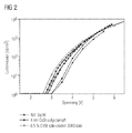
- Figur 2
- zeigt die Lumineszenz-Kennlinie
- Figur 3
- zeigt die Effizienz-Kennlinien:
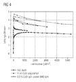
- Figur 4
- zeigt eine weitere Effizienz-Kennlinie.
- Wie in den
Figuren 1 und2 zu erkennen ist, fällt das Bauteil gegenüber der Referenz mit einer Barium-Aluminium-Elektrode in keiner Weise ab, sondern zeigt nahezu identische Strom-spannungs- und Lumineszenz-Werte.
- Die Struktur des Bauteils umfasste auf einem Substrat: I-TO/PEDOT:PSS (60nm)/White Polymer (70nm)/CsSt/Al
- Beispielhafter Herstellungsprozess für das elektronische Bauteil:
- In
Figuren 3 und4 ist zu erkennen, dass die Art und Weise der Aufbringung der Zäsiumschicht doch einen erheblichen Einfluss auf die Effizienz des Bauteils haben kann. - Mit der Erfindung wird erstmals eine Alternative zur mehrschichtigen Elektrode unter Verwendung von Barium in organischen elektronischen Bauteilen eröffnet. Dabei wird eine Zwischenschicht aus zumindest einem Cäsiumsalz eingebaut, durch die es möglich ist, dass die Betriebsspannung und Lumineszenz des organischen Bauteils, also beispielsweise der OLED gegenüber der OLED mit Barium als Elektroneninjektionsschicht mindestens von gleicher Effektivität ist (siehe Figuren der Kennlinien).
- Die Erfindung beschreibt die Verwendung eines Alkalimetallsalzes als n-Dotand zur Dotierung eines organischen halbleitenden Materials zur Veränderung der elektrischen Eigenschaften desselben, wobei das Alkalimetallsalz bezüglich der angrenzenden Materialien einen n-Dotanden darstellt.
- Die Erfindung betrifft ein lösungsprozessiertes organisches elektronisches Bauelement mit einer verbesserten Elektrodenschicht. Zwischen der aktiven organischen Schicht und der Elektrodenschicht befindet sich entweder ein Interface oder ein Interlayer, also eine Zwischenschicht, in dem ein Cäsiumsalz enthalten ist.
R1 für Alkylen (C2-C20 normal, verzweigt, gesättigt oder ungesättigt sowie hydroxysubstituiert), 1,2-Phenylen, 1,3-Phenylen 1,4-Phenylen oder 2,6-Pyridylen steht,
n und m für beliebige natürliche Zahlen, kommerziell erhältliche Polymerisationsgrade der Prekursormaterialien steht, wobei unter Prekursormaterialien beispielsweise freie Organopolysäuren bzw. Organopolysulfonsäuren verstanden werden.
Claims (5)
- Lösungsprozessiertes organisches elektronisches Bauelement, ein Substrat, zumindest zwei ein- oder mehrschichtige Elektroden, dazwischen mindestens eine aktive organische halbleitende Schicht und zwischen einer Elektrodenschicht und einer aktiven organischen halbleitenden Schicht eine Zwischenschicht und/oder ein Interface umfassend, dadurch gekennzeichnet, dass ein Cäsiumsalz einer organischen Mono-, Oligo- und Poly-Carbon- oder Sulfonsäure als n-Dopant in der Zwischenschicht/dem Interface enthalten ist.
- Bauelement nach Anspruch 1, wobei als Cäsiumsalz zumindest eine Verbindung ausgewählt aus folgenden allgemeinen Strukturtypen: Monocarbonsäuren:
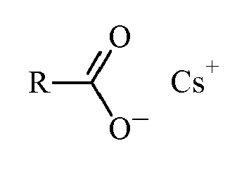

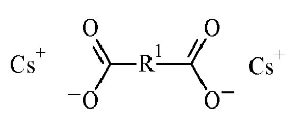


R1 für Alkylen (C2-C20 normal, verzweigt, gesättigt oder ungesättigt sowie hydroxysubstituiert), 1,2-Phenylen, 1,3-Phenylen 1,4-Phenylen oder 2,6-Pyridylen steht,
n und m für beliebige kommerziell erhältliche Polymerisationsgrade der Prekursormaterialien steht, umfasst. - Bauelement nach Anspruch 1 oder 2, wobei die Zwischenschicht/das Interface, in der das Cäsiumsalz enthalten ist, lösungsprozessiert aufgebracht ist.
- Bauelement nach einem der vorgenannten Ansprüche, wobei die Zwischenschicht/das Interface, in der das Cäsiumsalz enthalten ist, aufgedampft ist.
- Bauelement nach einem der vorgenannten Ansprüche, wobei die Zwischenschicht/das Interface, in der das Cäsiumsalz enthalten ist, eine Dicke im Bereich zwischen 0,1 nm und 15 nm hat.
Applications Claiming Priority (1)
| Application Number | Priority Date | Filing Date | Title |
|---|---|---|---|
| DE102007045518A DE102007045518B4 (de) | 2007-09-24 | 2007-09-24 | Lösungsprozessiertes organisches elektronisches Bauelement mit verbesserter Elektrodenschicht |
Publications (3)
| Publication Number | Publication Date |
|---|---|
| EP2040317A2 true EP2040317A2 (de) | 2009-03-25 |
| EP2040317A3 EP2040317A3 (de) | 2011-09-14 |
| EP2040317B1 EP2040317B1 (de) | 2018-04-04 |
Family
ID=39865506
Family Applications (1)
| Application Number | Title | Priority Date | Filing Date |
|---|---|---|---|
| EP08164755.4A Not-in-force EP2040317B1 (de) | 2007-09-24 | 2008-09-22 | Lösungsprozessiertes organisches elektronisches Bauelement mit verbesserter Elektrodenschicht |
Country Status (4)
| Country | Link |
|---|---|
| US (2) | US20090085472A1 (de) |
| EP (1) | EP2040317B1 (de) |
| JP (1) | JP5692959B2 (de) |
| DE (1) | DE102007045518B4 (de) |
Cited By (2)
| Publication number | Priority date | Publication date | Assignee | Title |
|---|---|---|---|---|
| US10032983B2 (en) | 2013-05-27 | 2018-07-24 | Merck Patent Gmbh | Electron transfer composition for use in an electron injection layer for organic electronic devices |
| CN112390908A (zh) * | 2019-08-12 | 2021-02-23 | 中国石油化工股份有限公司 | 聚合物悬浮液及其制备方法和应用 |
Families Citing this family (2)
| Publication number | Priority date | Publication date | Assignee | Title |
|---|---|---|---|---|
| KR101421559B1 (ko) | 2010-01-20 | 2014-07-23 | 경북대학교 산학협력단 | 도핑된 유기반도체를 포함하는 유기소자 |
| CN103779498A (zh) * | 2014-01-23 | 2014-05-07 | 上海交通大学 | 一种导电高分子材料的电子注入方法 |
Family Cites Families (20)
| Publication number | Priority date | Publication date | Assignee | Title |
|---|---|---|---|---|
| US4895674A (en) * | 1987-03-16 | 1990-01-23 | King Industries, Inc. | Thermally stable sulfonate compositions |
| JP2851517B2 (ja) * | 1993-09-28 | 1999-01-27 | 帝人株式会社 | 芳香族ジカルボン酸ジアリールエステルの製造方法 |
| US5965281A (en) * | 1997-02-04 | 1999-10-12 | Uniax Corporation | Electrically active polymer compositions and their use in efficient, low operating voltage, polymer light-emitting diodes with air-stable cathodes |
| US6114088A (en) * | 1999-01-15 | 2000-09-05 | 3M Innovative Properties Company | Thermal transfer element for forming multilayer devices |
| JP2001265251A (ja) * | 2000-03-17 | 2001-09-28 | Minolta Co Ltd | 表示素子及び積層型表示素子 |
| KR100507346B1 (ko) * | 2000-12-25 | 2005-08-08 | 삼성에스디아이 주식회사 | 유기 전기발광 소자 |
| SG118077A1 (en) * | 2001-06-21 | 2006-01-27 | Univ Singapore | Light emitting polymers and polymer light emittingdiodes |
| JP4207441B2 (ja) * | 2002-03-18 | 2009-01-14 | セイコーエプソン株式会社 | 有機el素子の製造方法 |
| JP2003303681A (ja) * | 2002-04-09 | 2003-10-24 | Sharp Corp | 有機led素子およびその製造方法、有機led表示装置 |
| US6797129B2 (en) | 2002-06-03 | 2004-09-28 | Eastman Kodak Company | Organic light-emitting device structure using metal cathode sputtering |
| US20030224204A1 (en) * | 2002-06-03 | 2003-12-04 | Eastman Kodak Company | Sputtered cathode for an organic light-emitting device having an alkali metal compound in the device structure |
| DE10261609B4 (de) * | 2002-12-20 | 2007-05-03 | Novaled Ag | Lichtemittierende Anordnung |
| JP4366106B2 (ja) * | 2003-04-30 | 2009-11-18 | キヤノン株式会社 | 発光素子 |
| DE102004010954A1 (de) | 2004-03-03 | 2005-10-06 | Novaled Gmbh | Verwendung eines Metallkomplexes als n-Dotand für ein organisches halbleitendes Matrixmaterial, organisches Halbleitermaterial und elektronisches Bauteil |
| JP2005259523A (ja) * | 2004-03-11 | 2005-09-22 | Idemitsu Kosan Co Ltd | 有機エレクトロルミネッセンス素子、その製造方法及び有機溶液 |
| EP1648042B1 (de) * | 2004-10-07 | 2007-05-02 | Novaled AG | Verfahren zur Dotierung von einem Halbleitermaterial mit Cäsium |
| JP2007059243A (ja) | 2005-08-25 | 2007-03-08 | Konica Minolta Holdings Inc | 有機エレクトロルミネッセンス素子、表示装置及び照明装置 |
| JP5050333B2 (ja) * | 2005-09-20 | 2012-10-17 | コニカミノルタホールディングス株式会社 | 有機エレクトロルミネッセンス素子 |
| WO2007069539A1 (ja) * | 2005-12-15 | 2007-06-21 | Konica Minolta Holdings, Inc. | 有機エレクトロルミネッセンス素子、表示装置および照明装置 |
| FR2892860A1 (fr) * | 2006-02-28 | 2007-05-04 | Thomson Licensing Sas | Diode organique a couche dopee n ou p comprenant un agent complexant du dopant |
-
2007
- 2007-09-24 DE DE102007045518A patent/DE102007045518B4/de not_active Expired - Fee Related
-
2008
- 2008-09-19 JP JP2008240682A patent/JP5692959B2/ja not_active Expired - Fee Related
- 2008-09-22 US US12/234,903 patent/US20090085472A1/en not_active Abandoned
- 2008-09-22 EP EP08164755.4A patent/EP2040317B1/de not_active Not-in-force
-
2012
- 2012-05-09 US US13/467,594 patent/US9040112B2/en not_active Expired - Fee Related
Cited By (3)
| Publication number | Priority date | Publication date | Assignee | Title |
|---|---|---|---|---|
| US10032983B2 (en) | 2013-05-27 | 2018-07-24 | Merck Patent Gmbh | Electron transfer composition for use in an electron injection layer for organic electronic devices |
| CN112390908A (zh) * | 2019-08-12 | 2021-02-23 | 中国石油化工股份有限公司 | 聚合物悬浮液及其制备方法和应用 |
| CN112390908B (zh) * | 2019-08-12 | 2022-07-12 | 中国石油化工股份有限公司 | 聚合物悬浮液及其制备方法和应用 |
Also Published As
| Publication number | Publication date |
|---|---|
| US20090085472A1 (en) | 2009-04-02 |
| US20120220075A1 (en) | 2012-08-30 |
| JP5692959B2 (ja) | 2015-04-01 |
| US9040112B2 (en) | 2015-05-26 |
| DE102007045518A1 (de) | 2009-04-02 |
| EP2040317B1 (de) | 2018-04-04 |
| JP2009076461A (ja) | 2009-04-09 |
| DE102007045518B4 (de) | 2010-12-16 |
| EP2040317A3 (de) | 2011-09-14 |
Similar Documents
| Publication | Publication Date | Title |
|---|---|---|
| EP1798785B1 (de) | Transparente polymere Elektrode für elektro-optische Aufbauten | |
| EP1227529B1 (de) | Elektrolumineszierende Anordnungen | |
| EP1564251B1 (de) | Polythiophenformulierungen zur Verbesserung von organischen Leuchtdioden | |
| EP1810986B1 (de) | Polythiophenformulierungen zur Verbesserung von organischen Leuchtdioden | |
| EP0991303B1 (de) | Hilfsschichten für elektrolumineszierende Anordnungen | |
| EP1505664B1 (de) | Transparente Elektrode für elektro-optische Aufbauten | |
| EP1564250B1 (de) | Polythiophenformulierungen zur Verbesserung von organischen Leuchtdioden | |
| DE112011105265B4 (de) | Organisches elektronisches Bauelement und Verfahren zu dessen Herstellung | |
| EP0909464B1 (de) | Elektrolumineszierende anordnungen | |
| EP1307498B1 (de) | Strukturierbare materialien, verfahren zu deren herstellung und deren verwendung | |
| DE69535080T2 (de) | Polymere für optische Vorrichtungen | |
| DE102011052509B4 (de) | Wasser-Aufnahmemittel und eine organoelektrische Vorrichtung, die das Wasser-Aufnahmemittel darin enthält | |
| EP1162238A2 (de) | Zusammensetzungen aus Polythiophen und Lösemittel | |
| EP2040317B1 (de) | Lösungsprozessiertes organisches elektronisches Bauelement mit verbesserter Elektrodenschicht | |
| DE102010012180A1 (de) | Sulfonierte Polyketone als Gegenion leitfähiger Polymere | |
| EP2092041B9 (de) | Neuartiges hochleitfähiges organisches ladungsträgertransportmaterial | |
| DE10261609A1 (de) | Lichtemittierende Anordnung | |
| DE102004010811B4 (de) | Polythiophenformulierungen zur Verbesserung von organischen Leuchtdioden | |
| WO2009056462A1 (de) | Verfahren zur beschichtung von unpolaren polyaromaten enthaltenden schichten | |
| DE60023001T2 (de) | Leitende polymere | |
| DE102011018480A1 (de) | Fluorierte Amine als SAM in OLEDs |
Legal Events
| Date | Code | Title | Description |
|---|---|---|---|
| PUAI | Public reference made under article 153(3) epc to a published international application that has entered the european phase |
Free format text: ORIGINAL CODE: 0009012 |
|
| AK | Designated contracting states |
Kind code of ref document: A2 Designated state(s): AT BE BG CH CY CZ DE DK EE ES FI FR GB GR HR HU IE IS IT LI LT LU LV MC MT NL NO PL PT RO SE SI SK TR |
|
| AX | Request for extension of the european patent |
Extension state: AL BA MK RS |
|
| PUAL | Search report despatched |
Free format text: ORIGINAL CODE: 0009013 |
|
| AK | Designated contracting states |
Kind code of ref document: A3 Designated state(s): AT BE BG CH CY CZ DE DK EE ES FI FR GB GR HR HU IE IS IT LI LT LU LV MC MT NL NO PL PT RO SE SI SK TR |
|
| AX | Request for extension of the european patent |
Extension state: AL BA MK RS |
|
| RIC1 | Information provided on ipc code assigned before grant |
Ipc: H01L 51/52 20060101AFI20110811BHEP |
|
| 17P | Request for examination filed |
Effective date: 20111021 |
|
| AKX | Designation fees paid |
Designated state(s): AT BE BG CH CY CZ DE DK EE ES FI FR GB GR HR HU IE IS IT LI LT LU LV MC MT NL NO PL PT RO SE SI SK TR |
|
| 17Q | First examination report despatched |
Effective date: 20121205 |
|
| RAP1 | Party data changed (applicant data changed or rights of an application transferred) |
Owner name: OSRAM OPTO SEMICONDUCTORS GMBH Owner name: SIEMENS AKTIENGESELLSCHAFT |
|
| STAA | Information on the status of an ep patent application or granted ep patent |
Free format text: STATUS: EXAMINATION IS IN PROGRESS |
|
| REG | Reference to a national code |
Ref country code: DE Ref legal event code: R079 Ref document number: 502008016003 Country of ref document: DE Free format text: PREVIOUS MAIN CLASS: H01L0051520000 Ipc: H01L0051540000 |
|
| RIC1 | Information provided on ipc code assigned before grant |
Ipc: H01L 51/50 20060101AFI20170707BHEP |
|
| RIC1 | Information provided on ipc code assigned before grant |
Ipc: H01L 51/54 20060101AFI20170720BHEP |
|
| RAP1 | Party data changed (applicant data changed or rights of an application transferred) |
Owner name: OSRAM OPTO SEMICONDUCTORS GMBH Owner name: SIEMENS AKTIENGESELLSCHAFT |
|
| GRAP | Despatch of communication of intention to grant a patent |
Free format text: ORIGINAL CODE: EPIDOSNIGR1 |
|
| STAA | Information on the status of an ep patent application or granted ep patent |
Free format text: STATUS: GRANT OF PATENT IS INTENDED |
|
| INTG | Intention to grant announced |
Effective date: 20171025 |
|
| RAP1 | Party data changed (applicant data changed or rights of an application transferred) |
Owner name: OSRAM OLED GMBH Owner name: SIEMENS AKTIENGESELLSCHAFT |
|
| GRAS | Grant fee paid |
Free format text: ORIGINAL CODE: EPIDOSNIGR3 |
|
| GRAA | (expected) grant |
Free format text: ORIGINAL CODE: 0009210 |
|
| STAA | Information on the status of an ep patent application or granted ep patent |
Free format text: STATUS: THE PATENT HAS BEEN GRANTED |
|
| AK | Designated contracting states |
Kind code of ref document: B1 Designated state(s): AT BE BG CH CY CZ DE DK EE ES FI FR GB GR HR HU IE IS IT LI LT LU LV MC MT NL NO PL PT RO SE SI SK TR |
|
| REG | Reference to a national code |
Ref country code: GB Ref legal event code: FG4D Free format text: NOT ENGLISH |
|
| REG | Reference to a national code |
Ref country code: CH Ref legal event code: EP |
|
| REG | Reference to a national code |
Ref country code: AT Ref legal event code: REF Ref document number: 986503 Country of ref document: AT Kind code of ref document: T Effective date: 20180415 |
|
| REG | Reference to a national code |
Ref country code: DE Ref legal event code: R096 Ref document number: 502008016003 Country of ref document: DE |
|
| REG | Reference to a national code |
Ref country code: IE Ref legal event code: FG4D Free format text: LANGUAGE OF EP DOCUMENT: GERMAN |
|
| REG | Reference to a national code |
Ref country code: NL Ref legal event code: MP Effective date: 20180404 |
|
| REG | Reference to a national code |
Ref country code: LT Ref legal event code: MG4D |
|
| PG25 | Lapsed in a contracting state [announced via postgrant information from national office to epo] |
Ref country code: NL Free format text: LAPSE BECAUSE OF FAILURE TO SUBMIT A TRANSLATION OF THE DESCRIPTION OR TO PAY THE FEE WITHIN THE PRESCRIBED TIME-LIMIT Effective date: 20180404 |
|
| PG25 | Lapsed in a contracting state [announced via postgrant information from national office to epo] |
Ref country code: FI Free format text: LAPSE BECAUSE OF FAILURE TO SUBMIT A TRANSLATION OF THE DESCRIPTION OR TO PAY THE FEE WITHIN THE PRESCRIBED TIME-LIMIT Effective date: 20180404 Ref country code: NO Free format text: LAPSE BECAUSE OF FAILURE TO SUBMIT A TRANSLATION OF THE DESCRIPTION OR TO PAY THE FEE WITHIN THE PRESCRIBED TIME-LIMIT Effective date: 20180704 Ref country code: BG Free format text: LAPSE BECAUSE OF FAILURE TO SUBMIT A TRANSLATION OF THE DESCRIPTION OR TO PAY THE FEE WITHIN THE PRESCRIBED TIME-LIMIT Effective date: 20180704 Ref country code: ES Free format text: LAPSE BECAUSE OF FAILURE TO SUBMIT A TRANSLATION OF THE DESCRIPTION OR TO PAY THE FEE WITHIN THE PRESCRIBED TIME-LIMIT Effective date: 20180404 Ref country code: SE Free format text: LAPSE BECAUSE OF FAILURE TO SUBMIT A TRANSLATION OF THE DESCRIPTION OR TO PAY THE FEE WITHIN THE PRESCRIBED TIME-LIMIT Effective date: 20180404 Ref country code: PL Free format text: LAPSE BECAUSE OF FAILURE TO SUBMIT A TRANSLATION OF THE DESCRIPTION OR TO PAY THE FEE WITHIN THE PRESCRIBED TIME-LIMIT Effective date: 20180404 Ref country code: LT Free format text: LAPSE BECAUSE OF FAILURE TO SUBMIT A TRANSLATION OF THE DESCRIPTION OR TO PAY THE FEE WITHIN THE PRESCRIBED TIME-LIMIT Effective date: 20180404 |
|
| PG25 | Lapsed in a contracting state [announced via postgrant information from national office to epo] |
Ref country code: LV Free format text: LAPSE BECAUSE OF FAILURE TO SUBMIT A TRANSLATION OF THE DESCRIPTION OR TO PAY THE FEE WITHIN THE PRESCRIBED TIME-LIMIT Effective date: 20180404 Ref country code: HR Free format text: LAPSE BECAUSE OF FAILURE TO SUBMIT A TRANSLATION OF THE DESCRIPTION OR TO PAY THE FEE WITHIN THE PRESCRIBED TIME-LIMIT Effective date: 20180404 Ref country code: GR Free format text: LAPSE BECAUSE OF FAILURE TO SUBMIT A TRANSLATION OF THE DESCRIPTION OR TO PAY THE FEE WITHIN THE PRESCRIBED TIME-LIMIT Effective date: 20180705 |
|
| PG25 | Lapsed in a contracting state [announced via postgrant information from national office to epo] |
Ref country code: PT Free format text: LAPSE BECAUSE OF FAILURE TO SUBMIT A TRANSLATION OF THE DESCRIPTION OR TO PAY THE FEE WITHIN THE PRESCRIBED TIME-LIMIT Effective date: 20180806 |
|
| REG | Reference to a national code |
Ref country code: DE Ref legal event code: R097 Ref document number: 502008016003 Country of ref document: DE |
|
| PG25 | Lapsed in a contracting state [announced via postgrant information from national office to epo] |
Ref country code: DK Free format text: LAPSE BECAUSE OF FAILURE TO SUBMIT A TRANSLATION OF THE DESCRIPTION OR TO PAY THE FEE WITHIN THE PRESCRIBED TIME-LIMIT Effective date: 20180404 Ref country code: EE Free format text: LAPSE BECAUSE OF FAILURE TO SUBMIT A TRANSLATION OF THE DESCRIPTION OR TO PAY THE FEE WITHIN THE PRESCRIBED TIME-LIMIT Effective date: 20180404 Ref country code: RO Free format text: LAPSE BECAUSE OF FAILURE TO SUBMIT A TRANSLATION OF THE DESCRIPTION OR TO PAY THE FEE WITHIN THE PRESCRIBED TIME-LIMIT Effective date: 20180404 Ref country code: CZ Free format text: LAPSE BECAUSE OF FAILURE TO SUBMIT A TRANSLATION OF THE DESCRIPTION OR TO PAY THE FEE WITHIN THE PRESCRIBED TIME-LIMIT Effective date: 20180404 Ref country code: SK Free format text: LAPSE BECAUSE OF FAILURE TO SUBMIT A TRANSLATION OF THE DESCRIPTION OR TO PAY THE FEE WITHIN THE PRESCRIBED TIME-LIMIT Effective date: 20180404 |
|
| PLBE | No opposition filed within time limit |
Free format text: ORIGINAL CODE: 0009261 |
|
| STAA | Information on the status of an ep patent application or granted ep patent |
Free format text: STATUS: NO OPPOSITION FILED WITHIN TIME LIMIT |
|
| PG25 | Lapsed in a contracting state [announced via postgrant information from national office to epo] |
Ref country code: IT Free format text: LAPSE BECAUSE OF FAILURE TO SUBMIT A TRANSLATION OF THE DESCRIPTION OR TO PAY THE FEE WITHIN THE PRESCRIBED TIME-LIMIT Effective date: 20180404 |
|
| 26N | No opposition filed |
Effective date: 20190107 |
|
| PG25 | Lapsed in a contracting state [announced via postgrant information from national office to epo] |
Ref country code: MC Free format text: LAPSE BECAUSE OF FAILURE TO SUBMIT A TRANSLATION OF THE DESCRIPTION OR TO PAY THE FEE WITHIN THE PRESCRIBED TIME-LIMIT Effective date: 20180404 |
|
| REG | Reference to a national code |
Ref country code: CH Ref legal event code: PL |
|
| GBPC | Gb: european patent ceased through non-payment of renewal fee |
Effective date: 20180922 |
|
| PG25 | Lapsed in a contracting state [announced via postgrant information from national office to epo] |
Ref country code: SI Free format text: LAPSE BECAUSE OF FAILURE TO SUBMIT A TRANSLATION OF THE DESCRIPTION OR TO PAY THE FEE WITHIN THE PRESCRIBED TIME-LIMIT Effective date: 20180404 |
|
| REG | Reference to a national code |
Ref country code: BE Ref legal event code: MM Effective date: 20180930 |
|
| REG | Reference to a national code |
Ref country code: IE Ref legal event code: MM4A |
|
| PG25 | Lapsed in a contracting state [announced via postgrant information from national office to epo] |
Ref country code: LU Free format text: LAPSE BECAUSE OF NON-PAYMENT OF DUE FEES Effective date: 20180922 |
|
| PG25 | Lapsed in a contracting state [announced via postgrant information from national office to epo] |
Ref country code: IE Free format text: LAPSE BECAUSE OF NON-PAYMENT OF DUE FEES Effective date: 20180922 |
|
| REG | Reference to a national code |
Ref country code: DE Ref legal event code: R082 Ref document number: 502008016003 Country of ref document: DE Representative=s name: EPPING HERMANN FISCHER PATENTANWALTSGESELLSCHA, DE Ref country code: DE Ref legal event code: R081 Ref document number: 502008016003 Country of ref document: DE Owner name: OSRAM OLED GMBH, DE Free format text: FORMER OWNERS: OSRAM OLED GMBH, 93049 REGENSBURG, DE; SIEMENS AKTIENGESELLSCHAFT, 80333 MUENCHEN, DE |
|
| PG25 | Lapsed in a contracting state [announced via postgrant information from national office to epo] |
Ref country code: FR Free format text: LAPSE BECAUSE OF NON-PAYMENT OF DUE FEES Effective date: 20180930 Ref country code: CH Free format text: LAPSE BECAUSE OF NON-PAYMENT OF DUE FEES Effective date: 20180930 Ref country code: LI Free format text: LAPSE BECAUSE OF NON-PAYMENT OF DUE FEES Effective date: 20180930 Ref country code: BE Free format text: LAPSE BECAUSE OF NON-PAYMENT OF DUE FEES Effective date: 20180930 |
|
| PG25 | Lapsed in a contracting state [announced via postgrant information from national office to epo] |
Ref country code: GB Free format text: LAPSE BECAUSE OF NON-PAYMENT OF DUE FEES Effective date: 20180922 |
|
| REG | Reference to a national code |
Ref country code: AT Ref legal event code: MM01 Ref document number: 986503 Country of ref document: AT Kind code of ref document: T Effective date: 20180922 |
|
| PG25 | Lapsed in a contracting state [announced via postgrant information from national office to epo] |
Ref country code: AT Free format text: LAPSE BECAUSE OF NON-PAYMENT OF DUE FEES Effective date: 20180922 Ref country code: MT Free format text: LAPSE BECAUSE OF FAILURE TO SUBMIT A TRANSLATION OF THE DESCRIPTION OR TO PAY THE FEE WITHIN THE PRESCRIBED TIME-LIMIT Effective date: 20180404 |
|
| PG25 | Lapsed in a contracting state [announced via postgrant information from national office to epo] |
Ref country code: TR Free format text: LAPSE BECAUSE OF FAILURE TO SUBMIT A TRANSLATION OF THE DESCRIPTION OR TO PAY THE FEE WITHIN THE PRESCRIBED TIME-LIMIT Effective date: 20180404 |
|
| PG25 | Lapsed in a contracting state [announced via postgrant information from national office to epo] |
Ref country code: HU Free format text: LAPSE BECAUSE OF FAILURE TO SUBMIT A TRANSLATION OF THE DESCRIPTION OR TO PAY THE FEE WITHIN THE PRESCRIBED TIME-LIMIT; INVALID AB INITIO Effective date: 20080922 |
|
| PG25 | Lapsed in a contracting state [announced via postgrant information from national office to epo] |
Ref country code: CY Free format text: LAPSE BECAUSE OF FAILURE TO SUBMIT A TRANSLATION OF THE DESCRIPTION OR TO PAY THE FEE WITHIN THE PRESCRIBED TIME-LIMIT Effective date: 20180404 |
|
| PG25 | Lapsed in a contracting state [announced via postgrant information from national office to epo] |
Ref country code: IS Free format text: LAPSE BECAUSE OF FAILURE TO SUBMIT A TRANSLATION OF THE DESCRIPTION OR TO PAY THE FEE WITHIN THE PRESCRIBED TIME-LIMIT Effective date: 20180804 |
|
| PGFP | Annual fee paid to national office [announced via postgrant information from national office to epo] |
Ref country code: DE Payment date: 20210924 Year of fee payment: 14 |
|
| REG | Reference to a national code |
Ref country code: DE Ref legal event code: R079 Ref document number: 502008016003 Country of ref document: DE Free format text: PREVIOUS MAIN CLASS: H01L0051540000 Ipc: H10K0085000000 |
|
| REG | Reference to a national code |
Ref country code: DE Ref legal event code: R119 Ref document number: 502008016003 Country of ref document: DE |
|
| PG25 | Lapsed in a contracting state [announced via postgrant information from national office to epo] |
Ref country code: DE Free format text: LAPSE BECAUSE OF NON-PAYMENT OF DUE FEES Effective date: 20230401 |