EP2040291B1 - Procédé de collage de puces sur un substrat de contrainte et procédé de mise sous contrainte d'un circuit de lecture semi-conducteur - Google Patents
Procédé de collage de puces sur un substrat de contrainte et procédé de mise sous contrainte d'un circuit de lecture semi-conducteur Download PDFInfo
- Publication number
- EP2040291B1 EP2040291B1 EP08164325.6A EP08164325A EP2040291B1 EP 2040291 B1 EP2040291 B1 EP 2040291B1 EP 08164325 A EP08164325 A EP 08164325A EP 2040291 B1 EP2040291 B1 EP 2040291B1
- Authority
- EP
- European Patent Office
- Prior art keywords
- substrate
- layers
- adhesive
- chips
- constraint
- Prior art date
- Legal status (The legal status is an assumption and is not a legal conclusion. Google has not performed a legal analysis and makes no representation as to the accuracy of the status listed.)
- Active
Links
Images

Classifications
-
- H—ELECTRICITY
- H10—SEMICONDUCTOR DEVICES; ELECTRIC SOLID-STATE DEVICES NOT OTHERWISE PROVIDED FOR
- H10P—GENERIC PROCESSES OR APPARATUS FOR THE MANUFACTURE OR TREATMENT OF DEVICES COVERED BY CLASS H10
- H10P72/00—Handling or holding of wafers, substrates or devices during manufacture or treatment thereof
- H10P72/70—Handling or holding of wafers, substrates or devices during manufacture or treatment thereof for supporting or gripping
- H10P72/74—Handling or holding of wafers, substrates or devices during manufacture or treatment thereof for supporting or gripping using temporarily an auxiliary support
-
- H—ELECTRICITY
- H10—SEMICONDUCTOR DEVICES; ELECTRIC SOLID-STATE DEVICES NOT OTHERWISE PROVIDED FOR
- H10F—INORGANIC SEMICONDUCTOR DEVICES SENSITIVE TO INFRARED RADIATION, LIGHT, ELECTROMAGNETIC RADIATION OF SHORTER WAVELENGTH OR CORPUSCULAR RADIATION
- H10F39/00—Integrated devices, or assemblies of multiple devices, comprising at least one element covered by group H10F30/00, e.g. radiation detectors comprising photodiode arrays
- H10F39/011—Manufacture or treatment of image sensors covered by group H10F39/12
- H10F39/018—Manufacture or treatment of image sensors covered by group H10F39/12 of hybrid image sensors
-
- H—ELECTRICITY
- H10—SEMICONDUCTOR DEVICES; ELECTRIC SOLID-STATE DEVICES NOT OTHERWISE PROVIDED FOR
- H10P—GENERIC PROCESSES OR APPARATUS FOR THE MANUFACTURE OR TREATMENT OF DEVICES COVERED BY CLASS H10
- H10P54/00—Cutting or separating of wafers, substrates or parts of devices
-
- H—ELECTRICITY
- H10—SEMICONDUCTOR DEVICES; ELECTRIC SOLID-STATE DEVICES NOT OTHERWISE PROVIDED FOR
- H10P—GENERIC PROCESSES OR APPARATUS FOR THE MANUFACTURE OR TREATMENT OF DEVICES COVERED BY CLASS H10
- H10P72/00—Handling or holding of wafers, substrates or devices during manufacture or treatment thereof
- H10P72/70—Handling or holding of wafers, substrates or devices during manufacture or treatment thereof for supporting or gripping
- H10P72/74—Handling or holding of wafers, substrates or devices during manufacture or treatment thereof for supporting or gripping using temporarily an auxiliary support
- H10P72/7428—Handling or holding of wafers, substrates or devices during manufacture or treatment thereof for supporting or gripping using temporarily an auxiliary support used to support diced chips prior to mounting
-
- H—ELECTRICITY
- H10—SEMICONDUCTOR DEVICES; ELECTRIC SOLID-STATE DEVICES NOT OTHERWISE PROVIDED FOR
- H10P—GENERIC PROCESSES OR APPARATUS FOR THE MANUFACTURE OR TREATMENT OF DEVICES COVERED BY CLASS H10
- H10P72/00—Handling or holding of wafers, substrates or devices during manufacture or treatment thereof
- H10P72/70—Handling or holding of wafers, substrates or devices during manufacture or treatment thereof for supporting or gripping
- H10P72/74—Handling or holding of wafers, substrates or devices during manufacture or treatment thereof for supporting or gripping using temporarily an auxiliary support
- H10P72/7438—Handling or holding of wafers, substrates or devices during manufacture or treatment thereof for supporting or gripping using temporarily an auxiliary support with parts of the auxiliary support remaining in the finished device
-
- H—ELECTRICITY
- H10—SEMICONDUCTOR DEVICES; ELECTRIC SOLID-STATE DEVICES NOT OTHERWISE PROVIDED FOR
- H10W—GENERIC PACKAGES, INTERCONNECTIONS, CONNECTORS OR OTHER CONSTRUCTIONAL DETAILS OF DEVICES COVERED BY CLASS H10
- H10W72/00—Interconnections or connectors in packages
- H10W72/01—Manufacture or treatment
- H10W72/0198—Manufacture or treatment batch processes
-
- H—ELECTRICITY
- H10—SEMICONDUCTOR DEVICES; ELECTRIC SOLID-STATE DEVICES NOT OTHERWISE PROVIDED FOR
- H10W—GENERIC PACKAGES, INTERCONNECTIONS, CONNECTORS OR OTHER CONSTRUCTIONAL DETAILS OF DEVICES COVERED BY CLASS H10
- H10W72/00—Interconnections or connectors in packages
- H10W72/071—Connecting or disconnecting
- H10W72/073—Connecting or disconnecting of die-attach connectors
- H10W72/07351—Connecting or disconnecting of die-attach connectors characterised by changes in properties of the die-attach connectors during connecting
- H10W72/07352—Connecting or disconnecting of die-attach connectors characterised by changes in properties of the die-attach connectors during connecting changes in structures or sizes
-
- H—ELECTRICITY
- H10—SEMICONDUCTOR DEVICES; ELECTRIC SOLID-STATE DEVICES NOT OTHERWISE PROVIDED FOR
- H10W—GENERIC PACKAGES, INTERCONNECTIONS, CONNECTORS OR OTHER CONSTRUCTIONAL DETAILS OF DEVICES COVERED BY CLASS H10
- H10W72/00—Interconnections or connectors in packages
- H10W72/30—Die-attach connectors
- H10W72/321—Structures or relative sizes of die-attach connectors
Definitions
- the invention relates to a method for bonding chips to a stress substrate and to a method for stressing a semiconductor readout circuit with a material of different expansion coefficient.
- thermomechanical reliability of heterogeneous assemblies that is to say constituted by two parts with different properties, for example different expansion coefficients or Young's moduli, requires the exploitation of a bimetallic structure, or even of a structure called BCS (Balanced Composite Structure).
- BCS Band-Chip Composite Structure
- Such structures are characterized by bonding a so-called stress substrate on the assembly to be reliable.
- the document referenced [1] at the end of the description thus describes a set of interconnections between a read circuit and a detection focal plane.
- This set as illustrated on the figure 1 , comprises a first radiation detection semiconductor layer 10 having a first coefficient of expansion, a second semiconductor electronic circuit multiplexing layer 12 having a second coefficient of expansion, a second third interconnection layer 13 located between the two first layers 10 and 12, and a strain substrate 14 having a large coefficient of expansion bonded to the lower surface of the second layer 12.
- This document describes a structure made reliable "from below” .
- the referenced document [2] describes a structure made reliable "from above". As illustrated on the figure 2 this structure comprises a radiation detection layer 20, a read layer 22 and an interconnection layer 23 located between these two first layers 20 and 22.
- the structures are characterized by the bonding of a stress substrate on the assembly to be reliable.
- the referenced document [3] describes a hybrid focal plane array structure.
- this structure comprises an incident radiation detection semiconductor layer 31, a multiplexing layer 32, and an interconnection layer 33 between these two layers 30 and 32.
- a stress substrate 34 having mechanical characteristics and geometric identical to those of the detection layer 30 is glued to the lower surface of the layer 32.
- An additional layer 35 having characteristics identical to those of the layer 32 serves to correct the curvature of the assembly generated by the bimetallic strip 32, 34. All these three layers 32, 34, 35, forming a BCS structure, makes it possible to make the l 'together. This structure is thus made reliable "from below".
- the object of the invention is a low-cost method which makes it possible to perform a collective bonding of individual chips to a common substrate, which is similar to a large surface bonding, exploiting all the advantages of a bonding. unitary small area.
- a collective collage of the chips on a constraint substrate is described in the document US 2002/048906 A1 (See Figures 14A-14D, 15A, 15B).
- the invention also relates to a method of stressing a semiconductor reading circuit, for example silicon, by a substrate of a different coefficient of expansion material implementing the above method.
- this material is chosen from among the following materials: germanium, sapphire, BeO.
- the method of the invention is a method of collectively bonding individual chips to a common substrate.
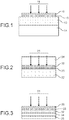
- layers 40 called “functionalized” or active that is to say integrating for example reading circuits, are arranged on a support 41, for example adhesive.
- these functionalized layers 40 have a surface structuring due for example to interconnect pads (for example solder balls) to subsequently interconnect the layers 40 to another circuit, the pads are directly in contact with the support adhesive 41.
- These functionalized layers 40 are arranged in an adjacent manner non-contiguous, with a spacing "e" between them of between 40 ⁇ m and 500 ⁇ m.
- a drop of calibrated adhesive 43 is then deposited on each of these functionalized layers.
- a stress substrate 44 is then transferred (arrow 47) to the assembly thus formed, which makes it possible to obtain the embodiment illustrated in FIG. figure 5 .
- Chips 45 are then singled out by cutting the stress substrate 44 as illustrated on FIG. figure 6 . These chips 45 are then detached from the support 41.
- the method of the invention combines the advantages of a "large surface” bonding, by the simultaneous treatment of several chips 45 by bonding a large stress substrate 44 on functionalized layers 40 pre-arranged on the support 41, with the advantages unitary bonding called "low surface” to prevent the appearance of bubbles.
- CdHgTe cooled infrared radiation
- CdTe X-ray radiation
- the method of the invention is applicable to any embodiment of a bimetallic strip (or of an assembly with more than two layers, as described in document referenced [3]) , intended to modify the thermomechanical behavior of a substrate, to adapt expansion coefficients.
- the method of the invention thus makes it possible to constrain any material to conform to the thermomechanical behavior of another material while respecting the rules of behavior of the bimetallic strips.
- the method of the invention can, more broadly, be applied to any multiple bonding of chips or materials on a base: for example, the transfer of optical chips (InP, GaAs, silica) on silicon assembly platforms (" silicon optical bench "), as described in the document referenced [4].
- optical chips InP, GaAs, silica
- silicon assembly platforms silicon optical bench "
- chips on bases GaN chips for lighting, silicon chips on ceramics or case backs, MCM or "Multi Chip Modules”
- encapsulation packaging
Landscapes
- Wire Bonding (AREA)
- Recrystallisation Techniques (AREA)
- Element Separation (AREA)
- Solid State Image Pick-Up Elements (AREA)
- Micromachines (AREA)
Applications Claiming Priority (1)
| Application Number | Priority Date | Filing Date | Title |
|---|---|---|---|
| FR0757676A FR2921201B1 (fr) | 2007-09-19 | 2007-09-19 | Procede de collage de puces sur un substrat de contrainte et procede de mise sous contrainte d'un circuit de lecture semi-conducteur |
Publications (2)
| Publication Number | Publication Date |
|---|---|
| EP2040291A1 EP2040291A1 (fr) | 2009-03-25 |
| EP2040291B1 true EP2040291B1 (fr) | 2018-03-14 |
Family
ID=39271531
Family Applications (1)
| Application Number | Title | Priority Date | Filing Date |
|---|---|---|---|
| EP08164325.6A Active EP2040291B1 (fr) | 2007-09-19 | 2008-09-15 | Procédé de collage de puces sur un substrat de contrainte et procédé de mise sous contrainte d'un circuit de lecture semi-conducteur |
Country Status (4)
| Country | Link |
|---|---|
| US (1) | US7645686B2 (https=) |
| EP (1) | EP2040291B1 (https=) |
| JP (1) | JP5557436B2 (https=) |
| FR (1) | FR2921201B1 (https=) |
Families Citing this family (2)
| Publication number | Priority date | Publication date | Assignee | Title |
|---|---|---|---|---|
| FR2961519B1 (fr) | 2010-06-18 | 2012-07-06 | Commissariat Energie Atomique | Procede de collage calibre en epaisseur entre au moins deux substrats |
| US10374000B2 (en) | 2013-09-23 | 2019-08-06 | Teledyne Scientific & Imaging, Llc | Thermal-contraction matched hybrid device package |
Family Cites Families (16)
| Publication number | Priority date | Publication date | Assignee | Title |
|---|---|---|---|---|
| US5365088A (en) | 1988-08-02 | 1994-11-15 | Santa Barbara Research Center | Thermal/mechanical buffer for HgCdTe/Si direct hybridization |
| JPH02271558A (ja) * | 1989-04-12 | 1990-11-06 | Mitsubishi Electric Corp | 半導体装置及びその製造方法 |
| US4943491A (en) * | 1989-11-20 | 1990-07-24 | Honeywell Inc. | Structure for improving interconnect reliability of focal plane arrays |
| JP2564694B2 (ja) * | 1990-09-10 | 1996-12-18 | ローム株式会社 | 半導体素子の製造方法 |
| EP0829907A1 (en) | 1996-09-16 | 1998-03-18 | Rockwell International Corporation | Hybrid focal plane array comprising stabilizing structure |
| JP3410371B2 (ja) * | 1998-08-18 | 2003-05-26 | リンテック株式会社 | ウエハ裏面研削時の表面保護シートおよびその利用方法 |
| US6255140B1 (en) * | 1998-10-19 | 2001-07-03 | Industrial Technology Research Institute | Flip chip chip-scale package |
| FR2810454B1 (fr) * | 2000-06-15 | 2003-07-18 | Sofradir | Detecteur de rayonnements electromagnetiques, et notamment de rayonnements infrarouges, et procede pour la realisation d'un tel detecteur |
| US6407381B1 (en) * | 2000-07-05 | 2002-06-18 | Amkor Technology, Inc. | Wafer scale image sensor package |
| JP3719921B2 (ja) * | 2000-09-29 | 2005-11-24 | 株式会社東芝 | 半導体装置及びその製造方法 |
| TW522531B (en) * | 2000-10-20 | 2003-03-01 | Matsushita Electric Industrial Co Ltd | Semiconductor device, method of manufacturing the device and mehtod of mounting the device |
| JP5022552B2 (ja) * | 2002-09-26 | 2012-09-12 | セイコーエプソン株式会社 | 電気光学装置の製造方法及び電気光学装置 |
| FR2857508B1 (fr) * | 2003-07-09 | 2005-09-09 | Fr De Detecteurs Infrarouges S | Procede pour la realisation d'un detecteur de rayonnements electromagnetiques, et notamment de rayonnements infrarouges, et detecteur ontenu au moyen de ce procede |
| JP4396472B2 (ja) * | 2004-10-06 | 2010-01-13 | パナソニック株式会社 | 薄膜状素子の転写方法 |
| JP4745073B2 (ja) * | 2006-02-03 | 2011-08-10 | シチズン電子株式会社 | 表面実装型発光素子の製造方法 |
| TWI463580B (zh) * | 2007-06-19 | 2014-12-01 | 瑞薩科技股份有限公司 | Manufacturing method of semiconductor integrated circuit device |
-
2007
- 2007-09-19 FR FR0757676A patent/FR2921201B1/fr not_active Expired - Fee Related
-
2008
- 2008-09-15 EP EP08164325.6A patent/EP2040291B1/fr active Active
- 2008-09-17 US US12/212,302 patent/US7645686B2/en active Active
- 2008-09-19 JP JP2008241065A patent/JP5557436B2/ja active Active
Non-Patent Citations (1)
| Title |
|---|
| None * |
Also Published As
| Publication number | Publication date |
|---|---|
| FR2921201B1 (fr) | 2009-12-18 |
| US7645686B2 (en) | 2010-01-12 |
| EP2040291A1 (fr) | 2009-03-25 |
| FR2921201A1 (fr) | 2009-03-20 |
| US20090075423A1 (en) | 2009-03-19 |
| JP2009076915A (ja) | 2009-04-09 |
| JP5557436B2 (ja) | 2014-07-23 |
Similar Documents
| Publication | Publication Date | Title |
|---|---|---|
| EP2279524B1 (fr) | Procede de realisation d'un dispositif optique a composants optoelectroniques integres | |
| EP2960937B1 (fr) | Circuit integre comportant un dissipateur de chaleur | |
| FR2704690A1 (fr) | Procédé d'encapsulation de pastilles semi-conductrices, dispositif obtenu par ce procédé et application à l'interconnexion de pastilles en trois dimensions. | |
| FR2917234A1 (fr) | Dispositif multi composants integres dans une matrice semi-conductrice. | |
| EP0662721B1 (fr) | Détecteur de rayonnement électromagnétique et procédé de fabrication | |
| FR3007403A1 (fr) | Procede de realisation d'un dispositif microelectronique mecaniquement autonome | |
| WO2021099713A1 (fr) | Procede de fabrication d'une puce fonctionnelle adaptee pour etre assemblee a des elements filaires | |
| FR2910707A1 (fr) | Capteur d'image a haute densite d'integration | |
| EP3089211B1 (fr) | Procede d'encapsulation d'un circuit electronique | |
| EP2040291B1 (fr) | Procédé de collage de puces sur un substrat de contrainte et procédé de mise sous contrainte d'un circuit de lecture semi-conducteur | |
| EP3809467B1 (fr) | Procédé de mise en courbure collective d'un ensemble de puces eléctroniques | |
| FR2961519A1 (fr) | Procede de collage calibre en epaisseur entre au moins deux substrats | |
| FR3098646A1 (fr) | Composant electronique resistant a l'humidite et procede de realisation d'un tel composant | |
| WO2018073517A1 (fr) | Procede de realisation d'une puce microelectronique destinee a etre hybridee a une deuxieme puce | |
| EP3031775B1 (fr) | Procede de realisation d'une connexion electrique dans un via borgne | |
| EP4531519B1 (fr) | Dispositif optoélectronique et son procédé de fabrication | |
| FR2809533A1 (fr) | Microsysteme monolithique a mosaique de composants | |
| EP2246890B1 (fr) | Mode de réalisation d'un module de capture d'images | |
| FR3140985A1 (fr) | Dispositif electronique de type sip et procede de realisation d’un tel dispositif | |
| EP1210690B1 (fr) | Dispositif electronique comportant au moins une puce fixee sur un support et procede de fabrication d'un tel dispositif | |
| EP2463909A2 (fr) | Procédé de fabrication de dispositifs semi-conducteurs et dispositifs semi-conducteurs | |
| EP4709136A1 (fr) | Procede de fabrication d'un assemblage 3d | |
| FR3094141A1 (fr) | procede de fabrication d’un composant optoelectronique a transmission optique en face arriere | |
| EP1359617A1 (fr) | Procédé de fabrication de modules électroniques | |
| FR2703828A1 (fr) | Nouvel assemblage de circuits intégrés à dissipateur thermique. |
Legal Events
| Date | Code | Title | Description |
|---|---|---|---|
| PUAI | Public reference made under article 153(3) epc to a published international application that has entered the european phase |
Free format text: ORIGINAL CODE: 0009012 |
|
| AK | Designated contracting states |
Kind code of ref document: A1 Designated state(s): AT BE BG CH CY CZ DE DK EE ES FI FR GB GR HR HU IE IS IT LI LT LU LV MC MT NL NO PL PT RO SE SI SK TR |
|
| AX | Request for extension of the european patent |
Extension state: AL BA MK RS |
|
| 17P | Request for examination filed |
Effective date: 20090427 |
|
| AKX | Designation fees paid |
Designated state(s): AT BE BG CH CY CZ DE DK EE ES FI FR GB GR HR HU IE IS IT LI LT LU LV MC MT NL NO PL PT RO SE SI SK TR |
|
| RAP1 | Party data changed (applicant data changed or rights of an application transferred) |
Owner name: COMMISSARIAT A L'ENERGIE ATOMIQUE ET AUX ENERGIES |
|
| STAA | Information on the status of an ep patent application or granted ep patent |
Free format text: STATUS: EXAMINATION IS IN PROGRESS |
|
| 17Q | First examination report despatched |
Effective date: 20170116 |
|
| RIC1 | Information provided on ipc code assigned before grant |
Ipc: H01L 21/58 20060101AFI20170803BHEP Ipc: H01L 21/683 20060101ALN20170803BHEP Ipc: H01L 27/146 20060101ALI20170803BHEP Ipc: H01L 31/024 20140101ALN20170803BHEP Ipc: H01L 21/78 20060101ALN20170803BHEP Ipc: H01L 23/34 20060101ALN20170803BHEP |
|
| REG | Reference to a national code |
Ref country code: DE Ref legal event code: R079 Ref document number: 602008054418 Country of ref document: DE Free format text: PREVIOUS MAIN CLASS: H01L0021680000 Ipc: H01L0021580000 |
|
| GRAP | Despatch of communication of intention to grant a patent |
Free format text: ORIGINAL CODE: EPIDOSNIGR1 |
|
| STAA | Information on the status of an ep patent application or granted ep patent |
Free format text: STATUS: GRANT OF PATENT IS INTENDED |
|
| RIC1 | Information provided on ipc code assigned before grant |
Ipc: H01L 21/78 20060101ALN20170911BHEP Ipc: H01L 31/024 20140101ALN20170911BHEP Ipc: H01L 27/146 20060101ALI20170911BHEP Ipc: H01L 23/34 20060101ALN20170911BHEP Ipc: H01L 21/58 20060101AFI20170911BHEP Ipc: H01L 21/683 20060101ALN20170911BHEP |
|
| INTG | Intention to grant announced |
Effective date: 20171005 |
|
| GRAS | Grant fee paid |
Free format text: ORIGINAL CODE: EPIDOSNIGR3 |
|
| GRAA | (expected) grant |
Free format text: ORIGINAL CODE: 0009210 |
|
| STAA | Information on the status of an ep patent application or granted ep patent |
Free format text: STATUS: THE PATENT HAS BEEN GRANTED |
|
| AK | Designated contracting states |
Kind code of ref document: B1 Designated state(s): AT BE BG CH CY CZ DE DK EE ES FI FR GB GR HR HU IE IS IT LI LT LU LV MC MT NL NO PL PT RO SE SI SK TR |
|
| REG | Reference to a national code |
Ref country code: GB Ref legal event code: FG4D Free format text: NOT ENGLISH |
|
| REG | Reference to a national code |
Ref country code: CH Ref legal event code: EP Ref country code: AT Ref legal event code: REF Ref document number: 979633 Country of ref document: AT Kind code of ref document: T Effective date: 20180315 |
|
| REG | Reference to a national code |
Ref country code: IE Ref legal event code: FG4D Free format text: LANGUAGE OF EP DOCUMENT: FRENCH |
|
| REG | Reference to a national code |
Ref country code: DE Ref legal event code: R096 Ref document number: 602008054418 Country of ref document: DE |
|
| REG | Reference to a national code |
Ref country code: NL Ref legal event code: MP Effective date: 20180314 |
|
| REG | Reference to a national code |
Ref country code: LT Ref legal event code: MG4D |
|
| PG25 | Lapsed in a contracting state [announced via postgrant information from national office to epo] |
Ref country code: LT Free format text: LAPSE BECAUSE OF FAILURE TO SUBMIT A TRANSLATION OF THE DESCRIPTION OR TO PAY THE FEE WITHIN THE PRESCRIBED TIME-LIMIT Effective date: 20180314 Ref country code: CY Free format text: LAPSE BECAUSE OF FAILURE TO SUBMIT A TRANSLATION OF THE DESCRIPTION OR TO PAY THE FEE WITHIN THE PRESCRIBED TIME-LIMIT Effective date: 20180314 Ref country code: HR Free format text: LAPSE BECAUSE OF FAILURE TO SUBMIT A TRANSLATION OF THE DESCRIPTION OR TO PAY THE FEE WITHIN THE PRESCRIBED TIME-LIMIT Effective date: 20180314 Ref country code: NO Free format text: LAPSE BECAUSE OF FAILURE TO SUBMIT A TRANSLATION OF THE DESCRIPTION OR TO PAY THE FEE WITHIN THE PRESCRIBED TIME-LIMIT Effective date: 20180614 Ref country code: FI Free format text: LAPSE BECAUSE OF FAILURE TO SUBMIT A TRANSLATION OF THE DESCRIPTION OR TO PAY THE FEE WITHIN THE PRESCRIBED TIME-LIMIT Effective date: 20180314 Ref country code: ES Free format text: LAPSE BECAUSE OF FAILURE TO SUBMIT A TRANSLATION OF THE DESCRIPTION OR TO PAY THE FEE WITHIN THE PRESCRIBED TIME-LIMIT Effective date: 20180314 |
|
| REG | Reference to a national code |
Ref country code: AT Ref legal event code: MK05 Ref document number: 979633 Country of ref document: AT Kind code of ref document: T Effective date: 20180314 |
|
| PG25 | Lapsed in a contracting state [announced via postgrant information from national office to epo] |
Ref country code: GR Free format text: LAPSE BECAUSE OF FAILURE TO SUBMIT A TRANSLATION OF THE DESCRIPTION OR TO PAY THE FEE WITHIN THE PRESCRIBED TIME-LIMIT Effective date: 20180615 Ref country code: BG Free format text: LAPSE BECAUSE OF FAILURE TO SUBMIT A TRANSLATION OF THE DESCRIPTION OR TO PAY THE FEE WITHIN THE PRESCRIBED TIME-LIMIT Effective date: 20180614 Ref country code: LV Free format text: LAPSE BECAUSE OF FAILURE TO SUBMIT A TRANSLATION OF THE DESCRIPTION OR TO PAY THE FEE WITHIN THE PRESCRIBED TIME-LIMIT Effective date: 20180314 Ref country code: SE Free format text: LAPSE BECAUSE OF FAILURE TO SUBMIT A TRANSLATION OF THE DESCRIPTION OR TO PAY THE FEE WITHIN THE PRESCRIBED TIME-LIMIT Effective date: 20180314 |
|
| PG25 | Lapsed in a contracting state [announced via postgrant information from national office to epo] |
Ref country code: MT Free format text: LAPSE BECAUSE OF FAILURE TO SUBMIT A TRANSLATION OF THE DESCRIPTION OR TO PAY THE FEE WITHIN THE PRESCRIBED TIME-LIMIT Effective date: 20180314 |
|
| REG | Reference to a national code |
Ref country code: FR Ref legal event code: PLFP Year of fee payment: 11 |
|
| PG25 | Lapsed in a contracting state [announced via postgrant information from national office to epo] |
Ref country code: NL Free format text: LAPSE BECAUSE OF FAILURE TO SUBMIT A TRANSLATION OF THE DESCRIPTION OR TO PAY THE FEE WITHIN THE PRESCRIBED TIME-LIMIT Effective date: 20180314 Ref country code: IT Free format text: LAPSE BECAUSE OF FAILURE TO SUBMIT A TRANSLATION OF THE DESCRIPTION OR TO PAY THE FEE WITHIN THE PRESCRIBED TIME-LIMIT Effective date: 20180314 Ref country code: EE Free format text: LAPSE BECAUSE OF FAILURE TO SUBMIT A TRANSLATION OF THE DESCRIPTION OR TO PAY THE FEE WITHIN THE PRESCRIBED TIME-LIMIT Effective date: 20180314 Ref country code: RO Free format text: LAPSE BECAUSE OF FAILURE TO SUBMIT A TRANSLATION OF THE DESCRIPTION OR TO PAY THE FEE WITHIN THE PRESCRIBED TIME-LIMIT Effective date: 20180314 Ref country code: PL Free format text: LAPSE BECAUSE OF FAILURE TO SUBMIT A TRANSLATION OF THE DESCRIPTION OR TO PAY THE FEE WITHIN THE PRESCRIBED TIME-LIMIT Effective date: 20180314 |
|
| PG25 | Lapsed in a contracting state [announced via postgrant information from national office to epo] |
Ref country code: SK Free format text: LAPSE BECAUSE OF FAILURE TO SUBMIT A TRANSLATION OF THE DESCRIPTION OR TO PAY THE FEE WITHIN THE PRESCRIBED TIME-LIMIT Effective date: 20180314 Ref country code: CZ Free format text: LAPSE BECAUSE OF FAILURE TO SUBMIT A TRANSLATION OF THE DESCRIPTION OR TO PAY THE FEE WITHIN THE PRESCRIBED TIME-LIMIT Effective date: 20180314 Ref country code: AT Free format text: LAPSE BECAUSE OF FAILURE TO SUBMIT A TRANSLATION OF THE DESCRIPTION OR TO PAY THE FEE WITHIN THE PRESCRIBED TIME-LIMIT Effective date: 20180314 |
|
| REG | Reference to a national code |
Ref country code: DE Ref legal event code: R097 Ref document number: 602008054418 Country of ref document: DE |
|
| PG25 | Lapsed in a contracting state [announced via postgrant information from national office to epo] |
Ref country code: PT Free format text: LAPSE BECAUSE OF FAILURE TO SUBMIT A TRANSLATION OF THE DESCRIPTION OR TO PAY THE FEE WITHIN THE PRESCRIBED TIME-LIMIT Effective date: 20180716 |
|
| PLBE | No opposition filed within time limit |
Free format text: ORIGINAL CODE: 0009261 |
|
| STAA | Information on the status of an ep patent application or granted ep patent |
Free format text: STATUS: NO OPPOSITION FILED WITHIN TIME LIMIT |
|
| PG25 | Lapsed in a contracting state [announced via postgrant information from national office to epo] |
Ref country code: DK Free format text: LAPSE BECAUSE OF FAILURE TO SUBMIT A TRANSLATION OF THE DESCRIPTION OR TO PAY THE FEE WITHIN THE PRESCRIBED TIME-LIMIT Effective date: 20180314 |
|
| 26N | No opposition filed |
Effective date: 20181217 |
|
| PG25 | Lapsed in a contracting state [announced via postgrant information from national office to epo] |
Ref country code: SI Free format text: LAPSE BECAUSE OF FAILURE TO SUBMIT A TRANSLATION OF THE DESCRIPTION OR TO PAY THE FEE WITHIN THE PRESCRIBED TIME-LIMIT Effective date: 20180314 |
|
| PG25 | Lapsed in a contracting state [announced via postgrant information from national office to epo] |
Ref country code: MC Free format text: LAPSE BECAUSE OF FAILURE TO SUBMIT A TRANSLATION OF THE DESCRIPTION OR TO PAY THE FEE WITHIN THE PRESCRIBED TIME-LIMIT Effective date: 20180314 |
|
| REG | Reference to a national code |
Ref country code: CH Ref legal event code: PL |
|
| REG | Reference to a national code |
Ref country code: BE Ref legal event code: MM Effective date: 20180930 |
|
| REG | Reference to a national code |
Ref country code: IE Ref legal event code: MM4A |
|
| PG25 | Lapsed in a contracting state [announced via postgrant information from national office to epo] |
Ref country code: LU Free format text: LAPSE BECAUSE OF NON-PAYMENT OF DUE FEES Effective date: 20180915 |
|
| PG25 | Lapsed in a contracting state [announced via postgrant information from national office to epo] |
Ref country code: IE Free format text: LAPSE BECAUSE OF NON-PAYMENT OF DUE FEES Effective date: 20180915 |
|
| PG25 | Lapsed in a contracting state [announced via postgrant information from national office to epo] |
Ref country code: CH Free format text: LAPSE BECAUSE OF NON-PAYMENT OF DUE FEES Effective date: 20180930 Ref country code: LI Free format text: LAPSE BECAUSE OF NON-PAYMENT OF DUE FEES Effective date: 20180930 Ref country code: BE Free format text: LAPSE BECAUSE OF NON-PAYMENT OF DUE FEES Effective date: 20180930 |
|
| PG25 | Lapsed in a contracting state [announced via postgrant information from national office to epo] |
Ref country code: TR Free format text: LAPSE BECAUSE OF FAILURE TO SUBMIT A TRANSLATION OF THE DESCRIPTION OR TO PAY THE FEE WITHIN THE PRESCRIBED TIME-LIMIT Effective date: 20180314 |
|
| PG25 | Lapsed in a contracting state [announced via postgrant information from national office to epo] |
Ref country code: HU Free format text: LAPSE BECAUSE OF FAILURE TO SUBMIT A TRANSLATION OF THE DESCRIPTION OR TO PAY THE FEE WITHIN THE PRESCRIBED TIME-LIMIT; INVALID AB INITIO Effective date: 20080915 |
|
| PG25 | Lapsed in a contracting state [announced via postgrant information from national office to epo] |
Ref country code: IS Free format text: LAPSE BECAUSE OF FAILURE TO SUBMIT A TRANSLATION OF THE DESCRIPTION OR TO PAY THE FEE WITHIN THE PRESCRIBED TIME-LIMIT Effective date: 20180714 |
|
| PGFP | Annual fee paid to national office [announced via postgrant information from national office to epo] |
Ref country code: DE Payment date: 20250919 Year of fee payment: 18 |
|
| PGFP | Annual fee paid to national office [announced via postgrant information from national office to epo] |
Ref country code: GB Payment date: 20250923 Year of fee payment: 18 |
|
| PGFP | Annual fee paid to national office [announced via postgrant information from national office to epo] |
Ref country code: FR Payment date: 20250917 Year of fee payment: 18 |
|
| REG | Reference to a national code |
Ref country code: DE Ref legal event code: R079 Ref document number: 602008054418 Country of ref document: DE Free format text: PREVIOUS MAIN CLASS: H01L0021580000 Ipc: H10W0072300000 |