EP2034341A2 - Optische Wellenleiterfolie und Herstellungsverfahren dafür - Google Patents
Optische Wellenleiterfolie und Herstellungsverfahren dafür Download PDFInfo
- Publication number
- EP2034341A2 EP2034341A2 EP08161404A EP08161404A EP2034341A2 EP 2034341 A2 EP2034341 A2 EP 2034341A2 EP 08161404 A EP08161404 A EP 08161404A EP 08161404 A EP08161404 A EP 08161404A EP 2034341 A2 EP2034341 A2 EP 2034341A2
- Authority
- EP
- European Patent Office
- Prior art keywords
- adhesive layer
- optical waveguide
- film
- meth
- layer
- Prior art date
- Legal status (The legal status is an assumption and is not a legal conclusion. Google has not performed a legal analysis and makes no representation as to the accuracy of the status listed.)
- Withdrawn
Links
- 230000003287 optical effect Effects 0.000 title claims abstract description 129
- 238000004519 manufacturing process Methods 0.000 title claims description 17
- 239000012790 adhesive layer Substances 0.000 claims abstract description 105
- 239000010410 layer Substances 0.000 claims abstract description 74
- 239000012792 core layer Substances 0.000 claims abstract description 30
- 230000003746 surface roughness Effects 0.000 claims abstract description 26
- 238000003860 storage Methods 0.000 claims abstract description 16
- 238000005259 measurement Methods 0.000 claims abstract description 7
- 239000000853 adhesive Substances 0.000 claims description 63
- 230000001070 adhesive effect Effects 0.000 claims description 63
- 239000000203 mixture Substances 0.000 claims description 49
- 238000005266 casting Methods 0.000 claims description 30
- 238000000034 method Methods 0.000 claims description 26
- 238000000576 coating method Methods 0.000 claims description 8
- 239000011248 coating agent Substances 0.000 claims description 7
- 239000003522 acrylic cement Substances 0.000 claims description 4
- NIXOWILDQLNWCW-UHFFFAOYSA-M Acrylate Chemical compound [O-]C(=O)C=C NIXOWILDQLNWCW-UHFFFAOYSA-M 0.000 description 63
- 239000000758 substrate Substances 0.000 description 55
- 239000000178 monomer Substances 0.000 description 51
- 239000002966 varnish Substances 0.000 description 30
- 125000000391 vinyl group Chemical group [H]C([*])=C([H])[H] 0.000 description 29
- 229920002554 vinyl polymer Polymers 0.000 description 29
- 239000011347 resin Substances 0.000 description 27
- 229920005989 resin Polymers 0.000 description 27
- -1 polyethylene terephthalate Polymers 0.000 description 25
- 229920000642 polymer Polymers 0.000 description 18
- 239000003999 initiator Substances 0.000 description 17
- 239000000463 material Substances 0.000 description 17
- 229920002799 BoPET Polymers 0.000 description 16
- 230000015572 biosynthetic process Effects 0.000 description 10
- IJGRMHOSHXDMSA-UHFFFAOYSA-N Atomic nitrogen Chemical compound N#N IJGRMHOSHXDMSA-UHFFFAOYSA-N 0.000 description 9
- 125000000217 alkyl group Chemical group 0.000 description 9
- 230000000052 comparative effect Effects 0.000 description 9
- 238000001723 curing Methods 0.000 description 9
- HRPVXLWXLXDGHG-UHFFFAOYSA-N Acrylamide Chemical compound NC(=O)C=C HRPVXLWXLXDGHG-UHFFFAOYSA-N 0.000 description 8
- KWVGIHKZDCUPEU-UHFFFAOYSA-N 2,2-dimethoxy-2-phenylacetophenone Chemical compound C=1C=CC=CC=1C(OC)(OC)C(=O)C1=CC=CC=C1 KWVGIHKZDCUPEU-UHFFFAOYSA-N 0.000 description 7
- XUIMIQQOPSSXEZ-UHFFFAOYSA-N Silicon Chemical compound [Si] XUIMIQQOPSSXEZ-UHFFFAOYSA-N 0.000 description 7
- 125000000524 functional group Chemical group 0.000 description 7
- 239000010703 silicon Substances 0.000 description 7
- 229910052710 silicon Inorganic materials 0.000 description 7
- PPBRXRYQALVLMV-UHFFFAOYSA-N Styrene Chemical compound C=CC1=CC=CC=C1 PPBRXRYQALVLMV-UHFFFAOYSA-N 0.000 description 6
- NIXOWILDQLNWCW-UHFFFAOYSA-N acrylic acid group Chemical group C(C=C)(=O)O NIXOWILDQLNWCW-UHFFFAOYSA-N 0.000 description 6
- 238000001035 drying Methods 0.000 description 6
- 229920000139 polyethylene terephthalate Polymers 0.000 description 6
- 239000005020 polyethylene terephthalate Substances 0.000 description 6
- 239000000126 substance Substances 0.000 description 6
- SMZOUWXMTYCWNB-UHFFFAOYSA-N 2-(2-methoxy-5-methylphenyl)ethanamine Chemical compound COC1=CC=C(C)C=C1CCN SMZOUWXMTYCWNB-UHFFFAOYSA-N 0.000 description 5
- LYCAIKOWRPUZTN-UHFFFAOYSA-N Ethylene glycol Chemical compound OCCO LYCAIKOWRPUZTN-UHFFFAOYSA-N 0.000 description 5
- 150000002220 fluorenes Chemical class 0.000 description 5
- 238000006116 polymerization reaction Methods 0.000 description 5
- 238000002360 preparation method Methods 0.000 description 5
- 239000010935 stainless steel Substances 0.000 description 5
- 230000000903 blocking effect Effects 0.000 description 4
- 125000003178 carboxy group Chemical group [H]OC(*)=O 0.000 description 4
- 238000010586 diagram Methods 0.000 description 4
- NIHNNTQXNPWCJQ-UHFFFAOYSA-N fluorene Chemical class C1=CC=C2CC3=CC=CC=C3C2=C1 NIHNNTQXNPWCJQ-UHFFFAOYSA-N 0.000 description 4
- 229910052757 nitrogen Inorganic materials 0.000 description 4
- 229910001220 stainless steel Inorganic materials 0.000 description 4
- 238000012360 testing method Methods 0.000 description 4
- QNODIIQQMGDSEF-UHFFFAOYSA-N (1-hydroxycyclohexyl)-phenylmethanone Chemical compound C=1C=CC=CC=1C(=O)C1(O)CCCCC1 QNODIIQQMGDSEF-UHFFFAOYSA-N 0.000 description 3
- XEKOWRVHYACXOJ-UHFFFAOYSA-N Ethyl acetate Chemical compound CCOC(C)=O XEKOWRVHYACXOJ-UHFFFAOYSA-N 0.000 description 3
- CERQOIWHTDAKMF-UHFFFAOYSA-N Methacrylic acid Chemical compound CC(=C)C(O)=O CERQOIWHTDAKMF-UHFFFAOYSA-N 0.000 description 3
- DNIAPMSPPWPWGF-UHFFFAOYSA-N Propylene glycol Chemical compound CC(O)CO DNIAPMSPPWPWGF-UHFFFAOYSA-N 0.000 description 3
- 239000002253 acid Substances 0.000 description 3
- 150000001252 acrylic acid derivatives Chemical class 0.000 description 3
- MQDJYUACMFCOFT-UHFFFAOYSA-N bis[2-(1-hydroxycyclohexyl)phenyl]methanone Chemical compound C=1C=CC=C(C(=O)C=2C(=CC=CC=2)C2(O)CCCCC2)C=1C1(O)CCCCC1 MQDJYUACMFCOFT-UHFFFAOYSA-N 0.000 description 3
- MTHSVFCYNBDYFN-UHFFFAOYSA-N diethylene glycol Chemical compound OCCOCCO MTHSVFCYNBDYFN-UHFFFAOYSA-N 0.000 description 3
- 229910001873 dinitrogen Inorganic materials 0.000 description 3
- 125000005462 imide group Chemical group 0.000 description 3
- 239000007788 liquid Substances 0.000 description 3
- 229920001721 polyimide Polymers 0.000 description 3
- 238000012545 processing Methods 0.000 description 3
- 238000004528 spin coating Methods 0.000 description 3
- 239000004034 viscosity adjusting agent Substances 0.000 description 3
- DTGKSKDOIYIVQL-WEDXCCLWSA-N (+)-borneol Chemical group C1C[C@@]2(C)[C@@H](O)C[C@@H]1C2(C)C DTGKSKDOIYIVQL-WEDXCCLWSA-N 0.000 description 2
- MYRTYDVEIRVNKP-UHFFFAOYSA-N 1,2-Divinylbenzene Chemical compound C=CC1=CC=CC=C1C=C MYRTYDVEIRVNKP-UHFFFAOYSA-N 0.000 description 2
- 239000012956 1-hydroxycyclohexylphenyl-ketone Substances 0.000 description 2
- FIHBHSQYSYVZQE-UHFFFAOYSA-N 6-prop-2-enoyloxyhexyl prop-2-enoate Chemical compound C=CC(=O)OCCCCCCOC(=O)C=C FIHBHSQYSYVZQE-UHFFFAOYSA-N 0.000 description 2
- KAKZBPTYRLMSJV-UHFFFAOYSA-N Butadiene Chemical compound C=CC=C KAKZBPTYRLMSJV-UHFFFAOYSA-N 0.000 description 2
- VZCYOOQTPOCHFL-OWOJBTEDSA-N Fumaric acid Chemical compound OC(=O)\C=C\C(O)=O VZCYOOQTPOCHFL-OWOJBTEDSA-N 0.000 description 2
- 244000028419 Styrax benzoin Species 0.000 description 2
- 235000000126 Styrax benzoin Nutrition 0.000 description 2
- 235000008411 Sumatra benzointree Nutrition 0.000 description 2
- ZJCCRDAZUWHFQH-UHFFFAOYSA-N Trimethylolpropane Chemical compound CCC(CO)(CO)CO ZJCCRDAZUWHFQH-UHFFFAOYSA-N 0.000 description 2
- QYKIQEUNHZKYBP-UHFFFAOYSA-N Vinyl ether Chemical compound C=COC=C QYKIQEUNHZKYBP-UHFFFAOYSA-N 0.000 description 2
- RDOXTESZEPMUJZ-UHFFFAOYSA-N anisole Chemical compound COC1=CC=CC=C1 RDOXTESZEPMUJZ-UHFFFAOYSA-N 0.000 description 2
- QVGXLLKOCUKJST-UHFFFAOYSA-N atomic oxygen Chemical compound [O] QVGXLLKOCUKJST-UHFFFAOYSA-N 0.000 description 2
- 229960002130 benzoin Drugs 0.000 description 2
- 125000004432 carbon atom Chemical group C* 0.000 description 2
- ISAOCJYIOMOJEB-UHFFFAOYSA-N desyl alcohol Natural products C=1C=CC=CC=1C(O)C(=O)C1=CC=CC=C1 ISAOCJYIOMOJEB-UHFFFAOYSA-N 0.000 description 2
- 150000001990 dicarboxylic acid derivatives Chemical class 0.000 description 2
- GYZLOYUZLJXAJU-UHFFFAOYSA-N diglycidyl ether Chemical compound C1OC1COCC1CO1 GYZLOYUZLJXAJU-UHFFFAOYSA-N 0.000 description 2
- 238000005530 etching Methods 0.000 description 2
- 150000002221 fluorine Chemical class 0.000 description 2
- 238000009472 formulation Methods 0.000 description 2
- 235000019382 gum benzoic Nutrition 0.000 description 2
- 125000005843 halogen group Chemical group 0.000 description 2
- 125000001449 isopropyl group Chemical group [H]C([H])([H])C([H])(*)C([H])([H])[H] 0.000 description 2
- FPYJFEHAWHCUMM-UHFFFAOYSA-N maleic anhydride Chemical compound O=C1OC(=O)C=C1 FPYJFEHAWHCUMM-UHFFFAOYSA-N 0.000 description 2
- 239000007769 metal material Substances 0.000 description 2
- CKFGINPQOCXMAZ-UHFFFAOYSA-N methanediol Chemical compound OCO CKFGINPQOCXMAZ-UHFFFAOYSA-N 0.000 description 2
- 229910052760 oxygen Inorganic materials 0.000 description 2
- 239000001301 oxygen Substances 0.000 description 2
- 229940059574 pentaerithrityl Drugs 0.000 description 2
- WXZMFSXDPGVJKK-UHFFFAOYSA-N pentaerythritol Chemical compound OCC(CO)(CO)CO WXZMFSXDPGVJKK-UHFFFAOYSA-N 0.000 description 2
- 229920005575 poly(amic acid) Polymers 0.000 description 2
- 239000009719 polyimide resin Substances 0.000 description 2
- 239000003505 polymerization initiator Substances 0.000 description 2
- 230000000379 polymerizing effect Effects 0.000 description 2
- 229920001296 polysiloxane Polymers 0.000 description 2
- 239000002994 raw material Substances 0.000 description 2
- 239000004576 sand Substances 0.000 description 2
- 125000004079 stearyl group Chemical group [H]C([*])([H])C([H])([H])C([H])([H])C([H])([H])C([H])([H])C([H])([H])C([H])([H])C([H])([H])C([H])([H])C([H])([H])C([H])([H])C([H])([H])C([H])([H])C([H])([H])C([H])([H])C([H])([H])C([H])([H])C([H])([H])[H] 0.000 description 2
- 238000003756 stirring Methods 0.000 description 2
- KZNICNPSHKQLFF-UHFFFAOYSA-N succinimide Chemical compound O=C1CCC(=O)N1 KZNICNPSHKQLFF-UHFFFAOYSA-N 0.000 description 2
- 238000012719 thermal polymerization Methods 0.000 description 2
- VZCYOOQTPOCHFL-UHFFFAOYSA-N trans-butenedioic acid Natural products OC(=O)C=CC(O)=O VZCYOOQTPOCHFL-UHFFFAOYSA-N 0.000 description 2
- 230000004580 weight loss Effects 0.000 description 2
- PSGCQDPCAWOCSH-UHFFFAOYSA-N (4,7,7-trimethyl-3-bicyclo[2.2.1]heptanyl) prop-2-enoate Chemical compound C1CC2(C)C(OC(=O)C=C)CC1C2(C)C PSGCQDPCAWOCSH-UHFFFAOYSA-N 0.000 description 1
- WBYWAXJHAXSJNI-VOTSOKGWSA-M .beta-Phenylacrylic acid Natural products [O-]C(=O)\C=C\C1=CC=CC=C1 WBYWAXJHAXSJNI-VOTSOKGWSA-M 0.000 description 1
- MSAHTMIQULFMRG-UHFFFAOYSA-N 1,2-diphenyl-2-propan-2-yloxyethanone Chemical compound C=1C=CC=CC=1C(OC(C)C)C(=O)C1=CC=CC=C1 MSAHTMIQULFMRG-UHFFFAOYSA-N 0.000 description 1
- XTKZBPGQKMDFMC-UHFFFAOYSA-N 1-butyl-3-methylidenepyrrolidine-2,5-dione Chemical compound CCCCN1C(=O)CC(=C)C1=O XTKZBPGQKMDFMC-UHFFFAOYSA-N 0.000 description 1
- BGKQCHAKBLWCDU-UHFFFAOYSA-N 1-cyclohexyl-3-methylidenepyrrolidine-2,5-dione Chemical compound O=C1C(=C)CC(=O)N1C1CCCCC1 BGKQCHAKBLWCDU-UHFFFAOYSA-N 0.000 description 1
- GXDLZONOWLZMTG-UHFFFAOYSA-N 1-dodecyl-3-methylidenepyrrolidine-2,5-dione Chemical compound CCCCCCCCCCCCN1C(=O)CC(=C)C1=O GXDLZONOWLZMTG-UHFFFAOYSA-N 0.000 description 1
- SJLLJZNSZJHXQN-UHFFFAOYSA-N 1-dodecylpyrrole-2,5-dione Chemical compound CCCCCCCCCCCCN1C(=O)C=CC1=O SJLLJZNSZJHXQN-UHFFFAOYSA-N 0.000 description 1
- HXQKJEIGFRLGIH-UHFFFAOYSA-N 1-ethenyl-2h-pyrazine Chemical compound C=CN1CC=NC=C1 HXQKJEIGFRLGIH-UHFFFAOYSA-N 0.000 description 1
- OZFIGURLAJSLIR-UHFFFAOYSA-N 1-ethenyl-2h-pyridine Chemical compound C=CN1CC=CC=C1 OZFIGURLAJSLIR-UHFFFAOYSA-N 0.000 description 1
- LNKDTZRRFHHCCV-UHFFFAOYSA-N 1-ethenyl-2h-pyrimidine Chemical compound C=CN1CN=CC=C1 LNKDTZRRFHHCCV-UHFFFAOYSA-N 0.000 description 1
- OSSNTDFYBPYIEC-UHFFFAOYSA-N 1-ethenylimidazole Chemical compound C=CN1C=CN=C1 OSSNTDFYBPYIEC-UHFFFAOYSA-N 0.000 description 1
- DCRYNQTXGUTACA-UHFFFAOYSA-N 1-ethenylpiperazine Chemical compound C=CN1CCNCC1 DCRYNQTXGUTACA-UHFFFAOYSA-N 0.000 description 1
- PBGPBHYPCGDFEZ-UHFFFAOYSA-N 1-ethenylpiperidin-2-one Chemical compound C=CN1CCCCC1=O PBGPBHYPCGDFEZ-UHFFFAOYSA-N 0.000 description 1
- CTXUTPWZJZHRJC-UHFFFAOYSA-N 1-ethenylpyrrole Chemical compound C=CN1C=CC=C1 CTXUTPWZJZHRJC-UHFFFAOYSA-N 0.000 description 1
- PBDXUGSZYRYWMI-UHFFFAOYSA-N 1-ethyl-3-heptylidenepyrrolidine-2,5-dione Chemical compound CCCCCCC=C1CC(=O)N(CC)C1=O PBDXUGSZYRYWMI-UHFFFAOYSA-N 0.000 description 1
- BMZZOWWYEBTMBX-UHFFFAOYSA-N 1-ethyl-3-methylidenepyrrolidine-2,5-dione Chemical compound CCN1C(=O)CC(=C)C1=O BMZZOWWYEBTMBX-UHFFFAOYSA-N 0.000 description 1
- CSCSROFYRUZJJH-UHFFFAOYSA-N 1-methoxyethane-1,2-diol Chemical compound COC(O)CO CSCSROFYRUZJJH-UHFFFAOYSA-N 0.000 description 1
- QSWFISOPXPJUCT-UHFFFAOYSA-N 1-methyl-3-methylidenepyrrolidine-2,5-dione Chemical compound CN1C(=O)CC(=C)C1=O QSWFISOPXPJUCT-UHFFFAOYSA-N 0.000 description 1
- XLPJNCYCZORXHG-UHFFFAOYSA-N 1-morpholin-4-ylprop-2-en-1-one Chemical compound C=CC(=O)N1CCOCC1 XLPJNCYCZORXHG-UHFFFAOYSA-N 0.000 description 1
- HIDBROSJWZYGSZ-UHFFFAOYSA-N 1-phenylpyrrole-2,5-dione Chemical compound O=C1C=CC(=O)N1C1=CC=CC=C1 HIDBROSJWZYGSZ-UHFFFAOYSA-N 0.000 description 1
- HMPUKFGKTNAIRX-UHFFFAOYSA-N 1-prop-1-en-2-ylpyrrolidin-2-one Chemical compound CC(=C)N1CCCC1=O HMPUKFGKTNAIRX-UHFFFAOYSA-N 0.000 description 1
- NQDOCLXQTQYUDH-UHFFFAOYSA-N 1-propan-2-ylpyrrole-2,5-dione Chemical compound CC(C)N1C(=O)C=CC1=O NQDOCLXQTQYUDH-UHFFFAOYSA-N 0.000 description 1
- STFXXRRQKFUYEU-UHFFFAOYSA-N 16-methylheptadecyl prop-2-enoate Chemical compound CC(C)CCCCCCCCCCCCCCCOC(=O)C=C STFXXRRQKFUYEU-UHFFFAOYSA-N 0.000 description 1
- PIZHFBODNLEQBL-UHFFFAOYSA-N 2,2-diethoxy-1-phenylethanone Chemical compound CCOC(OCC)C(=O)C1=CC=CC=C1 PIZHFBODNLEQBL-UHFFFAOYSA-N 0.000 description 1
- OZAIFHULBGXAKX-UHFFFAOYSA-N 2-(2-cyanopropan-2-yldiazenyl)-2-methylpropanenitrile Chemical compound N#CC(C)(C)N=NC(C)(C)C#N OZAIFHULBGXAKX-UHFFFAOYSA-N 0.000 description 1
- JAHNSTQSQJOJLO-UHFFFAOYSA-N 2-(3-fluorophenyl)-1h-imidazole Chemical compound FC1=CC=CC(C=2NC=CN=2)=C1 JAHNSTQSQJOJLO-UHFFFAOYSA-N 0.000 description 1
- GOXQRTZXKQZDDN-UHFFFAOYSA-N 2-Ethylhexyl acrylate Chemical compound CCCCC(CC)COC(=O)C=C GOXQRTZXKQZDDN-UHFFFAOYSA-N 0.000 description 1
- TXBCBTDQIULDIA-UHFFFAOYSA-N 2-[[3-hydroxy-2,2-bis(hydroxymethyl)propoxy]methyl]-2-(hydroxymethyl)propane-1,3-diol Chemical compound OCC(CO)(CO)COCC(CO)(CO)CO TXBCBTDQIULDIA-UHFFFAOYSA-N 0.000 description 1
- 125000000022 2-aminoethyl group Chemical group [H]C([*])([H])C([H])([H])N([H])[H] 0.000 description 1
- XMLYCEVDHLAQEL-UHFFFAOYSA-N 2-hydroxy-2-methyl-1-phenylpropan-1-one Chemical compound CC(C)(O)C(=O)C1=CC=CC=C1 XMLYCEVDHLAQEL-UHFFFAOYSA-N 0.000 description 1
- NJRHMGPRPPEGQL-UHFFFAOYSA-N 2-hydroxybutyl prop-2-enoate Chemical compound CCC(O)COC(=O)C=C NJRHMGPRPPEGQL-UHFFFAOYSA-N 0.000 description 1
- OMIGHNLMNHATMP-UHFFFAOYSA-N 2-hydroxyethyl prop-2-enoate Chemical compound OCCOC(=O)C=C OMIGHNLMNHATMP-UHFFFAOYSA-N 0.000 description 1
- GWZMWHWAWHPNHN-UHFFFAOYSA-N 2-hydroxypropyl prop-2-enoate Chemical compound CC(O)COC(=O)C=C GWZMWHWAWHPNHN-UHFFFAOYSA-N 0.000 description 1
- BQZJOQXSCSZQPS-UHFFFAOYSA-N 2-methoxy-1,2-diphenylethanone Chemical compound C=1C=CC=CC=1C(OC)C(=O)C1=CC=CC=C1 BQZJOQXSCSZQPS-UHFFFAOYSA-N 0.000 description 1
- AUZRCMMVHXRSGT-UHFFFAOYSA-N 2-methylpropane-1-sulfonic acid;prop-2-enamide Chemical compound NC(=O)C=C.CC(C)CS(O)(=O)=O AUZRCMMVHXRSGT-UHFFFAOYSA-N 0.000 description 1
- AGBXYHCHUYARJY-UHFFFAOYSA-N 2-phenylethenesulfonic acid Chemical compound OS(=O)(=O)C=CC1=CC=CC=C1 AGBXYHCHUYARJY-UHFFFAOYSA-N 0.000 description 1
- NIAXWFTYAJQENP-UHFFFAOYSA-N 3-ethenyl-2h-1,3-oxazole Chemical compound C=CN1COC=C1 NIAXWFTYAJQENP-UHFFFAOYSA-N 0.000 description 1
- RDRWAAIUFCYJPH-UHFFFAOYSA-N 3-methylidene-1-octylpyrrolidine-2,5-dione Chemical compound CCCCCCCCN1C(=O)CC(=C)C1=O RDRWAAIUFCYJPH-UHFFFAOYSA-N 0.000 description 1
- OFNISBHGPNMTMS-UHFFFAOYSA-N 3-methylideneoxolane-2,5-dione Chemical compound C=C1CC(=O)OC1=O OFNISBHGPNMTMS-UHFFFAOYSA-N 0.000 description 1
- CYUZOYPRAQASLN-UHFFFAOYSA-N 3-prop-2-enoyloxypropanoic acid Chemical compound OC(=O)CCOC(=O)C=C CYUZOYPRAQASLN-UHFFFAOYSA-N 0.000 description 1
- VVAAYFMMXYRORI-UHFFFAOYSA-N 4-butoxy-2-methylidene-4-oxobutanoic acid Chemical compound CCCCOC(=O)CC(=C)C(O)=O VVAAYFMMXYRORI-UHFFFAOYSA-N 0.000 description 1
- CFZDMXAOSDDDRT-UHFFFAOYSA-N 4-ethenylmorpholine Chemical compound C=CN1CCOCC1 CFZDMXAOSDDDRT-UHFFFAOYSA-N 0.000 description 1
- NDWUBGAGUCISDV-UHFFFAOYSA-N 4-hydroxybutyl prop-2-enoate Chemical compound OCCCCOC(=O)C=C NDWUBGAGUCISDV-UHFFFAOYSA-N 0.000 description 1
- OIYTYGOUZOARSH-UHFFFAOYSA-N 4-methoxy-2-methylidene-4-oxobutanoic acid Chemical compound COC(=O)CC(=C)C(O)=O OIYTYGOUZOARSH-UHFFFAOYSA-N 0.000 description 1
- JSZCJJRQCFZXCI-UHFFFAOYSA-N 6-prop-2-enoyloxyhexanoic acid Chemical compound OC(=O)CCCCCOC(=O)C=C JSZCJJRQCFZXCI-UHFFFAOYSA-N 0.000 description 1
- NLHHRLWOUZZQLW-UHFFFAOYSA-N Acrylonitrile Chemical compound C=CC#N NLHHRLWOUZZQLW-UHFFFAOYSA-N 0.000 description 1
- 229910000838 Al alloy Inorganic materials 0.000 description 1
- BVKZGUZCCUSVTD-UHFFFAOYSA-L Carbonate Chemical compound [O-]C([O-])=O BVKZGUZCCUSVTD-UHFFFAOYSA-L 0.000 description 1
- WBYWAXJHAXSJNI-SREVYHEPSA-N Cinnamic acid Chemical compound OC(=O)\C=C/C1=CC=CC=C1 WBYWAXJHAXSJNI-SREVYHEPSA-N 0.000 description 1
- RYGMFSIKBFXOCR-UHFFFAOYSA-N Copper Chemical compound [Cu] RYGMFSIKBFXOCR-UHFFFAOYSA-N 0.000 description 1
- 229910000881 Cu alloy Inorganic materials 0.000 description 1
- LCGLNKUTAGEVQW-UHFFFAOYSA-N Dimethyl ether Chemical compound COC LCGLNKUTAGEVQW-UHFFFAOYSA-N 0.000 description 1
- SNRUBQQJIBEYMU-UHFFFAOYSA-N Dodecane Natural products CCCCCCCCCCCC SNRUBQQJIBEYMU-UHFFFAOYSA-N 0.000 description 1
- 239000004593 Epoxy Substances 0.000 description 1
- 229910000640 Fe alloy Inorganic materials 0.000 description 1
- PXGOKWXKJXAPGV-UHFFFAOYSA-N Fluorine Chemical compound FF PXGOKWXKJXAPGV-UHFFFAOYSA-N 0.000 description 1
- VQTUBCCKSQIDNK-UHFFFAOYSA-N Isobutene Chemical group CC(C)=C VQTUBCCKSQIDNK-UHFFFAOYSA-N 0.000 description 1
- PEEHTFAAVSWFBL-UHFFFAOYSA-N Maleimide Chemical compound O=C1NC(=O)C=C1 PEEHTFAAVSWFBL-UHFFFAOYSA-N 0.000 description 1
- CERQOIWHTDAKMF-UHFFFAOYSA-M Methacrylate Chemical compound CC(=C)C([O-])=O CERQOIWHTDAKMF-UHFFFAOYSA-M 0.000 description 1
- WHNWPMSKXPGLAX-UHFFFAOYSA-N N-Vinyl-2-pyrrolidone Chemical compound C=CN1CCCC1=O WHNWPMSKXPGLAX-UHFFFAOYSA-N 0.000 description 1
- 239000004642 Polyimide Substances 0.000 description 1
- OFOBLEOULBTSOW-UHFFFAOYSA-N Propanedioic acid Natural products OC(=O)CC(O)=O OFOBLEOULBTSOW-UHFFFAOYSA-N 0.000 description 1
- 239000004902 Softening Agent Substances 0.000 description 1
- XTXRWKRVRITETP-UHFFFAOYSA-N Vinyl acetate Chemical compound CC(=O)OC=C XTXRWKRVRITETP-UHFFFAOYSA-N 0.000 description 1
- 150000008062 acetophenones Chemical class 0.000 description 1
- 239000000654 additive Substances 0.000 description 1
- 150000001336 alkenes Chemical class 0.000 description 1
- 125000003545 alkoxy group Chemical group 0.000 description 1
- 125000005250 alkyl acrylate group Chemical group 0.000 description 1
- 239000004411 aluminium Substances 0.000 description 1
- XAGFODPZIPBFFR-UHFFFAOYSA-N aluminium Chemical compound [Al] XAGFODPZIPBFFR-UHFFFAOYSA-N 0.000 description 1
- 125000003368 amide group Chemical group 0.000 description 1
- 125000003277 amino group Chemical group 0.000 description 1
- 239000003963 antioxidant agent Substances 0.000 description 1
- 125000003118 aryl group Chemical group 0.000 description 1
- CQEYYJKEWSMYFG-UHFFFAOYSA-N butyl acrylate Chemical compound CCCCOC(=O)C=C CQEYYJKEWSMYFG-UHFFFAOYSA-N 0.000 description 1
- 125000000484 butyl group Chemical group [H]C([*])([H])C([H])([H])C([H])([H])C([H])([H])[H] 0.000 description 1
- 150000001735 carboxylic acids Chemical class 0.000 description 1
- 229910010293 ceramic material Inorganic materials 0.000 description 1
- 229930016911 cinnamic acid Natural products 0.000 description 1
- 235000013985 cinnamic acid Nutrition 0.000 description 1
- 239000003086 colorant Substances 0.000 description 1
- 238000007334 copolymerization reaction Methods 0.000 description 1
- 239000010949 copper Substances 0.000 description 1
- 239000003431 cross linking reagent Substances 0.000 description 1
- LDHQCZJRKDOVOX-NSCUHMNNSA-N crotonic acid Chemical compound C\C=C\C(O)=O LDHQCZJRKDOVOX-NSCUHMNNSA-N 0.000 description 1
- 125000004093 cyano group Chemical group *C#N 0.000 description 1
- 125000000113 cyclohexyl group Chemical group [H]C1([H])C([H])([H])C([H])([H])C([H])(*)C([H])([H])C1([H])[H] 0.000 description 1
- 125000001511 cyclopentyl group Chemical group [H]C1([H])C([H])([H])C([H])([H])C([H])(*)C1([H])[H] 0.000 description 1
- 125000002704 decyl group Chemical group [H]C([H])([H])C([H])([H])C([H])([H])C([H])([H])C([H])([H])C([H])([H])C([H])([H])C([H])([H])C([H])([H])C([H])([H])* 0.000 description 1
- 239000003085 diluting agent Substances 0.000 description 1
- 125000003438 dodecyl group Chemical group [H]C([H])([H])C([H])([H])C([H])([H])C([H])([H])C([H])([H])C([H])([H])C([H])([H])C([H])([H])C([H])([H])C([H])([H])C([H])([H])C([H])([H])* 0.000 description 1
- 239000000975 dye Substances 0.000 description 1
- 238000004049 embossing Methods 0.000 description 1
- 125000003700 epoxy group Chemical group 0.000 description 1
- 239000003822 epoxy resin Substances 0.000 description 1
- UIWXSTHGICQLQT-UHFFFAOYSA-N ethenyl propanoate Chemical compound CCC(=O)OC=C UIWXSTHGICQLQT-UHFFFAOYSA-N 0.000 description 1
- 125000005448 ethoxyethyl group Chemical group [H]C([H])([H])C([H])([H])OC([H])([H])C([H])([H])* 0.000 description 1
- JPZYWLWSLROXQG-UHFFFAOYSA-N ethyl 2-prop-2-enoylperoxycarbonylbenzoate Chemical compound CCOC(=O)C1=CC=CC=C1C(=O)OOC(=O)C=C JPZYWLWSLROXQG-UHFFFAOYSA-N 0.000 description 1
- UHESRSKEBRADOO-UHFFFAOYSA-N ethyl carbamate;prop-2-enoic acid Chemical compound OC(=O)C=C.CCOC(N)=O UHESRSKEBRADOO-UHFFFAOYSA-N 0.000 description 1
- 125000001495 ethyl group Chemical group [H]C([H])([H])C([H])([H])* 0.000 description 1
- 238000011156 evaluation Methods 0.000 description 1
- 239000000945 filler Substances 0.000 description 1
- 229910052731 fluorine Inorganic materials 0.000 description 1
- 239000011737 fluorine Substances 0.000 description 1
- 235000019256 formaldehyde Nutrition 0.000 description 1
- 239000001530 fumaric acid Substances 0.000 description 1
- 239000011521 glass Substances 0.000 description 1
- 125000003055 glycidyl group Chemical group C(C1CO1)* 0.000 description 1
- 238000010438 heat treatment Methods 0.000 description 1
- 125000003187 heptyl group Chemical group [H]C([*])([H])C([H])([H])C([H])([H])C([H])([H])C([H])([H])C([H])([H])C([H])([H])[H] 0.000 description 1
- 150000002391 heterocyclic compounds Chemical class 0.000 description 1
- XXMIOPMDWAUFGU-UHFFFAOYSA-N hexane-1,6-diol Chemical compound OCCCCCCO XXMIOPMDWAUFGU-UHFFFAOYSA-N 0.000 description 1
- 125000004051 hexyl group Chemical group [H]C([H])([H])C([H])([H])C([H])([H])C([H])([H])C([H])([H])C([H])([H])* 0.000 description 1
- 125000002887 hydroxy group Chemical group [H]O* 0.000 description 1
- WGCNASOHLSPBMP-UHFFFAOYSA-N hydroxyacetaldehyde Natural products OCC=O WGCNASOHLSPBMP-UHFFFAOYSA-N 0.000 description 1
- 125000000959 isobutyl group Chemical group [H]C([H])([H])C([H])(C([H])([H])[H])C([H])([H])* 0.000 description 1
- 239000012948 isocyanate Substances 0.000 description 1
- IQPQWNKOIGAROB-UHFFFAOYSA-N isocyanate group Chemical group [N-]=C=O IQPQWNKOIGAROB-UHFFFAOYSA-N 0.000 description 1
- 150000002513 isocyanates Chemical class 0.000 description 1
- 125000001972 isopentyl group Chemical group [H]C([H])([H])C([H])(C([H])([H])[H])C([H])([H])C([H])([H])* 0.000 description 1
- VZCYOOQTPOCHFL-UPHRSURJSA-N maleic acid Chemical compound OC(=O)\C=C/C(O)=O VZCYOOQTPOCHFL-UPHRSURJSA-N 0.000 description 1
- 239000011976 maleic acid Substances 0.000 description 1
- 125000002960 margaryl group Chemical group [H]C([*])([H])C([H])([H])C([H])([H])C([H])([H])C([H])([H])C([H])([H])C([H])([H])C([H])([H])C([H])([H])C([H])([H])C([H])([H])C([H])([H])C([H])([H])C([H])([H])C([H])([H])C([H])([H])C([H])([H])[H] 0.000 description 1
- UZKWTJUDCOPSNM-UHFFFAOYSA-N methoxybenzene Substances CCCCOC=C UZKWTJUDCOPSNM-UHFFFAOYSA-N 0.000 description 1
- 125000002496 methyl group Chemical group [H]C([H])([H])* 0.000 description 1
- WBYWAXJHAXSJNI-UHFFFAOYSA-N methyl p-hydroxycinnamate Natural products OC(=O)C=CC1=CC=CC=C1 WBYWAXJHAXSJNI-UHFFFAOYSA-N 0.000 description 1
- LVHBHZANLOWSRM-UHFFFAOYSA-N methylenebutanedioic acid Natural products OC(=O)CC(=C)C(O)=O LVHBHZANLOWSRM-UHFFFAOYSA-N 0.000 description 1
- 238000002156 mixing Methods 0.000 description 1
- 239000003607 modifier Substances 0.000 description 1
- 125000001421 myristyl group Chemical group [H]C([*])([H])C([H])([H])C([H])([H])C([H])([H])C([H])([H])C([H])([H])C([H])([H])C([H])([H])C([H])([H])C([H])([H])C([H])([H])C([H])([H])C([H])([H])C([H])([H])[H] 0.000 description 1
- ZQXSMRAEXCEDJD-UHFFFAOYSA-N n-ethenylformamide Chemical compound C=CNC=O ZQXSMRAEXCEDJD-UHFFFAOYSA-N 0.000 description 1
- OPECTNGATDYLSS-UHFFFAOYSA-N naphthalene-2-sulfonyl chloride Chemical compound C1=CC=CC2=CC(S(=O)(=O)Cl)=CC=C21 OPECTNGATDYLSS-UHFFFAOYSA-N 0.000 description 1
- SLCVBVWXLSEKPL-UHFFFAOYSA-N neopentyl glycol Chemical compound OCC(C)(C)CO SLCVBVWXLSEKPL-UHFFFAOYSA-N 0.000 description 1
- 125000004433 nitrogen atom Chemical group N* 0.000 description 1
- 125000001400 nonyl group Chemical group [H]C([*])([H])C([H])([H])C([H])([H])C([H])([H])C([H])([H])C([H])([H])C([H])([H])C([H])([H])C([H])([H])[H] 0.000 description 1
- 125000002347 octyl group Chemical group [H]C([*])([H])C([H])([H])C([H])([H])C([H])([H])C([H])([H])C([H])([H])C([H])([H])C([H])([H])[H] 0.000 description 1
- JRZJOMJEPLMPRA-UHFFFAOYSA-N olefin Natural products CCCCCCCC=C JRZJOMJEPLMPRA-UHFFFAOYSA-N 0.000 description 1
- 150000002923 oximes Chemical class 0.000 description 1
- 125000000913 palmityl group Chemical group [H]C([*])([H])C([H])([H])C([H])([H])C([H])([H])C([H])([H])C([H])([H])C([H])([H])C([H])([H])C([H])([H])C([H])([H])C([H])([H])C([H])([H])C([H])([H])C([H])([H])C([H])([H])C([H])([H])[H] 0.000 description 1
- 125000002958 pentadecyl group Chemical group [H]C([*])([H])C([H])([H])C([H])([H])C([H])([H])C([H])([H])C([H])([H])C([H])([H])C([H])([H])C([H])([H])C([H])([H])C([H])([H])C([H])([H])C([H])([H])C([H])([H])C([H])([H])[H] 0.000 description 1
- 125000001147 pentyl group Chemical group C(CCCC)* 0.000 description 1
- 125000001997 phenyl group Chemical group [H]C1=C([H])C([H])=C(*)C([H])=C1[H] 0.000 description 1
- 239000003504 photosensitizing agent Substances 0.000 description 1
- 239000000049 pigment Substances 0.000 description 1
- 239000004014 plasticizer Substances 0.000 description 1
- 229920006122 polyamide resin Polymers 0.000 description 1
- 229920000647 polyepoxide Polymers 0.000 description 1
- 229920000728 polyester Polymers 0.000 description 1
- 229920001223 polyethylene glycol Polymers 0.000 description 1
- 229920000193 polymethacrylate Polymers 0.000 description 1
- 229920005862 polyol Polymers 0.000 description 1
- 229920002635 polyurethane Polymers 0.000 description 1
- 239000004814 polyurethane Substances 0.000 description 1
- UIIIBRHUICCMAI-UHFFFAOYSA-N prop-2-ene-1-sulfonic acid Chemical compound OS(=O)(=O)CC=C UIIIBRHUICCMAI-UHFFFAOYSA-N 0.000 description 1
- KCTAWXVAICEBSD-UHFFFAOYSA-N prop-2-enoyloxy prop-2-eneperoxoate Chemical compound C=CC(=O)OOOC(=O)C=C KCTAWXVAICEBSD-UHFFFAOYSA-N 0.000 description 1
- HJWLCRVIBGQPNF-UHFFFAOYSA-N prop-2-enylbenzene Chemical compound C=CCC1=CC=CC=C1 HJWLCRVIBGQPNF-UHFFFAOYSA-N 0.000 description 1
- 125000001436 propyl group Chemical group [H]C([*])([H])C([H])([H])C([H])([H])[H] 0.000 description 1
- 229920002050 silicone resin Polymers 0.000 description 1
- 239000007787 solid Substances 0.000 description 1
- 239000002904 solvent Substances 0.000 description 1
- 229910001256 stainless steel alloy Inorganic materials 0.000 description 1
- 229920001935 styrene-ethylene-butadiene-styrene Polymers 0.000 description 1
- 229960002317 succinimide Drugs 0.000 description 1
- 125000000542 sulfonic acid group Chemical group 0.000 description 1
- 229920003002 synthetic resin Polymers 0.000 description 1
- 239000000057 synthetic resin Substances 0.000 description 1
- 239000006188 syrup Substances 0.000 description 1
- 235000020357 syrup Nutrition 0.000 description 1
- 125000000999 tert-butyl group Chemical group [H]C([H])([H])C(*)(C([H])([H])[H])C([H])([H])[H] 0.000 description 1
- UWHCKJMYHZGTIT-UHFFFAOYSA-N tetraethylene glycol Chemical compound OCCOCCOCCOCCO UWHCKJMYHZGTIT-UHFFFAOYSA-N 0.000 description 1
- DVKJHBMWWAPEIU-UHFFFAOYSA-N toluene 2,4-diisocyanate Chemical compound CC1=CC=C(N=C=O)C=C1N=C=O DVKJHBMWWAPEIU-UHFFFAOYSA-N 0.000 description 1
- LDHQCZJRKDOVOX-UHFFFAOYSA-N trans-crotonic acid Natural products CC=CC(O)=O LDHQCZJRKDOVOX-UHFFFAOYSA-N 0.000 description 1
- 238000012546 transfer Methods 0.000 description 1
- 150000003628 tricarboxylic acids Chemical class 0.000 description 1
- 125000002889 tridecyl group Chemical group [H]C([*])([H])C([H])([H])C([H])([H])C([H])([H])C([H])([H])C([H])([H])C([H])([H])C([H])([H])C([H])([H])C([H])([H])C([H])([H])C([H])([H])C([H])([H])[H] 0.000 description 1
- ZIBGPFATKBEMQZ-UHFFFAOYSA-N triethylene glycol Chemical compound OCCOCCOCCO ZIBGPFATKBEMQZ-UHFFFAOYSA-N 0.000 description 1
- 125000005591 trimellitate group Chemical group 0.000 description 1
- 125000002948 undecyl group Chemical group [H]C([*])([H])C([H])([H])C([H])([H])C([H])([H])C([H])([H])C([H])([H])C([H])([H])C([H])([H])C([H])([H])C([H])([H])C([H])([H])[H] 0.000 description 1
- 229920001567 vinyl ester resin Polymers 0.000 description 1
Images



Classifications
-
- G—PHYSICS
- G02—OPTICS
- G02B—OPTICAL ELEMENTS, SYSTEMS OR APPARATUS
- G02B6/00—Light guides; Structural details of arrangements comprising light guides and other optical elements, e.g. couplings
- G02B6/10—Light guides; Structural details of arrangements comprising light guides and other optical elements, e.g. couplings of the optical waveguide type
- G02B6/12—Light guides; Structural details of arrangements comprising light guides and other optical elements, e.g. couplings of the optical waveguide type of the integrated circuit kind
- G02B6/13—Integrated optical circuits characterised by the manufacturing method
- G02B6/138—Integrated optical circuits characterised by the manufacturing method by using polymerisation
-
- G—PHYSICS
- G02—OPTICS
- G02B—OPTICAL ELEMENTS, SYSTEMS OR APPARATUS
- G02B6/00—Light guides; Structural details of arrangements comprising light guides and other optical elements, e.g. couplings
- G02B6/10—Light guides; Structural details of arrangements comprising light guides and other optical elements, e.g. couplings of the optical waveguide type
- G02B6/12—Light guides; Structural details of arrangements comprising light guides and other optical elements, e.g. couplings of the optical waveguide type of the integrated circuit kind
- G02B6/13—Integrated optical circuits characterised by the manufacturing method
-
- G—PHYSICS
- G02—OPTICS
- G02B—OPTICAL ELEMENTS, SYSTEMS OR APPARATUS
- G02B6/00—Light guides; Structural details of arrangements comprising light guides and other optical elements, e.g. couplings
- G02B6/10—Light guides; Structural details of arrangements comprising light guides and other optical elements, e.g. couplings of the optical waveguide type
- G02B6/12—Light guides; Structural details of arrangements comprising light guides and other optical elements, e.g. couplings of the optical waveguide type of the integrated circuit kind
-
- G—PHYSICS
- G02—OPTICS
- G02B—OPTICAL ELEMENTS, SYSTEMS OR APPARATUS
- G02B6/00—Light guides; Structural details of arrangements comprising light guides and other optical elements, e.g. couplings
- G02B6/10—Light guides; Structural details of arrangements comprising light guides and other optical elements, e.g. couplings of the optical waveguide type
- G02B6/12—Light guides; Structural details of arrangements comprising light guides and other optical elements, e.g. couplings of the optical waveguide type of the integrated circuit kind
- G02B6/122—Basic optical elements, e.g. light-guiding paths
- G02B6/1221—Basic optical elements, e.g. light-guiding paths made from organic materials
-
- Y—GENERAL TAGGING OF NEW TECHNOLOGICAL DEVELOPMENTS; GENERAL TAGGING OF CROSS-SECTIONAL TECHNOLOGIES SPANNING OVER SEVERAL SECTIONS OF THE IPC; TECHNICAL SUBJECTS COVERED BY FORMER USPC CROSS-REFERENCE ART COLLECTIONS [XRACs] AND DIGESTS
- Y10—TECHNICAL SUBJECTS COVERED BY FORMER USPC
- Y10T—TECHNICAL SUBJECTS COVERED BY FORMER US CLASSIFICATION
- Y10T156/00—Adhesive bonding and miscellaneous chemical manufacture
- Y10T156/10—Methods of surface bonding and/or assembly therefor
Definitions
- the present invention relates to an optical waveguide film and a manufacturing method thereof.
- optical waveguide films used to optically connect between a plurality of optical elements provided on an optical substrate are known.
- Such optical waveguide film needs to be precisely positioned to the optical substrate when arranged therein in order to secure an optical path.
- the optical waveguide film for example, there has been proposed an optical wiring film made of a plurality of optical wiring layers and formed on a silicon substrate via a curable adhesive layer (cf. for example, Japanese Unexamined Patent Publication No. 2002-116334 ).
- a liquid curable adhesive layer (not yet cured) is first coated onto an optical wiring film, the optical wiring film is then positioned to a silicon substrate via the liquid curable adhesive layer thus coated, and subsequently, a curable adhesive layer having a desired adhesive strength is formed by curing and the optical wiring film is fixed to the silicon substrate.
- a sheet-like adhesive layer having a high adhesive strength may eliminate the possibility of blocking the optical path because of less flowing of the adhesive layer.
- the optical waveguide film is fixed to the optical substrate immediately after the adhesive layer is brought into contact with the optical substrate. This immediate adhesion makes it difficult to adjust the arrangement of the optical waveguide film with respect to the optical substrate during positioning. As a result, the optical waveguide film is difficult to accurately position to the optical substrate.
- An object of the present invention is to provide an optical waveguide film having high connection reliability, capable of ensuring easy peeling and excellent positioning accuracy during positioning and capable of reliably fixing a film after positioning, and a manufacturing method thereof.
- the optical waveguide film of the present invention comprises a film comprising a clad layer and a core layer covered by the clad layer; and an adhesive layer formed at least on one surface of the film, having a rough structured surface having an arithmetic mean surface roughness of 0.1 to 2.0 ⁇ m, and having a storage modulus at 25°0 of 10 to 100 MPa obtained by dynamic viscoelastic measurement in torsion mode with a frequency of 1 Hz.
- the adhesive layer is formed of acrylic adhesive composition.
- the adhesive layer has a thickness of 10 ⁇ m or more.
- an initial adhesive strength of the adhesive layer is 0,5 N/cm or less.
- the method for manufacturing an optical waveguide film according to the present invention comprises the steps of preparing a casting plate having a rough structured surface having an arithmetic mean surface roughness of 0.1 to 2.0 ⁇ m; coating an adhesive composition onto a surface of the casting plates curing the adhesive composition to form an adhesive layer having a storage modulus at 25°C of 10 to 100 MPa obtained by dynamic viscoelastic measurement in torsion mode with a frequency of 1 Hz; preparing a film comprising a clad layer and a core layer covered by the clad layers and adhesively bonding the clad layer to a surface opposite to the surface of the adhesive layer in contact with the casting plate.
- the rough structured surface of the adhesive layer having the specific surface roughness is brought into contact with the adherend, so that the initial adhesive strength can be reduced. This facilitates peeling during positioning, thereby ensuring excellent positioning accuracy.
- the adhesive layer has the specific storage modulus, sufficient adhesive strength can be secured in adhesion to the adherend after the initial adhesion, so that the film can be securely fixed onto the adherend.
- the specific storage modulus of the adhesive layer can suppress the flowage of the adhesive layer in the initial adhesion to the adherend, thereby preventing the adhesive layer from blocking the optical path in the core layer.
- the method for manufacturing an optical waveguide film according to the present invention comprises the steps of preparing a casting plate having a rough structured surface having a specific surface roughness, coating an adhesive composition onto a surface of the casting plate, and curing the adhesive composition to form an adhesive layer having a specific storage modulus. Therefore, this method allows accurate and easy formation of the adhesive layer having a rough structured surface with a specific surface roughness because the rough structure on the surface of the casting plate having a specific surface roughness is transferred onto the surface of the adhesive layer formed of the adhesive composition thus coated on the surface of the casting plate.
- this method comprises the steps of bonding the clad layer to a surface opposite to the surface of the adhesive layer in contact with the casting plate, sufficient contact area between the clad layer and the adhesive layer can be secured, thereby reliably adhering the clad layer to the adhesive layer.
- FIG. 1 is a sectional view along a widthwise direction (a direction perpendicular to a lengthwise direction) illustrating one embodiment of an optical waveguide film according to the present invention
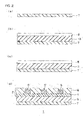
- FIG. 2 is a process diagram illustrating the steps of manufacturing the optical waveguide film shown in FIG. 1
- FIG. 3 is a process diagram illustrating the steps of manufacturing a film of the optical waveguide film shown in FIG. 1
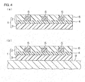
- FIG, 4 is a sectional view for explaining a method of fixing the optical waveguide film shown in FIG 1 to an optical substrate.
- the optical waveguide film 1 is formed in a band shape extending in the lengthwise direction, and includes a film 2 and an adhesive layer 3.
- the film 2 is an optical waveguide, which is formed so as to correspond to the outer shape of the optical waveguide film 1.
- the film 2 includes an under clad layer 4 serving as a clad layer and an over clad layer 6, and a core layer 5 covered by the under clad layer 4 and the over clad layer 6. More specifically, the film 2 includes an under clad layer 4, a core layer 5 formed on the under clad layer 4, and an over clad layer 6 formed on the under clad layer 4 so as to cover the core layer 5.
- a plurality (3) of the core layers 5 are provided on the upper surface of the under clad layer 4, extending in the lengthwise direction and arranged in parallel at spaced intervals to one another in the widthwise direction. Both lengthwise end portions of the core layer 5 serve as connecting portions to be optically connected with a plurality of optical elements.
- Each of the core layers 5 is formed in a generally rectangular shape in sectional view.
- the adhesive layer 3 is provided on one surface of the film 2, more specifically, on the lower surface of the under clad layer 4.
- the surface, that is, the lower surface of the adhesive layer 3 is formed in a rough structure, more specifically, in a rough structure having an arithmetic mean surface roughness or 0.1 to 2.0 ⁇ m.
- the lower surface of the adhesive layer 3 has an arithmetic mean surface roughness of preferably 0.1 to 0.5 ⁇ m, or more preferably 0.15 to 0.3 ⁇ m.
- the arithmetic mean surface roughness is determined as arithmetic mean Ra of the surface roughness obtained by the surface observation using a laser microscope.
- the arithmetic mean roughness is determined according to JIS B0601-1994.
- the adhesive layer has a storage modulus at 25°C of 10 to 100 MPa, preferably 10 to 70 MPa, or more preferably 10 to 30 MPa.
- the storage modulus at 25°C is determined as torsion storage modulus G' at 25°C obtained by dynamic viscoelastic measurement when the temperature is increased from -20°C to 200°C at a rate of 5°C/min in torsion mode with a frequency of 1 Hz.
- the opposite surface of the adhesive layer 3, more specifically, the upper surface (surface) to be in contact with the lower surface of the under clad layer 4) of the adhesive layer 3 is formed in a flat shape.
- the optical waveguide film 1 also includes a casting plate 7 (described later) which covers a surface (lower surface) of the adhesive layer 3 as required, as indicated by phantom lines in FIG. 1 .
- a casting plate 7 is first prepared, as shown in FIG. 2(a) .
- Examples of the material that may be used to form the casting plate 7 include ceramic materials such as silicon and glass; metallic materials such as copper, aluminium, stainless steel and iron alloy; and resin materials such as polyimide, glass-epoxy and polyethylene terephthalate (PET). From the viewpoint of ease of processing into a rough structure, a resin material is preferable, and PET is more preferable.
- ceramic materials such as silicon and glass
- metallic materials such as copper, aluminium, stainless steel and iron alloy
- resin materials such as polyimide, glass-epoxy and polyethylene terephthalate (PET). From the viewpoint of ease of processing into a rough structure, a resin material is preferable, and PET is more preferable.
- the surface of the casting plate 7, more specifically, the upper surface (surface to be in contact with an adhesive composition 13 which is subsequently coated) of the casting plate 7 is formed in a rough structure having an arithmetic mean surface roughness of 0. to 2.0 ⁇ m.
- the preferable range of the arithmetic mean surface roughness of the upper surface of the eating plate 7 is the same as that of the lower surface of the adhesive layer 3 as described above.
- the arithmetic mean surface roughness thereof is determined in the same manner as above.
- the rough structure on the surface of the casting plate 7 can be formed by a known method such as embossing.
- the casting plate 7 has a thickness of, for example, 10 to 5000 ⁇ m, or preferably 10 to 1500 ⁇ m.
- the adhesive composition 13 is coated onto the surface of the casting plate 7.
- the adhesive composition 13 does not substantially contain a solvent and forms the adhesive layer 3 by a curing method to be described later, and examples thereof include an acrylic adhesive composition.
- acrylic adhesive composition contains, for example, a monomer component or a partial polymer thereof, and an initiator.
- the acrylic monomer component mainly contains alkyl(meth)acrylate, and also contains the other components such as reactive functional group-containing vinyl monomer having a reactive functional group and copolymerizable vinyl monomer which is copolymerizable with the above monomers (alkyl (meth)acrylate and reactive functional group-containing vinyl monomer).
- the alkyl(meth)acrylate is alkyl methacrylate and/or alkyl acrylate, and examples thereof includes alkyl (meth)acrylates (having linear or branched alkyl moiety having 1 to 3 carbon atoms) such as methyl(meth)acrylate, ethyl (meth)acrylate, propyl (meth)acrylate and isopropyl (meth)acrylate; alkyl (meth)acrylate (having linear or branched alkyl moiety having 4 to 18 carbon atoms) such as butyl (meth)acrylate, isobutyl (meth)acrylate, see-butyl (meth)acrylate, t-butyl (meth)acrylate, pentyl (meth)acrylate neopentyl (meth)acrylate, isopentyl (meth)acrylate, hexyl (meth)acrylate, heptyl (meth)acrylate, octyl
- the amount of the alkyl(meth)acrylate is, for example, from 50 to 99.5 parts by weight per 100 parts by weight of the monomer component.
- Examples of the reactive functional group-containing vinyl monomer include carboxyl group-containing vinyl monomer, and examples of the carboxyl group -containing vinyl monomer include unsaturated carboxylic acids such as (meth)acrylic acid, fumaric acid, maleic acid, itaconic acid, crotonic acid and cinnamic acid; unsaturated dicarboxylic acid anhydrides such as fumaric anhydride, maleic anhydride and itaconic anhydride; unsaturated dicarboxylic acid monoesters such as monomethyl itaconate, monobutyl itaconate and 2-acryloyloxyethyl phthalate; unsaturated tricarboxylic acid monoesters such as 2-methacryloiloxyethyl trimellitate and 2-methacryloiloxyethyl pyromellitate; and carboxyalkyl acrylate such as carboxyethyl acrylate, and carboxypentyl acrylate.
- unsaturated carboxylic acids such as (me
- examples of the reactive functional group-containing vinyl monomer include epoxy group-containing vinyl monomers such as glycidyl (meth)acrylate and methyl glycidyl (meth)acrylate; hydroxyl group-containing vinyl monomers such as 2-hydroxyethyl acrylate, 2-hydroxypropyl acrylate, 2-hydroxybutyl acrylate, ethylene glycol (meth)acrylate and propylene glycol (meth)acrylate; amide group-containing vinyl monomers such as (meth)acrylamide, N,N-dimethyl (meth)acrylamide, N,N-diethyl (meth)acrylamide, N-isopropyl (meth)acrylamide, N-butyl (meth)acrylamide, N-methoxymethyl (meth)acrylamide, N-methylol (meth)acrylamide, N-methylolpropane (meth)acrylamide and N-vinylcarboxylic acid amide; amino group-containing vinyl monomers such as glycidyl (meth
- a carboxyl group-containing vinyl monomer is preferable.
- the amount of the reactive functional group-containing vinyl monomer is, for example, from 0.5 to 15 parts by weight per 100 parts by weight of the monomer component.
- Examples of the copolymerizable vinyl monomer include vinyl esters such as vinyl acetate and vinyl propionate; olefin-based monomers such as methylene, propylene, isoprene, butadiene and isobutylene; aryl (meth)acrylates such as phenyl (meth)acrylate; aromatic vinyl monomers such as styrene and vinyltoluene; nitrogen atom-containing vinyl monomers such as (meth)acryloyl morpholine, aminoethyl (meth)acrylate, N,N-dimethylaminoethyl (meth)acrylate, and t-butylaminoethyl (meth)acrylate; alkoxy group-containing vinyl monomers such as methoxyethyl (meth)acrylate, ethoxyethyl (meth)acrylate, (meth)acrylic acid methoxyethylene glycol and (meth)acrylic acid methoxypolypropylene glycol,
- Examples of the copolymerizable vinyl monomer include polyfunctional monomer.
- polyfunctional monomer examples include (mono or poly)alkylene polyol poly(meth)acrylates such as methylene glycol di(meth)acrylate, diethylene glycol di(meth)acrylate, triethylene glycol di(meth)acrylate, trimethylolpropane tri(meth)acrylate, tetraethylene glycol di(meth)acrylate, neopentyl glycol di(meth)acrylate, 1,6-hexandiol di(meth)acrylate, pentaerythritol di(meth)acrylate, tetramethylolmethane tri(meth)acrylate and dipentaerythritol hexa(meth)acrylate; and divinylbenzene.
- the polyfunctional monomer also include epoxy acrylate, polyester acrylate and urethane acrylate.
- a polyfunctional monomer is preferable.
- copolymerizable vinyl monomers can be used alone or in combination of two or more kinds.
- the amount of the copolymerizable vinyl monomer is, for example, 49 parts by weight or less, per 100 parts by weight of the monomer component.
- the partial polymer of the monomer component is a mixture of an unreacted monomer component and a polymer component, obtained by partially polymerizing (preliminarily polymerizing) a monomer component in the presence of an initiator.
- the polymerization rate of the partial polymer is, for example, from 2 to 40% by weight, or preferably from 5 to 20% by weight.
- the polymerization rate of the partial polymer can be calculated in the following process: About 0.5 g of a partial polymer is accurately weighed. After drying at 130°C for 2 hours, the partial polymer is again accurately weighed to obtain the amount of weight loss (volatile amount (unreacted monomer weight)). The numerical value thus obtained is substituted into the following equation
- the initiator examples include photopolymerization initiator and thermal polymerization initiator. From the viewpoint of ease of curing, a photopolymerization initiator is preferable.
- photopolymerization initiator examples include benzoin ethers such as benzoin methyl ether, benzoin isopropyl ether and 2,2-dimethoxy-1,2-diphenylethan-1-one; substituted benzoin ethers such as anisole methyl ether; substituted acetophenones such as 2,2-diethoxy acetophenone, 2,2-dimethoxy-2-phenylacetophenone and 1-hydroxy-cyclohexyl-phenyl ketone; substituted alpha-ketols such as 2-methyl-2-hydroxy propiophenone; aromatic sulfonyl chlorides such as 2-naphthalenesulfonyl chloride; and photoactive oximes such as 1-phenyl-1,1-propanedione-2-(o-ethoxycarbonyl)-oxime.
- benzoin ethers such as benzoin methyl ether, benzoin isopropyl ether and 2,2-dimethoxy-1,2-diphenylethan
- photopolymerization initiator examples thereof include IRGACURE series (manufactured by Ciba Specialty Chemicals Inc.), and specific examples thereof include IRGACURE 651 (2,2-dimethoxy-1,2-diphenylethan-1-one) and IRGACURE 184 (1-hydroxy-cyclohexyl-phenyl ketone).
- IRGACURE series manufactured by Ciba Specialty Chemicals Inc.
- specific examples thereof include IRGACURE 651 (2,2-dimethoxy-1,2-diphenylethan-1-one) and IRGACURE 184 (1-hydroxy-cyclohexyl-phenyl ketone).
- the amount of the initiator is, for example, from 0.01 to 5 parts by weight, or preferably from 0.1 to 3 parts by weight, per 100 parts by weight of the monomer component.
- the adhesive composition 13 can be obtained by formulating and mixing the monomer component and the initiator both described above.
- additives which are usually added to the adhesive composition, such as viscosity modifiers, and if necessary, crosslinking agents, release modifiers, plasticizers, softening agents, fillers, coloring agents (such as pigments and dyes) and antioxidants, can be added to the adhesive composition 13 at an appropriate ratio.
- viscosity modifier examples include styrene block polymer
- the adhesive composition 13 is coated by a coating method such as casting or spin coating.
- the thickness of the adhesive composition 13 thus coated is appropriately selected according to the thickness of the adhesive layer 3 that is subsequently formed, and is, for example, 10 ⁇ m or more, or preferably 20 ⁇ m or more and is usually 400 ⁇ m or less.
- the adhesive composition 13 is cured to form an adhesive layer 3.
- the adhesive composition 13 is cured, for examples, by light irradiation of the adhesive composition 13 when containing a photopolymerization initiator as an initiator, or by heating of the adhesive composition 13 when containing a thermal polymerization initiator as an initiator.
- the adhesive composition 13 is cured by light (ultraviolet light) irradiation.
- the ultraviolet light irradiation is performed, for example, at a dose of 400 to 4000 mJ/cm 2 with ultraviolet light having a wavelength of 300 to 400 nm whose irradiance is 1 to 200 mW/cm 2 .
- a release film 8 made of synthetic resin such as PET is laminated on the surface (upper surface) of the adhesive composition 13 thus coated to block oxygen from the adhesive composition 13.
- the surface (lower surface) of the release film 8 is subjected to release treatment such as silicone treatment as required in order to improve releasability from the adhesive layer 3.
- the adhesive composition 13 is cured to form an adhesive layer 3 having the above-mentioned storage modulus at 25°C of 10 to 100 MPa.
- the adhesive layer 3 thus formed has a thickness of, for example, 10 ⁇ m or more, or preferably 20 ⁇ m or more and is usually 400 ⁇ m or less.
- a film 2 including the under clad layer 4, the core layer 5 and the over clad layer 6 is prepared.
- a substrate 12 is prepared as shown in FIG. 3(a) .
- the substrate 12 has a plate shape, and examples of the material that may be used to form the substrate 12 include the same material as that used to form the casting plate 7 described above. From the viewpoint of ease of removal to be described later, a metallic material is preferable.
- the substrate 12 has a thickness of, for example, 10 to 5000 ⁇ m, or preferable 10 to 1500 ⁇ m.
- Examples of the material that may be used to form the under clad layer 4 include resin materials such as polyimide resin, polyamide resin, silicone resin, epoxy resin or fluorinated or deuterated resin obtained from any of these resins, and further fluorine derivative resin.
- resin materials such as polyimide resin, polyamide resin, silicone resin, epoxy resin or fluorinated or deuterated resin obtained from any of these resins, and further fluorine derivative resin.
- these resin materials are used in the form of photosensitive resins containing a photosensitizer.
- a photosensitive polyimide resin raw material: a photosensitive polyamic acid resin or a photosensitive fluorinated polyamic acid resin
- a photosensitive fluorene derivative resin raw material: a photosensitive fluorine
- a varnish (resin solution) of any of the above resins is prepared and then coated over the substrate 12 by a method such as casting or spin coating. Thereafter, the coated varnish is dried and then heated as required. In the case of using a photosensitive resin, after the coating and drying of the varnish, the coated varnish is exposed to light via a photomask and then heated as required. Thereafter, the heated varnish is developed and then heated.
- the under clad layer 4 thus formed has a thickness of, for example, 5 to 100 ⁇ m.
- a core layer 5 is formed on the under clad layer 4.
- Examples of the material that may be used to form the core layer 5 include resin materials having a higher refractive index than the resin material used for the under clad layer 4.
- Examples of the resin material include the same resin materials as those mentioned above.
- a varnish (resin solution) of any of the above resins is prepared, and the varnish is coated onto a surface of the under clad layer 4. Thereafter, the coated varnish is dried to be cured as required.
- the coated varnish is exposed to light via a photomask and then heated as required.
- Each of the core layers 5 thus formed has a thickness of, for example, 5 to 100 ⁇ m and a width of, for example, 5 to 100 ⁇ m.
- an over clad layer 6 is formed on the under clad layer 4 so as to cover the core layer 5.
- the material that may be used to form the over clad layer 6 includes the same resin material as that used for the under clad layer 4.
- the under clad layer 4 and the over clad layer 6 can be formed of the same resin material or of different resin materials.
- a varnish (resin solution) of any of the above resins is prepared and then coated over the under clad layer 4 including the core layer 5 by a method such as casting or spin coating. Whereafter, the coated varnish is dried and then heated as required. In the case of using a photosensitive resin, after the coating and drying of the varnish, the coated varnish is exposed to light via a photomask and then heated as required. Thereafter, the heated varnish is developed and then heated.
- the over clad layer 6 thus formed has a thickness of, for example, 5 to 100 ⁇ m.
- the substrate 12 is removed.
- etching or peeling is used to remove the substrate 12.
- the film 2 including the under clad layer 4, the core layer 5 and the over clad layer 6 can be prepared.
- the under clad layer 4 is adhesively bonded to a flat surface (a surface opposite to the surface in contact with the casting plate 7) of the adhesive layer 3.
- the lower surface of the under clad layer 4 in the film 2 is bonded to the upper surface of the adhesive layer 3 (the flat surface of the adhesive layer 3).
- the optical waveguide film 1 can be obtained.
- the initial adhesive strength of the adhesive layer 3 to be described in detail in the following EXAMPLES is, for example, 0.5 N/cm or less, or preferably 0.2 N/cm or less and usually 0.1 N/cm or more while the adhesive strength after press-bonding of the adhesive layer 3 is, for example, 1 N/cm or more, or preferably 1.1 N/cm or more and usually 3 N/cm or less.
- the casting plate 7 (cf. FIG. 2(d) ) is removed from the adhesive layer 3 in the optical waveguide film 1 thus obtained. This exposes the lower surface of the adhesive layer 3 having a rough structured.
- the optical waveguide film 1 is fixed to the optical substrate 9 provided with an optical element (not shown).
- the lower surface of the adhesive layer 3 is once brought into contact (initial adhesion) with the upper surface of the optical substrate 9, while the optical waveguide film 1 is positioned to the optical substrate 9 from above so as to adjoin the optical element.
- the optical waveguide film 1 is positioned to the optical substrate 9 so that the connecting portion of the core layer 5 is optically connected with the connecting portion of the optical element, the optical waveguide film 1 is fixed onto the optical substrate 9 by directly press-bonding the optical waveguide film 1 downward.
- the optical waveguide film 1 is pulled upward to remove the adhesive layer 3 from the optical substrate 9. Then, the optical waveguide film 1 is positioned (corrected its position) to the optical substrate 9, and the lower surface of the adhesive layer 3 is brought into contact with the upper surface of the optical substrate 9. Thereafter, when the optical waveguide film 1 is positioned to the optical substrate 9 so that the connecting portion off the core layer 5 is optically connected with the connecting portion of the optical element, the optical waveguide film 1 is fixed onto the optical substrate 9. When the optical waveguide film 1 is not positioned to the optical substrate 9, the peeling and the adhesion as described above are repeated.
- the rough structure having the specific surface roughness on the upper surface of the casting plate 7 is transferred onto the lower surface of the adhesive layer 3 formed of the adhesive composition 13 that has been coated on the upper surface of the casting plate 7. This transfer allows accurate and easy formation of the adhesive layer 3 having a rough-structured lower surface with a specific surface roughness.
- the method of manufacturing the optical waveguide film 1 can secure sufficient contact area between the under clad layer 4 and the adhesive layer 3, thereby reliably adhering the under clad layer 4 to the adhesive layer 3.
- the initial adhesive strength can be reduced because the optical substrate 9 is brought into contact with the rough-structured lower surface of the adhesive layer 3 having a specific surface roughness. This facilitates peeling during positioning, thereby obtaining excellent positioning accuracy.
- the adhesive layer 3 has a specific storage modulus, when it is adhered (press-bonded) to the optical substrate 9 after the initial adhesion, sufficient adhesive strength can be secured by press-bonding the rough-structured lower surface of the adhesive layer 3 having a specific surface roughness to the optical substrate 9, so that the film 2 can be securely fixed onto the optical substrate 9.
- the adhesive layer 3 since the adhesive layer 3 has a specific storage modulus, the flowage of the adhesive layer 3 is suppressed in the initial adhesion to the optical substrate 9, thereby preventing the adhesive layer 3 from blocking the optical path between the connecting portion of the core laser 5 and the connecting portion of the optical element.
- the adhesive layer 3 was provided only on the lower surface of the under clad layer 4. However, the adhesive layer 3 can also be provided on the upper surface of the over clad layer 6.
- Example 1 The present invention will now be described in more detail by way of Examples and Comparative Examples. However, the present invention is not limited to the following Examples and Comparative Examples. In the following description, the units “part(s)” and “%” are by weight, unless otherwise noted, Example 1
- a PET film (EMBLET SM-38, thickness: 38 ⁇ m, size: 200 x 300 mm, manufactured by Unitika, Ltd.) subjected to processing (sand mat treatment) to form a rough structure on its upper surface was prepared (cf. FIG. 2(a) ).
- an adhesive composition was coated onto the upper surface of the PET film so as to have a thickness after curing of 40 ⁇ m (cf. FIG. 2(b) ). Thereafter, the adhesive composition was adhesively bonded to a 35 ⁇ m-thick PET release film of which the lower surface was subjected to silicone treatment (release treatment) so that the adhesive composition was in contact with the lower surface of the release file, thereby blocking oxygen from the adhesive composition (cf. FIG. 2(b) (phantom lines)).
- ultraviolet light (wavelength: 315 to 400 nm) was irradiated thereto from the upper side of the release film with a black light (manufactured by Toshiba Corp.) at a irradiance of 3.6 mW/cm 2 for 5 minutes to cure the adhesive composition, thereby forming an adhesive layer sandwiched between the PET film and the release film (cf. FIG. 2(c) ).
- a substrate (200 x 300 in size) made of a 25 ⁇ m-thick stainless steel was prepared (cf FIG. 3(a) ).
- a fluorene derivative varnish A was prepared according to the formulation shown in Table 1.
- the fluorene derivative varnish A thus prepared was coated onto a surface of the stainless steel substrate, and the coated varnish was heated at 100°C for 15 minutes to dry. Thereafter, the dried varnish was exposed to light via a photomask and then developed.
- the developed varnish was heated at 100°C for 20 minutes to be cured, thereby forming an under clad layer on the stainless steel substrate (cf. FIG. 3(b) ),
- the under clad layer had a refractive index of 1.585 at a wavelength of 633 nm.
- the under clad layer had a thickness: of 20 ⁇ m.
- a fluorene derivative varnish B was prepared according to the formulation shown in Table 1.
- the fluorene derivative varnish B thus prepared was coated onto a surface of the under clad layer, and the coated varnish was heated at 100°C for 30 minutes to dry. Whereafter, the dried varnish was exposed to light via a photomask, After the exposure, the varnish was heated at 100°C for 60 minutes and then developed. Subsequently, the developed varnish was heated at 100°C for 10 minutes to be cured, thereby forming a core layer on the under clad laser.
- the core layer had a refractive index of 1.615 at a wavelength of 633 nm.
- the core layer had a thickness of 5 ⁇ m and a width of 5 ⁇ m.
- the fluorine derivative varnish A was then coated onto a surface of the under clad layer containing the core layer, and the coated varnish was heated at 100°C for 15 minutes to dry. Thereafter, the dried varnish was exposed to light via a photomask and then developed, The developed varnish was heated at 100°C for 20 minutes to be cured, thereby forming an over clad layer on the under clad layer so as to cover the core layer (cf. FIG. 3(d) ).
- the over clad layer had a refractive index of 1.585 at a wavelength of 633 nm.
- the over clad layer had a thickness of 20 ⁇ m
- the release film was removed from the adhesive layer, and the lower surface of the under clad layer in the film was bonded to the upper surface of the adhesive layer (cf. FIG. 2(d) ).
- an optical waveguide film including the film and the adhesive layer was produced.
- Example 2 In the same manner as in Example 1, except that the adhesive composition was coated so as to have a thickness after curing of 70 ⁇ m in the formation of the adhesive layer in Example 1, an adhesive layer was formed, and subsequently, an optical waveguide film was produced.
- Example 2 In the same manner as in Example 1, except that the adhesive composition was coated so as to have a thickness after curing of 120 ⁇ m in the formation of the adhesive layer in Example 1, an adhesive layer was formed, and subsequently, an optical waveguide film was produced.
- Example 4 In the same manner as in Example 5, except that 15 parts of acrylic acid was used in place of 10 parts of acrylic acid in the preparation of the adhesive composition in Example 4, an adhesive composition containing a partial polymer was prepared, an adhesive layer (thickness: 40 ⁇ m) was then formed, and subsequently, an optical waveguide film was produced.
- the polymerization rate of the partial polymer was 8%.
- Example 2 In the same manner as in Example 1, except that a normal PET firm (PET film not processed into a rough structure) was used in place of the PET film processed into a rough structure in the formation of the adhesive layer in Example 1, an adhesive layer was formed, and subsequently, an optical waveguide film was produced.
- a normal PET firm PET film not processed into a rough structure
- Example 4 In the same manner as in Example 4, except that a normal PET film (PET film not processed into a rough structure) was used in place of the PET film processed into a rough structure in the formation of the adhesive layer in Example 4, an adhesive layer was formed, and subsequently, an optical waveguide film was produces.
- PET film not processed into a rough structure PET film not processed into a rough structure
- Example 5 In the same manner as in Example 5, except that a normal PET film (PET film not processed into a rough structure) was used in place of the PET film processed into a rough structure in the formation of the adhesive layer in Example 5, an adhesive layer was formed, and subsequently an optical waveguide film was produced.
- PET film not processed into a rough structure PET film not processed into a rough structure
- a PET film (EMBLET SM-38, thickness: 38 ⁇ m, manufactured by Unitika, Ltd.) having the upper surface subjected to processing (sand mat treatment) into a rough structure was prepared (cf. FIG. 2(a) ). Subsequently, an adhesive solution was coated onto the upper surface of the PET film so as to have a thickness after drying of 40 ⁇ m (cf. FIG. 2(b) ).
- the PET film thus coated with the adhesive was then put into a dryer at 130°C for 3 minutes to volatilize the residual monomers, thereby forming an adhesive layer (see FIG. 2(c) ).
- the lower surface of the under clad layer in the film was bonded to the upper surface of the adhesive layer (cf. FIG, 3(d) ).
- a dynamic viscoelasticity measuring device (ARES, manufactured by TA instruments Co., Ltd.) was used to calculate a storage modulus at 25°C by increasing the temperature from -20°C to 200°C at 5°C/min in torsion mode with a frequency of 1 Hz. The results are shown in Table 2.
- the upper surface of the PET film processed into a rough structure and the lower surface of the adhesive layer formed according to each of Examples and Comparative Examples were subjected to surface observation using a laser microscope (1LM21H, manufactured by Lasertec Corporation) to determine the arithmetic mean surface roughness Ra.
- the arithmetic mean surface roughness Ra was calculated according to JIS B0601-1994.
- the upper surface of the PET film processed into a rough structure had an arithmetic mean surface roughness Ra of 0.18 ⁇ m.
- Table 2 shows the arithmetic mean surface roughness Ra of the lower surface of the adhesive layer formed according to each of Examples and Comparative Examples.
- FIGS. 5 and 6 Image-processed pictures of the lower surface of the adhesive layer in Example 1 by surface observation using a laser microscope are shown in FIGS. 5 and 6.
- FIG. 5 is a rear view showing the lower surface of the adhesive layer
- FIG. 6 is a perspective view showing the lower surface of the adhesive layer.
- the adhesive layer of the optical waveguide film thus obtained was bonded to the optical substrate made of silicon using a roll with a pressure of 400 kPa at a temperature of 130°C. After the optical waveguide film thus bonded was allowed to stand at 23°C for 30 minutes, one end of the optical waveguide film was peeled off in a direction 90° relative to the optical substrate at a rate of 50 mm/min to measure the resistance (90° peel test). In the 90° peel test, the resistance was not measured until the optical waveguide film was peeled off to 10 mm from the end thereof. When exceeding 10 mm, the measurement was started to determine the minimum resistance as an adhesive strength after press-bonding. The results are shown in Table 2. Table 2 [TABLE 2] Ex./Comp. Ex. Ex.
Landscapes
- Physics & Mathematics (AREA)
- Engineering & Computer Science (AREA)
- Microelectronics & Electronic Packaging (AREA)
- General Physics & Mathematics (AREA)
- Optics & Photonics (AREA)
- Optical Integrated Circuits (AREA)
Applications Claiming Priority (1)
| Application Number | Priority Date | Filing Date | Title |
|---|---|---|---|
| JP2007199994A JP2009036923A (ja) | 2007-07-31 | 2007-07-31 | 光導波路フィルムおよびその製造方法 |
Publications (1)
| Publication Number | Publication Date |
|---|---|
| EP2034341A2 true EP2034341A2 (de) | 2009-03-11 |
Family
ID=40279716
Family Applications (1)
| Application Number | Title | Priority Date | Filing Date |
|---|---|---|---|
| EP08161404A Withdrawn EP2034341A2 (de) | 2007-07-31 | 2008-07-30 | Optische Wellenleiterfolie und Herstellungsverfahren dafür |
Country Status (5)
| Country | Link |
|---|---|
| US (1) | US7856165B2 (de) |
| EP (1) | EP2034341A2 (de) |
| JP (1) | JP2009036923A (de) |
| KR (1) | KR20090013118A (de) |
| CN (1) | CN101359069B (de) |
Families Citing this family (6)
| Publication number | Priority date | Publication date | Assignee | Title |
|---|---|---|---|---|
| EP2366270A4 (de) * | 2008-12-02 | 2013-04-10 | Univ Arizona | Verfahren zur herstellung einer flexiblen substratabnordnung und flexible substratabnordnung daraus |
| CN101933081B (zh) | 2009-02-19 | 2013-10-23 | 松下电器产业株式会社 | 图像显示装置和图像显示方法 |
| JP2011039489A (ja) * | 2009-07-17 | 2011-02-24 | Nitto Denko Corp | 光導波路装置の製造方法 |
| JP2015114390A (ja) * | 2013-12-09 | 2015-06-22 | 住友ベークライト株式会社 | 接着シート、接着シート付き光導波路、光電気混載基板、光電気混載基板の製造方法、光モジュールおよび電子機器 |
| JP6624065B2 (ja) | 2014-11-18 | 2019-12-25 | 日立化成株式会社 | 半導体装置及びその製造方法、並びに可撓性樹脂層形成用樹脂組成物 |
| JP6855210B2 (ja) * | 2015-11-24 | 2021-04-07 | 日東電工株式会社 | 粘着シート貼付け方法および粘着シート貼付け装置 |
Family Cites Families (7)
| Publication number | Priority date | Publication date | Assignee | Title |
|---|---|---|---|---|
| JP3185797B2 (ja) * | 1999-12-08 | 2001-07-11 | 日立電線株式会社 | 接着シート付き導波路フィルム及びその実装方法 |
| JP4453184B2 (ja) | 2000-10-10 | 2010-04-21 | 凸版印刷株式会社 | 光基板の製造方法 |
| JP3733418B2 (ja) * | 2001-04-16 | 2006-01-11 | シャープ株式会社 | 粘接着シート、積層シート及び液晶表示装置 |
| US20070172649A1 (en) * | 2004-03-19 | 2007-07-26 | Mitsui Chemicals, Inc. | Adhesive material, pressure sensitive adhesive film and method of use thereof |
| JP4825404B2 (ja) * | 2004-04-12 | 2011-11-30 | 王子タック株式会社 | 粘着シートおよびその製造方法 |
| JP2006030294A (ja) * | 2004-07-12 | 2006-02-02 | Nitto Denko Corp | フレキシブル光導波路の製法 |
| JP2007017521A (ja) * | 2005-07-05 | 2007-01-25 | Lintec Corp | 平面型光導波路作製用樹脂シート |
-
2007
- 2007-07-31 JP JP2007199994A patent/JP2009036923A/ja active Pending
-
2008
- 2008-07-30 CN CN2008101442831A patent/CN101359069B/zh not_active Expired - Fee Related
- 2008-07-30 KR KR1020080074728A patent/KR20090013118A/ko not_active Withdrawn
- 2008-07-30 EP EP08161404A patent/EP2034341A2/de not_active Withdrawn
- 2008-07-31 US US12/222,036 patent/US7856165B2/en not_active Expired - Fee Related
Also Published As
| Publication number | Publication date |
|---|---|
| CN101359069B (zh) | 2012-06-27 |
| KR20090013118A (ko) | 2009-02-04 |
| JP2009036923A (ja) | 2009-02-19 |
| CN101359069A (zh) | 2009-02-04 |
| US7856165B2 (en) | 2010-12-21 |
| US20090067798A1 (en) | 2009-03-12 |
Similar Documents
| Publication | Publication Date | Title |
|---|---|---|
| KR101114361B1 (ko) | 점착제 | |
| EP2034341A2 (de) | Optische Wellenleiterfolie und Herstellungsverfahren dafür | |
| TWI404783B (zh) | 壓感性黏合組成物以及含彼之偏光板與液晶顯示器 | |
| TW201219481A (en) | Optical resin composition, optical resin material using the same, optical filter for image display device, and image display device | |
| CN111164176B (zh) | 粘着剂组合物及粘着片 | |
| CN101033380A (zh) | 压敏粘合剂及其片材、起偏振片和光学薄膜及其生产方法 | |
| JP4969744B2 (ja) | 粘着組成物及び粘着シート | |
| TW201704423A (zh) | 黏著劑層及黏著膜 | |
| KR20140133875A (ko) | 표면보호시트, 전자기기 및 전자기기 부품의 제조방법 | |
| CN118369392A (zh) | 粘合剂组合物和粘合片 | |
| JP7380578B2 (ja) | 表面保護シート用粘着剤組成物及び表面保護シート | |
| TWI698333B (zh) | 積層體之製造方法 | |
| TWI824013B (zh) | 表面保護薄片用黏著劑組成物及表面保護薄片 | |
| JP7079808B2 (ja) | 粘着剤層の製造方法、及び粘着フィルムの製造方法 | |
| KR20150093447A (ko) | 점착제 조성물 | |
| JP2014094977A (ja) | 画像表示装置用粘着シート、画像表示装置の製造方法及び画像表示装置 | |
| CN114517069A (zh) | 一种粘着剂组合物、一种uv减粘胶带及其制备方法 | |
| KR20110082333A (ko) | 편광판 및 이를 포함하는 액정표시장치 | |
| EP2023173A1 (de) | Optische Wellenleiterfolie und Herstellungsverfahren dafür | |
| JPH06264033A (ja) | 光硬化型接着剤組成物 | |
| KR20120109412A (ko) | 광학 필름용 점착제 조성물 | |
| TW202111052A (zh) | 黏著片材、及黏著片材貼附品之製造方法 | |
| CN114026192A (zh) | 粘合片、及粘合片贴附品的制造方法 | |
| KR20090003831A (ko) | 편광판용 점착제 조성물, 이를 이용한 편광판 및액정표시장치 | |
| KR20230075430A (ko) | 세퍼레이터 부가 광학 점착 시트 |
Legal Events
| Date | Code | Title | Description |
|---|---|---|---|
| PUAI | Public reference made under article 153(3) epc to a published international application that has entered the european phase |
Free format text: ORIGINAL CODE: 0009012 |
|
| AK | Designated contracting states |
Kind code of ref document: A2 Designated state(s): AT BE BG CH CY CZ DE DK EE ES FI FR GB GR HR HU IE IS IT LI LT LU LV MC MT NL NO PL PT RO SE SI SK TR |
|
| AX | Request for extension of the european patent |
Extension state: AL BA MK RS |
|
| STAA | Information on the status of an ep patent application or granted ep patent |
Free format text: STATUS: THE APPLICATION HAS BEEN WITHDRAWN |
|
| 18W | Application withdrawn |
Effective date: 20090519 |