EP2027647B1 - Dispositif d'alimentation électrique dans un réseau d'alimentation électrique et convertisseur de tension continue destiné à un tel dispositif - Google Patents
Dispositif d'alimentation électrique dans un réseau d'alimentation électrique et convertisseur de tension continue destiné à un tel dispositif Download PDFInfo
- Publication number
- EP2027647B1 EP2027647B1 EP08757930A EP08757930A EP2027647B1 EP 2027647 B1 EP2027647 B1 EP 2027647B1 EP 08757930 A EP08757930 A EP 08757930A EP 08757930 A EP08757930 A EP 08757930A EP 2027647 B1 EP2027647 B1 EP 2027647B1
- Authority
- EP
- European Patent Office
- Prior art keywords
- winding
- inverter
- windings
- direct voltage
- switch
- Prior art date
- Legal status (The legal status is an assumption and is not a legal conclusion. Google has not performed a legal analysis and makes no representation as to the accuracy of the status listed.)
- Not-in-force
Links
Images


Classifications
-
- H—ELECTRICITY
- H02—GENERATION; CONVERSION OR DISTRIBUTION OF ELECTRIC POWER
- H02M—APPARATUS FOR CONVERSION BETWEEN AC AND AC, BETWEEN AC AND DC, OR BETWEEN DC AND DC, AND FOR USE WITH MAINS OR SIMILAR POWER SUPPLY SYSTEMS; CONVERSION OF DC OR AC INPUT POWER INTO SURGE OUTPUT POWER; CONTROL OR REGULATION THEREOF
- H02M3/00—Conversion of dc power input into dc power output
- H02M3/02—Conversion of dc power input into dc power output without intermediate conversion into ac
- H02M3/04—Conversion of dc power input into dc power output without intermediate conversion into ac by static converters
- H02M3/10—Conversion of dc power input into dc power output without intermediate conversion into ac by static converters using discharge tubes with control electrode or semiconductor devices with control electrode
- H02M3/145—Conversion of dc power input into dc power output without intermediate conversion into ac by static converters using discharge tubes with control electrode or semiconductor devices with control electrode using devices of a triode or transistor type requiring continuous application of a control signal
- H02M3/155—Conversion of dc power input into dc power output without intermediate conversion into ac by static converters using discharge tubes with control electrode or semiconductor devices with control electrode using devices of a triode or transistor type requiring continuous application of a control signal using semiconductor devices only
-
- H—ELECTRICITY
- H02—GENERATION; CONVERSION OR DISTRIBUTION OF ELECTRIC POWER
- H02M—APPARATUS FOR CONVERSION BETWEEN AC AND AC, BETWEEN AC AND DC, OR BETWEEN DC AND DC, AND FOR USE WITH MAINS OR SIMILAR POWER SUPPLY SYSTEMS; CONVERSION OF DC OR AC INPUT POWER INTO SURGE OUTPUT POWER; CONTROL OR REGULATION THEREOF
- H02M7/00—Conversion of ac power input into dc power output; Conversion of dc power input into ac power output
- H02M7/42—Conversion of dc power input into ac power output without possibility of reversal
- H02M7/44—Conversion of dc power input into ac power output without possibility of reversal by static converters
- H02M7/48—Conversion of dc power input into ac power output without possibility of reversal by static converters using discharge tubes with control electrode or semiconductor devices with control electrode
-
- H—ELECTRICITY
- H02—GENERATION; CONVERSION OR DISTRIBUTION OF ELECTRIC POWER
- H02J—CIRCUIT ARRANGEMENTS OR SYSTEMS FOR SUPPLYING OR DISTRIBUTING ELECTRIC POWER; SYSTEMS FOR STORING ELECTRIC ENERGY
- H02J3/00—Circuit arrangements for ac mains or ac distribution networks
- H02J3/38—Arrangements for parallely feeding a single network by two or more generators, converters or transformers
- H02J3/381—Dispersed generators
-
- H—ELECTRICITY
- H02—GENERATION; CONVERSION OR DISTRIBUTION OF ELECTRIC POWER
- H02M—APPARATUS FOR CONVERSION BETWEEN AC AND AC, BETWEEN AC AND DC, OR BETWEEN DC AND DC, AND FOR USE WITH MAINS OR SIMILAR POWER SUPPLY SYSTEMS; CONVERSION OF DC OR AC INPUT POWER INTO SURGE OUTPUT POWER; CONTROL OR REGULATION THEREOF
- H02M7/00—Conversion of ac power input into dc power output; Conversion of dc power input into ac power output
- H02M7/02—Conversion of ac power input into dc power output without possibility of reversal
- H02M7/04—Conversion of ac power input into dc power output without possibility of reversal by static converters
- H02M7/12—Conversion of ac power input into dc power output without possibility of reversal by static converters using discharge tubes with control electrode or semiconductor devices with control electrode
- H02M7/145—Conversion of ac power input into dc power output without possibility of reversal by static converters using discharge tubes with control electrode or semiconductor devices with control electrode using devices of a thyratron or thyristor type requiring extinguishing means
- H02M7/155—Conversion of ac power input into dc power output without possibility of reversal by static converters using discharge tubes with control electrode or semiconductor devices with control electrode using devices of a thyratron or thyristor type requiring extinguishing means using semiconductor devices only
-
- H—ELECTRICITY
- H02—GENERATION; CONVERSION OR DISTRIBUTION OF ELECTRIC POWER
- H02J—CIRCUIT ARRANGEMENTS OR SYSTEMS FOR SUPPLYING OR DISTRIBUTING ELECTRIC POWER; SYSTEMS FOR STORING ELECTRIC ENERGY
- H02J2300/00—Systems for supplying or distributing electric power characterised by decentralized, dispersed, or local generation
- H02J2300/20—The dispersed energy generation being of renewable origin
- H02J2300/22—The renewable source being solar energy
- H02J2300/24—The renewable source being solar energy of photovoltaic origin
-
- H—ELECTRICITY
- H02—GENERATION; CONVERSION OR DISTRIBUTION OF ELECTRIC POWER
- H02M—APPARATUS FOR CONVERSION BETWEEN AC AND AC, BETWEEN AC AND DC, OR BETWEEN DC AND DC, AND FOR USE WITH MAINS OR SIMILAR POWER SUPPLY SYSTEMS; CONVERSION OF DC OR AC INPUT POWER INTO SURGE OUTPUT POWER; CONTROL OR REGULATION THEREOF
- H02M1/00—Details of apparatus for conversion
- H02M1/0067—Converter structures employing plural converter units, other than for parallel operation of the units on a single load
- H02M1/007—Plural converter units in cascade
-
- H—ELECTRICITY
- H02—GENERATION; CONVERSION OR DISTRIBUTION OF ELECTRIC POWER
- H02M—APPARATUS FOR CONVERSION BETWEEN AC AND AC, BETWEEN AC AND DC, OR BETWEEN DC AND DC, AND FOR USE WITH MAINS OR SIMILAR POWER SUPPLY SYSTEMS; CONVERSION OF DC OR AC INPUT POWER INTO SURGE OUTPUT POWER; CONTROL OR REGULATION THEREOF
- H02M7/00—Conversion of ac power input into dc power output; Conversion of dc power input into ac power output
- H02M7/42—Conversion of dc power input into ac power output without possibility of reversal
- H02M7/44—Conversion of dc power input into ac power output without possibility of reversal by static converters
- H02M7/48—Conversion of dc power input into ac power output without possibility of reversal by static converters using discharge tubes with control electrode or semiconductor devices with control electrode
- H02M7/483—Converters with outputs that each can have more than two voltages levels
- H02M7/487—Neutral point clamped inverters
-
- Y—GENERAL TAGGING OF NEW TECHNOLOGICAL DEVELOPMENTS; GENERAL TAGGING OF CROSS-SECTIONAL TECHNOLOGIES SPANNING OVER SEVERAL SECTIONS OF THE IPC; TECHNICAL SUBJECTS COVERED BY FORMER USPC CROSS-REFERENCE ART COLLECTIONS [XRACs] AND DIGESTS
- Y02—TECHNOLOGIES OR APPLICATIONS FOR MITIGATION OR ADAPTATION AGAINST CLIMATE CHANGE
- Y02E—REDUCTION OF GREENHOUSE GAS [GHG] EMISSIONS, RELATED TO ENERGY GENERATION, TRANSMISSION OR DISTRIBUTION
- Y02E10/00—Energy generation through renewable energy sources
- Y02E10/50—Photovoltaic [PV] energy
- Y02E10/56—Power conversion systems, e.g. maximum power point trackers
Definitions
- the invention relates to a device of the type specified in the preamble of claim 1 and a suitable DC-DC converter.
- DC generators For feeding electrical energy with DC generators such.
- B. photovoltaic or fuel cell systems is generated, in an AC network, in particular the public power grid (50/60 Hz), inverters of various kinds are used.
- a DC-DC converter is provided in most cases, which serves the purpose of converting the DC voltage supplied by the DC voltage generator into a required by the inverter or adapted to this DC voltage.
- a grounding of the type described is readily possible when DC-DC converters are used with transformers, which cause a galvanic separation of the DC side from the AC side.
- transformers regardless of whether mains transformers or high-frequency transformers are used, u. a. a reduction of the efficiency, sometimes considerable weights and sizes and / or an additional control effort result, which is why transformerless voltage transformers are preferred.
- transformerless DC-DC converters either make the desired grounding impossible, as this would result in the short circuiting of required switches, capacitors, or the like, or result in increased circuit complexity and other disadvantages.
- circuits which serve the purpose of reducing the unwanted leakage currents (eg. DE 10 2004 037 446 A1 . DE 102 21 592 A1 . DE 10 2004 030 912 B3 ).
- DE 10 2004 037 446 A1 . DE 102 21 592 A1 . DE 10 2004 030 912 B3 operated a solar generator in certain phases of the internal electric energy transport isolated from the grid.
- parasitic capacitances are only slightly reloaded, so that the potential of the solar generator with grid frequency sinusoidal and at a voltage amplitude of half the mains voltage corresponds, changes.
- High-frequency currents are then formed by the low voltage differences of the solar generator only between two switching cycles and by asymmetries during switching off. Capacitive leakage currents can therefore be greatly minimized in this way, but in principle not completely avoided.
- circuit arrangements are already known with which a solar generator can be grounded on one side despite the absence of a transformer. As a result, capacitive leakage currents are inherently prevented.
- One of these circuit arrangements ( DE 196 42 522 C1 ), however, requires five active switches, with one or two switches simultaneously switching to high-frequency and providing the average output current. In this circuit, also referred to as "flying inductor", the efficiency is therefore impaired by the high number of components involved in the current flow simultaneously in series.
- a disadvantage of this circuit also that lückende current pulses are impressed into the network, which make a capacitive line filter required that degrades the inherent by its own reactive power demand the power factor, but also the efficiency of the circuit in the partial load range.
- devices of the type described are known ( US 2007/0047277 A1 ), which are intended for inverters with a bipolar voltage intermediate circuit, which contains two series-connected capacitors connected to one earth connection.
- Such inverters which are used today predominantly for the purposes of interest here, can be designed as so-called half-bridge inverters, as half-bridge inverters in a 3-point circuit and as required as an inverter for a single-phase or three-phase grid feed.
- the connection point between the two capacitors forms a ground connection which is assigned to the neutral or neutral conductor of the respective network and is connected to it.
- the DC-DC converter of this known device includes a storage inductor, two diodes and a switch.
- the ground connection of the inverter can in this case be connected to the negative output of the DC voltage generator.
- a storage choke which is composed of two magnetically coupled windings.
- the two windings of this storage inductor are so galvanically connected at one end, that on the one hand with the switch closed one of the two windings of the DC voltage generator and the other winding is charged due to the magnetic coupling on the first winding and that on the other hand with an open switch both windings are discharged via an associated one of the two capacitors and an associated diode.
- the technical problem of the invention is the device of the type described and in particular a suitable DC-DC converter so that a grounding of the negative terminal of the DC generator not only with comparatively simple design means, but can be realized with significant reduction of the voltage load of the switch of the DC-DC converter.
- the invention enables a grounded operation of the DC voltage generator by using a DC-DC converter, which requires in the simplest case, only one storage inductor, three diodes and two switches.
- a DC-DC converter which requires in the simplest case, only one storage inductor, three diodes and two switches.
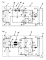
- Fig. 1 contains a conventional, considered within the scope of the present invention device a DC voltage generator 1, a DC-DC converter 2 and an inverter 3.
- the DC voltage generator 1 is z. B. from a photovoltaic or fuel cell system and has its two outputs 4 (+) and 5 (-) connected in parallel capacitor C (eg. US 2007 / 0047277A1 , Fig. 10).
- the inverter 3 of the known device has two outputs 6 and 7, which serve here for single-phase supply of electrical energy into a power supply network 8, whose phase L is connected to the output 6 and the neutral or neutral conductor N to the output 7.
- the inverter 3 also includes three inputs E1, E2 and E3. Between the inputs E1 and E2 two series-connected capacitors C1 and C2 are arranged, whose connection point is located at the input E3.
- the capacitors C1 and C2 form a conventional, bipolar voltage intermediate circuit of the inverter 3.
- the inverter 3 is according to Fig. 1 designed as a half-bridge inverter and provided with two switches S1 and S2, whose one.
- Connection is connected to one of the inputs E1 and E2 and their other connection to a common connection point 9 and from there via a smoothing or line reactor L1 to the output 6 leads.
- Both switches S1, S2 are also each a diode D1, D2 connected in parallel, the diode D1 from the connection point 9 in the direction of the input E1 and the diode D2 from the input E3 in the direction of the connection point 9 can be made conductive and in the opposite Direction locks.
- the input E3 is connected directly to the output 7, on the other hand connected to ground and thus formed as a ground terminal and connected to the negative output 5 of the DC voltage generator 1.
- the DC-DC converter 2 has two to be connected to the outputs 4 and 5 of the DC voltage generator 1 inputs 10 and 11.
- a switch S4 is connected to a connection point 14 leads.
- connection point 14 of the one terminal of a throttle designed as a coupled storage throttle 15 is connected.
- the storage inductor 15 includes a first winding W1 and a second winding W2, both magnetically coupled together and z. B. are wound on a common core 16. At one end, the two windings W1, W2 are connected together to form a further connection point.
- the input E3 of the inverter 3 designed as a ground connection is galvanically connected not only to the input 11 to be connected to the negative output 5 of the DC voltage generator 1, but also to the connection point of the two windings W1, W2 of the DC voltage converter 2.
- the other terminal of the winding W2 is connected via a diode D4 to the input E1 and the input E2 via a further diode D5 to the connection point 14 between the switch S4 and the winding W1.
- a first circuit, starting from the input 10 of the DC-DC converter 3, is formed by the switch S4, the winding W1 connected in series therewith and a power leading from the connection point of the two windings W1, W2 to the input 11.
- a second circuit contains the first winding W1 and leads back from the connection point 14 via the first winding W1, the ground terminal E3, a capacitor C2 associated with the winding W1, and the diode D5, all in series, to the connection point 14.
- a third circuit Finally, the second winding W2 and leads from the connection point of the two windings W1, W2 via the winding W2 and the diode D4 to the input E1, from there via the other of the two, the winding W2 associated capacitor C1 to the ground terminal E3 and from there back to the connection point between the two windings W1 and W2.
- the two windings W1, W2 are wound on the common core 16 such that the winding W2 is also charged when the winding W1 is charged due to the magnetic coupling through the first winding W1.
- the winding sense of both windings W1, W2 is chosen so that at in Fig. 1 indicated by points indicated points the same voltage polarities are obtained.
- the switches S1, S2 and S4 are expediently designed in a known manner as a semiconductor switch, which can be periodically switched on and off during operation with control units, not shown (microcontroller, PWM controllers, etc.), wherein the switching frequency z. B. 16 kHz or more.
- the switches S1, S2 are alternately turned on and off. This z. B. during the positive half cycle of the switching signal (switch S1 initially closed, switch S2 open) the positive side relative to E3 (input E1) of the capacitor C1 via the connection point 9 and the line choke L1 to the phase L. At the subsequent opening of the switch S1, the current can flow through the line reactor L1, the capacitor C2 and the diode D2.
- the negative side (input E2) of the capacitor C2 is connected to the phase L via the connection point 9 and the inductor L1 Close the switch S2 can continue to flow through the diode D1 and the capacitor C1.
- the two capacitors C1, C2 are thereby alternately discharged and recharged.
- the described design of the DC-DC converter 2 has the advantage that the DC voltage generator 1 can be operated with a comparatively large range of output voltages. If the DC-DC converter 2 were missing, then it would have to be ensured that the DC voltage generator 1 always supplies such a high output voltage to the inputs E1 and E2 even under unfavorable conditions that the capacitors C1 and C2 are charged to a higher voltage than the network amplitude (in FIG usually approx. ⁇ 325 V).
- the voltages across the capacitors C1, C2 can also be set to the desired level via the choice of the duty cycle with which the switch S4 is operated if the output voltage of the DC voltage generator 1 is smaller, at least as required by the inverter 3 (or the grid 8).
- the extent known device is still very flexible. This results from the fact that the voltages at C1 and C2 depending on the chosen duty cycle for S4 can be both larger and smaller than the input voltage to the capacitor C. If the duty ratio is greater than 0.5, then the DC-DC converter works higher setting. If the duty cycle is less than 0.5, then the DC-DC converter 2 works in depth. A duty cycle of 0.5 leads practically to a direct feed of the voltage applied to the output of the DC voltage generator 1 voltage. Thus, a large operating voltage range is obtained with only one switch in the DC-DC converter 2 in a grounded DC voltage generator 1.
- the maximum voltage load of the inverter switches S1 and S2 is about 2 * UC1, where UC1 is the maximum voltage across the capacitor C1. In the simplest case, only one of these switches can be switched to high frequency for half the grid period, while the other remains off. In addition, a continuous current flow in the network 8 is possible on the inverter side.
- Fig. 2 shows a first embodiment of the device according to the invention, in which the desired effects by means of a coupled storage throttle 15 accordingly Fig. 1 as well as with two switches S5, S6 and three diodes D6, D7 and D8 can be achieved, ie also here the circuit complexity is low.
- a first switch S5 is connected between the input 10 and a connection point 22, to which one terminal of the winding W1 of the storage inductor 15 is connected.
- the other terminal of the winding W1 is connected via a second connection point 23 and by means of a second switch S6 to the input E3 of the inverter 3 designed as ground terminal, which is also connected to the input 11 of the DC-DC converter 2 or to the negative output 5 of the DC voltage generator 1 is used.
- the current path of 10 across S5, 22, W1, 23, S6, 11 and back to 10 forms a first circuit.
- Fig. 2 a starting from the ground terminal E3 first diode D6 via the connection point 22, the winding W1, the connection point 23, a second diode D7 and the winding W1 here associated capacitor C1 back to the ground terminal E3.
- a third circuit containing the second winding W2 which leads back from the earth terminal E3 via the capacitor C2 assigned here to the winding W2, a third diode D8 and the second winding W2 back to the earth terminal E3.
- the device is after Fig. 2 as flexible as the device according to Fig. 1 because the voltages at C1 and C2 can be both larger and smaller than the output voltage at the DC voltage generator 1, so that a high operating voltage range is achieved.
- the arrangement in this case is such that a center terminal or a winding tap 21 of the winding W1 is connected to a connection point 22 to the first switch S5 and the part W11 of the winding W1 fixed by this tap 21 is in the first circuit which is charging the storage inductor 20 is used, whereas the second circuit contains the entire, lying between the diodes D6 and D7 first winding W1 and the part W11 + W12 thereof.
- the tap 21 according to Fig. 5 be placed at a connection point 24 to the second switch S6, while from the parts W11 and W12 formed part of the storage throttle 15 as in Fig. 2 is placed between the connection points 22 and 23.
- Fig. 6 shows an embodiment, by dividing the first winding W1 of a storage choke 25 even when using only one switch S4 having device after Fig. 1 a reduction of the voltage load allows.
- the tap 26 is connected to the switch S4, whereas the normal input terminal of W1 as in Fig. 1 is connected to the output of the diode D5.
- the portion W11 of the first winding W1 between the tap 26 and an output terminal is in the above-described first electric circuit (10, S4, 14, W11, 11), while as shown in FIG Fig.
- the entire winding W1 or a part W11 + W12 thereof is in the second circuit with C2 and D5.
- the location of the tap 26 may be as in Fig. 4 and 5 be chosen arbitrarily in principle.
- the operation of the inverter 3 is substantially identical in all cases described above.
- Fig. 7 shows a half-bridge inverter in 3-point circuit
- Fig. 8 another inverter in 3-point circuit with center (in each case in 1-phase design)
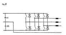
- Fig. 9 an inverter for 3-phase supply to the grid 8. All three inverters have a bipolar voltage link, the inputs E1 to E3 and the outputs 6, 7 as described above. Since inverters of this type are known per se, further explanations do not appear to be necessary.
- the magnetic coupling of the windings W1 and W2 is preferably obtained by winding them on top of each other or successively onto a common core as needed. They preferably have the same number of turns and become in the schematically illustrated arrangement Fig. 2 and 4 suitably wound with opposite winding sense on the core 16 in order to obtain the correct current directions in the loading and unloading operations.
- the invention is not limited to the described embodiments, which can be modified in many ways. This applies in particular to the extent that the inverters 3 and the DC-DC converters 2 can be manufactured and sold as separate components, although they are preferably produced and sold as a finished unit, as can be seen from the drawings. Therefore, the invention relates not only to the combination of a DC-DC converter 2 and an inverter 3, but also the DC-DC converter 2 alone. Furthermore, it is clear that in the above description, only the necessary components for understanding the invention have been described and in particular the necessary and known control organs, MPP regulations, etc. may be additionally present. It will also be understood that the various features may be applied in combinations other than those described and illustrated.
Claims (11)
- Dispositif pour l'injection d'énergie électrique dans un réseau de distribution d'énergie (8), comprenant un convertisseur de tenson continue (2) prévu pour la connexion à un générateur de tension continue (1) et un onduleur (3) relié à ce convertisseur, prévu pour la connexion au réseau de distribution d'énergie (8) et qui comporte un circuit intermédiaire de tension bipolaire comportant deux condensateurs (C1, C2) montés en série, qui sont reliés entre eux au niveau d'une connexion de terre (E3) reliée à une sortie négative (5) du générateur de tension continue (1), dans lequel le convertisseur de tension continue (2) comporte au moins deux diodes, un interrupteur et une réactance à accumulation, laquelle comprend un premier enroulement (W1) et un second enroulement (W2), dans lequel ces deux enroulements (W1, W2) sont couplés magnétiquement l'un à l'autre et sont reliés l'un à l'autre par une liaison galvanique, chacun par une de ses extrémités de connexion, de sorte que, dans un premier état de commutation, le premier enroulement (W1) est chargé par le générateur de tension continue (1) et le second enroulement (W2) est chargé par l'intermédiaire du premier enroulement (W1) sous l'effet du couplage magnétique, et que, dans un second état de commutation, les deux enroulements (W1, W2) sont déchargés, chacun à son tour par l'intermédiaire de celui des deux condensateurs (C1, C2), qui leur sont associés et de la diode qui leur est associée,
caractérisé en ce que
une première connexion du premier enroulement (W1) est reliée à un premier point de jonction (22) pourvu d'un premier interrupteur (S5), et une seconde connexion du premier enroulement (W1) est reliée à un second point de jonction (23) pourvu d'un second interrupteur (S6) de sorte que le premier enroulement (W1) forme avec les deux interrupteurs (S5, S6) un premier circuit connecté à des sorties correspondantes (4, 5) du générateur de tension continue (1) et est par ailleurs intercalé dans un second circuit qui, en partant de la connexion de terre (E3), par l'intermédiaire d'une première diode (D6), du premier point de jonction (22), du premier enroulement (W1), du second point de jonction (23), d'une deuxième diode (D7) et du condensateur (1) associé, ramène à la connexion de terre (E3), et en ce que le second enroulement (W2) est intercalé dans un troisième circuit qui, en partant de la connexion de terre (E3), par l'intermédiaire du condensateur (C2) associé, d'une troisième diode (D8) et du second enroulement (W2), ramène à la connexion de terre (E3). - Dispositif pour l'injection d'énergie électrique dans un réseau de distribution d'énergie (8), comprenant un convertisseur de tenson continue (2) prévu pour la connexion à un générateur de tension continue (1) et un onduleur (3) relié à ce convertisseur, prévu pour la connexion au réseau de distribution d'énergie (8) et qui comporte un circuit intermédiaire de tension bipolaire comportant deux condensateurs (C1, C2) montés en série, qui sont reliés entre eux au niveau d'une connexion de terre (E3) reliée à une sortie négative (5) du générateur de tension continue (1), dans lequel le convertisseur de tension continue (2) comporte au moins deux diodes, un interrupteur (S4) et une réactance à accumulation (25), laquelle comprend un premier enroulement (W1) et un second enroulement (W2), dans lequel ces deux enroulements (W1, W2) sont couplés magnétiquement l'un à l'autre et reliés l'un à l'autre par une liaison galvanique, chacun par une de ses extrémités de connexion, de sorte que, dans un premier état de commutation, le premier enroulement (W1) est chargé par le générateur de tension continue (1) et le second enroulement (W2) est chargé par l'intermédiaire du premier enroulement (W1) sous l'effet du couplage magnétique, et que, dans un second état de commutation, les deux enroulements (W1, W2) sont déchargés, chacun par l'intermédiaire de celui des deux condensateurs (C1, C2), qui leur sont associés, et de la diode (D4, D5) qui leur est associée,
caractérisé en ce que
un des enroulements (W1) est divisé et doté d'une prise d'enroulement (26) connectée à l'interrupteur (S4) de sorte que seule une première partie (W11) du premier enroulement (W1), qui est définie par cette prise (26), se trouve dans un premier de trois circuits, tandis qu'une seconde partie (W11 + W12) du premier enroulement (W1) est disposée dans un deuxième des trois circuits, les deux enroulements (W1, W2) étant bobinés sur un noyau commun. - Dispositif selon la revendication 1,
caractérisé en ce que
un des enroulements (W1) est divisé et doté d'une prise d'enroulement (22) connectée à un des points de jonction (21, 23) de sorte que seule une première partie (W11) du premier enroulement (W1), qui est définie par cette prise (22), se trouve dans le premier circuit, tandis qu'une seconde partie (W11 + W12) du premier enroulement (W1) est disposée dans le deuxième circuit. - Dispositif selon la revendication 1,
caractérisé en ce que
les deux enroulements (W1, W2) sont bobinés sur un noyau commun (16). - Dispositif selon la revendication 4,
caractérisé en ce que
les enroulements (W1, W2) sont bobinés sur le noyau (16) avec des sens de bobinage opposés. - Dispositif selon l'une des revendications 1 à 5,
caractérisé en ce que
les deux enroulements (W1, W2) comportent les mêmes nombres de tours. - Dispositif selon l'une des revendications 1 à 6,
caractérisé en ce que
l'onduleur (3) est formé par un onduleur comportant un demi-pont. - Dispositif selon l'une des revendications 1 à 6,
caractérisé en ce que
l'onduleur (3) est formé par un onduleur comportant un demi-pont dans un montage à 3 points (Fig. 7). - Dispositif selon l'une des revendications 1 à 6,
caractérisé en ce que
l'onduleur (3) est formé par un onduleur comportant un demi-pont dans un montage à 3 points avec un point central (Fig. 8). - Dispositif selon l'une des revendications 1 à 6,
caractérisé en ce que
l'onduleur (3) est formé pour l'injection de l'énergie électrique en monophasé ou en triphasé dans le réseau de distribution d'énergie (8) (Fig. 2 à 8 ou Fig. 9). - Dispositif selon la revendication 10,
caractérisé en ce que
le convertisseur de tension continue (2) est lié à l'onduleur (3) pour former une unité modulaire.
Applications Claiming Priority (2)
| Application Number | Priority Date | Filing Date | Title |
|---|---|---|---|
| DE102007028077A DE102007028077B4 (de) | 2007-06-15 | 2007-06-15 | Vorrichtung zur Einspeisung elektrischer Energie in ein Energieversorgungsnetz und Gleichspannungswandler für eine solche Vorrichtung |
| PCT/DE2008/000619 WO2008151587A1 (fr) | 2007-06-15 | 2008-04-12 | Dispositif d'alimentation électrique dans un réseau d'alimentation électrique et convertisseur de tension continue destiné à un tel dispositif |
Publications (2)
| Publication Number | Publication Date |
|---|---|
| EP2027647A1 EP2027647A1 (fr) | 2009-02-25 |
| EP2027647B1 true EP2027647B1 (fr) | 2011-09-28 |
Family
ID=39764741
Family Applications (1)
| Application Number | Title | Priority Date | Filing Date |
|---|---|---|---|
| EP08757930A Not-in-force EP2027647B1 (fr) | 2007-06-15 | 2008-04-12 | Dispositif d'alimentation électrique dans un réseau d'alimentation électrique et convertisseur de tension continue destiné à un tel dispositif |
Country Status (8)
| Country | Link |
|---|---|
| US (1) | US8116103B2 (fr) |
| EP (1) | EP2027647B1 (fr) |
| JP (1) | JP5097818B2 (fr) |
| KR (1) | KR101050294B1 (fr) |
| CN (1) | CN101682260B (fr) |
| AT (1) | ATE526721T1 (fr) |
| DE (1) | DE102007028077B4 (fr) |
| WO (1) | WO2008151587A1 (fr) |
Families Citing this family (72)
| Publication number | Priority date | Publication date | Assignee | Title |
|---|---|---|---|---|
| US10693415B2 (en) | 2007-12-05 | 2020-06-23 | Solaredge Technologies Ltd. | Testing of a photovoltaic panel |
| US11881814B2 (en) | 2005-12-05 | 2024-01-23 | Solaredge Technologies Ltd. | Testing of a photovoltaic panel |
| US8013472B2 (en) | 2006-12-06 | 2011-09-06 | Solaredge, Ltd. | Method for distributed power harvesting using DC power sources |
| US11855231B2 (en) | 2006-12-06 | 2023-12-26 | Solaredge Technologies Ltd. | Distributed power harvesting systems using DC power sources |
| US8384243B2 (en) | 2007-12-04 | 2013-02-26 | Solaredge Technologies Ltd. | Distributed power harvesting systems using DC power sources |
| US11569659B2 (en) | 2006-12-06 | 2023-01-31 | Solaredge Technologies Ltd. | Distributed power harvesting systems using DC power sources |
| US8947194B2 (en) | 2009-05-26 | 2015-02-03 | Solaredge Technologies Ltd. | Theft detection and prevention in a power generation system |
| US8618692B2 (en) | 2007-12-04 | 2013-12-31 | Solaredge Technologies Ltd. | Distributed power system using direct current power sources |
| US11687112B2 (en) | 2006-12-06 | 2023-06-27 | Solaredge Technologies Ltd. | Distributed power harvesting systems using DC power sources |
| US8319483B2 (en) | 2007-08-06 | 2012-11-27 | Solaredge Technologies Ltd. | Digital average input current control in power converter |
| US8473250B2 (en) | 2006-12-06 | 2013-06-25 | Solaredge, Ltd. | Monitoring of distributed power harvesting systems using DC power sources |
| US9112379B2 (en) | 2006-12-06 | 2015-08-18 | Solaredge Technologies Ltd. | Pairing of components in a direct current distributed power generation system |
| US11296650B2 (en) | 2006-12-06 | 2022-04-05 | Solaredge Technologies Ltd. | System and method for protection during inverter shutdown in distributed power installations |
| US11728768B2 (en) | 2006-12-06 | 2023-08-15 | Solaredge Technologies Ltd. | Pairing of components in a direct current distributed power generation system |
| US11309832B2 (en) | 2006-12-06 | 2022-04-19 | Solaredge Technologies Ltd. | Distributed power harvesting systems using DC power sources |
| US8816535B2 (en) | 2007-10-10 | 2014-08-26 | Solaredge Technologies, Ltd. | System and method for protection during inverter shutdown in distributed power installations |
| US9088178B2 (en) | 2006-12-06 | 2015-07-21 | Solaredge Technologies Ltd | Distributed power harvesting systems using DC power sources |
| US11888387B2 (en) | 2006-12-06 | 2024-01-30 | Solaredge Technologies Ltd. | Safety mechanisms, wake up and shutdown methods in distributed power installations |
| US8319471B2 (en) | 2006-12-06 | 2012-11-27 | Solaredge, Ltd. | Battery power delivery module |
| US11735910B2 (en) | 2006-12-06 | 2023-08-22 | Solaredge Technologies Ltd. | Distributed power system using direct current power sources |
| US8963369B2 (en) | 2007-12-04 | 2015-02-24 | Solaredge Technologies Ltd. | Distributed power harvesting systems using DC power sources |
| US9130401B2 (en) | 2006-12-06 | 2015-09-08 | Solaredge Technologies Ltd. | Distributed power harvesting systems using DC power sources |
| DE102007029767B3 (de) * | 2007-06-22 | 2008-12-24 | Fraunhofer-Gesellschaft zur Förderung der angewandten Forschung e.V. | Wechselrichter |
| WO2009072076A2 (fr) | 2007-12-05 | 2009-06-11 | Solaredge Technologies Ltd. | Détection de courant sur un transistor mosfet |
| WO2009072075A2 (fr) | 2007-12-05 | 2009-06-11 | Solaredge Technologies Ltd. | Procédé de suivi de puissance d'un système photovoltaïque |
| EP2232690B1 (fr) | 2007-12-05 | 2016-08-31 | Solaredge Technologies Ltd. | Onduleurs connectés en parallèle |
| JP2011507465A (ja) | 2007-12-05 | 2011-03-03 | ソラレッジ テクノロジーズ リミテッド | 分散型電力据付における安全機構、ウェークアップ方法およびシャットダウン方法 |
| US11264947B2 (en) | 2007-12-05 | 2022-03-01 | Solaredge Technologies Ltd. | Testing of a photovoltaic panel |
| WO2009118683A2 (fr) | 2008-03-24 | 2009-10-01 | Solaredge Technolgies Ltd. | Commutation sous tension nulle |
| JP4444343B2 (ja) * | 2008-04-25 | 2010-03-31 | 本田技研工業株式会社 | 燃料電池車両 |
| EP2294669B8 (fr) | 2008-05-05 | 2016-12-07 | Solaredge Technologies Ltd. | Circuit combinateur de puissance de courant continu |
| EP2280469B1 (fr) * | 2009-07-30 | 2016-07-06 | Nxp B.V. | Unité photovoltaïque, son convertisseur cc/cc, et son procédé de fonctionnement |
| JP4764499B2 (ja) * | 2009-08-05 | 2011-09-07 | 本田技研工業株式会社 | Dc/dcコンバータ及びそのdc/dcコンバータを備えた電力供給システム |
| US8710699B2 (en) | 2009-12-01 | 2014-04-29 | Solaredge Technologies Ltd. | Dual use photovoltaic system |
| US8558484B2 (en) | 2009-12-28 | 2013-10-15 | Power Integrations, Inc. | Power converter having a switch coupled between windings |
| US8933649B2 (en) * | 2009-12-28 | 2015-01-13 | Power Integrations, Inc. | Power converter having a switch coupled between windings |
| US8766696B2 (en) | 2010-01-27 | 2014-07-01 | Solaredge Technologies Ltd. | Fast voltage level shifter circuit |
| DE102010006124B4 (de) * | 2010-01-29 | 2015-04-09 | Platinum Gmbh | Schaltungsanordnung mit einem Hochsetzsteller und Wechselrichterschaltung mit einer solchen Schaltungsanordnung |
| CN102255538B (zh) * | 2010-05-19 | 2014-03-12 | 力博特公司 | 一种t型三电平逆变电路 |
| EP2605365A1 (fr) * | 2010-08-11 | 2013-06-19 | Ingeteam Power Technology, S.A. | Système de gestion pour systèmes de production d'énergie de ressources variables |
| DE102010048541A1 (de) * | 2010-10-14 | 2012-04-19 | Converteam Gmbh | Verfahren und elektrische Schaltung zum Testen eines an ein elektrisches Energieversorgungsnetz anschließbaren Energieerzeugers oder Energieverbrauchers |
| US10673229B2 (en) | 2010-11-09 | 2020-06-02 | Solaredge Technologies Ltd. | Arc detection and prevention in a power generation system |
| US10230310B2 (en) | 2016-04-05 | 2019-03-12 | Solaredge Technologies Ltd | Safety switch for photovoltaic systems |
| US10673222B2 (en) | 2010-11-09 | 2020-06-02 | Solaredge Technologies Ltd. | Arc detection and prevention in a power generation system |
| GB2485527B (en) | 2010-11-09 | 2012-12-19 | Solaredge Technologies Ltd | Arc detection and prevention in a power generation system |
| GB2486408A (en) | 2010-12-09 | 2012-06-20 | Solaredge Technologies Ltd | Disconnection of a string carrying direct current |
| GB2483317B (en) | 2011-01-12 | 2012-08-22 | Solaredge Technologies Ltd | Serially connected inverters |
| EP2493062B1 (fr) | 2011-02-28 | 2015-04-15 | SEMIKRON Elektronik GmbH & Co. KG | Cellule de convertisseur CC-CC, circuit convertisseur ayant une capacité de retour monté à partir de celle-ci et son procédé de fonctionnement |
| DE202011102068U1 (de) * | 2011-06-07 | 2012-09-10 | Voltwerk Electronics Gmbh | Hochsetzsteller |
| US9462724B2 (en) * | 2011-06-27 | 2016-10-04 | Bloom Energy Corporation | Convergent energized IT apparatus for commercial use |
| US9059600B2 (en) | 2011-06-27 | 2015-06-16 | Bloom Energy Corporation | Convergent energized IT apparatus for residential use |
| DE102011052768A1 (de) * | 2011-08-17 | 2013-02-21 | Sma Solar Technology Ag | Wechselrichter mit gekoppelten Induktivitäten |
| US8570005B2 (en) | 2011-09-12 | 2013-10-29 | Solaredge Technologies Ltd. | Direct current link circuit |
| GB2498365A (en) | 2012-01-11 | 2013-07-17 | Solaredge Technologies Ltd | Photovoltaic module |
| GB2498791A (en) | 2012-01-30 | 2013-07-31 | Solaredge Technologies Ltd | Photovoltaic panel circuitry |
| US9853565B2 (en) | 2012-01-30 | 2017-12-26 | Solaredge Technologies Ltd. | Maximized power in a photovoltaic distributed power system |
| GB2498790A (en) | 2012-01-30 | 2013-07-31 | Solaredge Technologies Ltd | Maximising power in a photovoltaic distributed power system |
| GB2499991A (en) | 2012-03-05 | 2013-09-11 | Solaredge Technologies Ltd | DC link circuit for photovoltaic array |
| EP3499695A1 (fr) | 2012-05-25 | 2019-06-19 | Solaredge Technologies Ltd. | Circuit pour sources interconnectées de courant continu |
| US10115841B2 (en) | 2012-06-04 | 2018-10-30 | Solaredge Technologies Ltd. | Integrated photovoltaic panel circuitry |
| US9548619B2 (en) | 2013-03-14 | 2017-01-17 | Solaredge Technologies Ltd. | Method and apparatus for storing and depleting energy |
| US9941813B2 (en) | 2013-03-14 | 2018-04-10 | Solaredge Technologies Ltd. | High frequency multi-level inverter |
| EP3506370B1 (fr) | 2013-03-15 | 2023-12-20 | Solaredge Technologies Ltd. | Mécanisme de dérivation |
| US9318974B2 (en) | 2014-03-26 | 2016-04-19 | Solaredge Technologies Ltd. | Multi-level inverter with flying capacitor topology |
| KR101655018B1 (ko) * | 2015-03-13 | 2016-09-07 | 성균관대학교산학협력단 | 저압직류 배전계통의 전압 불평형 제어 시스템 및 방법 |
| FR3043281B1 (fr) * | 2015-10-30 | 2017-12-08 | Peugeot Citroen Automobiles Sa | Dispositif de controle actif pour un circuit electrique a convertisseur dc/dc et stockeur d’energie electrique montes en serie |
| US11018623B2 (en) | 2016-04-05 | 2021-05-25 | Solaredge Technologies Ltd. | Safety switch for photovoltaic systems |
| US11177663B2 (en) | 2016-04-05 | 2021-11-16 | Solaredge Technologies Ltd. | Chain of power devices |
| US10495145B2 (en) | 2016-04-22 | 2019-12-03 | Ingersoll-Rand Company | Active magnetic bearing controller |
| US10686378B2 (en) * | 2016-12-16 | 2020-06-16 | Futurewei Technologies, Inc. | High-efficiency regulated buck-boost converter |
| DE102017212462A1 (de) * | 2017-07-20 | 2019-01-24 | Siemens Aktiengesellschaft | Galvanisch gekoppelter elektrischer Wandler |
| DE102020110055A1 (de) | 2020-04-09 | 2021-10-14 | Sma Solar Technology Ag | Wechselrichter und verfahren zum betrieb eines wechselrichters |
Family Cites Families (21)
| Publication number | Priority date | Publication date | Assignee | Title |
|---|---|---|---|---|
| JPS6051458A (ja) * | 1983-08-31 | 1985-03-22 | Toshiba Corp | Dc−dcコンバ−タ |
| US5400235A (en) * | 1992-08-07 | 1995-03-21 | International Business Machines Corp. | High frequency energy saving DC to DC power converter |
| JP2630221B2 (ja) * | 1993-10-08 | 1997-07-16 | 日本電気株式会社 | Dc−dcコンバータ |
| JP3151130B2 (ja) * | 1995-08-11 | 2001-04-03 | デンセイ・ラムダ株式会社 | バッテリー電源を共用化したハーフブリッジ型インバータの±直流2電源の昇圧チョッパ回路 |
| DE19642522C1 (de) * | 1996-10-15 | 1998-04-23 | Dietrich Karschny | Wechselrichter |
| DE19732218C1 (de) * | 1997-07-26 | 1999-03-18 | Dirk Schekulin | Transformatorlose Wechselrichter-Schaltungsanordnung |
| CA2227747A1 (fr) * | 1998-01-23 | 1999-07-23 | Gary Arthur Edwards | Regulateur devolteur a sorties multiples |
| US6115273A (en) * | 1998-07-09 | 2000-09-05 | Illinois Tool Works Inc. | Power converter with low loss switching |
| DE10221592A1 (de) * | 2002-05-15 | 2003-12-04 | Fraunhofer Ges Forschung | Wechselrichter sowie Verfahren zum Umwandeln einer elektrischen Gleichspannung in einen Wechselstrom |
| DE10225020A1 (de) * | 2002-06-06 | 2003-12-24 | Sma Regelsysteme Gmbh | Schaltungsanordnung, Verfahren zur Wechselstromerzeugung |
| JP2005033867A (ja) * | 2003-07-08 | 2005-02-03 | Honda Motor Co Ltd | 電力制御装置及び電力制御方法 |
| EP1544992A1 (fr) * | 2003-12-16 | 2005-06-22 | ABB Schweiz AG | Circuit convertisseur avec deux convertisseurs partiels |
| DE102004030912B3 (de) * | 2004-06-25 | 2006-01-19 | Sma Technologie Ag | Verfahren zum Umwandeln einer elektrischen Gleichspannung einer Gleichspannungsquelle, insbesondere einer Photovoltaik-Gleichspannungsquelle in eine Wechselspannung |
| DE102004037446B4 (de) * | 2004-08-02 | 2006-11-02 | Conergy Ag | Trafoloser Wechselrichter für solare Netzeinspeisung |
| US7319313B2 (en) * | 2005-08-10 | 2008-01-15 | Xantrex Technology, Inc. | Photovoltaic DC-to-AC power converter and control method |
| TW200709544A (en) * | 2005-08-29 | 2007-03-01 | Ind Tech Res Inst | Transformer-free power conversion circuit for parallel connection with commercial electricity system |
| US20070053217A1 (en) | 2005-09-02 | 2007-03-08 | Lear Corporation | Converter for automotive use |
| US20090003024A1 (en) * | 2005-10-24 | 2009-01-01 | Conergy Ag | Inverter |
| DE102006012164B4 (de) | 2005-12-23 | 2009-12-17 | Fraunhofer-Gesellschaft zur Förderung der angewandten Forschung e.V. | Schaltungsanordnung zur Erzeugung einer Wechselspannung oder eines Wechselstroms |
| EP1971018A1 (fr) * | 2007-03-13 | 2008-09-17 | SMA Solar Technology AG | Circuit destiné à la transformation sans transformateur d'une tension continue en tension alternative avec deux convertisseurs à courant continu et un onduleur |
| TWI373906B (en) * | 2009-04-06 | 2012-10-01 | Ablerex Electronics Co Ltd | Dc/ac inverter |
-
2007
- 2007-06-15 DE DE102007028077A patent/DE102007028077B4/de not_active Expired - Fee Related
-
2008
- 2008-04-12 JP JP2010511482A patent/JP5097818B2/ja not_active Expired - Fee Related
- 2008-04-12 EP EP08757930A patent/EP2027647B1/fr not_active Not-in-force
- 2008-04-12 AT AT08757930T patent/ATE526721T1/de active
- 2008-04-12 WO PCT/DE2008/000619 patent/WO2008151587A1/fr active Application Filing
- 2008-04-12 KR KR1020097004129A patent/KR101050294B1/ko not_active IP Right Cessation
- 2008-04-12 CN CN2008800204177A patent/CN101682260B/zh not_active Expired - Fee Related
- 2008-04-12 US US12/309,425 patent/US8116103B2/en not_active Expired - Fee Related
Also Published As
| Publication number | Publication date |
|---|---|
| DE102007028077B4 (de) | 2009-04-16 |
| JP5097818B2 (ja) | 2012-12-12 |
| US20100085788A1 (en) | 2010-04-08 |
| KR101050294B1 (ko) | 2011-07-19 |
| ATE526721T1 (de) | 2011-10-15 |
| EP2027647A1 (fr) | 2009-02-25 |
| DE102007028077A1 (de) | 2008-12-24 |
| WO2008151587A1 (fr) | 2008-12-18 |
| US8116103B2 (en) | 2012-02-14 |
| CN101682260B (zh) | 2013-05-15 |
| JP2010530205A (ja) | 2010-09-02 |
| KR20090085023A (ko) | 2009-08-06 |
| CN101682260A (zh) | 2010-03-24 |
Similar Documents
| Publication | Publication Date | Title |
|---|---|---|
| EP2027647B1 (fr) | Dispositif d'alimentation électrique dans un réseau d'alimentation électrique et convertisseur de tension continue destiné à un tel dispositif | |
| EP2067230B1 (fr) | Dispositif destiné à l'alimentation en énergie électrique d'un réseau d'alimentation en énergie et convertisseur pour un tel dispositif | |
| EP2030299B1 (fr) | Onduleur destiné à injecter de l'énergie électrique dans un réseau de distribution d'énergie | |
| EP2026457A1 (fr) | Onduleur avec deux circuits intermédiaires | |
| DE102006012164B4 (de) | Schaltungsanordnung zur Erzeugung einer Wechselspannung oder eines Wechselstroms | |
| EP2026456A1 (fr) | Onduleur | |
| WO2007025702A2 (fr) | Dispositif de commande conçu pour un convertisseur de tension, et procede | |
| DE102019106485B4 (de) | Weissach-Gleichrichteranordnung | |
| DE102018008603A1 (de) | Schaltungsanordnung und Verfahren zum Laden einer Batterieanordnung mit mehreren Batteriemodulen | |
| DE102017212462A1 (de) | Galvanisch gekoppelter elektrischer Wandler | |
| EP0521901B1 (fr) | Dispositif d'alimentation ininterrompue en courant electrique | |
| DE4426017C2 (de) | Stromversorgungsgerät, insbesondere Batterie-Ladegerät für Elektrofahrzeuge oder dergleichen | |
| DE102013105098B4 (de) | Integrierter Solar-/Batteriewechselrichter | |
| DE102013212692A1 (de) | Energiespeichereinrichtung mit Gleichspannungsversorgungsschaltung | |
| DE102020104252A1 (de) | Leistungswandler | |
| EP2523339B1 (fr) | Procédé et dispositif de génération d'énergie au moyen d'une installation photovoltaïque avec une compensation d'énergie entre les branches des générateurs photovoltaïques | |
| EP2826126B1 (fr) | Dispositif électronique de puissance comportant une symétrisation d'un n ud de tension dans le circuit intermédiaire | |
| DE102007029767B3 (de) | Wechselrichter | |
| DE202020101549U1 (de) | Schaltungsanordnung mit mehreren Leistungselektronikmodulen | |
| DE102010010781A1 (de) | Anordnung aus Wechselrichter und elektrischer Maschine | |
| DE102011115728A1 (de) | Verfahren zum Betreiben eines Wechselrichters und Wechselrichterschaltung |
Legal Events
| Date | Code | Title | Description |
|---|---|---|---|
| PUAI | Public reference made under article 153(3) epc to a published international application that has entered the european phase |
Free format text: ORIGINAL CODE: 0009012 |
|
| 17P | Request for examination filed |
Effective date: 20081229 |
|
| AK | Designated contracting states |
Kind code of ref document: A1 Designated state(s): AT BE BG CH CY CZ DE DK EE ES FI FR GB GR HR HU IE IS IT LI LT LU LV MC MT NL NO PL PT RO SE SI SK TR |
|
| AX | Request for extension of the european patent |
Extension state: AL BA MK RS |
|
| GRAP | Despatch of communication of intention to grant a patent |
Free format text: ORIGINAL CODE: EPIDOSNIGR1 |
|
| DAX | Request for extension of the european patent (deleted) | ||
| GRAS | Grant fee paid |
Free format text: ORIGINAL CODE: EPIDOSNIGR3 |
|
| GRAA | (expected) grant |
Free format text: ORIGINAL CODE: 0009210 |
|
| AK | Designated contracting states |
Kind code of ref document: B1 Designated state(s): AT BE BG CH CY CZ DE DK EE ES FI FR GB GR HR HU IE IS IT LI LT LU LV MC MT NL NO PL PT RO SE SI SK TR |
|
| REG | Reference to a national code |
Ref country code: GB Ref legal event code: FG4D Free format text: NOT ENGLISH |
|
| REG | Reference to a national code |
Ref country code: CH Ref legal event code: EP |
|
| REG | Reference to a national code |
Ref country code: IE Ref legal event code: FG4D |
|
| REG | Reference to a national code |
Ref country code: DE Ref legal event code: R096 Ref document number: 502008005036 Country of ref document: DE Effective date: 20111124 |
|
| REG | Reference to a national code |
Ref country code: NL Ref legal event code: VDEP Effective date: 20110928 |
|
| PG25 | Lapsed in a contracting state [announced via postgrant information from national office to epo] |
Ref country code: SE Free format text: LAPSE BECAUSE OF FAILURE TO SUBMIT A TRANSLATION OF THE DESCRIPTION OR TO PAY THE FEE WITHIN THE PRESCRIBED TIME-LIMIT Effective date: 20110928 Ref country code: LT Free format text: LAPSE BECAUSE OF FAILURE TO SUBMIT A TRANSLATION OF THE DESCRIPTION OR TO PAY THE FEE WITHIN THE PRESCRIBED TIME-LIMIT Effective date: 20110928 Ref country code: NO Free format text: LAPSE BECAUSE OF FAILURE TO SUBMIT A TRANSLATION OF THE DESCRIPTION OR TO PAY THE FEE WITHIN THE PRESCRIBED TIME-LIMIT Effective date: 20111228 Ref country code: HR Free format text: LAPSE BECAUSE OF FAILURE TO SUBMIT A TRANSLATION OF THE DESCRIPTION OR TO PAY THE FEE WITHIN THE PRESCRIBED TIME-LIMIT Effective date: 20110928 Ref country code: FI Free format text: LAPSE BECAUSE OF FAILURE TO SUBMIT A TRANSLATION OF THE DESCRIPTION OR TO PAY THE FEE WITHIN THE PRESCRIBED TIME-LIMIT Effective date: 20110928 |
|
| LTIE | Lt: invalidation of european patent or patent extension |
Effective date: 20110928 |
|
| PG25 | Lapsed in a contracting state [announced via postgrant information from national office to epo] |
Ref country code: CY Free format text: LAPSE BECAUSE OF FAILURE TO SUBMIT A TRANSLATION OF THE DESCRIPTION OR TO PAY THE FEE WITHIN THE PRESCRIBED TIME-LIMIT Effective date: 20110928 Ref country code: GR Free format text: LAPSE BECAUSE OF FAILURE TO SUBMIT A TRANSLATION OF THE DESCRIPTION OR TO PAY THE FEE WITHIN THE PRESCRIBED TIME-LIMIT Effective date: 20111229 Ref country code: LV Free format text: LAPSE BECAUSE OF FAILURE TO SUBMIT A TRANSLATION OF THE DESCRIPTION OR TO PAY THE FEE WITHIN THE PRESCRIBED TIME-LIMIT Effective date: 20110928 Ref country code: SI Free format text: LAPSE BECAUSE OF FAILURE TO SUBMIT A TRANSLATION OF THE DESCRIPTION OR TO PAY THE FEE WITHIN THE PRESCRIBED TIME-LIMIT Effective date: 20110928 |
|
| REG | Reference to a national code |
Ref country code: IE Ref legal event code: FD4D |
|
| PG25 | Lapsed in a contracting state [announced via postgrant information from national office to epo] |
Ref country code: CZ Free format text: LAPSE BECAUSE OF FAILURE TO SUBMIT A TRANSLATION OF THE DESCRIPTION OR TO PAY THE FEE WITHIN THE PRESCRIBED TIME-LIMIT Effective date: 20110928 Ref country code: IS Free format text: LAPSE BECAUSE OF FAILURE TO SUBMIT A TRANSLATION OF THE DESCRIPTION OR TO PAY THE FEE WITHIN THE PRESCRIBED TIME-LIMIT Effective date: 20120128 Ref country code: SK Free format text: LAPSE BECAUSE OF FAILURE TO SUBMIT A TRANSLATION OF THE DESCRIPTION OR TO PAY THE FEE WITHIN THE PRESCRIBED TIME-LIMIT Effective date: 20110928 |
|
| PG25 | Lapsed in a contracting state [announced via postgrant information from national office to epo] |
Ref country code: NL Free format text: LAPSE BECAUSE OF FAILURE TO SUBMIT A TRANSLATION OF THE DESCRIPTION OR TO PAY THE FEE WITHIN THE PRESCRIBED TIME-LIMIT Effective date: 20110928 Ref country code: PT Free format text: LAPSE BECAUSE OF FAILURE TO SUBMIT A TRANSLATION OF THE DESCRIPTION OR TO PAY THE FEE WITHIN THE PRESCRIBED TIME-LIMIT Effective date: 20120130 Ref country code: RO Free format text: LAPSE BECAUSE OF FAILURE TO SUBMIT A TRANSLATION OF THE DESCRIPTION OR TO PAY THE FEE WITHIN THE PRESCRIBED TIME-LIMIT Effective date: 20110928 Ref country code: EE Free format text: LAPSE BECAUSE OF FAILURE TO SUBMIT A TRANSLATION OF THE DESCRIPTION OR TO PAY THE FEE WITHIN THE PRESCRIBED TIME-LIMIT Effective date: 20110928 |
|
| PG25 | Lapsed in a contracting state [announced via postgrant information from national office to epo] |
Ref country code: DK Free format text: LAPSE BECAUSE OF FAILURE TO SUBMIT A TRANSLATION OF THE DESCRIPTION OR TO PAY THE FEE WITHIN THE PRESCRIBED TIME-LIMIT Effective date: 20110928 Ref country code: IE Free format text: LAPSE BECAUSE OF FAILURE TO SUBMIT A TRANSLATION OF THE DESCRIPTION OR TO PAY THE FEE WITHIN THE PRESCRIBED TIME-LIMIT Effective date: 20110928 |
|
| PLBE | No opposition filed within time limit |
Free format text: ORIGINAL CODE: 0009261 |
|
| STAA | Information on the status of an ep patent application or granted ep patent |
Free format text: STATUS: NO OPPOSITION FILED WITHIN TIME LIMIT |
|
| PG25 | Lapsed in a contracting state [announced via postgrant information from national office to epo] |
Ref country code: PL Free format text: LAPSE BECAUSE OF FAILURE TO SUBMIT A TRANSLATION OF THE DESCRIPTION OR TO PAY THE FEE WITHIN THE PRESCRIBED TIME-LIMIT Effective date: 20110928 |
|
| 26N | No opposition filed |
Effective date: 20120629 |
|
| REG | Reference to a national code |
Ref country code: DE Ref legal event code: R097 Ref document number: 502008005036 Country of ref document: DE Effective date: 20120629 |
|
| BERE | Be: lapsed |
Owner name: SMA SOLAR TECHNOLOGY A.G. Effective date: 20120430 |
|
| PG25 | Lapsed in a contracting state [announced via postgrant information from national office to epo] |
Ref country code: MC Free format text: LAPSE BECAUSE OF NON-PAYMENT OF DUE FEES Effective date: 20120430 |
|
| REG | Reference to a national code |
Ref country code: CH Ref legal event code: PL |
|
| GBPC | Gb: european patent ceased through non-payment of renewal fee |
Effective date: 20120412 |
|
| PG25 | Lapsed in a contracting state [announced via postgrant information from national office to epo] |
Ref country code: CH Free format text: LAPSE BECAUSE OF NON-PAYMENT OF DUE FEES Effective date: 20120430 Ref country code: GB Free format text: LAPSE BECAUSE OF NON-PAYMENT OF DUE FEES Effective date: 20120412 Ref country code: LI Free format text: LAPSE BECAUSE OF NON-PAYMENT OF DUE FEES Effective date: 20120430 Ref country code: BE Free format text: LAPSE BECAUSE OF NON-PAYMENT OF DUE FEES Effective date: 20120430 |
|
| PG25 | Lapsed in a contracting state [announced via postgrant information from national office to epo] |
Ref country code: ES Free format text: LAPSE BECAUSE OF FAILURE TO SUBMIT A TRANSLATION OF THE DESCRIPTION OR TO PAY THE FEE WITHIN THE PRESCRIBED TIME-LIMIT Effective date: 20120108 |
|
| PG25 | Lapsed in a contracting state [announced via postgrant information from national office to epo] |
Ref country code: BG Free format text: LAPSE BECAUSE OF FAILURE TO SUBMIT A TRANSLATION OF THE DESCRIPTION OR TO PAY THE FEE WITHIN THE PRESCRIBED TIME-LIMIT Effective date: 20111228 |
|
| PG25 | Lapsed in a contracting state [announced via postgrant information from national office to epo] |
Ref country code: MT Free format text: LAPSE BECAUSE OF FAILURE TO SUBMIT A TRANSLATION OF THE DESCRIPTION OR TO PAY THE FEE WITHIN THE PRESCRIBED TIME-LIMIT Effective date: 20110928 |
|
| REG | Reference to a national code |
Ref country code: DE Ref legal event code: R082 Ref document number: 502008005036 Country of ref document: DE |
|
| PG25 | Lapsed in a contracting state [announced via postgrant information from national office to epo] |
Ref country code: TR Free format text: LAPSE BECAUSE OF FAILURE TO SUBMIT A TRANSLATION OF THE DESCRIPTION OR TO PAY THE FEE WITHIN THE PRESCRIBED TIME-LIMIT Effective date: 20110928 |
|
| PG25 | Lapsed in a contracting state [announced via postgrant information from national office to epo] |
Ref country code: LU Free format text: LAPSE BECAUSE OF NON-PAYMENT OF DUE FEES Effective date: 20120412 |
|
| PG25 | Lapsed in a contracting state [announced via postgrant information from national office to epo] |
Ref country code: HU Free format text: LAPSE BECAUSE OF FAILURE TO SUBMIT A TRANSLATION OF THE DESCRIPTION OR TO PAY THE FEE WITHIN THE PRESCRIBED TIME-LIMIT Effective date: 20080412 |
|
| REG | Reference to a national code |
Ref country code: FR Ref legal event code: PLFP Year of fee payment: 8 |
|
| PGFP | Annual fee paid to national office [announced via postgrant information from national office to epo] |
Ref country code: DE Payment date: 20150422 Year of fee payment: 8 |
|
| PGFP | Annual fee paid to national office [announced via postgrant information from national office to epo] |
Ref country code: FR Payment date: 20150422 Year of fee payment: 8 Ref country code: IT Payment date: 20150424 Year of fee payment: 8 Ref country code: AT Payment date: 20150422 Year of fee payment: 8 |
|
| REG | Reference to a national code |
Ref country code: DE Ref legal event code: R119 Ref document number: 502008005036 Country of ref document: DE |
|
| REG | Reference to a national code |
Ref country code: AT Ref legal event code: MM01 Ref document number: 526721 Country of ref document: AT Kind code of ref document: T Effective date: 20160412 |
|
| REG | Reference to a national code |
Ref country code: FR Ref legal event code: ST Effective date: 20161230 |
|
| PG25 | Lapsed in a contracting state [announced via postgrant information from national office to epo] |
Ref country code: FR Free format text: LAPSE BECAUSE OF NON-PAYMENT OF DUE FEES Effective date: 20160502 Ref country code: DE Free format text: LAPSE BECAUSE OF NON-PAYMENT OF DUE FEES Effective date: 20161101 |
|
| PG25 | Lapsed in a contracting state [announced via postgrant information from national office to epo] |
Ref country code: AT Free format text: LAPSE BECAUSE OF NON-PAYMENT OF DUE FEES Effective date: 20160412 Ref country code: IT Free format text: LAPSE BECAUSE OF NON-PAYMENT OF DUE FEES Effective date: 20160412 |