EP2027647B1 - Device for feeding electric energy into a power grid and dc converter for such a device - Google Patents
Device for feeding electric energy into a power grid and dc converter for such a device Download PDFInfo
- Publication number
- EP2027647B1 EP2027647B1 EP08757930A EP08757930A EP2027647B1 EP 2027647 B1 EP2027647 B1 EP 2027647B1 EP 08757930 A EP08757930 A EP 08757930A EP 08757930 A EP08757930 A EP 08757930A EP 2027647 B1 EP2027647 B1 EP 2027647B1
- Authority
- EP
- European Patent Office
- Prior art keywords
- winding
- inverter
- windings
- direct voltage
- switch
- Prior art date
- Legal status (The legal status is an assumption and is not a legal conclusion. Google has not performed a legal analysis and makes no representation as to the accuracy of the status listed.)
- Not-in-force
Links
Images


Classifications
-
- H—ELECTRICITY
- H02—GENERATION; CONVERSION OR DISTRIBUTION OF ELECTRIC POWER
- H02M—APPARATUS FOR CONVERSION BETWEEN AC AND AC, BETWEEN AC AND DC, OR BETWEEN DC AND DC, AND FOR USE WITH MAINS OR SIMILAR POWER SUPPLY SYSTEMS; CONVERSION OF DC OR AC INPUT POWER INTO SURGE OUTPUT POWER; CONTROL OR REGULATION THEREOF
- H02M3/00—Conversion of dc power input into dc power output
- H02M3/02—Conversion of dc power input into dc power output without intermediate conversion into ac
- H02M3/04—Conversion of dc power input into dc power output without intermediate conversion into ac by static converters
- H02M3/10—Conversion of dc power input into dc power output without intermediate conversion into ac by static converters using discharge tubes with control electrode or semiconductor devices with control electrode
- H02M3/145—Conversion of dc power input into dc power output without intermediate conversion into ac by static converters using discharge tubes with control electrode or semiconductor devices with control electrode using devices of a triode or transistor type requiring continuous application of a control signal
- H02M3/155—Conversion of dc power input into dc power output without intermediate conversion into ac by static converters using discharge tubes with control electrode or semiconductor devices with control electrode using devices of a triode or transistor type requiring continuous application of a control signal using semiconductor devices only
-
- H—ELECTRICITY
- H02—GENERATION; CONVERSION OR DISTRIBUTION OF ELECTRIC POWER
- H02M—APPARATUS FOR CONVERSION BETWEEN AC AND AC, BETWEEN AC AND DC, OR BETWEEN DC AND DC, AND FOR USE WITH MAINS OR SIMILAR POWER SUPPLY SYSTEMS; CONVERSION OF DC OR AC INPUT POWER INTO SURGE OUTPUT POWER; CONTROL OR REGULATION THEREOF
- H02M7/00—Conversion of ac power input into dc power output; Conversion of dc power input into ac power output
- H02M7/42—Conversion of dc power input into ac power output without possibility of reversal
- H02M7/44—Conversion of dc power input into ac power output without possibility of reversal by static converters
- H02M7/48—Conversion of dc power input into ac power output without possibility of reversal by static converters using discharge tubes with control electrode or semiconductor devices with control electrode
-
- H—ELECTRICITY
- H02—GENERATION; CONVERSION OR DISTRIBUTION OF ELECTRIC POWER
- H02J—CIRCUIT ARRANGEMENTS OR SYSTEMS FOR SUPPLYING OR DISTRIBUTING ELECTRIC POWER; SYSTEMS FOR STORING ELECTRIC ENERGY
- H02J3/00—Circuit arrangements for ac mains or ac distribution networks
- H02J3/38—Arrangements for parallely feeding a single network by two or more generators, converters or transformers
- H02J3/381—Dispersed generators
-
- H—ELECTRICITY
- H02—GENERATION; CONVERSION OR DISTRIBUTION OF ELECTRIC POWER
- H02M—APPARATUS FOR CONVERSION BETWEEN AC AND AC, BETWEEN AC AND DC, OR BETWEEN DC AND DC, AND FOR USE WITH MAINS OR SIMILAR POWER SUPPLY SYSTEMS; CONVERSION OF DC OR AC INPUT POWER INTO SURGE OUTPUT POWER; CONTROL OR REGULATION THEREOF
- H02M7/00—Conversion of ac power input into dc power output; Conversion of dc power input into ac power output
- H02M7/02—Conversion of ac power input into dc power output without possibility of reversal
- H02M7/04—Conversion of ac power input into dc power output without possibility of reversal by static converters
- H02M7/12—Conversion of ac power input into dc power output without possibility of reversal by static converters using discharge tubes with control electrode or semiconductor devices with control electrode
- H02M7/145—Conversion of ac power input into dc power output without possibility of reversal by static converters using discharge tubes with control electrode or semiconductor devices with control electrode using devices of a thyratron or thyristor type requiring extinguishing means
- H02M7/155—Conversion of ac power input into dc power output without possibility of reversal by static converters using discharge tubes with control electrode or semiconductor devices with control electrode using devices of a thyratron or thyristor type requiring extinguishing means using semiconductor devices only
-
- H—ELECTRICITY
- H02—GENERATION; CONVERSION OR DISTRIBUTION OF ELECTRIC POWER
- H02J—CIRCUIT ARRANGEMENTS OR SYSTEMS FOR SUPPLYING OR DISTRIBUTING ELECTRIC POWER; SYSTEMS FOR STORING ELECTRIC ENERGY
- H02J2300/00—Systems for supplying or distributing electric power characterised by decentralized, dispersed, or local generation
- H02J2300/20—The dispersed energy generation being of renewable origin
- H02J2300/22—The renewable source being solar energy
- H02J2300/24—The renewable source being solar energy of photovoltaic origin
-
- H—ELECTRICITY
- H02—GENERATION; CONVERSION OR DISTRIBUTION OF ELECTRIC POWER
- H02M—APPARATUS FOR CONVERSION BETWEEN AC AND AC, BETWEEN AC AND DC, OR BETWEEN DC AND DC, AND FOR USE WITH MAINS OR SIMILAR POWER SUPPLY SYSTEMS; CONVERSION OF DC OR AC INPUT POWER INTO SURGE OUTPUT POWER; CONTROL OR REGULATION THEREOF
- H02M1/00—Details of apparatus for conversion
- H02M1/0067—Converter structures employing plural converter units, other than for parallel operation of the units on a single load
- H02M1/007—Plural converter units in cascade
-
- H—ELECTRICITY
- H02—GENERATION; CONVERSION OR DISTRIBUTION OF ELECTRIC POWER
- H02M—APPARATUS FOR CONVERSION BETWEEN AC AND AC, BETWEEN AC AND DC, OR BETWEEN DC AND DC, AND FOR USE WITH MAINS OR SIMILAR POWER SUPPLY SYSTEMS; CONVERSION OF DC OR AC INPUT POWER INTO SURGE OUTPUT POWER; CONTROL OR REGULATION THEREOF
- H02M7/00—Conversion of ac power input into dc power output; Conversion of dc power input into ac power output
- H02M7/42—Conversion of dc power input into ac power output without possibility of reversal
- H02M7/44—Conversion of dc power input into ac power output without possibility of reversal by static converters
- H02M7/48—Conversion of dc power input into ac power output without possibility of reversal by static converters using discharge tubes with control electrode or semiconductor devices with control electrode
- H02M7/483—Converters with outputs that each can have more than two voltages levels
- H02M7/487—Neutral point clamped inverters
-
- Y—GENERAL TAGGING OF NEW TECHNOLOGICAL DEVELOPMENTS; GENERAL TAGGING OF CROSS-SECTIONAL TECHNOLOGIES SPANNING OVER SEVERAL SECTIONS OF THE IPC; TECHNICAL SUBJECTS COVERED BY FORMER USPC CROSS-REFERENCE ART COLLECTIONS [XRACs] AND DIGESTS
- Y02—TECHNOLOGIES OR APPLICATIONS FOR MITIGATION OR ADAPTATION AGAINST CLIMATE CHANGE
- Y02E—REDUCTION OF GREENHOUSE GAS [GHG] EMISSIONS, RELATED TO ENERGY GENERATION, TRANSMISSION OR DISTRIBUTION
- Y02E10/00—Energy generation through renewable energy sources
- Y02E10/50—Photovoltaic [PV] energy
- Y02E10/56—Power conversion systems, e.g. maximum power point trackers
Definitions
- the invention relates to a device of the type specified in the preamble of claim 1 and a suitable DC-DC converter.
- DC generators For feeding electrical energy with DC generators such.
- B. photovoltaic or fuel cell systems is generated, in an AC network, in particular the public power grid (50/60 Hz), inverters of various kinds are used.
- a DC-DC converter is provided in most cases, which serves the purpose of converting the DC voltage supplied by the DC voltage generator into a required by the inverter or adapted to this DC voltage.
- a grounding of the type described is readily possible when DC-DC converters are used with transformers, which cause a galvanic separation of the DC side from the AC side.
- transformers regardless of whether mains transformers or high-frequency transformers are used, u. a. a reduction of the efficiency, sometimes considerable weights and sizes and / or an additional control effort result, which is why transformerless voltage transformers are preferred.
- transformerless DC-DC converters either make the desired grounding impossible, as this would result in the short circuiting of required switches, capacitors, or the like, or result in increased circuit complexity and other disadvantages.
- circuits which serve the purpose of reducing the unwanted leakage currents (eg. DE 10 2004 037 446 A1 . DE 102 21 592 A1 . DE 10 2004 030 912 B3 ).
- DE 10 2004 037 446 A1 . DE 102 21 592 A1 . DE 10 2004 030 912 B3 operated a solar generator in certain phases of the internal electric energy transport isolated from the grid.
- parasitic capacitances are only slightly reloaded, so that the potential of the solar generator with grid frequency sinusoidal and at a voltage amplitude of half the mains voltage corresponds, changes.
- High-frequency currents are then formed by the low voltage differences of the solar generator only between two switching cycles and by asymmetries during switching off. Capacitive leakage currents can therefore be greatly minimized in this way, but in principle not completely avoided.
- circuit arrangements are already known with which a solar generator can be grounded on one side despite the absence of a transformer. As a result, capacitive leakage currents are inherently prevented.
- One of these circuit arrangements ( DE 196 42 522 C1 ), however, requires five active switches, with one or two switches simultaneously switching to high-frequency and providing the average output current. In this circuit, also referred to as "flying inductor", the efficiency is therefore impaired by the high number of components involved in the current flow simultaneously in series.
- a disadvantage of this circuit also that lückende current pulses are impressed into the network, which make a capacitive line filter required that degrades the inherent by its own reactive power demand the power factor, but also the efficiency of the circuit in the partial load range.
- devices of the type described are known ( US 2007/0047277 A1 ), which are intended for inverters with a bipolar voltage intermediate circuit, which contains two series-connected capacitors connected to one earth connection.
- Such inverters which are used today predominantly for the purposes of interest here, can be designed as so-called half-bridge inverters, as half-bridge inverters in a 3-point circuit and as required as an inverter for a single-phase or three-phase grid feed.
- the connection point between the two capacitors forms a ground connection which is assigned to the neutral or neutral conductor of the respective network and is connected to it.
- the DC-DC converter of this known device includes a storage inductor, two diodes and a switch.
- the ground connection of the inverter can in this case be connected to the negative output of the DC voltage generator.
- a storage choke which is composed of two magnetically coupled windings.
- the two windings of this storage inductor are so galvanically connected at one end, that on the one hand with the switch closed one of the two windings of the DC voltage generator and the other winding is charged due to the magnetic coupling on the first winding and that on the other hand with an open switch both windings are discharged via an associated one of the two capacitors and an associated diode.
- the technical problem of the invention is the device of the type described and in particular a suitable DC-DC converter so that a grounding of the negative terminal of the DC generator not only with comparatively simple design means, but can be realized with significant reduction of the voltage load of the switch of the DC-DC converter.
- the invention enables a grounded operation of the DC voltage generator by using a DC-DC converter, which requires in the simplest case, only one storage inductor, three diodes and two switches.
- a DC-DC converter which requires in the simplest case, only one storage inductor, three diodes and two switches.
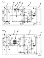
- Fig. 1 contains a conventional, considered within the scope of the present invention device a DC voltage generator 1, a DC-DC converter 2 and an inverter 3.
- the DC voltage generator 1 is z. B. from a photovoltaic or fuel cell system and has its two outputs 4 (+) and 5 (-) connected in parallel capacitor C (eg. US 2007 / 0047277A1 , Fig. 10).
- the inverter 3 of the known device has two outputs 6 and 7, which serve here for single-phase supply of electrical energy into a power supply network 8, whose phase L is connected to the output 6 and the neutral or neutral conductor N to the output 7.
- the inverter 3 also includes three inputs E1, E2 and E3. Between the inputs E1 and E2 two series-connected capacitors C1 and C2 are arranged, whose connection point is located at the input E3.
- the capacitors C1 and C2 form a conventional, bipolar voltage intermediate circuit of the inverter 3.
- the inverter 3 is according to Fig. 1 designed as a half-bridge inverter and provided with two switches S1 and S2, whose one.
- Connection is connected to one of the inputs E1 and E2 and their other connection to a common connection point 9 and from there via a smoothing or line reactor L1 to the output 6 leads.
- Both switches S1, S2 are also each a diode D1, D2 connected in parallel, the diode D1 from the connection point 9 in the direction of the input E1 and the diode D2 from the input E3 in the direction of the connection point 9 can be made conductive and in the opposite Direction locks.
- the input E3 is connected directly to the output 7, on the other hand connected to ground and thus formed as a ground terminal and connected to the negative output 5 of the DC voltage generator 1.
- the DC-DC converter 2 has two to be connected to the outputs 4 and 5 of the DC voltage generator 1 inputs 10 and 11.
- a switch S4 is connected to a connection point 14 leads.
- connection point 14 of the one terminal of a throttle designed as a coupled storage throttle 15 is connected.
- the storage inductor 15 includes a first winding W1 and a second winding W2, both magnetically coupled together and z. B. are wound on a common core 16. At one end, the two windings W1, W2 are connected together to form a further connection point.
- the input E3 of the inverter 3 designed as a ground connection is galvanically connected not only to the input 11 to be connected to the negative output 5 of the DC voltage generator 1, but also to the connection point of the two windings W1, W2 of the DC voltage converter 2.
- the other terminal of the winding W2 is connected via a diode D4 to the input E1 and the input E2 via a further diode D5 to the connection point 14 between the switch S4 and the winding W1.
- a first circuit, starting from the input 10 of the DC-DC converter 3, is formed by the switch S4, the winding W1 connected in series therewith and a power leading from the connection point of the two windings W1, W2 to the input 11.
- a second circuit contains the first winding W1 and leads back from the connection point 14 via the first winding W1, the ground terminal E3, a capacitor C2 associated with the winding W1, and the diode D5, all in series, to the connection point 14.
- a third circuit Finally, the second winding W2 and leads from the connection point of the two windings W1, W2 via the winding W2 and the diode D4 to the input E1, from there via the other of the two, the winding W2 associated capacitor C1 to the ground terminal E3 and from there back to the connection point between the two windings W1 and W2.
- the two windings W1, W2 are wound on the common core 16 such that the winding W2 is also charged when the winding W1 is charged due to the magnetic coupling through the first winding W1.
- the winding sense of both windings W1, W2 is chosen so that at in Fig. 1 indicated by points indicated points the same voltage polarities are obtained.
- the switches S1, S2 and S4 are expediently designed in a known manner as a semiconductor switch, which can be periodically switched on and off during operation with control units, not shown (microcontroller, PWM controllers, etc.), wherein the switching frequency z. B. 16 kHz or more.
- the switches S1, S2 are alternately turned on and off. This z. B. during the positive half cycle of the switching signal (switch S1 initially closed, switch S2 open) the positive side relative to E3 (input E1) of the capacitor C1 via the connection point 9 and the line choke L1 to the phase L. At the subsequent opening of the switch S1, the current can flow through the line reactor L1, the capacitor C2 and the diode D2.
- the negative side (input E2) of the capacitor C2 is connected to the phase L via the connection point 9 and the inductor L1 Close the switch S2 can continue to flow through the diode D1 and the capacitor C1.
- the two capacitors C1, C2 are thereby alternately discharged and recharged.
- the described design of the DC-DC converter 2 has the advantage that the DC voltage generator 1 can be operated with a comparatively large range of output voltages. If the DC-DC converter 2 were missing, then it would have to be ensured that the DC voltage generator 1 always supplies such a high output voltage to the inputs E1 and E2 even under unfavorable conditions that the capacitors C1 and C2 are charged to a higher voltage than the network amplitude (in FIG usually approx. ⁇ 325 V).
- the voltages across the capacitors C1, C2 can also be set to the desired level via the choice of the duty cycle with which the switch S4 is operated if the output voltage of the DC voltage generator 1 is smaller, at least as required by the inverter 3 (or the grid 8).
- the extent known device is still very flexible. This results from the fact that the voltages at C1 and C2 depending on the chosen duty cycle for S4 can be both larger and smaller than the input voltage to the capacitor C. If the duty ratio is greater than 0.5, then the DC-DC converter works higher setting. If the duty cycle is less than 0.5, then the DC-DC converter 2 works in depth. A duty cycle of 0.5 leads practically to a direct feed of the voltage applied to the output of the DC voltage generator 1 voltage. Thus, a large operating voltage range is obtained with only one switch in the DC-DC converter 2 in a grounded DC voltage generator 1.
- the maximum voltage load of the inverter switches S1 and S2 is about 2 * UC1, where UC1 is the maximum voltage across the capacitor C1. In the simplest case, only one of these switches can be switched to high frequency for half the grid period, while the other remains off. In addition, a continuous current flow in the network 8 is possible on the inverter side.
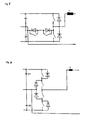
- Fig. 2 shows a first embodiment of the device according to the invention, in which the desired effects by means of a coupled storage throttle 15 accordingly Fig. 1 as well as with two switches S5, S6 and three diodes D6, D7 and D8 can be achieved, ie also here the circuit complexity is low.
- a first switch S5 is connected between the input 10 and a connection point 22, to which one terminal of the winding W1 of the storage inductor 15 is connected.
- the other terminal of the winding W1 is connected via a second connection point 23 and by means of a second switch S6 to the input E3 of the inverter 3 designed as ground terminal, which is also connected to the input 11 of the DC-DC converter 2 or to the negative output 5 of the DC voltage generator 1 is used.
- the current path of 10 across S5, 22, W1, 23, S6, 11 and back to 10 forms a first circuit.
- Fig. 2 a starting from the ground terminal E3 first diode D6 via the connection point 22, the winding W1, the connection point 23, a second diode D7 and the winding W1 here associated capacitor C1 back to the ground terminal E3.
- a third circuit containing the second winding W2 which leads back from the earth terminal E3 via the capacitor C2 assigned here to the winding W2, a third diode D8 and the second winding W2 back to the earth terminal E3.
- the device is after Fig. 2 as flexible as the device according to Fig. 1 because the voltages at C1 and C2 can be both larger and smaller than the output voltage at the DC voltage generator 1, so that a high operating voltage range is achieved.
- the arrangement in this case is such that a center terminal or a winding tap 21 of the winding W1 is connected to a connection point 22 to the first switch S5 and the part W11 of the winding W1 fixed by this tap 21 is in the first circuit which is charging the storage inductor 20 is used, whereas the second circuit contains the entire, lying between the diodes D6 and D7 first winding W1 and the part W11 + W12 thereof.
- the tap 21 according to Fig. 5 be placed at a connection point 24 to the second switch S6, while from the parts W11 and W12 formed part of the storage throttle 15 as in Fig. 2 is placed between the connection points 22 and 23.
- Fig. 6 shows an embodiment, by dividing the first winding W1 of a storage choke 25 even when using only one switch S4 having device after Fig. 1 a reduction of the voltage load allows.
- the tap 26 is connected to the switch S4, whereas the normal input terminal of W1 as in Fig. 1 is connected to the output of the diode D5.
- the portion W11 of the first winding W1 between the tap 26 and an output terminal is in the above-described first electric circuit (10, S4, 14, W11, 11), while as shown in FIG Fig.
- the entire winding W1 or a part W11 + W12 thereof is in the second circuit with C2 and D5.
- the location of the tap 26 may be as in Fig. 4 and 5 be chosen arbitrarily in principle.
- the operation of the inverter 3 is substantially identical in all cases described above.
- Fig. 7 shows a half-bridge inverter in 3-point circuit
- Fig. 8 another inverter in 3-point circuit with center (in each case in 1-phase design)
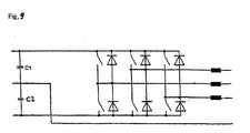
- Fig. 9 an inverter for 3-phase supply to the grid 8. All three inverters have a bipolar voltage link, the inputs E1 to E3 and the outputs 6, 7 as described above. Since inverters of this type are known per se, further explanations do not appear to be necessary.
- the magnetic coupling of the windings W1 and W2 is preferably obtained by winding them on top of each other or successively onto a common core as needed. They preferably have the same number of turns and become in the schematically illustrated arrangement Fig. 2 and 4 suitably wound with opposite winding sense on the core 16 in order to obtain the correct current directions in the loading and unloading operations.
- the invention is not limited to the described embodiments, which can be modified in many ways. This applies in particular to the extent that the inverters 3 and the DC-DC converters 2 can be manufactured and sold as separate components, although they are preferably produced and sold as a finished unit, as can be seen from the drawings. Therefore, the invention relates not only to the combination of a DC-DC converter 2 and an inverter 3, but also the DC-DC converter 2 alone. Furthermore, it is clear that in the above description, only the necessary components for understanding the invention have been described and in particular the necessary and known control organs, MPP regulations, etc. may be additionally present. It will also be understood that the various features may be applied in combinations other than those described and illustrated.
Abstract
Description
Die Erfindung betrifft eine Vorrichtung der im Oberbegriff des Anspruchs 1 angegebenen Gattung und einen dafür geeigneten Gleichspannungswandler.The invention relates to a device of the type specified in the preamble of
Zur Einspeisung elektrischer Energie, die mit Gleichspannungsgeneratoren wie z. B. Photovoltaik- oder Brennstoffzellenanlagen erzeugt wird, in ein Wechselstromnetz, insbesondere das öffentliche Energieversorgungsnetz (50/60 Hz), werden Wechselrichter der verschiedensten Art verwendet. Zwischen dem Gleichspannungsgenerator und dem Wechselrichter ist in den meisten Fällen ein Gleichspannungswandler (DC-DC-Steller) vorgesehen, der dem Zweck dient, die vom Gleichspannungsgenerator gelieferte Gleichspannung in eine vom Wechselrichter benötigte bzw. an diesen angepasste Gleichspannung umzuwandeln.For feeding electrical energy with DC generators such. B. photovoltaic or fuel cell systems is generated, in an AC network, in particular the public power grid (50/60 Hz), inverters of various kinds are used. Between the DC voltage generator and the inverter, a DC-DC converter is provided in most cases, which serves the purpose of converting the DC voltage supplied by the DC voltage generator into a required by the inverter or adapted to this DC voltage.
Aus verschiedenen Gründen ist es erwünscht, einen der Ausgänge des Gleichspannungsgenerators zu erden, wobei im Rahmen der vorliegenden Erfindung insbesondere solche Fälle betrachtet werden, bei denen der Erdanschluss am negativen Ausgang des Gleichspannungsgenerators vorgesehen wird. Der Grund für die gewünschte Erdung besteht einerseits darin, dass es Länder gibt, in denen eine solche Erdung vorgeschrieben ist. Andererseits ergeben sich bei fehlender Erdung verschiedene Nachteile beim Betrieb. Hierzu zählt u. a. das Problem der hochfrequenten Ableitströme. Aufgrund von unvermeidbaren parasitären Kapazitäten zwischen dem Gleichspannungsgenerator und Erde kann es bei Potentialschwankungen zu nicht unerheblichen Ausgleichsströmen kommen, die ein nicht tolerierbares Sicherheitsrisiko darstellen, daher zum Berührungsschutz bzw. zur Herstellung der elektromagnetischen Verträglichkeit (EMV) aufwendige Überwachungsmaßnahmen mit Hilfe von Fehlerstromsensoren od. dgl. erforderlich machen und nur durch Erdung sicher vermieden können. Potentialschwankungen am Gleichspannungsgenerator können weiter bei bestimmten Solarmodulen wie z. B. Dünnschichtmodulen od. dgl. zu dauerhaften Zerstörungen führen.For various reasons, it is desirable to ground one of the outputs of the DC voltage generator, in the context of the present invention in particular those cases are considered in which the ground terminal is provided at the negative output of the DC voltage generator. The reason for the desired grounding is, on the one hand, that there are countries in which such a grounding is prescribed. On the other hand, there are various disadvantages in the operation in the absence of grounding. These include the problem of high-frequency leakage currents. Due to unavoidable parasitic capacitances between the DC voltage generator and earth can be at potential fluctuations to significant compensation currents that represent an intolerable security risk, therefore od contact protection or for the production of electromagnetic compatibility (EMC) complex monitoring measures using fault current sensors od. Like. Required and safe only by grounding can be avoided. Potential fluctuations in the DC voltage generator can continue with certain solar modules such. B. thin-film modules od. Like. Lead to permanent destruction.
Eine Erdung der beschriebenen Art ist ohne weiteres dann möglich, wenn Gleichspannungswandler mit Transformatoren verwendet werden, die eine galvanische Trennung der Gleichspannungsseite von der Wechselspannungsseite herbeiführen. Transformatoren haben aber unabhängig davon, ob Netztransformatoren oder Hochfrequenztransformatoren verwendet werden, u. a. eine Reduzierung des Wirkungsgrades, zum Teil erhebliche Gewichte und Baugrößen und/oder einen zusätzlichen Regelungsaufwand zur Folge, weshalb grundsätzlich transformatorlose Spannungswandler bevorzugt werden. Die üblichen Topologien von transformatorlosen Gleichspannungswandlern machen jedoch die gewünschte Erdung entweder unmöglich, da dies zum Kurzschließen von benötigten Schaltern, Kapazitäten od. dgl. führen würde, oder haben einen erhöhten Schaltungsaufwand und andere Nachteile zur Folge.A grounding of the type described is readily possible when DC-DC converters are used with transformers, which cause a galvanic separation of the DC side from the AC side. However, transformers, regardless of whether mains transformers or high-frequency transformers are used, u. a. a reduction of the efficiency, sometimes considerable weights and sizes and / or an additional control effort result, which is why transformerless voltage transformers are preferred. The usual topologies of transformerless DC-DC converters, however, either make the desired grounding impossible, as this would result in the short circuiting of required switches, capacitors, or the like, or result in increased circuit complexity and other disadvantages.
Es sind daher bereits zahlreiche Versuche unternommen worden, das Auftreten der genannten Nachteile auf anderem Wege zu vermeiden. Insbesondere sind Schaltungen bekannt, die dem Zweck dienen, die unerwünschten Ableitströme zu reduzieren (z. B.
Weiterhin ist eine Schaltungsanordnung bekannt (
Daneben sind auch bereits Schaltungsanordnungen bekannt, mit denen ein Solargenerator trotz Fehlens eines Transformators einseitig geerdet werden kann. Dadurch werden kapazitive Ableitströme prinzipbedingt verhindert. Eine dieser Schaltungsanordnungen (
Schließlich sind Vorrichtungen der eingangs bezeichneten Gattung bekannt (
Der Gleichspannungswandler dieser bekannten Vorrichtung enthält eine Speicherdrossel, zwei Dioden und einen Schalter. Der Erdanschluss des Wechselrichters kann in diesem Fall mit dem negativen Ausgang des Gleichspannungsgenerators verbunden werden. Dies wird durch Anwendung einer Speicherdrossel ermöglicht, die aus zwei magnetisch gekoppelten Wicklungen zusammengesetzt ist. Die beiden Wicklungen dieser Speicherdrossel sind an einem Ende derart galvanisch miteinander verbunden, dass einerseits bei geschlossenem Schalter eine der beiden Wicklungen vom Gleichspannungsgenerator und die andere Wicklung aufgrund der magnetischen Kopplung über die erste Wicklung aufgeladen wird und dass andererseits bei offenem Schalter beide Wicklungen über je einen zugeordneten der beiden Kondensatoren und eine zugehörige Diode entladen werden.The DC-DC converter of this known device includes a storage inductor, two diodes and a switch. The ground connection of the inverter can in this case be connected to the negative output of the DC voltage generator. This is made possible by using a storage choke, which is composed of two magnetically coupled windings. The two windings of this storage inductor are so galvanically connected at one end, that on the one hand with the switch closed one of the two windings of the DC voltage generator and the other winding is charged due to the magnetic coupling on the first winding and that on the other hand with an open switch both windings are discharged via an associated one of the two capacitors and an associated diode.
Dem Vorteil, dass diese Vorrichtung mit vergleichsweise einfachen Mitteln, insbesondere ohne Transformator und mit nur einem Schalter eine Erdung des Gleichspannungsgenerators ermöglicht, steht der Nachteil gegenüber, dass der Schalter im geöffneten Zustand mit einer Spannung belastet wird, die sich aus der Summe der Ausgangsspannung des Gleichspannungsgenerators und der Spannung an einem der beiden Kondensatoren des Spannungszwischenkreises des Wechselrichters ergibt. Daraus folgt umgekehrt, dass die Ausgangsspannung des Gleichspannungsgenerators höchstens gleich der Differenz aus der zulässigen Spannung am Schalter und der Spannung am betreffenden Kondensator sein darf, um eine Zerstörung des Schalters mit Sicherheit zu vermeiden. Derartige Begrenzungen für die Ausgangsspannung des Gleichspannungsgenerators sind unerwünscht. Um die fließenden Ströme und damit die Verluste klein zuhalten, sind vielmehr Spannungen erwünscht, die wesentlich größer sind, als der genannten Spannungsdifferenz entspricht, so dass entweder aufwendige, entsprechend hoch belastbare Schalter erforderlich sind oder, bei Anwendung üblicher Schalter, eine Reduzierung der Ausgangsspannung am Gleichspannungsgenerator unerlässlich ist. Vorrichtungen dieser Art haben daher einen eingeschränkten Anwendungsbereich.The advantage that this device with comparatively simple means, in particular without a transformer and with only one switch allows grounding of the DC voltage generator, is the disadvantage that the switch is loaded in the open state with a voltage resulting from the sum of the output voltage of DC voltage generator and the voltage at one of the two capacitors of the voltage intermediate circuit of the inverter results. Conversely, it follows that the output voltage of the DC generator may at most equal to the difference between the allowable voltage at the switch and the voltage across the capacitor in question to avoid destruction of the switch with certainty. Such limitations for the output voltage of the DC voltage generator are undesirable. In order to keep the flowing currents and thus the losses small, rather voltages are desired which are substantially greater than the said voltage difference corresponds, so that either expensive, correspondingly high load switch are required or, when using conventional switches, a reduction of the output voltage on DC generator is essential. Devices of this type therefore have a limited scope.
Aus der
Ausgehend von diesem Stand der Technik besteht das technische Problem der Erfindung darin, die Vorrichtung der eingangs bezeichneten Gattung und insbesondere einen dafür geeigneten Gleichspannungswandler so auszubilden, dass eine Erdung des negativen Anschlusses des Gleichspannungsgenerators nicht nur ebenfalls mit vergleichsweise einfachen konstruktiven Mitteln, sondern auch unter deutlicher Reduzierung der Spannungsbelastung des Schalters des Gleichspannungswandlers realisiert werden kann.Based on this prior art, the technical problem of the invention is the device of the type described and in particular a suitable DC-DC converter so that a grounding of the negative terminal of the DC generator not only with comparatively simple design means, but can be realized with significant reduction of the voltage load of the switch of the DC-DC converter.
Gelöst wird dieses Problem erfindungsgemäß mit den kennzeichnenden Merkmalen der Ansprüche 1, 2 und 11.This problem is solved according to the invention with the characterizing features of
Die Erfindung ermöglicht einen geerdeten Betrieb des Gleichspannungs-generators durch Anwendung eines Gleichspannungswandlers, der im einfachsten Fall lediglich eine Speicherdrossel, drei Dioden und zwei Schalter benötigt. Dadurch wird trotz eines nur geringfügig erhöhten Aufwands der Vorteil erzielt, dass die maximale Belastung eines der Schalter nicht größer ist, als der Ausgangsspannung des Gleichspannungsgenerators entspricht, während die Spannungsbelastung am anderen Schalter nicht größer als die Spannung eines der Kondensatoren ist, so dass die Ausgangsspannung des Gleichspannungsgenerators im Gegensatz zur gattungsgemäßen Vorrichtung bis zur Belastungsgrenze der Schalter erhöht werden kann.The invention enables a grounded operation of the DC voltage generator by using a DC-DC converter, which requires in the simplest case, only one storage inductor, three diodes and two switches. Thereby, despite only a slightly increased cost, the advantage that the maximum load of one of the switches is not greater than the output voltage of the DC voltage generator corresponds, while the voltage load on the other switch is not greater than the voltage of one of the capacitors, so that the output voltage the DC voltage generator in contrast to the generic device can be increased up to the load limit of the switch.
Weitere vorteilhafte Merkmale der Erfindung ergeben sich aus den Unteransprüchen.Further advantageous features of the invention will become apparent from the dependent claims.
Die Erfindung wird nachfolgend in Verbindung mit den beiliegenden Zeichnungen an Ausführungsbeispielen näher erläutert. Es zeigen:
-
Fig. 1 den bekannten Aufbau einer Vorrichtung mit einem geerdeten Gleichspannungsgenerator zur Einspeisung elektrischer Energie in ein Energieversorgungsnetz; -
Fig. 2 eine erfindungsgemäße Vorrichtung, mit einem geerdeten Gleichspannungsgenerator zur Einspeisung elektrischer Energie in ein Energieversorgungsnetz; -
Fig. 3 die Signale zur Steuerung von zwei Schaltern der Vorrichtung nachFig. 2 und daraus resultierende Stromverläufe; -
Fig. 4 und5 eine Vorrichtung entsprechendFig. 2 , jedoch mit einem jeweils modifizierten Gleichspannungswandler; -
Fig. 6 eine Vorrichtung entsprechendFig. 1 , jedoch mit einem modifizierten Gleichspannungswandler; und -
Fig. 7 bis 9 verschiedene Typen von Wechselrichtern, die alternativ zum Wechselrichter nachFig. 1 mit dem erfindungsgemäßen Gleichspannungswandler betrieben werden können.
-
Fig. 1 the known structure of a device with a grounded DC generator for feeding electrical energy into a power grid; -
Fig. 2 a device according to the invention, with a grounded DC voltage generator for feeding electrical energy into a power supply network; -
Fig. 3 the signals for controlling two switches of the device according toFig. 2 and resulting current waveforms; -
Fig. 4 and5 a device accordinglyFig. 2 but with a respective modified DC-DC converter; -
Fig. 6 a device accordinglyFig. 1 but with a modified DC-DC converter; and -
Fig. 7 to 9 different types of inverters, the alternative to the inverter afterFig. 1 can be operated with the DC-DC converter according to the invention.
Nach
Der Wechselrichter 3 der bekannten Vorrichtung weist zwei Ausgänge 6 und 7 auf, die hier zur einphasigen Einspeisung elektrischer Energie in ein Energieversorgungsnetz 8 dienen, dessen Phase L mit dem Ausgang 6 und dessen Null- oder Neutralleiter N mit dem Ausgang 7 verbunden wird. Der Wechselrichter 3 enthält außerdem drei Eingänge E1, E2 und E3. Zwischen den Eingängen E1 und E2 sind zwei in Serie verbundene Kondensatoren C1 und C2 angeordnet, deren Verbindungspunkt am Eingang E3 liegt. Die Kondensatoren C1 und C2 bilden einen üblichen, bipolaren Spannungszwischenkreis des Wechselrichters 3. Der Wechselrichter 3 ist gemäß
Der Gleichspannungswandler 2 hat zwei mit den Ausgängen 4 und 5 des Gleichspannungsgenerators 1 zu verbindende Eingänge 10 und 11. An den Eingang 10 ist ein Schalter S4 angeschlossen, der zu einem Verbindungspunkt 14 führt. An diesem Verbindungspunkt 14 ist der eine Anschluss einer als gekoppelte Drossel ausgebildeten Speicherdrossel 15 angeschlossen. Die Speicherdrossel 15 enthält eine erste Wicklung W1 und eine zweiten Wicklung W2, die beide magnetisch miteinander gekoppelt und dazu z. B. auf einen gemeinsamen Kern 16 gewickelt sind. An ihren einen Enden sind die beiden Wicklungen W1, W2 unter Bildung eines weiteren Verbindungspunktes miteinander verbunden.The DC-
Der als Erdanschluss ausgebildete Eingang E3 des Wechselrichters 3 ist nicht nur mit dem an den negativen Ausgang 5 des Gleichspannungsgenerators 1 anzuschließenden Eingang 11, sondern auch mit dem Verbindungspunkt der beiden Wicklungen W1, W2 des Gleichspannungswandlers 2 galvanisch verbunden. Außerdem ist der andere Anschluss der Wicklung W2 über eine Diode D4 mit dem Eingang E1 und der Eingang E2 über eine weitere Diode D5 mit dem Verbindungspunkt 14 zwischen dem Schalter S4 und der Wicklung W1 verbunden. Dadurch sind insgesamt drei Stromkreise entstanden. Ein erster Stromkreis wird, ausgehend vom Eingang 10 des Gleichspannungswandlers 3, vom Schalter S4, der damit in Serie liegenden Wicklung W1 und einer vom Verbindungspunkt der beiden Wicklungen W1, W2 zum Eingang 11 führenden Leistung gebildet. Ein zweiter Stromkreis enthält die erste Wicklung W1 und führt vom Verbindungspunkt 14 über die erste Wicklung W1, den Erdanschluss E3, einen der Wicklung W1 zugeordneten Kondensator C2 und die Diode D5, die sämtlich in Serie liegen, zurück zum Verbindungspunkt 14. Ein dritter Stromkreis enthält schließlich die zweite Wicklung W2 und führt vom Verbindungspunkt der beiden Wicklungen W1, W2 über die Wicklung W2 und die Diode D4 zum Eingang E1, von dort über den anderen der beiden, der Wicklung W2 zugeordneten Kondensator C1 zum Erdanschluss E3 und von dort zurück zum Verbindungspunkt zwischen den beiden Wicklungen W1 und W2.The input E3 of the
Die beiden Wicklungen W1, W2 sind so auf den gemeinsamen Kern 16 gewickelt, dass die Wicklung W2 beim Laden der Wicklung W1 aufgrund der magnetischen Kopplung durch die erste Wicklung W1 ebenfalls aufgeladen wird. Der Wicklungssinn beider Wicklungen W1, W2 ist dabei so gewählt, dass an in
Die Schalter S1, S2 und S4 sind in bekannter Weise zweckmäßig als Halbleiterschalter ausgebildet, die beim Betrieb mit nicht dargestellten Steuereinheiten (Microcontroller, PWM-Steuerungen usw.) periodisch ein- und ausgeschaltet werden können, wobei die Schaltfrequenz z. B. 16 kHz oder mehr beträgt.The switches S1, S2 and S4 are expediently designed in a known manner as a semiconductor switch, which can be periodically switched on and off during operation with control units, not shown (microcontroller, PWM controllers, etc.), wherein the switching frequency z. B. 16 kHz or more.
Die Arbeitsweise der beschriebenen Vorrichtung ist im Wesentlichen wie folgt:
- Auf der Seite des
Gleichspannungsgenerators 1 wird bei geschlossenem Schalter S4die gekoppelte Speicherdrossel 15 mit Hilfe des ersten Stromkreises 10, S4, W1, 11 geladen. Bei geöffnetem Schalter S4 kann sich die Wicklung W1 über den zweiten Stromkreis mit C2 entladen (über den Pfad 14, W1, E3, C2, E2, D5 und 14), während sich die Wicklung W2 über den dritten Stromkreis mit C1 entladen kann über dem Ptad vom Verbindungspunkt den beiden Wicklungen W1, W2 über W2, D4, E1, C1, E3 zum Verbindungspunkt den Wicklungen W1, W2. Für diese Funktionen werden nur ein Schalter (S4), eine gekoppelte Speicherdrossel (15) und zwei Dioden (D4, D5) benötigt, so dass der Aufwand vergleichsweise gering und der Wirkungsgrad groß ist. Außerdem ist, wie gewünscht, dernegative Ausgang 5 desGleichspannungsgenerators 1 geerdet bzw. an Erde anschließbar, wie dies auch für den Neutralleiter N des Netzes 8 gilt. Der Spannungszwischenkreis hat hier somit drei wirksame Anschlüsse E1, E2 und E3, andie der Gleichspannungswandler 2mit Ausgängen dem Eingang 11 angeschlossen ist bzw. angeschlossen werden kann, wenn er als separates Schaltungsteil hergestellt und/oder angeboten wird.
- On the side of the
DC voltage generator 1, when the switch S4 is closed, the coupledstorage inductor 15 is charged by means of the firstelectric circuit 10, S4, W1, 11. With switch S4 open, winding W1 can discharge via C2 via the second circuit (viapath 14, W1, E3, C2, E2, D5 and 14), while winding W2 can discharge across C1 via the third circuit Ptad from the connection point the two windings W1, W2 via W2, D4, E1, C1, E3 to the connection point the windings W1, W2. For these functions, only one switch (S4), a coupled storage inductor (15) and two diodes (D4, D5) are required, so that the effort is comparatively low and the efficiency is high. In addition, as desired, thenegative output 5 of theDC voltage generator 1 is grounded or connectable to ground, as is true for the neutral conductor N of thenetwork 8. The voltage intermediate circuit thus has three effective terminals E1, E2 and E3, to which the DC-DC converter 2 withoutputs input 11 is connected or can be connected when it is manufactured as a separate circuit part and / or offered.
Auf der Seite des Wechselrichters 3 werden die Schalter S1, S2 abwechselnd ein- bzw. ausgeschaltet. Dadurch wird z. B. während der positiven Halbwelle des Schaltsignals (Schalter S1 zunächst geschlossen, Schalter S2 offen) die gegenüber E3 positive Seite (Eingang E1) des Kondensators C1 über den Verbindungspunkt 9 und die Netzdrossel L1 an die Phase L gelegt. Beim nachfolgenden Öffnen des Schalters S1 kann der Strom weiter durch die Netzdrossel L1, den Kondensator C2 und die Diode D2 fließen. Während der negativen Halbwelle des Netzes 8 (Schalter S1 offen, Schalter S2 zunächst geschlossen) wird dagegen die gegenüber E3 negative Seite (Eingang E2) des Kondensators C2 über den Verbindungspunkt 9 und die Drossel L1 an die Phase L gelegt, wobei der Strom nach dem Schließen des Schalters S2 weiter durch die Diode D1 und den Kondensator C1 fließen kann. Die beiden Kondensatoren C1, C2 werden dadurch abwechselnd entladen und wieder geladen.On the side of the
Bei symmetrischer Belastung und gleicher Windungszahl von W1 und W2 sind die Spannungen an C1 und C2 gleich groß. Wird beim Betrieb z. B. C1 stärker vom netzseitigen Wechselrichter 3 als C2 belastet, so wird automatisch der Ladestrom aus W2 größer als der aus W1. Die Schaltung "symmetriert" sich dadurch selbsttätig, was eine Grundvoraussetzung für den Betrieb des Wechselrichters 3 auf der Netzseite ist.With symmetrical load and same number of turns of W1 and W2, the voltages at C1 and C2 are the same. Is the operation z. B. C1 loaded more heavily from the grid-
Die beschriebene Ausbildung des Gleichspannungswandlers 2 bringt den Vorteil mit sich, dass der Gleichspannungsgenerator 1 mit einem vergleichsweise großen Bereich von Ausgangsspannungen betrieben werden kann. Würde der Gleichspannungswandler 2 fehlen, dann müsste sichergestellt werden, dass der Gleichspannungsgenerator 1 auch unter ungünstigen Verhältnissen stets eine so hohe Ausgangsspannung an die Eingänge E1 und E2 liefert, dass die Kondensatoren C1 und C2 auf eine höhere Spannung aufgeladen werden, als der Netzamplitude (in der Regel ca. ± 325 V) entspricht. Ist dagegen ein hochsetzender Gleichspannungswandler 2 vorhanden, dann können die Spannungen an den Kondensatoren C1, C2 über die Wahl des Tastverhältnisses, mit dem der Schalter S4 betrieben wird, auch dann auf die gewünschte Höhe eingestellt werden, wenn die Ausgangsspannung des Gleichspannungsgenerators 1 kleiner ist, als vom Wechselrichter 3 (bzw. vom Netz 8) mindestens benötigt wird.The described design of the DC-
Die insoweit bekannte Vorrichtung ist weiterhin sehr flexibel einsetzbar. Das ergibt sich daraus, dass die Spannungen an C1 und C2 in Abhängigkeit vom gewählten Tastverhältnis für S4 sowohl größer als auch kleiner als die Eingangsspannung am Kondensator C sein können. Ist das Tastverhältnis größer als 0,5, dann arbeitet der Gleichspannungswandler hochsetzend. Ist das Tastverhältnis kleiner als 0,5, dann arbeitet der Gleichspannungswandler 2 tiefsetzend. Ein Tastverhältnis von 0,5 führt praktisch zu einer Direkteinspeisung der am Ausgang des Gleichspannungsgenerators 1 anliegenden Spannung. Damit wird ein großer Betriebsspannungsbereich mit nur einem Schalter im Gleichspannungswandler 2 bei einem geerdeten Gleichspannungsgenerator 1 erhalten. Die maximale Spannungsbelastung der Wechselrichterschalter S1 und S2 beträgt etwa 2 · UC1, wobei UC1 die maximale Spannung am Kondensator C1 ist. Im einfachsten Fall kann auch immer nur einer dieser Schalter pro halber Netzperiode hochfrequent geschaltet werden, während der andere ausgeschaltet bleibt. Außerdem ist auf der Wechselrichterseite ein kontinuierlicher Stromfluss in das Netz 8 möglich.The extent known device is still very flexible. This results from the fact that the voltages at C1 and C2 depending on the chosen duty cycle for S4 can be both larger and smaller than the input voltage to the capacitor C. If the duty ratio is greater than 0.5, then the DC-DC converter works higher setting. If the duty cycle is less than 0.5, then the DC-
Ein Nachteil der beschriebenen Vorrichtung besteht, wie bereits oben näher erläutert wurde, in der Belastung des Schalters S4 im offenen Zustand mit einer Spannung US4 = UC + UC2, wobei UC und UC2 die Spannungen an den Kondensatoren C und C2 sind. Dieser Nachteil wird erfindungsgemäß vermieden.A disadvantage of the device described is, as already explained above, in the load of the switch S4 in the open state with a voltage US4 = UC + UC2, where UC and UC2 are the voltages at the capacitors C and C2. This disadvantage is avoided according to the invention.
Weiterhin ist gemäß
Die Signale für die Ansteuerung der Schalter S5 und S6 sowie die Stromverläufe in den Wicklungen W1, W2 der Speicherdrossel 15 ergeben sich beispielhaft aus
Beim gleichzeitigen Einschalten der Schalter S5 und S6 wird der beschriebene erste Stromkreis geschlossen, wodurch die Speicherdrossel 15 in der oben beschriebenen Weise geladen wird. Befinden sich die Schalter S5, S6 dagegen im geöffneten Zustand, dann wird einerseits die Wicklung W1 über D6, W1, D7 und C1 und andererseits die Wicklung W2 über C2 und D8 entladen. Wie in
Mit der Vorrichtung nach
Im übrigen ist die Vorrichtung nach
Alternativ kann die Anzapfung 21 gemäß
Die Arbeitsweise des Wechselrichters 3 ist in allen oben beschriebenen Fällen im Wesentlichen identisch.The operation of the
Obwohl die bisherige Beschreibung ausschließlich auf den als Halbbrückenwechselrichter ausgebildeten Wechselrichter 3 Bezug nimmt, ist für den Fachmann klar, dass auch andere Wechselrichter mit einem bipolaren Spannungszwischenkreis an den erfindungsgemäßen Gleichspannungswandler 2 angeschlossen werden können. Das ist schematisch in
Die magnetische Kopplung der Wicklungen W1 und W2 wird vorzugsweise dadurch erhalten, dass sie je nach Bedarf übereinander oder hintereinander auf einen gemeinsamen Kern gewickelt werden. Sie weisen vorzugsweise dieselben Windungszahlen auf und werden bei der schematisch dargestellten Anordnung nach
Die Erfindung ist nicht auf die beschriebenen Ausführungsbeispiele beschränkt, die auf vielfache Weise abgewandelt werden können. Das gilt insbesondere auch insoweit, als die Wechselrichter 3 und die Gleichspannungswandler 2 als voneinander getrennte Bauteile hergestellt und vertrieben werden können, wenn sie auch bevorzugt, wie aus den Zeichnungen ersichtlich ist, als eine fertige Baueinheit hergestellt und vertrieben werden. Daher betrifft die Erfindung nicht nur die Kombination aus einem Gleichspannungswandler 2 und einem Wechselrichter 3, sondern auch den Gleichspannungswandler 2 allein. Weiterhin ist klar, dass in der obigen Beschreibung nur die zum Verständnis der Erfindung erforderlichen Bauteile beschrieben wurden und insbesondere die erforderlichen und an sich bekannten Steuerorgane, MPP-Regelungen usw. zusätzlich vorhanden sein können. Außerdem versteht sich, dass die verschiedenen Merkmale auch in anderen als den beschriebenen und dargestellten Kombinationen angewendet werden können.The invention is not limited to the described embodiments, which can be modified in many ways. This applies in particular to the extent that the
Claims (11)
- Device for feeding electrical energy into a power grid (8), including a direct voltage converter (2), which is intended for connection to a direct voltage generator (1), and an inverter (3), which is connected thereto and intended for connection to the power grid (8) and which comprises a bipolar voltage intermediate circuit with two capacitors (C1, C2), which are arranged in series and which are connected together at an earth connection (E3) that is connected to a negative output (5) of the direct voltage generator (1), wherein the direct voltage converter (2) comprises at least two diodes, a switch and a storage choke, which comprises a first winding (W1) and a second winding (W2), wherein these two windings (W1, W2) are magnetically coupled together and electrically connected together by a respective one of their terminals in such a manner that in a first switching state the first winding (W1) is charged by the direct voltage generator (1) and the second winding (W2) is charged via the first winding (W1) due to the magnetic coupling and in a second switching state the two windings (W1, W2) are respectively discharged via an associated one of the two capacitors (C1, C2) and an associated diode, characterised in that a first terminal of the first winding (W1) is connected at a first connecting point (22) to a first switch (S5) and a second terminal of the first winding (W1) is connected at a second connecting point (23) to a second switch (S6) such that the first winding (W1) on the one hand provides, together with the two switches (S5, S6), a first electric circuit that is connected to associated outputs (4, 5) of the direct voltage generator (1) and on the other hand is located in a second electric circuit that leads from the earth connection (E3) via a first diode (D6), the first connecting point (22), the first winding (W1), the second connecting point (23), a second diode (D7) and the capacitor (C1) associated therewith back to the earth connection (E3) and that the second winding (W2) is located in a third electric circuit that leads from the earth connection (E3) via the capacitor (C2) associated therewith, a third diode (D8) and the second winding (W2) back to the earth connection (E3).
- Device for feeding electrical energy into a power grid (8), including a direct voltage converter (2), which is intended for connection to a direct voltage generator (1), and an inverter (3), which is connected thereto and intended for connection to the power grid (8) and which comprises a bipolar voltage intermediate circuit with two capacitors (C1, C2), which are arranged in series and which are connected together at an earth connection (E3) that is connected to a negative output (5) of the direct voltage generator (1), wherein the direct voltage converter (2) comprises at least two diodes, a switch (S4) and a storage choke (25), which comprises a first winding (W1) and a second winding (W2), wherein these two windings (W1, W2) are magnetically coupled together and electrically connected together by a respective one of their terminals in such a manner that in a first switching state the first winding (W1) is charged by the direct voltage generator (1) and the second winding (W2) is charged via the first winding (W1) due to the magnetic coupling and in a second switching state the two windings (W1, W2) are respectively discharged via an associated one of the two capacitors (C1, C2) and an associated diode, characterised in that one of the windings (W1) is divided and provided with a winding tap (26) that is connected to the switch (S4) such that only a first part (W11) of the first winding (W1), which is determined by this tap (26), lies in a first electric circuit of three electric circuits, while a second part (W11 + W12) of the first winding (W1) is located in a second electric circuit of the three electric circuits, wherein the two windings (W1, W2) are wound on a common core.
- Device according to claim 1, characterised in that one of the windings (W1) is divided and provided with a winding tap (22) that is connected to one of the connecting points (21, 23) such that only a first part (W11) of the first winding (W1), which is determined by this tap (22), lies in the first electric circuit, whilst a second part (W11 + W12) of the first winding (W1) is located in the second electric circuit.
- Device according to claim 1, characterised in that the two windings (W1, W2) are wound on a common core (16).
- Device according to claim 4, characterised in that the windings (W1, W2) are wound on the core (16) in opposite winding senses.
- Device according to any one of claims 1 to 5, characterised in that the two windings (W1, W2) have the same number of winding turns.
- Device according to any one of claims 1 to 6, characterised in that the inverter (3) is configured to be an inverter having a half bridge.
- Device according to any one of claims 1 to 6, characterised in that the inverter (3) is configured to be an inverter with a half bridge in a three-point circuit (Fig. 7).
- Device according to any one of claims 1 to 6, characterised in that the inverter (3) is configured to be an inverter with a half bridge in a three-point circuit with a centre point (Fig. 8).
- Device according to any one of claims 1 to 6, characterised in that the inverter (3) is configured for a single-phase or three-phase feeding of the electrical energy to the power grid (8) (Figs. 2 to 8 or Fig. 9).
- Device according to claim 10, characterised in that the direct voltage converter (2) is combined with the inverter (3) to form a constructional unit.
Applications Claiming Priority (2)
| Application Number | Priority Date | Filing Date | Title |
|---|---|---|---|
| DE102007028077A DE102007028077B4 (en) | 2007-06-15 | 2007-06-15 | Device for feeding electrical energy into a power supply network and DC-DC converter for such a device |
| PCT/DE2008/000619 WO2008151587A1 (en) | 2007-06-15 | 2008-04-12 | Device for feeding electric energy into a power grid and dc converter for such a device |
Publications (2)
| Publication Number | Publication Date |
|---|---|
| EP2027647A1 EP2027647A1 (en) | 2009-02-25 |
| EP2027647B1 true EP2027647B1 (en) | 2011-09-28 |
Family
ID=39764741
Family Applications (1)
| Application Number | Title | Priority Date | Filing Date |
|---|---|---|---|
| EP08757930A Not-in-force EP2027647B1 (en) | 2007-06-15 | 2008-04-12 | Device for feeding electric energy into a power grid and dc converter for such a device |
Country Status (8)
| Country | Link |
|---|---|
| US (1) | US8116103B2 (en) |
| EP (1) | EP2027647B1 (en) |
| JP (1) | JP5097818B2 (en) |
| KR (1) | KR101050294B1 (en) |
| CN (1) | CN101682260B (en) |
| AT (1) | ATE526721T1 (en) |
| DE (1) | DE102007028077B4 (en) |
| WO (1) | WO2008151587A1 (en) |
Families Citing this family (72)
| Publication number | Priority date | Publication date | Assignee | Title |
|---|---|---|---|---|
| US11881814B2 (en) | 2005-12-05 | 2024-01-23 | Solaredge Technologies Ltd. | Testing of a photovoltaic panel |
| US10693415B2 (en) | 2007-12-05 | 2020-06-23 | Solaredge Technologies Ltd. | Testing of a photovoltaic panel |
| US9130401B2 (en) | 2006-12-06 | 2015-09-08 | Solaredge Technologies Ltd. | Distributed power harvesting systems using DC power sources |
| US11735910B2 (en) | 2006-12-06 | 2023-08-22 | Solaredge Technologies Ltd. | Distributed power system using direct current power sources |
| US11309832B2 (en) | 2006-12-06 | 2022-04-19 | Solaredge Technologies Ltd. | Distributed power harvesting systems using DC power sources |
| US8618692B2 (en) | 2007-12-04 | 2013-12-31 | Solaredge Technologies Ltd. | Distributed power system using direct current power sources |
| US8384243B2 (en) | 2007-12-04 | 2013-02-26 | Solaredge Technologies Ltd. | Distributed power harvesting systems using DC power sources |
| US11855231B2 (en) | 2006-12-06 | 2023-12-26 | Solaredge Technologies Ltd. | Distributed power harvesting systems using DC power sources |
| US8947194B2 (en) | 2009-05-26 | 2015-02-03 | Solaredge Technologies Ltd. | Theft detection and prevention in a power generation system |
| US11296650B2 (en) | 2006-12-06 | 2022-04-05 | Solaredge Technologies Ltd. | System and method for protection during inverter shutdown in distributed power installations |
| US9088178B2 (en) | 2006-12-06 | 2015-07-21 | Solaredge Technologies Ltd | Distributed power harvesting systems using DC power sources |
| US11728768B2 (en) | 2006-12-06 | 2023-08-15 | Solaredge Technologies Ltd. | Pairing of components in a direct current distributed power generation system |
| US11569659B2 (en) | 2006-12-06 | 2023-01-31 | Solaredge Technologies Ltd. | Distributed power harvesting systems using DC power sources |
| US8319471B2 (en) | 2006-12-06 | 2012-11-27 | Solaredge, Ltd. | Battery power delivery module |
| US8963369B2 (en) | 2007-12-04 | 2015-02-24 | Solaredge Technologies Ltd. | Distributed power harvesting systems using DC power sources |
| US8013472B2 (en) | 2006-12-06 | 2011-09-06 | Solaredge, Ltd. | Method for distributed power harvesting using DC power sources |
| US11687112B2 (en) | 2006-12-06 | 2023-06-27 | Solaredge Technologies Ltd. | Distributed power harvesting systems using DC power sources |
| US8473250B2 (en) | 2006-12-06 | 2013-06-25 | Solaredge, Ltd. | Monitoring of distributed power harvesting systems using DC power sources |
| US8816535B2 (en) | 2007-10-10 | 2014-08-26 | Solaredge Technologies, Ltd. | System and method for protection during inverter shutdown in distributed power installations |
| US9112379B2 (en) | 2006-12-06 | 2015-08-18 | Solaredge Technologies Ltd. | Pairing of components in a direct current distributed power generation system |
| US8319483B2 (en) | 2007-08-06 | 2012-11-27 | Solaredge Technologies Ltd. | Digital average input current control in power converter |
| US11888387B2 (en) | 2006-12-06 | 2024-01-30 | Solaredge Technologies Ltd. | Safety mechanisms, wake up and shutdown methods in distributed power installations |
| DE102007029767B3 (en) * | 2007-06-22 | 2008-12-24 | Fraunhofer-Gesellschaft zur Förderung der angewandten Forschung e.V. | inverter |
| US8289742B2 (en) | 2007-12-05 | 2012-10-16 | Solaredge Ltd. | Parallel connected inverters |
| US8049523B2 (en) | 2007-12-05 | 2011-11-01 | Solaredge Technologies Ltd. | Current sensing on a MOSFET |
| EP2232663B2 (en) * | 2007-12-05 | 2021-05-26 | Solaredge Technologies Ltd. | Safety mechanisms, wake up and shutdown methods in distributed power installations |
| WO2009072075A2 (en) | 2007-12-05 | 2009-06-11 | Solaredge Technologies Ltd. | Photovoltaic system power tracking method |
| US11264947B2 (en) | 2007-12-05 | 2022-03-01 | Solaredge Technologies Ltd. | Testing of a photovoltaic panel |
| EP2722979B1 (en) | 2008-03-24 | 2022-11-30 | Solaredge Technologies Ltd. | Switch mode converter including auxiliary commutation circuit for achieving zero current switching |
| JP4444343B2 (en) * | 2008-04-25 | 2010-03-31 | 本田技研工業株式会社 | Fuel cell vehicle |
| EP2294669B8 (en) | 2008-05-05 | 2016-12-07 | Solaredge Technologies Ltd. | Direct current power combiner |
| EP2280469B1 (en) * | 2009-07-30 | 2016-07-06 | Nxp B.V. | A photovoltaic unit, a dc-dc converter therefor, and a method of operating the same |
| JP4764499B2 (en) * | 2009-08-05 | 2011-09-07 | 本田技研工業株式会社 | DC / DC converter and power supply system including the DC / DC converter |
| US8710699B2 (en) | 2009-12-01 | 2014-04-29 | Solaredge Technologies Ltd. | Dual use photovoltaic system |
| US8558484B2 (en) | 2009-12-28 | 2013-10-15 | Power Integrations, Inc. | Power converter having a switch coupled between windings |
| US8933649B2 (en) | 2009-12-28 | 2015-01-13 | Power Integrations, Inc. | Power converter having a switch coupled between windings |
| US8766696B2 (en) | 2010-01-27 | 2014-07-01 | Solaredge Technologies Ltd. | Fast voltage level shifter circuit |
| DE102010006124B4 (en) * | 2010-01-29 | 2015-04-09 | Platinum Gmbh | Circuit arrangement with a boost converter and inverter circuit with such a circuit arrangement |
| CN102255538B (en) | 2010-05-19 | 2014-03-12 | 力博特公司 | T-shaped three-level inverter circuit |
| WO2012020148A1 (en) * | 2010-08-11 | 2012-02-16 | Ingeteam Energy S.A. | Management system for variable-resource energy generation systems |
| DE102010048541A1 (en) * | 2010-10-14 | 2012-04-19 | Converteam Gmbh | Method and electrical circuit for testing a connectable to an electric power grid power generator or energy consumer |
| GB2485527B (en) | 2010-11-09 | 2012-12-19 | Solaredge Technologies Ltd | Arc detection and prevention in a power generation system |
| US10673222B2 (en) | 2010-11-09 | 2020-06-02 | Solaredge Technologies Ltd. | Arc detection and prevention in a power generation system |
| US10230310B2 (en) | 2016-04-05 | 2019-03-12 | Solaredge Technologies Ltd | Safety switch for photovoltaic systems |
| US10673229B2 (en) | 2010-11-09 | 2020-06-02 | Solaredge Technologies Ltd. | Arc detection and prevention in a power generation system |
| GB2486408A (en) | 2010-12-09 | 2012-06-20 | Solaredge Technologies Ltd | Disconnection of a string carrying direct current |
| GB2483317B (en) | 2011-01-12 | 2012-08-22 | Solaredge Technologies Ltd | Serially connected inverters |
| EP2493062B1 (en) | 2011-02-28 | 2015-04-15 | SEMIKRON Elektronik GmbH & Co. KG | DC-DC converter cell, regenerative DC-DC converter circuit comprising same and method for operating same |
| DE202011102068U1 (en) * | 2011-06-07 | 2012-09-10 | Voltwerk Electronics Gmbh | Boost converter |
| US9462724B2 (en) * | 2011-06-27 | 2016-10-04 | Bloom Energy Corporation | Convergent energized IT apparatus for commercial use |
| US9059600B2 (en) | 2011-06-27 | 2015-06-16 | Bloom Energy Corporation | Convergent energized IT apparatus for residential use |
| DE102011052768A1 (en) * | 2011-08-17 | 2013-02-21 | Sma Solar Technology Ag | Inverters with coupled inductors |
| US8570005B2 (en) | 2011-09-12 | 2013-10-29 | Solaredge Technologies Ltd. | Direct current link circuit |
| GB2498365A (en) | 2012-01-11 | 2013-07-17 | Solaredge Technologies Ltd | Photovoltaic module |
| US9853565B2 (en) | 2012-01-30 | 2017-12-26 | Solaredge Technologies Ltd. | Maximized power in a photovoltaic distributed power system |
| GB2498791A (en) | 2012-01-30 | 2013-07-31 | Solaredge Technologies Ltd | Photovoltaic panel circuitry |
| GB2498790A (en) | 2012-01-30 | 2013-07-31 | Solaredge Technologies Ltd | Maximising power in a photovoltaic distributed power system |
| GB2499991A (en) | 2012-03-05 | 2013-09-11 | Solaredge Technologies Ltd | DC link circuit for photovoltaic array |
| EP3168971B2 (en) | 2012-05-25 | 2022-11-23 | Solaredge Technologies Ltd. | Circuit for interconnected direct current power sources |
| US10115841B2 (en) | 2012-06-04 | 2018-10-30 | Solaredge Technologies Ltd. | Integrated photovoltaic panel circuitry |
| US9548619B2 (en) | 2013-03-14 | 2017-01-17 | Solaredge Technologies Ltd. | Method and apparatus for storing and depleting energy |
| US9941813B2 (en) | 2013-03-14 | 2018-04-10 | Solaredge Technologies Ltd. | High frequency multi-level inverter |
| EP2779251B1 (en) | 2013-03-15 | 2019-02-27 | Solaredge Technologies Ltd. | Bypass mechanism |
| US9318974B2 (en) | 2014-03-26 | 2016-04-19 | Solaredge Technologies Ltd. | Multi-level inverter with flying capacitor topology |
| KR101655018B1 (en) * | 2015-03-13 | 2016-09-07 | 성균관대학교산학협력단 | System and method for controlling voltage unbalance of low voltage direct current distribution system |
| FR3043281B1 (en) * | 2015-10-30 | 2017-12-08 | Peugeot Citroen Automobiles Sa | ACTIVE CONTROL DEVICE FOR ELECTRICAL CIRCUIT WITH DC / DC CONVERTER AND ELECTRICAL ENERGY STORER MOUNTED IN SERIES |
| US11177663B2 (en) | 2016-04-05 | 2021-11-16 | Solaredge Technologies Ltd. | Chain of power devices |
| US11018623B2 (en) | 2016-04-05 | 2021-05-25 | Solaredge Technologies Ltd. | Safety switch for photovoltaic systems |
| US10495145B2 (en) | 2016-04-22 | 2019-12-03 | Ingersoll-Rand Company | Active magnetic bearing controller |
| US10686378B2 (en) * | 2016-12-16 | 2020-06-16 | Futurewei Technologies, Inc. | High-efficiency regulated buck-boost converter |
| DE102017212462A1 (en) * | 2017-07-20 | 2019-01-24 | Siemens Aktiengesellschaft | Galvanically coupled electrical converter |
| DE102020110055A1 (en) | 2020-04-09 | 2021-10-14 | Sma Solar Technology Ag | INVERTER AND METHOD OF OPERATING AN INVERTER |
Family Cites Families (21)
| Publication number | Priority date | Publication date | Assignee | Title |
|---|---|---|---|---|
| JPS6051458A (en) * | 1983-08-31 | 1985-03-22 | Toshiba Corp | Dc/dc converter |
| US5400235A (en) * | 1992-08-07 | 1995-03-21 | International Business Machines Corp. | High frequency energy saving DC to DC power converter |
| JP2630221B2 (en) * | 1993-10-08 | 1997-07-16 | 日本電気株式会社 | DC-DC converter |
| JP3151130B2 (en) * | 1995-08-11 | 2001-04-03 | デンセイ・ラムダ株式会社 | Step-up chopper circuit of ± 2 DC power supply of half-bridge type inverter sharing battery power supply |
| DE19642522C1 (en) | 1996-10-15 | 1998-04-23 | Dietrich Karschny | Inverter |
| DE19732218C1 (en) | 1997-07-26 | 1999-03-18 | Dirk Schekulin | Transformerless ac. inverter circuit, for coupling photovoltaic systems or wind generator systems, esp. in the low power range, to current networks |
| CA2227747A1 (en) | 1998-01-23 | 1999-07-23 | Gary Arthur Edwards | Buck regulator with plural outputs |
| US6115273A (en) * | 1998-07-09 | 2000-09-05 | Illinois Tool Works Inc. | Power converter with low loss switching |
| DE10221592A1 (en) | 2002-05-15 | 2003-12-04 | Fraunhofer Ges Forschung | Current inverter for direct/alternating currents, has direct and alternating connections with an intermediate power store, a bridge circuit, rectifier diodes and a inductive choke |
| DE10225020A1 (en) | 2002-06-06 | 2003-12-24 | Sma Regelsysteme Gmbh | Circuit arrangement for converting direct to alternating current has power compensation so power or current fed to inverter in one direct voltage branch is equal to that drawn from other branch |
| JP2005033867A (en) * | 2003-07-08 | 2005-02-03 | Honda Motor Co Ltd | Power controller and power controlling method |
| EP1544992A1 (en) * | 2003-12-16 | 2005-06-22 | ABB Schweiz AG | Converter circuit with two subconverters |
| DE102004030912B3 (en) * | 2004-06-25 | 2006-01-19 | Sma Technologie Ag | Method for converting a direct electrical voltage of a DC voltage source, in particular a photovoltaic DC voltage source into an AC voltage |
| DE102004037446B4 (en) * | 2004-08-02 | 2006-11-02 | Conergy Ag | Transformerless inverter for solar grid feed-in |
| US7319313B2 (en) * | 2005-08-10 | 2008-01-15 | Xantrex Technology, Inc. | Photovoltaic DC-to-AC power converter and control method |
| TW200709544A (en) * | 2005-08-29 | 2007-03-01 | Ind Tech Res Inst | Transformer-free power conversion circuit for parallel connection with commercial electricity system |
| US20070053217A1 (en) * | 2005-09-02 | 2007-03-08 | Lear Corporation | Converter for automotive use |
| EP1861914B1 (en) * | 2005-10-24 | 2008-12-03 | Conergy AG | Inverter |
| DE102006012164B4 (en) * | 2005-12-23 | 2009-12-17 | Fraunhofer-Gesellschaft zur Förderung der angewandten Forschung e.V. | Circuit arrangement for generating an alternating voltage or an alternating current |
| EP1971018A1 (en) * | 2007-03-13 | 2008-09-17 | SMA Solar Technology AG | Switching device for transformerless conversion of a direct voltage into an alternating voltage with two DC/DC converters and a DC/AC converter |
| TWI373906B (en) * | 2009-04-06 | 2012-10-01 | Ablerex Electronics Co Ltd | Dc/ac inverter |
-
2007
- 2007-06-15 DE DE102007028077A patent/DE102007028077B4/en not_active Expired - Fee Related
-
2008
- 2008-04-12 EP EP08757930A patent/EP2027647B1/en not_active Not-in-force
- 2008-04-12 CN CN2008800204177A patent/CN101682260B/en not_active Expired - Fee Related
- 2008-04-12 US US12/309,425 patent/US8116103B2/en not_active Expired - Fee Related
- 2008-04-12 KR KR1020097004129A patent/KR101050294B1/en not_active IP Right Cessation
- 2008-04-12 JP JP2010511482A patent/JP5097818B2/en not_active Expired - Fee Related
- 2008-04-12 AT AT08757930T patent/ATE526721T1/en active
- 2008-04-12 WO PCT/DE2008/000619 patent/WO2008151587A1/en active Application Filing
Also Published As
| Publication number | Publication date |
|---|---|
| CN101682260A (en) | 2010-03-24 |
| JP2010530205A (en) | 2010-09-02 |
| KR101050294B1 (en) | 2011-07-19 |
| US20100085788A1 (en) | 2010-04-08 |
| WO2008151587A1 (en) | 2008-12-18 |
| CN101682260B (en) | 2013-05-15 |
| ATE526721T1 (en) | 2011-10-15 |
| DE102007028077B4 (en) | 2009-04-16 |
| EP2027647A1 (en) | 2009-02-25 |
| DE102007028077A1 (en) | 2008-12-24 |
| JP5097818B2 (en) | 2012-12-12 |
| KR20090085023A (en) | 2009-08-06 |
| US8116103B2 (en) | 2012-02-14 |
Similar Documents
| Publication | Publication Date | Title |
|---|---|---|
| EP2027647B1 (en) | Device for feeding electric energy into a power grid and dc converter for such a device | |
| EP2067230B1 (en) | Apparatus for feeding electrical energy into an energy supply system and dc voltage transformer for such an apparatus | |
| EP2030299B1 (en) | Inverter for feeding electrical energy into a power supply system | |
| EP2026457A1 (en) | Inverter with two intermediate circuits | |
| DE102006012164B4 (en) | Circuit arrangement for generating an alternating voltage or an alternating current | |
| EP2026456A1 (en) | Inverter | |
| WO2007025702A2 (en) | Control system for a voltage converter and method | |
| DE102019106485B4 (en) | Weissach rectifier arrangement | |
| DE102018008603A1 (en) | Circuit arrangement and method for charging a battery arrangement with a plurality of battery modules | |
| DE102017212462A1 (en) | Galvanically coupled electrical converter | |
| EP0521901B1 (en) | Device for supplying uninterrupted power | |
| DE4426017C2 (en) | Power supply device, in particular battery charger for electric vehicles or the like | |
| DE102013105098B4 (en) | Integrated solar / battery inverter | |
| DE102020104252A1 (en) | Power converter | |
| EP2523339B1 (en) | Method and apparatus for energy generation by a photovoltaic arrangement with compensation of energy between the branches of the photovoltaic generators | |
| EP2826126B1 (en) | Electronic power assembly having balancing of a voltage node in the intermediate circuit | |
| DE102007029767B3 (en) | inverter | |
| DE202020101549U1 (en) | Circuit arrangement with several power electronics modules | |
| DE102010010781A1 (en) | Inverter and single electric machine arrangement, has bridge circuit added to electronic circuit that raises direct voltage at direct voltage terminals of bridge during switching off of semiconductor switches of bridge for short period | |
| DE102011115728A1 (en) | Method for operating an inverter and inverter circuit |
Legal Events
| Date | Code | Title | Description |
|---|---|---|---|
| PUAI | Public reference made under article 153(3) epc to a published international application that has entered the european phase |
Free format text: ORIGINAL CODE: 0009012 |
|
| 17P | Request for examination filed |
Effective date: 20081229 |
|
| AK | Designated contracting states |
Kind code of ref document: A1 Designated state(s): AT BE BG CH CY CZ DE DK EE ES FI FR GB GR HR HU IE IS IT LI LT LU LV MC MT NL NO PL PT RO SE SI SK TR |
|
| AX | Request for extension of the european patent |
Extension state: AL BA MK RS |
|
| GRAP | Despatch of communication of intention to grant a patent |
Free format text: ORIGINAL CODE: EPIDOSNIGR1 |
|
| DAX | Request for extension of the european patent (deleted) | ||
| GRAS | Grant fee paid |
Free format text: ORIGINAL CODE: EPIDOSNIGR3 |
|
| GRAA | (expected) grant |
Free format text: ORIGINAL CODE: 0009210 |
|
| AK | Designated contracting states |
Kind code of ref document: B1 Designated state(s): AT BE BG CH CY CZ DE DK EE ES FI FR GB GR HR HU IE IS IT LI LT LU LV MC MT NL NO PL PT RO SE SI SK TR |
|
| REG | Reference to a national code |
Ref country code: GB Ref legal event code: FG4D Free format text: NOT ENGLISH |
|
| REG | Reference to a national code |
Ref country code: CH Ref legal event code: EP |
|
| REG | Reference to a national code |
Ref country code: IE Ref legal event code: FG4D |
|
| REG | Reference to a national code |
Ref country code: DE Ref legal event code: R096 Ref document number: 502008005036 Country of ref document: DE Effective date: 20111124 |
|
| REG | Reference to a national code |
Ref country code: NL Ref legal event code: VDEP Effective date: 20110928 |
|
| PG25 | Lapsed in a contracting state [announced via postgrant information from national office to epo] |
Ref country code: SE Free format text: LAPSE BECAUSE OF FAILURE TO SUBMIT A TRANSLATION OF THE DESCRIPTION OR TO PAY THE FEE WITHIN THE PRESCRIBED TIME-LIMIT Effective date: 20110928 Ref country code: LT Free format text: LAPSE BECAUSE OF FAILURE TO SUBMIT A TRANSLATION OF THE DESCRIPTION OR TO PAY THE FEE WITHIN THE PRESCRIBED TIME-LIMIT Effective date: 20110928 Ref country code: NO Free format text: LAPSE BECAUSE OF FAILURE TO SUBMIT A TRANSLATION OF THE DESCRIPTION OR TO PAY THE FEE WITHIN THE PRESCRIBED TIME-LIMIT Effective date: 20111228 Ref country code: HR Free format text: LAPSE BECAUSE OF FAILURE TO SUBMIT A TRANSLATION OF THE DESCRIPTION OR TO PAY THE FEE WITHIN THE PRESCRIBED TIME-LIMIT Effective date: 20110928 Ref country code: FI Free format text: LAPSE BECAUSE OF FAILURE TO SUBMIT A TRANSLATION OF THE DESCRIPTION OR TO PAY THE FEE WITHIN THE PRESCRIBED TIME-LIMIT Effective date: 20110928 |
|
| LTIE | Lt: invalidation of european patent or patent extension |
Effective date: 20110928 |
|
| PG25 | Lapsed in a contracting state [announced via postgrant information from national office to epo] |
Ref country code: CY Free format text: LAPSE BECAUSE OF FAILURE TO SUBMIT A TRANSLATION OF THE DESCRIPTION OR TO PAY THE FEE WITHIN THE PRESCRIBED TIME-LIMIT Effective date: 20110928 Ref country code: GR Free format text: LAPSE BECAUSE OF FAILURE TO SUBMIT A TRANSLATION OF THE DESCRIPTION OR TO PAY THE FEE WITHIN THE PRESCRIBED TIME-LIMIT Effective date: 20111229 Ref country code: LV Free format text: LAPSE BECAUSE OF FAILURE TO SUBMIT A TRANSLATION OF THE DESCRIPTION OR TO PAY THE FEE WITHIN THE PRESCRIBED TIME-LIMIT Effective date: 20110928 Ref country code: SI Free format text: LAPSE BECAUSE OF FAILURE TO SUBMIT A TRANSLATION OF THE DESCRIPTION OR TO PAY THE FEE WITHIN THE PRESCRIBED TIME-LIMIT Effective date: 20110928 |
|
| REG | Reference to a national code |
Ref country code: IE Ref legal event code: FD4D |
|
| PG25 | Lapsed in a contracting state [announced via postgrant information from national office to epo] |
Ref country code: CZ Free format text: LAPSE BECAUSE OF FAILURE TO SUBMIT A TRANSLATION OF THE DESCRIPTION OR TO PAY THE FEE WITHIN THE PRESCRIBED TIME-LIMIT Effective date: 20110928 Ref country code: IS Free format text: LAPSE BECAUSE OF FAILURE TO SUBMIT A TRANSLATION OF THE DESCRIPTION OR TO PAY THE FEE WITHIN THE PRESCRIBED TIME-LIMIT Effective date: 20120128 Ref country code: SK Free format text: LAPSE BECAUSE OF FAILURE TO SUBMIT A TRANSLATION OF THE DESCRIPTION OR TO PAY THE FEE WITHIN THE PRESCRIBED TIME-LIMIT Effective date: 20110928 |
|
| PG25 | Lapsed in a contracting state [announced via postgrant information from national office to epo] |
Ref country code: NL Free format text: LAPSE BECAUSE OF FAILURE TO SUBMIT A TRANSLATION OF THE DESCRIPTION OR TO PAY THE FEE WITHIN THE PRESCRIBED TIME-LIMIT Effective date: 20110928 Ref country code: PT Free format text: LAPSE BECAUSE OF FAILURE TO SUBMIT A TRANSLATION OF THE DESCRIPTION OR TO PAY THE FEE WITHIN THE PRESCRIBED TIME-LIMIT Effective date: 20120130 Ref country code: RO Free format text: LAPSE BECAUSE OF FAILURE TO SUBMIT A TRANSLATION OF THE DESCRIPTION OR TO PAY THE FEE WITHIN THE PRESCRIBED TIME-LIMIT Effective date: 20110928 Ref country code: EE Free format text: LAPSE BECAUSE OF FAILURE TO SUBMIT A TRANSLATION OF THE DESCRIPTION OR TO PAY THE FEE WITHIN THE PRESCRIBED TIME-LIMIT Effective date: 20110928 |
|
| PG25 | Lapsed in a contracting state [announced via postgrant information from national office to epo] |
Ref country code: DK Free format text: LAPSE BECAUSE OF FAILURE TO SUBMIT A TRANSLATION OF THE DESCRIPTION OR TO PAY THE FEE WITHIN THE PRESCRIBED TIME-LIMIT Effective date: 20110928 Ref country code: IE Free format text: LAPSE BECAUSE OF FAILURE TO SUBMIT A TRANSLATION OF THE DESCRIPTION OR TO PAY THE FEE WITHIN THE PRESCRIBED TIME-LIMIT Effective date: 20110928 |
|
| PLBE | No opposition filed within time limit |
Free format text: ORIGINAL CODE: 0009261 |
|
| STAA | Information on the status of an ep patent application or granted ep patent |
Free format text: STATUS: NO OPPOSITION FILED WITHIN TIME LIMIT |
|
| PG25 | Lapsed in a contracting state [announced via postgrant information from national office to epo] |
Ref country code: PL Free format text: LAPSE BECAUSE OF FAILURE TO SUBMIT A TRANSLATION OF THE DESCRIPTION OR TO PAY THE FEE WITHIN THE PRESCRIBED TIME-LIMIT Effective date: 20110928 |
|
| 26N | No opposition filed |
Effective date: 20120629 |
|
| REG | Reference to a national code |
Ref country code: DE Ref legal event code: R097 Ref document number: 502008005036 Country of ref document: DE Effective date: 20120629 |
|
| BERE | Be: lapsed |
Owner name: SMA SOLAR TECHNOLOGY A.G. Effective date: 20120430 |
|
| PG25 | Lapsed in a contracting state [announced via postgrant information from national office to epo] |
Ref country code: MC Free format text: LAPSE BECAUSE OF NON-PAYMENT OF DUE FEES Effective date: 20120430 |
|
| REG | Reference to a national code |
Ref country code: CH Ref legal event code: PL |
|
| GBPC | Gb: european patent ceased through non-payment of renewal fee |
Effective date: 20120412 |
|
| PG25 | Lapsed in a contracting state [announced via postgrant information from national office to epo] |
Ref country code: CH Free format text: LAPSE BECAUSE OF NON-PAYMENT OF DUE FEES Effective date: 20120430 Ref country code: GB Free format text: LAPSE BECAUSE OF NON-PAYMENT OF DUE FEES Effective date: 20120412 Ref country code: LI Free format text: LAPSE BECAUSE OF NON-PAYMENT OF DUE FEES Effective date: 20120430 Ref country code: BE Free format text: LAPSE BECAUSE OF NON-PAYMENT OF DUE FEES Effective date: 20120430 |
|
| PG25 | Lapsed in a contracting state [announced via postgrant information from national office to epo] |
Ref country code: ES Free format text: LAPSE BECAUSE OF FAILURE TO SUBMIT A TRANSLATION OF THE DESCRIPTION OR TO PAY THE FEE WITHIN THE PRESCRIBED TIME-LIMIT Effective date: 20120108 |
|
| PG25 | Lapsed in a contracting state [announced via postgrant information from national office to epo] |
Ref country code: BG Free format text: LAPSE BECAUSE OF FAILURE TO SUBMIT A TRANSLATION OF THE DESCRIPTION OR TO PAY THE FEE WITHIN THE PRESCRIBED TIME-LIMIT Effective date: 20111228 |
|
| PG25 | Lapsed in a contracting state [announced via postgrant information from national office to epo] |
Ref country code: MT Free format text: LAPSE BECAUSE OF FAILURE TO SUBMIT A TRANSLATION OF THE DESCRIPTION OR TO PAY THE FEE WITHIN THE PRESCRIBED TIME-LIMIT Effective date: 20110928 |
|
| REG | Reference to a national code |
Ref country code: DE Ref legal event code: R082 Ref document number: 502008005036 Country of ref document: DE |
|
| PG25 | Lapsed in a contracting state [announced via postgrant information from national office to epo] |
Ref country code: TR Free format text: LAPSE BECAUSE OF FAILURE TO SUBMIT A TRANSLATION OF THE DESCRIPTION OR TO PAY THE FEE WITHIN THE PRESCRIBED TIME-LIMIT Effective date: 20110928 |
|
| PG25 | Lapsed in a contracting state [announced via postgrant information from national office to epo] |
Ref country code: LU Free format text: LAPSE BECAUSE OF NON-PAYMENT OF DUE FEES Effective date: 20120412 |
|
| PG25 | Lapsed in a contracting state [announced via postgrant information from national office to epo] |
Ref country code: HU Free format text: LAPSE BECAUSE OF FAILURE TO SUBMIT A TRANSLATION OF THE DESCRIPTION OR TO PAY THE FEE WITHIN THE PRESCRIBED TIME-LIMIT Effective date: 20080412 |
|
| REG | Reference to a national code |
Ref country code: FR Ref legal event code: PLFP Year of fee payment: 8 |
|
| PGFP | Annual fee paid to national office [announced via postgrant information from national office to epo] |
Ref country code: DE Payment date: 20150422 Year of fee payment: 8 |
|
| PGFP | Annual fee paid to national office [announced via postgrant information from national office to epo] |
Ref country code: FR Payment date: 20150422 Year of fee payment: 8 Ref country code: IT Payment date: 20150424 Year of fee payment: 8 Ref country code: AT Payment date: 20150422 Year of fee payment: 8 |
|
| REG | Reference to a national code |
Ref country code: DE Ref legal event code: R119 Ref document number: 502008005036 Country of ref document: DE |
|
| REG | Reference to a national code |
Ref country code: AT Ref legal event code: MM01 Ref document number: 526721 Country of ref document: AT Kind code of ref document: T Effective date: 20160412 |
|
| REG | Reference to a national code |
Ref country code: FR Ref legal event code: ST Effective date: 20161230 |
|
| PG25 | Lapsed in a contracting state [announced via postgrant information from national office to epo] |
Ref country code: FR Free format text: LAPSE BECAUSE OF NON-PAYMENT OF DUE FEES Effective date: 20160502 Ref country code: DE Free format text: LAPSE BECAUSE OF NON-PAYMENT OF DUE FEES Effective date: 20161101 |
|
| PG25 | Lapsed in a contracting state [announced via postgrant information from national office to epo] |
Ref country code: AT Free format text: LAPSE BECAUSE OF NON-PAYMENT OF DUE FEES Effective date: 20160412 Ref country code: IT Free format text: LAPSE BECAUSE OF NON-PAYMENT OF DUE FEES Effective date: 20160412 |