EP2015401A2 - Connecteur électrique - Google Patents
Connecteur électrique Download PDFInfo
- Publication number
- EP2015401A2 EP2015401A2 EP08252371A EP08252371A EP2015401A2 EP 2015401 A2 EP2015401 A2 EP 2015401A2 EP 08252371 A EP08252371 A EP 08252371A EP 08252371 A EP08252371 A EP 08252371A EP 2015401 A2 EP2015401 A2 EP 2015401A2
- Authority
- EP
- European Patent Office
- Prior art keywords
- contacts
- contact
- electric connector
- rear face
- spacer
- Prior art date
- Legal status (The legal status is an assumption and is not a legal conclusion. Google has not performed a legal analysis and makes no representation as to the accuracy of the status listed.)
- Granted
Links
- 125000006850 spacer group Chemical group 0.000 claims abstract description 37
- 230000013011 mating Effects 0.000 claims description 21
- 230000005540 biological transmission Effects 0.000 claims description 17
- 239000000463 material Substances 0.000 claims description 11
- 230000000717 retained effect Effects 0.000 claims description 9
- 239000002184 metal Substances 0.000 claims description 3
- 230000002093 peripheral effect Effects 0.000 claims description 3
- 238000003780 insertion Methods 0.000 abstract description 22
- 230000037431 insertion Effects 0.000 abstract description 22
- 230000008054 signal transmission Effects 0.000 description 4
- 239000007787 solid Substances 0.000 description 4
- 239000004734 Polyphenylene sulfide Substances 0.000 description 2
- 239000000470 constituent Substances 0.000 description 2
- 230000000694 effects Effects 0.000 description 2
- 229920001707 polybutylene terephthalate Polymers 0.000 description 2
- 229920000069 polyphenylene sulfide Polymers 0.000 description 2
- 239000004677 Nylon Substances 0.000 description 1
- 230000015556 catabolic process Effects 0.000 description 1
- 230000003247 decreasing effect Effects 0.000 description 1
- 238000006731 degradation reaction Methods 0.000 description 1
- 230000000593 degrading effect Effects 0.000 description 1
- 230000006866 deterioration Effects 0.000 description 1
- 238000001746 injection moulding Methods 0.000 description 1
- 238000004519 manufacturing process Methods 0.000 description 1
- 230000004048 modification Effects 0.000 description 1
- 238000012986 modification Methods 0.000 description 1
- 229920001778 nylon Polymers 0.000 description 1
- 239000004033 plastic Substances 0.000 description 1
- 229920003023 plastic Polymers 0.000 description 1
- -1 polybutylene terephthalate Polymers 0.000 description 1
- 230000009131 signaling function Effects 0.000 description 1
- 229920003002 synthetic resin Polymers 0.000 description 1
- 239000000057 synthetic resin Substances 0.000 description 1
Images







Classifications
-
- H—ELECTRICITY
- H01—ELECTRIC ELEMENTS
- H01R—ELECTRICALLY-CONDUCTIVE CONNECTIONS; STRUCTURAL ASSOCIATIONS OF A PLURALITY OF MUTUALLY-INSULATED ELECTRICAL CONNECTING ELEMENTS; COUPLING DEVICES; CURRENT COLLECTORS
- H01R13/00—Details of coupling devices of the kinds covered by groups H01R12/70 or H01R24/00 - H01R33/00
- H01R13/646—Details of coupling devices of the kinds covered by groups H01R12/70 or H01R24/00 - H01R33/00 specially adapted for high-frequency, e.g. structures providing an impedance match or phase match
- H01R13/6473—Impedance matching
- H01R13/6477—Impedance matching by variation of dielectric properties
-
- H—ELECTRICITY
- H01—ELECTRIC ELEMENTS
- H01R—ELECTRICALLY-CONDUCTIVE CONNECTIONS; STRUCTURAL ASSOCIATIONS OF A PLURALITY OF MUTUALLY-INSULATED ELECTRICAL CONNECTING ELEMENTS; COUPLING DEVICES; CURRENT COLLECTORS
- H01R12/00—Structural associations of a plurality of mutually-insulated electrical connecting elements, specially adapted for printed circuits, e.g. printed circuit boards [PCB], flat or ribbon cables, or like generally planar structures, e.g. terminal strips, terminal blocks; Coupling devices specially adapted for printed circuits, flat or ribbon cables, or like generally planar structures; Terminals specially adapted for contact with, or insertion into, printed circuits, flat or ribbon cables, or like generally planar structures
- H01R12/70—Coupling devices
- H01R12/71—Coupling devices for rigid printing circuits or like structures
- H01R12/72—Coupling devices for rigid printing circuits or like structures coupling with the edge of the rigid printed circuits or like structures
- H01R12/722—Coupling devices for rigid printing circuits or like structures coupling with the edge of the rigid printed circuits or like structures coupling devices mounted on the edge of the printed circuits
- H01R12/724—Coupling devices for rigid printing circuits or like structures coupling with the edge of the rigid printed circuits or like structures coupling devices mounted on the edge of the printed circuits containing contact members forming a right angle
-
- H—ELECTRICITY
- H01—ELECTRIC ELEMENTS
- H01R—ELECTRICALLY-CONDUCTIVE CONNECTIONS; STRUCTURAL ASSOCIATIONS OF A PLURALITY OF MUTUALLY-INSULATED ELECTRICAL CONNECTING ELEMENTS; COUPLING DEVICES; CURRENT COLLECTORS
- H01R12/00—Structural associations of a plurality of mutually-insulated electrical connecting elements, specially adapted for printed circuits, e.g. printed circuit boards [PCB], flat or ribbon cables, or like generally planar structures, e.g. terminal strips, terminal blocks; Coupling devices specially adapted for printed circuits, flat or ribbon cables, or like generally planar structures; Terminals specially adapted for contact with, or insertion into, printed circuits, flat or ribbon cables, or like generally planar structures
- H01R12/70—Coupling devices
- H01R12/71—Coupling devices for rigid printing circuits or like structures
- H01R12/712—Coupling devices for rigid printing circuits or like structures co-operating with the surface of the printed circuit or with a coupling device exclusively provided on the surface of the printed circuit
Definitions
- the present invention relates to an electric connector mainly used in digital signal transmission at a high speed and optimal for impedance matching with high accuracy.
- each signal path employs one signal line, the respective paths share one common ground line, and a voltage of the signal line is transmitted as a signal with a ground regarded as a reference.
- each signal path employs two signal lines, and a difference in voltage between the two lines is transmitted as a signal.
- the differential type is not responsive to signals such as electromagnetic noise, which are applied equally to its two signal lines, because voltages of the two signal lines are equal in amplitude and different from each other in phase by 180 degrees. Therefore, in comparison to the unbalanced type, the differential type is more sustainable with respect to noise and is suitable for transmission at a high speed.
- Fig. 12 illustrates one example of a prior art electric connector which is used in such a transmission system of the differential type.
- a body 500 is provided with terminal receiving holes 510, and upper and lower contacts 600a and 600b are respectively inserted into and retained by the terminal receiving holes 510.
- the upper and lower contacts 600a and 600b are arranged in a zigzag shape in a widthwise direction of the body 500, and base ends thereof are led out of a rear face of the body 500 and are substantially orthogonally bent downwards so as to be attached to an external circuit board (not shown).
- Each of the upper and lower contacts 600a and 600b has a main portion to be inserted into one of the terminal receiving holes 510 of the body 500, a linking portion provided continuously from a rear end of the main portion to be substantially orthogonally bent along the rear face of the body 500, and a lead portion provided continuously from a rear end of the linking portion for example, see Japanese Unexamined Patent Publication No. 2005-293970 .
- each width of the contact main portions is set to 0.7 mm
- a pitch distance between the adjacent contact main portions is set to 1 mm
- the offset between upper and lower levels is set to 0.5 mm
- each width of the linking portions and the lead portions is set to 0.2 mm, then a pitch distance between the adjacent lead portions is equal to 0.5 mm.
- the upper contacts 600a are spaced apart from adjacent contacts 600a at a distance of 1 mm in particular portions from points where the linking portions of the upper contacts 600a are led out of the rear face of the body 500 and are bent at a substantially right angle to extend downwards to points where the linking portions of the upper contacts 600a are aligned in parallel with the linking portions of the lower contacts 600b.
- the distance between the adjacent contacts led out of the rear face of the body 500 is not entirely set to 0.5 mm but is partially set to 1 mm. Increased distance between the adjacent contacts causes decrease in electrostatic capacitance and increase in impedance. Another factor to decrease in electrostatic capacitance is that the linking portions of the upper contacts 600a are longer than the linking portions of the lower contacts 600b by the distance between levels of the upper contact 600a and the lower contact 600b, and that the upper contacts 600a thus have larger areas that are not covered with the dielectric body 500 but are exposed to air.
- the upper contacts 600a have larger impedances than those of the lower contacts 600b.
- the upper contacts 600a may have impedances significantly exceeding a predetermined standard value.
- An embodiment of the invention provides an electric connector enabling impedance matching with high accuracy, irrespective of an offset between different levels of contact groups.
- the electric connector includes: an insulating body of a shape adapted to be engaged on a front face thereof with a mating connector, the body having terminal receiving holes aligned in a widthwise direction thereof at an equal pitch distance in a plurality of levels shifted in phase and spaced apart from one another in correspondence with contacts of the mating connector; a plurality of levels of contact groups, each including a plurality of contacts of substantially L-shape with tip end sides thereof being received and retained in the terminal receiving holes in the body and base end sides thereof being disposed along a rear face of the body, lead portions at rear ends of the contacts being aligned in a line in the widthwise direction at a pitch distance t; and a dielectric spacer, disposed in a blank region in the vicinity of the terminal receiving holes in the rear face of the body, the blank region being defined by adjacent ones of the contacts with base end sides thereof spaced apart at a distance " n x t ,” the n being an integer not smaller than two.
- the electric connector according to the present invention is configured such that the spacer is disposed in each blank region between adjacent contacts with base end sides thereof spaced apart at a distance "n ⁇ t" . Accordingly, an electrostatic capacitance is increased between the adjacent contacts positioned on both sides of the blank region, resulting in reduction of impedance between the adjacent contacts. Further, a magnitude of the impedance can be easily controlled by changing the material for the spacer, the size thereof, etc. Therefore, irrespective of an offset in levels between upper contact group and lower contact group, it is possible to minimize variation in impedance and further provide impedance matching with high accuracy, resulting in improvement in transmission characteristics of the connector.
- Each of the contacts included in the respective contact groups may have a contact point portion, contactable in use with one of the contacts of the mating connector in a state where the mating connector is engaged with the body; a contact main portion, provided continuously from or integrally with a rear end of the contact point portion and receivable in one of the terminal receiving holes in the body; a linking portion, provided continuously from or integrally with a rear end of the contact main portion and bent substantially orthogonally so as to be adapted to follow the rear face of the body, the linking portion having a length different from that of a linking portion in a different level of contact group; and a lead portion, provided continuously from or integrally with a rear end of the linking portion.
- the electric connector according to the present invention may be configured, in addition to the above-described basic configuration, such that the plurality of levels of contact groups includes positive signal contacts, negative signal contacts, and common ground contacts, for use in transmission of differential signals.
- the contact groups may be arranged such that a plurality of contact sets in triangular arrangement, or groups of three, is disposed in a lateral direction of the electric connector with respective vertical positional relationships of the sets turned upside down alternately, each of the contact sets being made up by one of the positive signal contacts and one of the negative signal contacts disposed at one side of the triangular arrangement and one of the common ground contacts disposed at the opposite apex.
- the electric connector may be configured such that a rear end of the spacer is in contact with a rear face of the back cover of the shield cover.
- the spacer is made of a material having a relative permittivity larger than that of a material for the body.
- the electrical connector may further include a metal shield cover of such a cylindrical shape as to surround an outer face of the body, the shield cover having a back cover.
- the shield cover may be contactable with an outer peripheral shield of the mating connector in a state where the mating connector is engaged with the body.
- the electric connector of the invention is configured such that the spacer electrically insulates between the contact groups led out of the rear face of the body and the back cover of the shield cover. Accordingly, in addition to the above-described effects, it is possible to reduce the distance between the shield cover and the contacts without degrading voltage resistance characteristics. Reduction in the distance therebetween contributes not only to downsizing of the entire connector but also to increase in electrostatic capacitance of the entire contacts, resulting in decrease in impedance on this aspect. Therefore, further improvement is realized in the transmission characteristics of the connector.
- the electric connector of the invention may be configured, in addition to the above-described basic configuration, such that the spacer has: a base part of a plate shape, disposed to face the rear face of the body; and a projecting part, formed on the base part and adapted to be disposed in the blank region, the projecting part being receivable in a clearance between the adjacent contacts that are led out of the rear face of the body.
- the base ends of the contacts are brought into abutment with the base part of the spacer. Therefore, in addition to the above-described effects, the contacts are more unlikely to be dropped off. Further, the spacer is interposed between the base ends of the contacts and the shield cover, so that the contacts are prevented from being brought into contact with the shield cover and causing electric short-circuiting.
- the connector can be improved in performance also in these aspects.
- the base part of the spacer is preferably attachable onto the rear face of the body.
- first or upper contacts and their features have an “a” suffix
- second or lower contacts and their features have a “b” suffix
- sets of first (upper) and second (lower) terminal insertion holes provided in the electrical connector are denoted by 111a and 111b, respectively.
- the electric connector described herein is of a board mount type dealing with differential transmission at a high speed.
- the electric connector includes a body 100 formed with terminal receiving holes 111a and 111b, upper and lower contact groups 200a and 200b press fitted into the respective terminal receiving holes 111a and 111b, a shield cover 300 surrounding an outer periphery of the body 100, and a spacer 400 attached to a rear face of the body 100.
- the upper and lower contact groups 200a and 200b are led out of the rear face of the body 100 toward rear ends, particularly lead portions 2014a, 2014b, and other portions. These portions of the contact groups 200a and 200b are aligned at a pitch distance t across a width of the body.
- the body 100 is formed by injection-molding synthetic resin for general use such as PBT (polybutylene terephthalate) or PPS (polyphenylene sulfide).
- the body 100 has a shape adapted to be fitted at a front side thereof with a mating connector A, as shown in dotted outline in Fig. 4 .
- the body 100 has a connector main part 110 in a substantially rectangular solid shape being provided at a center thereof, with the terminal receiving holes 111a and 111b extending from a front face to the rear face thereof, a projecting part 120 in a substantially thin rectangular solid shape formed on a front side of the connector main part 110 and adapted to be fitted into a concavity at a distal end of the mating connector A, a base part 130 substantially in a plate shape provided under the connector main part 110 and extended forwards so as to support a bottom of the mating connector A, and a positioning boss 140 in a column shape projecting downwards from a bottom of the base part 130 so as to correspond to a positioning hole provided in an external board (not shown).
- the connector main part 110 is provided on the front side thereof with the terminal receiving holes 111a and 111b, which are lined at equal pitch distances in a widthwise direction of the electric connector in two rows and shifted in phase one row from another with spacing in between.
- the terminal insertion holes 111a and 111b are identical horizontally elongated rectangular through holes, provided ten in each row so as to correspond to contact main portions 2012a, 2012b of the upper and lower contact groups 200a and 200b, respectively.
- the connector main part 110 is formed on a rear face thereof with a cutout 112 for fitting the spacer 400.
- a cutout 112 for fitting the spacer 400.
- the grooves 114 each have a horizontal width corresponding to linking portions 2013a, 2013b of the upper and lower contact groups 200a and 200b, and are aligned in the widthwise direction at the pitch distance t.
- a rectangular hole 113 is formed corresponding to an attaching part 430 of the spacer 400.
- grooves 121a communicating with the terminal insertion holes 111a in the connector main portion 110 and extending in straight lines in a longitudinal direction of the body 100.
- grooves 121b communicating with the terminal insertion holes 111b in the connector main portion 110 and extending in straight lines in the longitudinal direction of the body 100.
- the terminal guide grooves 121a and 121b correspond in lateral width to contact portions 2011a and 2011b of the upper and lower contact groups 200a and 200b.
- the terminal guide grooves 121a and 121b are staggered or shifted from each other in phase in the lateral direction, in a similar manner to the terminal insertion holes 111a and 111b.
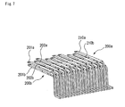
- the upper contact group 200a consists of contacts 201a to 210a as shown in Figs. 1 and 6 .
- each of the contacts 201a to 210a is a terminal substantially in an L-shape. A tip end side of each contact is received and retained in one of the terminal insertion holes 111a in the body 100, while a base end side of the contact is disposed along the rear face of the body 100.
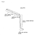
- each contact 201a is made up of the contact point portion 2011a and the contact main portion 2012a that is provided continuously from a rear end of the contact point portion 2011a and inserted into one of the terminal insertion holes 111a in the body 100.
- the base end side of each contact 201a is made up of the linking portion 2013a, provided continuously from a rear end of the contact main portion 2012a and bent at a substantially right angle so as to extend along the rear face of the body 100, and the lead portion 2014a, provided continuously from a rear end of the linking portion 2013a and bent at a substantially right angle.
- the lower contact group 200b consists of contacts 201b to 210b.
- each of the contacts 201b to 210b is a terminal in a substantially L-letter shape. A tip end side of each contact is received and retained in one of the terminal insertion holes 111b in the body 100, while a base end side of the contact is disposed along the rear face of the body 100.
- each contact 201b is made up of the contact point portion 2011b and the contact main portion 2012b that is provided continuously from a rear end of the contact point portion 2011b and inserted into one of the terminal insertion holes 111b in the body 100.
- the base end side of each contact 201b is made up of the linking portion 2013b, provided continuously from a rear end of the contact main portion 2012b and bent substantially at a right angle so as to extend along the rear face of the body 100, and the lead portion 2014b, provided continuously from a rear end of the linking portion 2013b and bent substantially at a right angle.
- the contact point portions 2011a and 2011b of the contacts 201a, 201b are contactable with contacts (not shown) of the plug of mating connector A as engaged with the body 100.
- the contact 201a is different from the contact 201b in that the linking portion 2013a is longer than the linking portion 2013b by the distance of the difference in levels between the upper and lower contact groups 200a and 200b. Moreover, the contact point portion 2011a and the contact point portion 2011b are also different from each other in length, but the details of the difference is to be described later.
- the contact point portion 2011a is received in the associated terminal guide groove 121a in the body 100
- the contact main portion 2012a is received in the associated terminal insertion holes 111a in the body 100
- the linking portion 2013a is received in the associated groove 114 in the body 100, and these parts are respectively retained in this state.
- the contact 201b is press fitted into an associated one of the terminal insertion holes 111b in the body 100 from the rear side, the contact point portion 2011b is received in the associated terminal guide groove 121b in the body 100, the contact main portion 2012b is received in the associated terminal insertion hole 111b in the body 100, and the linking portion 2013b is received in the associated groove 114 in the body 100, and these parts are respectively retained in this state.
- the lead portion 2014a of the contact 201a and the lead portion 2014b of the contact 201b are aligned with each other in the widthwise direction, and are located at a height identical to the bottom face of the base part 130 of the body 100 as shown in Fig. 4 .
- the lead portions 2014a and 2014b etc. of the alternate upper and lower contact groups 200a and 200b are aligned at the pitch distance t as shown in Fig. 11 .
- a blank region ⁇ Between each two adjacent contacts 201a to 210a and in the vicinity of the terminal insertion holes 111a and 111b in the rear face of the body 100, there exists a blank region ⁇ .
- Fig. 11 illustrates only the blank region ⁇ between the contact 201a and the contact 202a, the blank region ⁇ between the contact 202a and the contact 203a, and the end region ⁇ on a side of the contact 201a.
- the electric connector according to the present embodiment is used as a power source line and also used for transmission of single end signals and first to fifth differential signals.
- the upper and lower contact groups 200a and 200b consist of the contacts (207a, 210a, 207b, 209b and 210b) to be used as a power source line and in transmission of and single-ended signals, the contacts (201a, 202b, 205a, 205b and 208a) for plus signals to be used in transmission of first to fifth differential signals, the contacts (202a, 204a, 203b, 206b and 209a) for minus signals, and the contacts (201b, 203a, 204b, 206a and 208b) for common grounds.
- each triangular set is formed by one positive signal contact and one negative signal contact disposed at one side of the triangular arrangement and one common ground contact disposed at the opposite apex.
- the contacts for signal transmission and other use are arranged in the above-described relationship. Therefore, for the purpose of reducing a skew, etc. between adjacent contacts of each differential pair and between the differential pairs, the longitudinal relationship among the contact portions 2011a-2111a of the contacts 201a-210a and the contact portions 2011b-2111b of the contacts 201b-210b is established as shown in Fig. 9 .
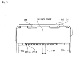
- the shield cover 300 is a metal shell which can be brought into contact with an outer peripheral shield (not shown) of the plug or mating connector A as engaged with the body 100, in use.
- the shield cover 300 has a main part 310 in a rectangular frame shape with front and rear ends thereof opened surrounding the outer periphery of the body 100, a pair of legs 320 provided as piece members formed on opposite ends of a bottom face of the shield cover main part 310, in correspondence with mounting holes provided in an external circuit board (not shown), and a back cover 330 formed as a plate member provided on the rear side of the shield cover main part 310 for openably closing the open rear end of the body 100.
- pivotal support members 311 for retaining the back cover 330 in an opened or closed state.
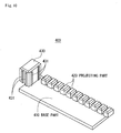
- the spacer 400 of a plate shape is made of a dielectric plastics material and, as shown in Figs. 5 and 10 , has a base part 410, eleven projecting parts 420, and the attaching part 430 as shown in Figs. 5 and 10 .
- the base part 410 is a plate member disposed to oppose the rear face of the body 100 and has an area sufficient to cover the linking portions 2013a, 2013b of the upper and lower contact groups 200a and 200b led out of the rear face of the body 100.
- the eleven projecting parts 420 are in substantially rectangular solid shapes and aligned on the base part 410, so as to be disposed respectively in the blank regions ⁇ and the end regions ⁇ .
- the attaching part 430 is in a substantially rectangular solid shape and is provided on one end of the base part 410.
- the spacer 400 is made of a material, such as nylon, having a relative permittivity larger than that of the material of the body 100.
- Each of the projecting parts 420 has a width slightly smaller than the space between the respective two adjacent contacts 201a to 210a in the upper contact group 200a.
- the attaching part 430 is provided on each side face thereof with retentive linear projections 431.
- the attaching part 430 of the spacer 400 when the attaching part 430 of the spacer 400 is inserted into the rectangular hole 113 in the body 100, the projections 431 formed on the attaching part 430 abut inner faces of the rectangular hole 113. By friction of the abutment, the spacer 400 is retained partly in the rectangular hole 113 and is generally mounted inside the cutout 112 of the body 100. In this state, the projecting parts 420 are received respectively in the clearances and on the opposite ends of the contacts 201a to 210a, that is, disposed in the blank regions ⁇ and the end regions ⁇ .
- the projecting parts 420 of the dielectric spacer 400 are respectively disposed in the blank regions ⁇ and the end regions ⁇ that are clearances between the contacts in the upper contact group 200a led out of the rear face of the body 100.
- This arrangement increases the electrostatic capacitances between each two of the contacts 201a to 210a that are disposed on opposite sides of the respective blank regions ⁇ , and accordingly the impedance is decreased.
- the magnitude of the impedance can be easily controlled by changing the material of the spacer 400 or the size, shape and the like of each of the projecting parts 420.
- the spacer 400 electrically insulates the upper and lower contact groups 200a and 200b, which are led out of the rear face of the body 100, from the back cover 330 of the shield cover 300.
- the spacer 400 electrically insulates the upper and lower contact groups 200a and 200b, which are led out of the rear face of the body 100, from the back cover 330 of the shield cover 300.
- the relative positional relations are equalized within each differential pair and between the differential pairs because of the above-described arrangements among the contacts (201a, 202b, 205a, 205b and 208a) for plus signals to be used in transmission of first to fifth differential signals, the contacts (202a, 204a, 203b, 206b and 209a) for minus signals, and the contacts (201b, 203a, 204b, 206a and 208b) for common grounds. [0053] Therefore, variation in impedance can be suppressed irrespective of the offset in levels between the upper contact group 200a and the lower contact group 200b. In other words, impedance matching is achieved at a high level within each differential pair and between the differential pairs, resulting in improved transmission characteristics of the connector.
- the contact point portions 2011a, 2011b, etc. of the contacts 201a, 201b, etc. may be subject to such a backward force as to drive the contacts 201a, 201b, etc. out of the terminal insertion holes 111a and 111b of the body 100.
- the linking portions 2013a etc. of the contacts 201a etc. are brought into abutment against the base part 410 of the spacer 400. Therefore, the contacts 201a etc. are less likely to be driven backwards than contacts in a connector not having the spacer base part 410.
- the spacer 400 is interposed between the linking portions 2013a etc. of the contacts 201a etc. and the back cover 330 of the shield cover 300, so that the contacts 201a etc. are prevented from being brought into contact with the shield cover 300 and causing electric short-circuiting.
- the connector can be improved in performance.
- the electric connector according to the present invention is not limited to the above-described embodiment, nor is it limited to a board mount type but is similarly applicable to a cable connection type. Further, the electric connector according to the present invention is not limited to a particular system of electric signal transmission, but is similarly applicable to a transmission system of unbalanced type.
- the design of the body may be appropriately modified in terms of the shape and the material, as well as the number and arrangement of the terminal receiving holes, in accordance with an application target.
- the body may be any design as long as it has a shape suitable to engage on the front side thereof with a mating connector, and as long as the body has terminal receiving holes aligned in the widthwise direction at an equal pitch distance in a plurality of rows spaced apart from one another and shifted in phase.
- the contacts may be any shape as long as they are terminals substantially of L-shape, with the tip end sides adapted to be received and retained in terminal receiving holes in the body with the base end sides being disposed along the rear face of the body, and with the lead portions on the rear ends being aligned in one line in the widthwise direction at the pitch distance t.
- the spacer is not limited in terms of the shape or the way of attachment, etc., as long as it is a dielectric body which can be disposed in the blank regions in the vicinity of the terminal receiving holes in the rear face of the body, each region being defined by the adjacent contacts with base end sides thereof spaced apart at a distance " n ⁇ t " (where n is an integer not smaller than two).
- the spacer may not be formed uniformly in terms of material, shape, thickness and the like, but may be formed differently in accordance with the variations in impedance between the respective adjacent contacts.
Landscapes
- Details Of Connecting Devices For Male And Female Coupling (AREA)
- Coupling Device And Connection With Printed Circuit (AREA)
Applications Claiming Priority (1)
| Application Number | Priority Date | Filing Date | Title |
|---|---|---|---|
| JP2007184285A JP5001734B2 (ja) | 2007-07-13 | 2007-07-13 | 電気コネクタ |
Publications (3)
| Publication Number | Publication Date |
|---|---|
| EP2015401A2 true EP2015401A2 (fr) | 2009-01-14 |
| EP2015401A3 EP2015401A3 (fr) | 2013-03-13 |
| EP2015401B1 EP2015401B1 (fr) | 2014-04-16 |
Family
ID=39863054
Family Applications (1)
| Application Number | Title | Priority Date | Filing Date |
|---|---|---|---|
| EP08252371.3A Ceased EP2015401B1 (fr) | 2007-07-13 | 2008-07-11 | Connecteur électrique |
Country Status (6)
| Country | Link |
|---|---|
| US (1) | US7704101B2 (fr) |
| EP (1) | EP2015401B1 (fr) |
| JP (1) | JP5001734B2 (fr) |
| KR (1) | KR101410365B1 (fr) |
| CN (1) | CN101345373B (fr) |
| TW (1) | TWI418097B (fr) |
Cited By (1)
| Publication number | Priority date | Publication date | Assignee | Title |
|---|---|---|---|---|
| WO2011002840A3 (fr) * | 2009-06-30 | 2011-05-26 | Molex Japan Co., Ltd. | Connecteur et dispositif d'essai de semi-conducteurs comprenant le connecteur |
Families Citing this family (16)
| Publication number | Priority date | Publication date | Assignee | Title |
|---|---|---|---|---|
| JP4795444B2 (ja) * | 2009-02-09 | 2011-10-19 | ホシデン株式会社 | コネクタ |
| JP5146346B2 (ja) * | 2009-02-10 | 2013-02-20 | ブラザー工業株式会社 | コネクタ |
| WO2011100740A2 (fr) * | 2010-02-15 | 2011-08-18 | Molex Incorporated | Connecteur à couplage différentiel |
| KR20120101908A (ko) * | 2011-03-07 | 2012-09-17 | 타이코에이엠피(유) | 휴대 단말기용 접속모듈 |
| CN102916286B (zh) * | 2011-08-02 | 2015-05-27 | 富士康(昆山)电脑接插件有限公司 | 电连接器 |
| USD851043S1 (en) * | 2015-12-03 | 2019-06-11 | Hirose Electric Co., Ltd. | Electrical connector |
| USD852142S1 (en) * | 2015-12-03 | 2019-06-25 | Hirose Electric Co., Ltd. | Electrical connector |
| CN113690654A (zh) | 2016-06-15 | 2021-11-23 | 申泰公司 | 提供接触支持和阻抗匹配特性的包覆模制引线框架 |
| CN206595424U (zh) * | 2016-10-05 | 2017-10-27 | 番禺得意精密电子工业有限公司 | 连接器 |
| US10368437B2 (en) * | 2017-04-06 | 2019-07-30 | Dell Products, L.P. | Cable assembly for an information handling system |
| KR102312443B1 (ko) | 2018-06-12 | 2021-10-12 | 주식회사 엘지에너지솔루션 | 서지 방지 기능을 가진 커넥터 및 이를 포함하는 회로기판 |
| KR102074375B1 (ko) * | 2018-09-06 | 2020-02-06 | 한국단자공업 주식회사 | 케이블 커넥터 |
| JP7003891B2 (ja) * | 2018-10-30 | 2022-01-21 | 住友電装株式会社 | 基板用コネクタ及び基板用コネクタのハウジングの製造方法 |
| KR101977616B1 (ko) * | 2018-11-27 | 2019-05-13 | 에스씨에스프로 주식회사 | 양방향 랜딩 방식의 ic 카드 소켓 |
| CN113131286B (zh) * | 2021-04-23 | 2025-05-13 | 中航光电科技股份有限公司 | 一种端子触头结构及连接器 |
| US12512615B2 (en) * | 2023-04-28 | 2025-12-30 | J.S.T. Corporation | Pin connector |
Citations (1)
| Publication number | Priority date | Publication date | Assignee | Title |
|---|---|---|---|---|
| JP2005293970A (ja) | 2004-03-31 | 2005-10-20 | Taiko Denki Co Ltd | レセプタクル |
Family Cites Families (15)
| Publication number | Priority date | Publication date | Assignee | Title |
|---|---|---|---|---|
| US4802860A (en) * | 1987-03-04 | 1989-02-07 | Hirose Electric Co., Ltd. | Surface mount type electrical connector |
| JP2558771Y2 (ja) * | 1990-11-30 | 1998-01-14 | 本多通信工業株式会社 | 面実装型コネクタ |
| US5591035A (en) * | 1994-10-06 | 1997-01-07 | The Whitaker Corporation | Electrical connector with shortened contact |
| JP2811541B2 (ja) * | 1994-11-01 | 1998-10-15 | 日本航空電子工業株式会社 | コネクタ |
| JP3926880B2 (ja) * | 1997-03-31 | 2007-06-06 | 富士通株式会社 | 多層プリント板 |
| CN2409647Y (zh) * | 1999-12-16 | 2000-12-06 | 富士康(昆山)电脑接插件有限公司 | 线缆连接器 |
| US6749444B2 (en) * | 2002-01-16 | 2004-06-15 | Tyco Electronics Corporation | Connector with interchangeable impedance tuner |
| US7044752B2 (en) * | 2002-05-24 | 2006-05-16 | Fci Americas Technology, Inc. | Receptacle |
| US7039417B2 (en) * | 2003-09-25 | 2006-05-02 | Lenovo Pte Ltd | Apparatus, system, and method for mitigating access point data rate degradation |
| WO2004001907A1 (fr) * | 2002-06-21 | 2003-12-31 | Molex Incorporated | Connecteur a reglage d'impedance haute densite presentant une structure modulaire |
| US6969267B2 (en) * | 2003-03-26 | 2005-11-29 | Intel Corporation | Land grid array socket loading device |
| CN2687897Y (zh) * | 2004-01-06 | 2005-03-23 | 富士康(昆山)电脑接插件有限公司 | 电连接器 |
| JP4201782B2 (ja) * | 2004-06-03 | 2008-12-24 | タイコエレクトロニクスアンプ株式会社 | 基板実装型電気コネクタ |
| JP4948206B2 (ja) * | 2007-03-02 | 2012-06-06 | ホシデン株式会社 | 電気コネクタ |
| JP4912244B2 (ja) * | 2007-07-13 | 2012-04-11 | ホシデン株式会社 | 電気コネクタ |
-
2007
- 2007-07-13 JP JP2007184285A patent/JP5001734B2/ja not_active Expired - Fee Related
-
2008
- 2008-05-23 TW TW097119259A patent/TWI418097B/zh not_active IP Right Cessation
- 2008-06-24 US US12/145,087 patent/US7704101B2/en active Active
- 2008-06-27 KR KR1020080061421A patent/KR101410365B1/ko not_active Expired - Fee Related
- 2008-07-11 CN CN200810130328XA patent/CN101345373B/zh not_active Expired - Fee Related
- 2008-07-11 EP EP08252371.3A patent/EP2015401B1/fr not_active Ceased
Patent Citations (1)
| Publication number | Priority date | Publication date | Assignee | Title |
|---|---|---|---|---|
| JP2005293970A (ja) | 2004-03-31 | 2005-10-20 | Taiko Denki Co Ltd | レセプタクル |
Cited By (2)
| Publication number | Priority date | Publication date | Assignee | Title |
|---|---|---|---|---|
| WO2011002840A3 (fr) * | 2009-06-30 | 2011-05-26 | Molex Japan Co., Ltd. | Connecteur et dispositif d'essai de semi-conducteurs comprenant le connecteur |
| US8905788B2 (en) | 2009-06-30 | 2014-12-09 | Molex Japan Co. Ltd. | Connector and semiconductor testing device including the connector |
Also Published As
| Publication number | Publication date |
|---|---|
| KR101410365B1 (ko) | 2014-06-19 |
| EP2015401A3 (fr) | 2013-03-13 |
| JP5001734B2 (ja) | 2012-08-15 |
| TWI418097B (zh) | 2013-12-01 |
| TW200908454A (en) | 2009-02-16 |
| EP2015401B1 (fr) | 2014-04-16 |
| US7704101B2 (en) | 2010-04-27 |
| CN101345373B (zh) | 2012-12-12 |
| KR20090007212A (ko) | 2009-01-16 |
| JP2009021165A (ja) | 2009-01-29 |
| CN101345373A (zh) | 2009-01-14 |
| US20090017693A1 (en) | 2009-01-15 |
Similar Documents
| Publication | Publication Date | Title |
|---|---|---|
| EP2015401B1 (fr) | Connecteur électrique | |
| US8333619B2 (en) | Connector | |
| US10741944B2 (en) | Electrical connector improving high-frequency characteristics | |
| EP2148399B1 (fr) | Connecteur | |
| US8672711B2 (en) | Connector including a shield case and a contact at least a part of the contact adjacent to a part of the shield case | |
| US6254435B1 (en) | Edge card connector for a printed circuit board | |
| US8727791B2 (en) | Electrical connector assembly | |
| US9478888B2 (en) | Electrical connector with low-stress, reduced-electrical-length contacts | |
| CN101032060B (zh) | 具有用于正确连接的键式装置的边缘卡连接器 | |
| JP5027907B2 (ja) | 高速電気コネクタ | |
| US20160233631A1 (en) | Electrical connector | |
| EP2015402A2 (fr) | Connecteur électrique | |
| CN1143416C (zh) | 插件边缘接头件 | |
| US20120252271A1 (en) | High speed high density connector assembly | |
| US10749289B2 (en) | Electrical connector with different length signal terminals having correction features for delayed skew | |
| CN1396681A (zh) | 通用串行总线电连接器 | |
| CN109326906A (zh) | 电接触预加载结构 | |
| US7682192B2 (en) | Electrical receptacle and circuit board with controlled skew | |
| EP2621025B1 (fr) | Procédé de réglage d'impédance de contact, contact et connecteur ayant le même | |
| EP2015400B1 (fr) | Contact, et connecteur électrique l'utilisant | |
| EP2149942A1 (fr) | Connecteur électrique | |
| US20240039195A1 (en) | Connector and connector assembly | |
| US20240413584A1 (en) | Electrical connector | |
| KR101113563B1 (ko) | 케이블 접속용 커넥터 |
Legal Events
| Date | Code | Title | Description |
|---|---|---|---|
| PUAI | Public reference made under article 153(3) epc to a published international application that has entered the european phase |
Free format text: ORIGINAL CODE: 0009012 |
|
| AK | Designated contracting states |
Kind code of ref document: A2 Designated state(s): AT BE BG CH CY CZ DE DK EE ES FI FR GB GR HR HU IE IS IT LI LT LU LV MC MT NL NO PL PT RO SE SI SK TR |
|
| AX | Request for extension of the european patent |
Extension state: AL BA MK RS |
|
| PUAL | Search report despatched |
Free format text: ORIGINAL CODE: 0009013 |
|
| AK | Designated contracting states |
Kind code of ref document: A3 Designated state(s): AT BE BG CH CY CZ DE DK EE ES FI FR GB GR HR HU IE IS IT LI LT LU LV MC MT NL NO PL PT RO SE SI SK TR |
|
| AX | Request for extension of the european patent |
Extension state: AL BA MK RS |
|
| 17P | Request for examination filed |
Effective date: 20130527 |
|
| RBV | Designated contracting states (corrected) |
Designated state(s): AT BE BG CH CY CZ DE DK EE ES FI FR GB GR HR HU IE IS IT LI LT LU LV MC MT NL NO PL PT RO SE SI SK TR |
|
| REG | Reference to a national code |
Ref country code: DE Ref legal event code: R079 Ref document number: 602008031517 Country of ref document: DE Free format text: PREVIOUS MAIN CLASS: H01R0012200000 Ipc: H01R0012720000 |
|
| GRAP | Despatch of communication of intention to grant a patent |
Free format text: ORIGINAL CODE: EPIDOSNIGR1 |
|
| AKX | Designation fees paid |
Designated state(s): DE FR GB |
|
| RIC1 | Information provided on ipc code assigned before grant |
Ipc: H01R 12/72 20110101AFI20131018BHEP |
|
| INTG | Intention to grant announced |
Effective date: 20131114 |
|
| GRAS | Grant fee paid |
Free format text: ORIGINAL CODE: EPIDOSNIGR3 |
|
| GRAA | (expected) grant |
Free format text: ORIGINAL CODE: 0009210 |
|
| AK | Designated contracting states |
Kind code of ref document: B1 Designated state(s): DE FR GB |
|
| REG | Reference to a national code |
Ref country code: GB Ref legal event code: FG4D |
|
| REG | Reference to a national code |
Ref country code: DE Ref legal event code: R096 Ref document number: 602008031517 Country of ref document: DE Effective date: 20140528 |
|
| REG | Reference to a national code |
Ref country code: DE Ref legal event code: R097 Ref document number: 602008031517 Country of ref document: DE |
|
| PLBE | No opposition filed within time limit |
Free format text: ORIGINAL CODE: 0009261 |
|
| STAA | Information on the status of an ep patent application or granted ep patent |
Free format text: STATUS: NO OPPOSITION FILED WITHIN TIME LIMIT |
|
| 26N | No opposition filed |
Effective date: 20150119 |
|
| REG | Reference to a national code |
Ref country code: DE Ref legal event code: R097 Ref document number: 602008031517 Country of ref document: DE Effective date: 20150119 |
|
| REG | Reference to a national code |
Ref country code: FR Ref legal event code: PLFP Year of fee payment: 9 |
|
| REG | Reference to a national code |
Ref country code: FR Ref legal event code: PLFP Year of fee payment: 10 |
|
| REG | Reference to a national code |
Ref country code: FR Ref legal event code: PLFP Year of fee payment: 11 |
|
| REG | Reference to a national code |
Ref country code: DE Ref legal event code: R082 Ref document number: 602008031517 Country of ref document: DE Representative=s name: ETL IP PATENTANWALTSGESELLSCHAFT MBH, DE Ref country code: DE Ref legal event code: R082 Ref document number: 602008031517 Country of ref document: DE Representative=s name: ETL IP PATENT- UND RECHTSANWALTSGESELLSCHAFT M, DE Ref country code: DE Ref legal event code: R082 Ref document number: 602008031517 Country of ref document: DE Representative=s name: ETL WABLAT & KOLLEGEN PATENT- UND RECHTSANWALT, DE |
|
| REG | Reference to a national code |
Ref country code: DE Ref legal event code: R082 Ref document number: 602008031517 Country of ref document: DE Representative=s name: ETL IP PATENTANWALTSGESELLSCHAFT MBH, DE Ref country code: DE Ref legal event code: R082 Ref document number: 602008031517 Country of ref document: DE Representative=s name: ETL IP PATENT- UND RECHTSANWALTSGESELLSCHAFT M, DE |
|
| PGFP | Annual fee paid to national office [announced via postgrant information from national office to epo] |
Ref country code: FR Payment date: 20210611 Year of fee payment: 14 |
|
| PGFP | Annual fee paid to national office [announced via postgrant information from national office to epo] |
Ref country code: GB Payment date: 20210616 Year of fee payment: 14 |
|
| PGFP | Annual fee paid to national office [announced via postgrant information from national office to epo] |
Ref country code: DE Payment date: 20220531 Year of fee payment: 15 |
|
| GBPC | Gb: european patent ceased through non-payment of renewal fee |
Effective date: 20220711 |
|
| PG25 | Lapsed in a contracting state [announced via postgrant information from national office to epo] |
Ref country code: FR Free format text: LAPSE BECAUSE OF NON-PAYMENT OF DUE FEES Effective date: 20220731 |
|
| PG25 | Lapsed in a contracting state [announced via postgrant information from national office to epo] |
Ref country code: GB Free format text: LAPSE BECAUSE OF NON-PAYMENT OF DUE FEES Effective date: 20220711 |
|
| REG | Reference to a national code |
Ref country code: DE Ref legal event code: R119 Ref document number: 602008031517 Country of ref document: DE |
|
| PG25 | Lapsed in a contracting state [announced via postgrant information from national office to epo] |
Ref country code: DE Free format text: LAPSE BECAUSE OF NON-PAYMENT OF DUE FEES Effective date: 20240201 |