EP2015378A1 - Organischer Dünnschichttransistor und Herstellungsverfahren - Google Patents
Organischer Dünnschichttransistor und Herstellungsverfahren Download PDFInfo
- Publication number
- EP2015378A1 EP2015378A1 EP20080159673 EP08159673A EP2015378A1 EP 2015378 A1 EP2015378 A1 EP 2015378A1 EP 20080159673 EP20080159673 EP 20080159673 EP 08159673 A EP08159673 A EP 08159673A EP 2015378 A1 EP2015378 A1 EP 2015378A1
- Authority
- EP
- European Patent Office
- Prior art keywords
- insulation film
- film transistor
- organic thin
- interlayer insulation
- semiconductor layer
- Prior art date
- Legal status (The legal status is an assumption and is not a legal conclusion. Google has not performed a legal analysis and makes no representation as to the accuracy of the status listed.)
- Granted
Links
Images






Classifications
-
- H—ELECTRICITY
- H10—SEMICONDUCTOR DEVICES; ELECTRIC SOLID-STATE DEVICES NOT OTHERWISE PROVIDED FOR
- H10K—ORGANIC ELECTRIC SOLID-STATE DEVICES
- H10K10/00—Organic devices specially adapted for rectifying, amplifying, oscillating or switching; Organic capacitors or resistors having potential barriers
- H10K10/40—Organic transistors
- H10K10/46—Field-effect transistors, e.g. organic thin-film transistors [OTFT]
- H10K10/462—Insulated gate field-effect transistors [IGFETs]
- H10K10/466—Lateral bottom-gate IGFETs comprising only a single gate
-
- H—ELECTRICITY
- H10—SEMICONDUCTOR DEVICES; ELECTRIC SOLID-STATE DEVICES NOT OTHERWISE PROVIDED FOR
- H10K—ORGANIC ELECTRIC SOLID-STATE DEVICES
- H10K10/00—Organic devices specially adapted for rectifying, amplifying, oscillating or switching; Organic capacitors or resistors having potential barriers
- H10K10/80—Constructional details
- H10K10/88—Passivation; Containers; Encapsulations
Definitions
- the present invention relates to an organic thin-film transistor, a method of manufacturing an organic thin-film transistor, an organic thin-film transistor array, a display panel, and a display apparatus.
- organic thin-film transistors using organic semiconductor materials have been actively studied.
- the organic thin-film transistors have advantages such a diversity in the composition of materials; high flexibility in their manufacturing method and the type of product; the area size that can be easily increased; simple layer structure and simple production process; and being manufacturable using inexpensive manufacturing equipment.
- the organic thin-film transistors may be manufactured using a printing method, a spin-coating method, a dipping method or the like that can easily form thin films and circuits, so that the organic thin-film transistors can be produced at significantly lower cost than the manufacturing cost of thin-film transistors made of Si semiconductor materials.
- an organic semiconductor layer is patterned. If the transistors are formed without patterning the organic semiconductor layer, an off-current is increased when the transistors are in operation, so that power consumption is increased. This may also cause crosstalk when displaying a display medium.
- photolithography and etching techniques are used for patterning semiconductor layers using Si semiconductor materials. For instance, patterning is performed by applying photoresist; exposing and developing a desired pattern to form a resist pattern; performing etching using the resist pattern as a mask; and removing the resist.
- the organic semiconductor layers may be patterned by using photolithography and etching techniques in the same manner as the semiconductor layers using Si semiconductor materials.
- transistor properties are highly likely to be reduced. This is because organic solvents (e.g., xylene, cellosolve-based solvents, etc.) in which novolac-based resin having naphthoquinone diazido are dissolved are usually used as a photosensitive material and the polymeric materials are often dissolved in the organic solvents.
- organic solvents e.g., xylene, cellosolve-based solvents, etc.
- novolac-based resin having naphthoquinone diazido are usually used as a photosensitive material and the polymeric materials are often dissolved in the organic solvents.
- transistor properties can be reduced more or less.
- removers e.g., ethylene glycol monobutyl ether, monoethanolamine
- Rinsing with pure water after removal of the resist may also cause damage.
- a shadow mask may be used when patterning an organic semiconductor layer using a crystalline material such as pentacene.
- a method has a limitation in the pattern size and is not suitable for patterning a large area.
- the shadow mask has a limited service life. It is therefore actually difficult to manufacture the organic thin-film transistors at significantly lower cost than the manufacturing cost of the thin-film transistors using Si semiconductor materials.
- Japanese Patent Laid-Open Publication No. 2004-297011 discloses a method of manufacturing an organic thin-film transistor appropriately selecting and using a method that applies charges to a predetermined position of a surface to be coated, applies charges of the opposite polarity to a coating material, and guides the charged material to the predetermined position due to Coulomb's force; a method that forms a recess in a predetermined position on the surface to be coated and applies a coating material such that the coating material is deposited in the recess; and a method that applies a material, forms a pattern by evaporating a solvent, and shapes the pattern using laser irradiation.
- Japanese Patent Laid-Open Publication No. 2004-141856 discloses a patterning method that forms an indent region in the surface of a substrate and deposits a liquid material in a selected location adjacent to the indent region on the substrate surface.
- the inkjet printing methods can directly draw patterns, thereby improving the material usage rate. That is, there is a possibility that patterning the organic semiconductor layers using the inkjet printing methods can achieve simplification of the manufacturing process, improvement in the production yield, and cost reduction.
- an organic semiconductor ink can be prepared by dissolving the polymeric material in organic solvent, so that an inkjet printing method can be used for patterning.
- Reducing the size of ink droplets may be a solution. But, reduction in the droplet size is technically difficult, has stability issues, and easily results in clogged nozzles and ejection of ink droplets at an angle.
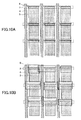
- any of the nozzles ejects ink droplets even at a slight angle, it may be possible to form patterns at low resolution but not at high resolution. For example, it is not possible to pattern an organic semiconductor layer in island shapes with high precision as shown in FIG. 10A , and an inaccurate pattern as shown in FIG. 10B is formed. It is to be noted that, in organic thin-film transistor arrays shown in FIGS. 10A and 10B , a gate electrode 2, a gate insulation film (not shown), source and drain electrodes 4 and 5, and an organic semiconductor layer 6 are stacked in this order on a glass substrate (not shown).
- the present invention is directed to provide an organic thin-film transistor that allows reduction of off-current and a method of manufacturing the organic thin-film transistor.
- the present invention is also directed to provide an organic thin-film transistor array having the organic thin-film transistor, a display panel having the organic thin-film transistor array, and a display apparatus having the display panel.
- an organic thin-film transistor that comprises a gate electrode formed on a substrate; a gate insulation film formed on the gate electrode; a source electrode and a drain electrode formed, with a gap therebetween, at least over the gate electrode on which the gate insulation film is formed; an organic semiconductor layer formed in a region including the gap; an interlayer insulation film formed to cover the organic semiconductor layer; and a conductive layer formed on the interlayer insulation film and connected to the drain electrode. A part of the organic semiconductor layer is formed on the interlayer insulation film.
- a method of manufacturing the above-described organic thin-film transistor comprises a step of forming the gate electrode on the substrate; a step of forming the gate insulation film on the gate electrode; a step of forming the source electrode and the drain electrode, with the gap therebetween, at least over the gate electrode on which the gate insulation film is formed; a step of forming a first portion of the interlayer insulation film on the substrate on which the source electrode and the drain electrode are formed; a step of forming the organic semiconductor layer in contact with the first portion of the interlayer insulation film in a region including the gap; and a step of forming a second portion of the interlayer insulation film at least over the organic semiconductor layer.
- an organic thin-film transistor array that comprises the above-described organic thin-film transistor.
- a display panel that comprises the above-described organic thin-film transistor array and a display device.
- a display apparatus that comprises the above-described display panel.
- an organic thin-film transistor that allows reduction of off-current and a method of manufacturing the organic thin-film transistor.
- FIG. 1 illustrates an example of an organic thin-film transistor array 10 according to an embodiment of the present invention.
- the organic thin-film transistor array 10 includes an organic thin-film transistor 10a.
- a gate electrode 12 is formed on a glass substrate 11, and a gate insulation film 13 is formed on the gate electrode 12.
- a source electrode 14 and a drain electrode 15 are formed, with a gap therebetween, on the gate insulation film 13.
- the gap between the source electrode 14 and the drain electrode 15 is formed on the gate electrode 12.
- An organic semiconductor layer 16 is formed to fill the gap between the source electrode 14 and the drain electrode 15.
- An interlayer insulation film 17 is formed to cover the organic semiconductor layer 16.
- a part of the organic semiconductor layer 16 is formed on the interlayer insulation film 17.
- a conductive layer 18 connected to the drain electrode 15 is formed on the interlayer insulation film 17.
- a method of manufacturing the organic thin-film transistor array 10 is described below with reference to FIGS. 2A - 2E .
- the gate electrode 12, the gate insulation film 13, and the source and drain electrodes 14 and 15 are stacked in this order on the glass substrate 11 (see FIG. 2A ).
- first portions 17a of the interlayer insulation film 17 are formed one on each side of the gap between the source electrode 14 and the drain electrode 15 (see FIG. 2B ).
- the organic semiconductor layer 16 is formed to fill the gap and be in contact with the first portions 17a of the interlayer insulation film 17 (see FIG. 2C ). This improves the patterning accuracy of the organic semiconductor layer 16.
- the first portions 17a of the interlayer insulation film 17 may partly cover the source electrode 14.
- the rest (second portion 17b) of the interlayer insulation film 17 is formed on the organic semiconductor layer 16 (see FIG. 2D ).
- the conductive layer 18 is formed on the interlayer insulation film 17 so as to be connected to the drain electrode 15 (see FIG. 2E ).
- the gate electrode 12, the source electrode 14, and the drain electrode 15 may preferably be formed using a printing method such as a screen printing method, an inkjet printing method, a flexographic printing method, a gravure printing method, and an offset printing method.
- a printing method such as a screen printing method, an inkjet printing method, a flexographic printing method, a gravure printing method, and an offset printing method.
- Metal ink with metal particles dispersed therein may preferably be used in this process. Examples of metal particles include Au, Ag, Cu, Pt, Pd, Ni, Ir, Rh, Co, Fe, Mn, Cr, Zn, Mo, W, Ru, In, and Sn. These metal particles may be used alone or as a mixture of two or more of them. More preferable are Au, Ag, Cu, and Ni in terms of electric resistance, thermal conductivity, and corrosion resistance.
- the metal ink metal particles of average particle size ranging from a few nanometers to several tens of nanometers are uniformly dispersed in a solvent. It is possible to sinter such metal particles because metal particles having smaller diameters are more easily affected by atoms at the highly active surface. Therefore, it is possible to print with such a metal ink using an inkjet printing method and sinter the metal particles, thereby directly drawing electrodes.
- the metal ink may preferably have a surface tension of about 30 mN/m.
- the viscosity of the metal ink may preferably be in the range of 2 - 13 mPa ⁇ s, more preferably in the range of 7 - 10 mPa ⁇ s.
- a metal ink not having suitable surface tension and viscosity may cause ejection failure or poor performance such as difficulty in forming round droplets, and may also result in ligaments with increased length.
- the metal ink has drying properties but prevents the metal particles from being solidified due to volatilization of solvent during ejection of the metal ink.
- the gate electrode 12, the source electrode 14, and the drain electrode 15 may be formed of conductive polymers.
- conductive polymers include polythiophene, polyaniline, polypyrrole, polyparaphenylene, and polyacetylene. These polymers subjected to a doping process may also be used as conductive polymers.
- a complex (PEDOT/PSS) of polyethylenedioxythiophene (PEDOT) and polystyrenesulfonate(PSS) may be preferable in terms of electric conductivity, stability, heat resistance, etc.
- the electric properties of the conductive polymers can be adjusted by changing the degree of polymerization and the structure. Furthermore, the conductive polymers can form electrodes at low temperatures because no sintering process is required.
- the first portions 17a of the interlayer insulation film 17 formed in the step of FIG. 2B are lines substantially parallel to the channel as shown in FIG. 3A .
- the first portions 17a of the interlayer insulation film 17 can prevent, upon forming the organic semiconductor layer 16 using an inkjet printing method, ink from being ejected off the target positions and from spreading on the target surface even if the ink is improperly ejected.
- the organic semiconductor layer 16 is formed on the region between the first portions 17a of the interlayer insulation film 17, so that leakage of current via the organic semiconductor layer 16 can be prevented, thereby reducing the off-current and improving the on-off ratio.
- the patterning properties of the organic semiconductor layer 16 are significantly improved, thereby preventing adjacent transistors from adversely affecting each other.
- the alignment accuracy in forming the organic semiconductor layer 16 is required only in one direction, so that the throughput and production yield can be improved.
- the first portions 17a of the interlayer insulation film 17 may be lines substantially perpendicular to the channel as shown in FIG. 3B .
- the first portions 17a of the interlayer insulation film 17 are formed in regions excluding the channel region in the longitudinal direction.
- the first portions 17a of the interlayer insulation film 17 prevent, upon forming the organic semiconductor layer 16 using an inkjet printing method, ink from being ejected off the target positions and from spreading on the target surface even if the ink is improperly ejected.
- the organic semiconductor layer 16 is formed on the region between the first portions 17a of the interlayer insulation film 17 and therefore can prevent leakage of current via the organic semiconductor layer 16, thereby reducing the off-current and improving the on-off ratio.
- the patterning properties of the organic semiconductor layer 16 are significantly improved, thereby preventing adjacent transistors from adversely affecting each other.
- the alignment accuracy in forming the organic semiconductor layer 16 is required only in one direction, so that the throughput and production yield can be improved.
- the first portions 17a of the interlayer insulation film 17 formed in the step of FIG. 2B may be a combination of lines substantially parallel to the channel and lines substantially perpendicular to the channel, i.e., may be arranged in a lattice form. With this arrangement, the alignment accuracy in forming the organic semiconductor layer 16 does not need to be high, so that the throughput and production yield can be improved.
- the first portions 17a of the interlayer insulation film 17 may preferably be formed in a single step, although they may be formed in plural steps. In the case of forming the first portions 17a of the interlayer insulation film 17, after forming first lines, second lines orthogonal to the first lines may be formed. Alternatively, after forming first lines, dots may be formed between the first lines.
- the organic semiconductor layer 16 may preferably be formed using a printing method such as a screen printing method, an inkjet printing method, a flexographic printing method, a gravure printing method, and an offset printing method.
- An inkjet printing method is more preferable in terms of patterning accuracy, cost, and solubility.
- the organic semiconductor layer 16 may preferably contain an organic semiconductor material soluble in an organic solvent.
- the organic semiconductor layer 16 can be formed using an organic semiconductor ink having such an organic semiconductor material dissolved in an organic solvent.
- Non-exclusive examples of organic semiconductor material include polymeric materials, oligomer materials, and low-molecular materials that are soluble in an organic solvent.
- a polymeric material having a triallyl amine structure is preferable, and a compound represented by the following Formula (1) is more preferable.
- the compound of Formula (1) is a non-oriented polymeric material and its variation in properties is small regardless of the layer shape and the deposition method.
- the organic semiconductor layer 16 In the case of the related-art transistor array, if the organic semiconductor layer 16 is formed using an inkjet printing method, it is difficult to form a high-precision pattern as shown in FIG. 10A , and an imperfect pattern as shown in FIG. 10B is likely to be formed. Especially, an imperfect pattern is more likely to be formed when patterning a large area.
- the organic semiconductor layer 16 might be formed not only in the channel region but also in a non-channel region between the source electrode 14 and the drain electrode 15. Furthermore, the organic semiconductor layer 16 might not be divided by organic thin-film transistors of an organic thin-film transistor array so that adjacent organic thin-film transistors adversely affect each other via the organic semiconductor layer 16.
- the organic semiconductor layer 16 is imperfectly patterned because of influence due to a variation in the head properties, droplets ejected from nozzles at an angle, and the like. It is difficult to make all the nozzles have the same ejection conditions. Moreover, the drying conditions after ejection of droplets differ depending on the shape of the pattern, and the ejected droplets spread differently depending on the drying conditions. If a polymer solution is used as an ink for the organic semiconductor layer 16, a variation in the ejection speed due to changes in the properties may also make it difficult to form a pattern with high precision.
- the organic semiconductor layer 16 is formed in contact with the fist portions 17a of the interlayer insulation film 17 and thus can be physically divided by the first portions 17a of the interlayer insulation film 17. Therefore the first portions 17a can block the leakage current, thereby preventing an increase of the off-current.
- the thickness of an organic semiconductor layer formed in island shapes using an inkjet printing method varies greatly due to a coffee stain effect.
- the coffee stain phenomenon increases the concentration of solute at the edge of a spread droplet after ejection due to evaporation of solvent at the edge of the droplet, and thus makes the thickness greater at the edge and less at the center.
- the variation in the thickness due to this phenomenon increases the off-current and shifts a threshold voltage V th , resulting in increased variation in the transistor properties.
- the organic semiconductor layer 16 is formed in contact with the first portions 17a of the interlayer insulation film 17, it is possible to prevent the coffee stain phenomenon, thereby improving the uniformity in the thickness of the organic semiconductor layer 16. As a result, it is possible to prevent shifts of the threshold voltage V th and reduce the variation in the transistor properties.
- the second portions 17b of the interlayer insulation film 17 are formed on the organic semiconductor layer 16 after forming the first portions 17a shown in FIG. 3C .
- the interlayer insulation film 17 having through holes is formed.
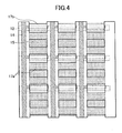
- the second portions 17b of the interlayer insulation film 17 are formed in regions on and off the organic semiconductor layer 16, so that an interlayer insulation film 17 similar to the one that is shown in FIG. 4 can be formed.
- a printing method such as a screen printing method, an inkjet printing method, a flexographic printing method, a gravure printing method, and an offset printing method may preferably be used for forming the first portions 17a and the second portions 17b of the interlayer insulation film 17, and screen printing is more preferably used. This improves the throughput, reduces the number of manufacturing steps, and reduces costs compared to using a photolithographic technique.
- the first portions 17a and the second portions 17b of the interlayer insulation film 17 may be formed using the same material or may be formed using different materials.
- the interlayer insulation film 17 may preferably contain a binder resin and particles.
- binder resin include polyvinyl alcohol resin, polyvinyl acetal resin, acrylic resin, ethyl cellulose resin, polyethylene, polystyrene, and polyamide. These materials may be used alone or as a mixture of two or more of them.
- the particles may be any organic or inorganic particles that can exist as particles in the interlayer insulation film 17.
- inorganic particles may be preferable because the inorganic particles are easily controlled in size and are dispersible in solvent.
- organic particle include carbon black, azoic pigment, phthalocyanine based pigment, and perylene based pigment. These organic particles may be used alone or as a mixture of two or more of them.
- inorganic particles include metal oxide, metal hydroxide, and metal complex such as silica, alumina, titanium oxide, zinc oxide, and barium titanate. These inorganic particles may be used alone or as a mixture of two or more of them.
- the particles may be porous particles, such as mesoporous silica, having mesoporous or porous particles having a microporous structure.
- an insulating paste may be used, which is prepared by mixing a binder resin and particles into a solvent and optionally adding dispersant, plasticizer, and viscosity modifier.
- the mixture ratio between the binder resin and the particles is not particularly limited and may be appropriately adjusted to make the paste have suitable physical properties in accordance with a pattern to be formed. To ensure flexibility of the interlayer insulation film 17, it is preferable to increase the proportion of the binder resin.
- the interlayer insulation film 17 block light absorbable by the organic semiconductor layer 16.
- the interlayer insulation film 17 may preferably contain a material that can absorb and/or block such light.
- the material capable of absorbing the light absorbable by the organic semiconductor layer 16 may be any material that can maintain the insulation properties of the interlayer insulation film 17, such as, but not limited to, metal oxide, metal hydroxide, metal complex, colored particles (carbon black, azoic pigment, phthalocyanine based pigment, perylene based pigment, etc.), and dye (aniline black, indigo, etc.). These materials may be used alone or as a mixture of two or more of them.
- the material capable of reflecting the light absorbable by the organic semiconductor layer 16 may be any material that can maintain the insulation properties of the interlayer insulation film 17, such as, but not limited to, white pigments including titanium oxide and zinc oxide. These materials may be used alone or as a mixture of two or more of them.
- FIG. 11 is a graph showing the ultraviolet-visible absorption spectrum of a 40 nm thick film of a compound represented by Formula (1).
- the graph of FIG. 11 indicates that the compound of Formula (1) tends to absorb light of 600 nm wavelength or less.
- polymeric materials having a triallyl amine structure absorb light of 600 nm wavelength or less. Therefore, in the case where a polymeric material having a triallyl amine structure is used as the organic semiconductor material, the interlayer insulation film 17 is preferably capable of blocking light of 600 nm wavelength or less. Such an interlayer insulation film 17 can prevent the transistor properties of the organic thin-film transistor array 10 from degrading over time.
- the interlayer insulation film 17 block oxygen and moisture.
- the oxygen transmission rate and water vapor transmission rate of the interlayer insulation film 17 may be suitably selected depending on the material, etc., of the organic semiconductor layer 16.
- the oxygen transmission rate and the water vapor transmission rate of an organic EL panel having the organic thin-film transistor array 10 are preferably less than 10 -2 cc/m 2 /day/atm/0.1 mm and less than 10 -5 g/m 2 /day/atm/0.1 mm, respectively.
- Such an organic EL panel can prevent degradation of its properties over time.
- the organic semiconductor layer 16 is formed of, e.g., a highly weather-resistant polymeric material having a triallyl amine structure, the upper limits of the oxygen transmission rate and the water vapor transmission rate of the organic EL panel can be increased.
- the interlayer insulation film 17 as described above can also prevent the properties of the organic thin-film transistor array 10 from degrading due to photoinduced oxidation.
- the interlayer insulation film 17 may preferably contain a material soluble in a solvent that does not dissolve or swell the organic semiconductor layer 16. This prevents degradation of the organic semiconductor layer 16 during formation of the interlayer insulation film 17.
- Non-exclusive examples of solvent that does not dissolve or swell the organic semiconductor layer 16 formed of a polymeric material having a triallyl amine structure include ethylene glycol butyl ether, ethylene glycol hexyl ether, dipropylene glycol butyl ether, dipropylene glycol methyl ether acetate, tripropylene glycol methyl ether, diethylene glycol butyl ether, ⁇ -terpineol, ethylene alcohol, isopropyl alcohol, 2,2,4-trimethyl-1, and 3-pentanediol monoisobutylate. These materials may be used alone or as a mixture of two or more of them.
- binder resin of the interlayer insulation film 17 that are soluble in these solvents include polyvinyl alcohol resin, polyvinyl acetal resin, acrylic resin, ethyl cellulose resin, polyethylene, polystyrene, and polyamide. Theses materials may be used alone or as a mixture of two or more of them.
- the conductive layer 18 is formed in and over the through hole and on the interlayer insulation film 17 so as to be connected to the drain electrode 15.
- the conductive layer 18 may be formed by patterning a thermocuring paste containing silver using a screen printing method.
- an organic thin-film transistor array of an embodiment of the present invention can be manufactured with a reduced number of manufacturing steps and at low cost.
- Display panels such as electrophoresis panels, liquid crystal panels, and organic EL panels may be formed by combining an organic thin-film transistor array of an embodiment of the present invention, which is used as an active matrix substrate, and display devices such as electrophoresis display devices, liquid crystal display devices, and organic EL display devices.
- FIG. 12 illustrates an electrophoresis panel 20 as an example of a display panel according to an embodiment of the present invention.
- a method of manufacturing the display panel 20 is described below.
- a gate electrode (scanning line) 12 is formed on a film substrate (or a thin-film SUS substrate) 11 by inkjet printing using an Ag ink having Ag particles dispersed therein.
- polyamide acid is applied onto the gate electrode 12 using a spin coating method and is heated, thereby forming a gate insulation film 13.
- ultraviolet rays are irradiated onto the gate insulation film 13 through a photomask, thereby forming a high energy pattern on the surface.
- a source electrode (signal line) 14 and a drain electrode 15 are formed on the high energy pattern by inkjet printing using an Ag ink having Ag particles dispersed therein.
- First portions 17a of an interlayer insulation film 17 are formed by screen printing using an insulation paste.
- An organic semiconductor layer 16 is formed in contact with the first portions 17a of the interlayer insulation film 17 by screen printing using an organic semiconductor ink.
- Second portions 17b of the interlayer insulation film 17 are formed on the organic semiconductor layer 16 by screen printing using an insulation paste.
- a conductive layer 18 is formed so as to be connected to the drain electrode 15 by screen printing using a conductive paste.
- An organic thin-film transistor array 10 can be formed with the steps described above.
- a transparent conductive film 21b of ITO is formed on a film substrate 21a by sputtering, thereby forming a transparent conductive coated film substrate 21.
- a mixture of titanium oxide, silicone macromer/methacrylic acid copolymer, silicone polymer graft carbon black, and silicone oil is dispersed by ultrasonic waves to obtain a dispersion liquid of black and white particles.
- Microcapsules 22a are formed from the dispersion liquid of black and white particles by a complex coacervation method using gelatin and Arabic gum.
- the microcapsules 22a are dispersed in a solution of urethane resin 22b to obtain a dispersion liquid.
- the dispersion liquid is spread onto the transparent conductive coated film substrate 21 to form electrophoresis devices 22.
- the electrophoresis devices 22 are connected to the conductive layer 18 of the organic thin-film transistor array 10, so that the electrophoresis panel 20 having memory properties and flexibility can be formed.
- a liquid crystal panel can be formed by connecting an organic thin-film transistor array of an embodiment of the present invention to a transparent conductive coated substrate with a silica spacer interposed therebetween, and filling the gap with a liquid crystal material.
- the transparent conductive coated substrate used herein has an alignment film subjected to a rubbing process.
- An organic EL panel can be formed by forming an organic EL device in an organic thin-film transistor array of an embodiment of the present invention and disposing an atmospheric shield.
- FIG. 13 shows an example of a display apparatus 30 according to an embodiment of the present invention.
- the display apparatus 30 includes an electrophoresis panel 20, an information input unit 31 configured to input information of an image to be displayed to the electrophoresis panel 20, a casing 32, a drive circuit (not shown), an arithmetic circuit (not shown), an internal memory (not shown), and a power supply unit (not shown) configured to supply power to the electrophoresis panel 20 and the information input unit 31.
- a gate electrode (scanning line) 12 and a source electrode (signal line) 14 of the electrophoresis panel 20 form a dot matrix, and turn on the specified dots to display an image as a whole.
- the power supply unit may be an internal power supply such as a battery or may be a power receiving unit such as a socket for receiving power from an external power supply.
- the display apparatus of an embodiment of the present invention may be any apparatus that includes a display panel of an embodiment of the present invention and a unit that supplies power to the display panel, and may include, but is not limited to, portable terminals such as PDAs and electronic book terminals.
- Polyamide acid was applied onto a glass substrate 11 by spin coating and was heated at 280 °C to form an insulation film 19 of 200 nm thickness. Then, ultraviolet rays were irradiated through a photomask using a UV lamp (irradiation volume: 7 J/cm 2 ) to form a high energy pattern on the surface. Then, an Ag ink having Ag particles dispersed therein was ejected onto the high energy pattern using an inkjet printing method and was sintered at 280 °C to form a gate electrode 12 of 100 nm thickness. Polyamide acid was applied onto the gate electrode 12 by spin coating and was heated at 280 °C to form a gate insulation film 13 of 500 nm thickness.
- UV rays were irradiated through a photomask using a UV lamp (irradiation volume: 7 J/cm 2 ) to form a high energy pattern on the surface.
- an Ag ink was ejected onto the high energy pattern using an inkjet printing method and was sintered at 280 °C to form a source electrode 14 and a drain electrode 15 of 100 nm thickness.
- the channel width was 140 ⁇ m and the channel length was 10 ⁇ m.
- An organic semiconductor ink having a compound of Formula (1) dissolved in tetralin was applied using an inkjet printing method to form an island-shaped organic semiconductor layer 16 (see FIG. 10B ). Then an insulation paste containing polyvinyl butyral resin, a silica filler, and ethylene glycol hexyl ether was printed using a screen printing method and was dried to form an interlayer insulation film 17 that covers the organic semiconductor layer 16. Then a thermocuring paste containing silver was printed using a screen printing method and was dried to form a conductive layer 18 connected to the drain electrode 15. Thus an organic thin-film transistor array was obtained (see FIG. 6 ).
- Polyamide acid was applied onto a glass substrate 11 by spin coating and was heated at 280 °C to form an insulation film 19 of 200 nm thickness. Then, ultraviolet rays were irradiated through a photomask using a UV lamp (irradiation volume 7 J/cm 2 ), thereby forming a high energy pattern on the surface. Then, an Ag ink having Ag particles dispersed therein was ejected onto the high energy pattern using an inkjet printing method and was sintered at 280 °C to form a gate electrode 12 of 100 nm thickness. Polyamide acid was applied onto the gate electrode 12 by spin coating and was heated at 280 °C to form a gate insulation film 13 of 500 nm thickness.
- UV rays were irradiated through a photomask using a UV lamp (irradiation volume: 7 J/cm 2 ) to form a high energy pattern on the surface.
- an Ag ink was ejected onto the high energy pattern using an inkjet printing method and was sintered at 280 °C to form a source electrode 14 and a drain electrode 15 of 100 nm thickness.
- the channel width was 140 ⁇ m and the channel length was 10 ⁇ m.
- an insulation paste containing polyvinyl butyral resin, a silica filler, and ethylene glycol hexyl ether was printed using a screen printing method and was dried to form first portions 17a of an interlayer insulation film 17 to be lines parallel to the channel (see FIG. 2B and FIG. 3A ).
- An organic semiconductor ink having a compound of Formula (1) dispersed in tetralin was applied using an inkjet printing method to form an organic semiconductor layer 16 in contact with the first portions 17a of the interlayer insulation film 17.
- the same insulation paste as the insulation paste of the first portions 17a of the interlayer insulation film 17 was printed using a screen printing method to form second portions 17b of the interlayer insulation film 17 on the organic semiconductor layer 16.
- the interlayer insulation film 17 had an oxygen transmission rate of 600 cc/m 2 /day/atm/0.1 mm and a water vapor transmission rate of 50 g/m 2 /day/atm/ 0.1 mm. Then a thermocuring paste containing silver was printed using a screen printing method and was dried to form a conductive layer 18 connected to the drain electrode 15. Thus an organic thin-film transistor array was obtained (see FIG. 7 ).
- An organic thin-film transistor array was obtained in the same manner as Example 1 except that the first portions 17a of the interlayer insulation film 17 were formed as lines perpendicular to the channel (see FIG. 3B ).
- An organic thin-film transistor array was obtained in the same manner as Example 1 except that the first portions 17a of the interlayer insulation film 17 were formed as lines parallel to and perpendicular to the channel, i.e., in a lattice form (see FIG. 2B and FIG. 3C ).
- the transistor properties of the obtained organic thin-film transistor arrays were measured in an atmosphere containing less than 1 ppm oxygen and less than 1 ppm moisture.
- the drain voltage V ds was -20 V and the gate voltage V g was scanned from +20 V to -20 V.
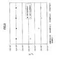
- the graph of FIG. 8 shows the measurement results of the drain currents I ds (on-currents) flowed when V g was -20 V and the drain currents I ds (off-currents) when V g was +20 V. More specifically, the on-currents of Comparative Example 1 and Examples 1 - 3 were -1.0 ⁇ 10 -8 A, -9.0 ⁇ 10 -9 A. - 1.0 ⁇ 10 -8 A, and -9.0 ⁇ 10 -9 A, respectively.
- Comparative Example 1 and Examples 1 - 3 were -5.4 ⁇ 10 -11 A, -2.1 ⁇ 10 -12 A, - 8.0 ⁇ 10 -13 A, and -9.0 ⁇ 10 -13 A, respectively.
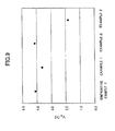
- the threshold voltages V th of Comparative Example 1 and Examples 1 - 3 were 4.11 V, 3.63 V, 4.13 V, and 1.82 V, respectively.
- the organic thin-film transistors of Examples 1 and 2 had the off-currents lower than the off-current of the organic thin-film transistor of Comparative Example 1 and therefore had improved on-off ratios. This suggests that the organic thin-film transistors of Examples 1 and 2 have better transistor properties.
- the organic thin-film transistor of Example 3 had V th lower than V th of Examples 1 and 2. This suggests that the organic thin-film transistor of Example 3 has further better transistor properties.
- FIG. 14 shows the evaluation result.
- the mobility of the organic thin-film transistor array before irradiation of light was 100%.
- the mobility of Samples B and C decreased as the duration of irradiation increased.
- the transistor properties of Sample A did not significantly decrease with the increase of duration of irradiation.
- An organic thin-film transistor array was obtained in the same manner as Example 4 except that an insulation paste containing polyvinyl butyral resin, a silica filler, aniline black, and ethylene glycol hexyl ether was used for forming the interlayer insulation film 17.
- Light having wavelength in a range of 300 - 1400 nm was irradiated onto the organic thin-film transistor array of Example 4 using a light source with an illuminance of 100,000 lux.
- the mobility of the organic thin-film transistor array of Example 4 was measured.
- the mobility was measured with the drain voltage V ds of -20 V and the gate voltage V g varying from +20 V to -20 V.
- FIG. 14 shows the evaluation result.
- the mobility of the organic thin-film transistor array before irradiation of light was 100%. Similar to Sample A, the transistor properties of the organic thin-film transistor array of Example 4 did not significantly decrease with the increase of duration of irradiation.
- An organic thin-film transistor array was obtained in the same manner as Example 3 except that the second portions 17b were not formed on the organic semiconductor layer 16.
- a high-humidity test was performed on the organic thin-film transistor arrays of Example 3 and Comparative Example 2 in a 25 °C, 85% RH environment. Then the mobility was measured in the atmosphere. The mobility was measured with the drain voltage V ds of -20 V and the gate voltage V g varying from +20 V to -20 V.
- FIG. 15 shows the evaluation result.
- the mobility of the organic thin-film transistor array before the high-humidity test was 100%.
- the mobility of the organic thin-film transistor array of Comparative Example 2 decreased as the duration of the test increased.
- the organic thin-film transistor array of Example 3 maintained the transistor properties regardless of the increase of duration of the test.
- a transparent conductive film 21b of ITO Indium Tin Oxide was formed on a film substrate 21a by sputtering, thereby forming a transparent conductive coated film substrate 21.
- Microcapsules 22a were formed from the dispersion liquid of black and white particles by a complex coacervation method using gelatin and Arabic gum. The average particle diameter of the microcapsules 22a was about 60 ⁇ m.
- the microcapsules 22a were dispersed in a solution of urethane resin 22b to obtain a dispersion liquid.
- the dispersion liquid was spread onto the transparent conductive coated film substrate 21 to form electrophoresis devices 22.
- the electrophoresis devices 22 were connected to the conductive layer 18 of the organic thin-film transistor array 10 of Example 1, so that an electrophoresis panel was obtained (see FIG. 16 ).
Landscapes
- Thin Film Transistor (AREA)
Applications Claiming Priority (2)
| Application Number | Priority Date | Filing Date | Title |
|---|---|---|---|
| JP2007182446 | 2007-07-11 | ||
| JP2008070379A JP5277675B2 (ja) | 2007-07-11 | 2008-03-18 | 有機薄膜トランジスタの製造方法 |
Publications (2)
| Publication Number | Publication Date |
|---|---|
| EP2015378A1 true EP2015378A1 (de) | 2009-01-14 |
| EP2015378B1 EP2015378B1 (de) | 2019-09-04 |
Family
ID=39673183
Family Applications (1)
| Application Number | Title | Priority Date | Filing Date |
|---|---|---|---|
| EP08159673.6A Not-in-force EP2015378B1 (de) | 2007-07-11 | 2008-07-04 | Organischer Dünnschichttransistor und Herstellungsverfahren |
Country Status (2)
| Country | Link |
|---|---|
| US (1) | US20090014716A1 (de) |
| EP (1) | EP2015378B1 (de) |
Families Citing this family (9)
| Publication number | Priority date | Publication date | Assignee | Title |
|---|---|---|---|---|
| JP4730623B2 (ja) * | 2008-07-24 | 2011-07-20 | ソニー株式会社 | 薄膜トランジスタ、薄膜トランジスタの製造方法、および電子機器 |
| DE102008036837A1 (de) | 2008-08-07 | 2010-02-18 | Epcos Ag | Sensorvorrichtung und Verfahren zur Herstellung |
| JP5446982B2 (ja) * | 2009-05-01 | 2014-03-19 | 株式会社リコー | 画像表示パネル及び画像表示装置 |
| JP5370189B2 (ja) * | 2010-02-04 | 2013-12-18 | セイコーエプソン株式会社 | 電気光学装置用基板、電気光学装置及び電子機器 |
| JP2011164196A (ja) * | 2010-02-05 | 2011-08-25 | Seiko Epson Corp | 電気光学装置用基板、電気光学装置及び電子機器 |
| CN103779202B (zh) * | 2014-01-27 | 2016-12-07 | 深圳市华星光电技术有限公司 | 像素结构及其制作方法和显示面板 |
| JP2017207816A (ja) * | 2016-05-16 | 2017-11-24 | 双葉電子工業株式会社 | タッチパネル |
| JP2020062834A (ja) * | 2018-10-18 | 2020-04-23 | 株式会社ミマキエンジニアリング | 印刷装置、印刷方法、パウダリング装置、及びパウダリング方法 |
| JP7322838B2 (ja) * | 2020-09-03 | 2023-08-08 | 株式会社村田製作所 | 電子部品および電子部品モジュール |
Citations (7)
| Publication number | Priority date | Publication date | Assignee | Title |
|---|---|---|---|---|
| WO2001095384A1 (en) * | 2000-06-03 | 2001-12-13 | The University Of Liverpool | A method of electronic component fabrication and an electronic component |
| EP1263062A2 (de) * | 2001-06-01 | 2002-12-04 | Sel Semiconductor Energy Laboratory Co., Ltd. | Organische Halbleiteranordnung und ihr Herstellungsverfahren |
| JP2004141856A (ja) | 2002-07-26 | 2004-05-20 | Seiko Epson Corp | パターニング方法 |
| JP2004297011A (ja) | 2003-03-28 | 2004-10-21 | Matsushita Electric Ind Co Ltd | 有機トランジスタの製造方法、及び有機el表示装置の製造方法 |
| US20070023837A1 (en) * | 2005-07-27 | 2007-02-01 | Samsung Electronics Co., Ltd. | Thin film transistor substrate and method of making the same |
| US20070114524A1 (en) * | 2005-11-19 | 2007-05-24 | Joon-Hak Oh | Display device and manufacturing method thereof |
| US20070134857A1 (en) * | 2005-12-13 | 2007-06-14 | Suh Min-Chul | Method of preparing organic thin film transistor, organic thin film transistor, and organic light-emitting display device including the organic thin film transistor |
Family Cites Families (9)
| Publication number | Priority date | Publication date | Assignee | Title |
|---|---|---|---|---|
| TWI292066B (de) * | 2001-03-20 | 2008-01-01 | Chi Mei Optoelectronics Corp | |
| JP4148501B2 (ja) * | 2002-04-02 | 2008-09-10 | 三井金属鉱業株式会社 | プリント配線板の内蔵キャパシタ層形成用の誘電体フィラー含有樹脂及びその誘電体フィラー含有樹脂を用いて誘電体層を形成した両面銅張積層板並びにその両面銅張積層板の製造方法 |
| US20080160447A1 (en) * | 2003-09-22 | 2008-07-03 | Willi-Kurt Gries | Photopolymer Printing Plate Precursor |
| JP4100351B2 (ja) * | 2004-02-09 | 2008-06-11 | セイコーエプソン株式会社 | 薄膜トランジスタの製造方法 |
| JP2006352083A (ja) * | 2005-05-18 | 2006-12-28 | Ricoh Co Ltd | 有機薄膜トランジスタ及びアクティブマトリックス表示装置 |
| KR20070033144A (ko) * | 2005-09-21 | 2007-03-26 | 삼성전자주식회사 | 표시장치와 표시장치의 제조방법 |
| JP2007103584A (ja) * | 2005-10-03 | 2007-04-19 | Ricoh Co Ltd | トランジスタ素子、表示装置およびこれらの製造方法 |
| KR101240657B1 (ko) * | 2006-04-28 | 2013-03-08 | 삼성디스플레이 주식회사 | 표시장치와 그 제조방법 |
| KR100801961B1 (ko) * | 2006-05-26 | 2008-02-12 | 한국전자통신연구원 | 듀얼 게이트 유기트랜지스터를 이용한 인버터 |
-
2008
- 2008-06-23 US US12/144,079 patent/US20090014716A1/en not_active Abandoned
- 2008-07-04 EP EP08159673.6A patent/EP2015378B1/de not_active Not-in-force
Patent Citations (7)
| Publication number | Priority date | Publication date | Assignee | Title |
|---|---|---|---|---|
| WO2001095384A1 (en) * | 2000-06-03 | 2001-12-13 | The University Of Liverpool | A method of electronic component fabrication and an electronic component |
| EP1263062A2 (de) * | 2001-06-01 | 2002-12-04 | Sel Semiconductor Energy Laboratory Co., Ltd. | Organische Halbleiteranordnung und ihr Herstellungsverfahren |
| JP2004141856A (ja) | 2002-07-26 | 2004-05-20 | Seiko Epson Corp | パターニング方法 |
| JP2004297011A (ja) | 2003-03-28 | 2004-10-21 | Matsushita Electric Ind Co Ltd | 有機トランジスタの製造方法、及び有機el表示装置の製造方法 |
| US20070023837A1 (en) * | 2005-07-27 | 2007-02-01 | Samsung Electronics Co., Ltd. | Thin film transistor substrate and method of making the same |
| US20070114524A1 (en) * | 2005-11-19 | 2007-05-24 | Joon-Hak Oh | Display device and manufacturing method thereof |
| US20070134857A1 (en) * | 2005-12-13 | 2007-06-14 | Suh Min-Chul | Method of preparing organic thin film transistor, organic thin film transistor, and organic light-emitting display device including the organic thin film transistor |
Also Published As
| Publication number | Publication date |
|---|---|
| EP2015378B1 (de) | 2019-09-04 |
| US20090014716A1 (en) | 2009-01-15 |
Similar Documents
| Publication | Publication Date | Title |
|---|---|---|
| EP2015378B1 (de) | Organischer Dünnschichttransistor und Herstellungsverfahren | |
| EP2139040A1 (de) | Organisches Transistorarray, Anzeigevorrichtung und Verfahren zur Herstellung der Anzeigevorrichtung | |
| KR101282534B1 (ko) | 적층 구조체, 전자 소자, 및 표시 장치 | |
| JP5176414B2 (ja) | 有機トランジスタアレイ及び表示装置 | |
| KR101052578B1 (ko) | 유기 트랜지스터, 유기 트랜지스터 어레이 및 디스플레이 장치 | |
| EP2050139B1 (de) | Laminierte struktur, elektronisches element, das diese benutzt, herstellungsverfahren dafür, elektronische elementanordnung und anzeigeeinheit | |
| JP2006352083A (ja) | 有機薄膜トランジスタ及びアクティブマトリックス表示装置 | |
| US20190023051A1 (en) | Printing plate, method for manufacturing printing plate, and printing method | |
| US20190023050A1 (en) | Printing plate, printing method, and method for manufacturing printing plate | |
| KR100993551B1 (ko) | 유기 트랜지스터 및 액티브 매트릭스 표시 장치 | |
| JP6557825B2 (ja) | 印刷方法 | |
| JP5277675B2 (ja) | 有機薄膜トランジスタの製造方法 | |
| JP6824130B2 (ja) | 印刷方法および印刷装置 | |
| JP2009277710A (ja) | 有機トランジスタ、有機トランジスタの製造方法、有機トランジスタアレイ及び表示装置 | |
| JP2007227595A (ja) | 有機薄膜トランジスタの製造方法 |
Legal Events
| Date | Code | Title | Description |
|---|---|---|---|
| PUAI | Public reference made under article 153(3) epc to a published international application that has entered the european phase |
Free format text: ORIGINAL CODE: 0009012 |
|
| 17P | Request for examination filed |
Effective date: 20080704 |
|
| AK | Designated contracting states |
Kind code of ref document: A1 Designated state(s): AT BE BG CH CY CZ DE DK EE ES FI FR GB GR HR HU IE IS IT LI LT LU LV MC MT NL NO PL PT RO SE SI SK TR |
|
| AX | Request for extension of the european patent |
Extension state: AL BA MK RS |
|
| 17Q | First examination report despatched |
Effective date: 20090603 |
|
| AKX | Designation fees paid |
Designated state(s): DE ES FR GB IT NL |
|
| GRAP | Despatch of communication of intention to grant a patent |
Free format text: ORIGINAL CODE: EPIDOSNIGR1 |
|
| INTG | Intention to grant announced |
Effective date: 20190314 |
|
| GRAS | Grant fee paid |
Free format text: ORIGINAL CODE: EPIDOSNIGR3 |
|
| GRAA | (expected) grant |
Free format text: ORIGINAL CODE: 0009210 |
|
| AK | Designated contracting states |
Kind code of ref document: B1 Designated state(s): DE ES FR GB IT NL |
|
| REG | Reference to a national code |
Ref country code: GB Ref legal event code: FG4D |
|
| REG | Reference to a national code |
Ref country code: DE Ref legal event code: R096 Ref document number: 602008061082 Country of ref document: DE |
|
| REG | Reference to a national code |
Ref country code: NL Ref legal event code: MP Effective date: 20190904 |
|
| PG25 | Lapsed in a contracting state [announced via postgrant information from national office to epo] |
Ref country code: ES Free format text: LAPSE BECAUSE OF FAILURE TO SUBMIT A TRANSLATION OF THE DESCRIPTION OR TO PAY THE FEE WITHIN THE PRESCRIBED TIME-LIMIT Effective date: 20190904 |
|
| PG25 | Lapsed in a contracting state [announced via postgrant information from national office to epo] |
Ref country code: NL Free format text: LAPSE BECAUSE OF FAILURE TO SUBMIT A TRANSLATION OF THE DESCRIPTION OR TO PAY THE FEE WITHIN THE PRESCRIBED TIME-LIMIT Effective date: 20190904 Ref country code: IT Free format text: LAPSE BECAUSE OF FAILURE TO SUBMIT A TRANSLATION OF THE DESCRIPTION OR TO PAY THE FEE WITHIN THE PRESCRIBED TIME-LIMIT Effective date: 20190904 |
|
| REG | Reference to a national code |
Ref country code: DE Ref legal event code: R097 Ref document number: 602008061082 Country of ref document: DE |
|
| PLBE | No opposition filed within time limit |
Free format text: ORIGINAL CODE: 0009261 |
|
| STAA | Information on the status of an ep patent application or granted ep patent |
Free format text: STATUS: NO OPPOSITION FILED WITHIN TIME LIMIT |
|
| 26N | No opposition filed |
Effective date: 20200605 |
|
| PGFP | Annual fee paid to national office [announced via postgrant information from national office to epo] |
Ref country code: GB Payment date: 20220721 Year of fee payment: 15 Ref country code: DE Payment date: 20220620 Year of fee payment: 15 |
|
| REG | Reference to a national code |
Ref country code: DE Ref legal event code: R079 Ref document number: 602008061082 Country of ref document: DE Free format text: PREVIOUS MAIN CLASS: H01L0051050000 Ipc: H10K0010000000 |
|
| PGFP | Annual fee paid to national office [announced via postgrant information from national office to epo] |
Ref country code: FR Payment date: 20220720 Year of fee payment: 15 |
|
| REG | Reference to a national code |
Ref country code: DE Ref legal event code: R119 Ref document number: 602008061082 Country of ref document: DE |
|
| GBPC | Gb: european patent ceased through non-payment of renewal fee |
Effective date: 20230704 |
|
| PG25 | Lapsed in a contracting state [announced via postgrant information from national office to epo] |
Ref country code: DE Free format text: LAPSE BECAUSE OF NON-PAYMENT OF DUE FEES Effective date: 20240201 Ref country code: GB Free format text: LAPSE BECAUSE OF NON-PAYMENT OF DUE FEES Effective date: 20230704 |
|
| PG25 | Lapsed in a contracting state [announced via postgrant information from national office to epo] |
Ref country code: FR Free format text: LAPSE BECAUSE OF NON-PAYMENT OF DUE FEES Effective date: 20230731 |