EP2012418A2 - Stromwandler - Google Patents
Stromwandler Download PDFInfo
- Publication number
- EP2012418A2 EP2012418A2 EP08159691A EP08159691A EP2012418A2 EP 2012418 A2 EP2012418 A2 EP 2012418A2 EP 08159691 A EP08159691 A EP 08159691A EP 08159691 A EP08159691 A EP 08159691A EP 2012418 A2 EP2012418 A2 EP 2012418A2
- Authority
- EP
- European Patent Office
- Prior art keywords
- condenser
- wiring
- smoothing condenser
- smoothing
- power module
- Prior art date
- Legal status (The legal status is an assumption and is not a legal conclusion. Google has not performed a legal analysis and makes no representation as to the accuracy of the status listed.)
- Granted
Links
Images



Classifications
-
- H—ELECTRICITY
- H02—GENERATION; CONVERSION OR DISTRIBUTION OF ELECTRIC POWER
- H02M—APPARATUS FOR CONVERSION BETWEEN AC AND AC, BETWEEN AC AND DC, OR BETWEEN DC AND DC, AND FOR USE WITH MAINS OR SIMILAR POWER SUPPLY SYSTEMS; CONVERSION OF DC OR AC INPUT POWER INTO SURGE OUTPUT POWER; CONTROL OR REGULATION THEREOF
- H02M7/00—Conversion of AC power input into DC power output; Conversion of DC power input into AC power output
- H02M7/003—Constructional details, e.g. physical layout, assembly, wiring or busbar connections
-
- H—ELECTRICITY
- H02—GENERATION; CONVERSION OR DISTRIBUTION OF ELECTRIC POWER
- H02M—APPARATUS FOR CONVERSION BETWEEN AC AND AC, BETWEEN AC AND DC, OR BETWEEN DC AND DC, AND FOR USE WITH MAINS OR SIMILAR POWER SUPPLY SYSTEMS; CONVERSION OF DC OR AC INPUT POWER INTO SURGE OUTPUT POWER; CONTROL OR REGULATION THEREOF
- H02M1/00—Details of apparatus for conversion
- H02M1/14—Arrangements for reducing ripples from DC input or output
Definitions
- the present invention relates to a power converter and particularly, but not exclusively, to a power converter comprising smoothing condensers which are connected in parallel and have different characteristics from each other. Aspects of the invention relate to an apparatus, to a power converter and to a vehicle.
- Japanese Laid-Open Patent Publication No. 2004-254355 discloses a power converter of a DC-AC inverter, wherein smoothing condensers comprise multiple condensers, and wherein an aluminum electrolytic condenser and a snubber condenser having a film condenser or ceramic condenser are connected in parallel.
- the physical volume of the entire smoothing condensers is set to be smaller by reducing the capacity of the aluminum electrolytic condenser, i.e. by allowing the low frequency ripple current to be absorbed by the aluminum electrolytic condenser and the high frequency ripple current to be absorbed by the film condenser or ceramic condenser.
- the entire physical volume of the smoothing condensers may be set to be small.
- ESL electrostatic capacity
- ESL equivalent series inductance
- an apparatus to convert a direct current to an alternating current comprising a power module disposed between an input terminal of the direct current and output terminal of the alternating current, the power module comprising an on/off switch element, a first smoothing condenser connected in parallel with the power module, a second smoothing condenser connected in parallel with the power module, the second smoothing condenser comprising an electrostatic capacity less than the first smoothing condenser, a first wiring connecting the power module and the first smoothing condenser and a second wiring connecting the power module and the second smoothing condenser, the second wiring comprising an inductance greater than the first wiring.
- an inner inductance of the second smoothing condenser is less than an inner inductance of the first smoothing condenser.
- a positive (+) side wiring and a negative (-) side wiring of the first wiring overlap with each other.
- a positive (+) side wiring and a negative (-) side wiring of the second wiring do not overlap with each other.
- a resistance of the second wiring is greater than a resistance of the first wiring.
- a wiring length from the power module to the second smoothing condenser is longer than a wiring length from the power module to the first smoothing condenser.
- the first smoothing condenser is positioned closer to the power module compared to the second smoothing condenser.
- a resistance of the first wiring is greater than a resistance of the second wiring.
- a wiring length from the power module to the first smoothing condenser is longer than a wiring length from the power module to the second smoothing condenser
- a synthetic impedance at a resonance frequency of the first and second smoothing condensers is smaller than a synthetic impedance at a carrier frequency of the power module.
- a ratio of an electrostatic capacity of the first smoothing condenser to an electrostatic capacity of the second smoothing condenser is substantially equal to a ratio of the an inner inductance plus a wiring inductance of the second smoothing condenser to an inner inductance plus a wiring inductance of the first smoothing condenser.
- an apparatus to convert a direct current to an alternating current comprising a power module disposed between an input terminal of the direct current and output terminal of the alternating current, the power module comprising an on/off switching means, a first condenser means connected in parallel with the power module, a second condenser means connected in parallel with the power module, the second condenser means comprising an electrostatic capacity less than the first condenser means, a first wiring means connecting the power module and the first condenser means and a second wiring means connecting the power module and the second condenser means, the second wiring means comprising an inductance greater than the first wiring means.
- an inner inductance of the second condenser means is less than an inner inductance of the first condenser means.
- a resistance of the second wiring means is greater than a resistance of the first wiring means.
- the first condenser means is positioned closer to the power module compared to the second condenser means.
- a resistance of the first wiring means is greater than a resistance of the second wiring means.
- a synthetic impedance at a resonance frequency of the first and second condenser means is smaller than a synthetic impedance at a carrier frequency of the power module.
- a ratio of an electrostatic capacity of the first condenser means to an electrostatic capacity of the second condenser means is substantially equal to a ratio of the an inner inductance plus a wiring inductance of the second condenser means to an inner inductance plus a wiring inductance of the first condenser means.
- an apparatus to convert a direct current to an alternating current may comprise a power module disposed between an input terminal of the direct current and output terminal of the alternating current, the power module comprising an on/off switch element, a first smoothing condenser connected in parallel with the power module, a second smoothing condenser connected in parallel with the power module, the second smoothing condenser comprising an electrostatic capacity less than the first smoothing condenser, a first wiring connecting the power module and the first smoothing condenser, and a second wiring connecting the power module and the second smoothing condenser, the second wiring comprising an inductance greater than the first wiring.
- an apparatus to convert a direct current to an alternating current may comprise a power module disposed between an input terminal of the direct current and output terminal of the alternating current, the power module comprising an on/off switching means, a first condenser means connected in parallel with the power module, a second condenser means connected in parallel with the power module, the second condenser means comprising an electrostatic capacity less than the first condenser means, a first wiring means connecting the power module and the first condenser means, and a second wiring means connecting the power module and the second condenser means, the second wiring means comprising an inductance greater than the first wiring means.
- a method of converting a direct current to an alternating current includes connecting an on/off switching power module between an input of the direct current and an output of the alternating current, connecting a first smoothing condenser in parallel with the switching power module, connecting a second smoothing condenser in parallel with the switching power module, providing the second smoothing condenser with an electrostatic capacity less than that of the first smoothing condenser, and providing wiring to connect the switching power module with the second smoothing condenser that comprises an inductance greater than wiring provided to connect the switching power module with the first smoothing condenser.
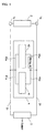
- FIG. 1 shows a power converter in accordance with a first embodiment of the present invention.
- the power converter shown includes a direct current power source 2 connected between input terminals 1 a ⁇ positive (+) ⁇ and 1 b ⁇ negative (-) ⁇ , a power module 3, which may include switching elements for the power such as IGBT (Insulated Gate Bipolar Transistor), connected to the direct current power source 2, and a smoothing condenser 4 connected to the power module 3 in parallel.
- the direct current power source 2, the power module 3 and the smoothing condenser 4 are shown connected to each other by a power line 31.
- the power module 3 may include, for example, a semiconductor switching element and controls to convert a direct current power supplied from the direct current power source 2 into an alternating current power and output.
- the power module 3 may be driven according to a carrier frequency "fc" in several kHz to execute a power converting operation. Further, the carrier frequency in the first embodiment may be set to be about 5 kHz.
- the smoothing condenser 4 may include a first smoothing condenser 41 and second smoothing condenser 42, which may be connected in parallel and may have different characteristics.
- Each of the first and second smoothing condensers may also be a set of the condensers, which may be connected in parallel or series and may have the same characteristics.
- first smoothing condenser 41 and the second smoothing condenser 42 are shown connected to the power line 31 by using a wiring 41 a of the first smoothing condenser 41 and a wiring 42a of the second smoothing condenser 42.
- the first smoothing condenser 41 may be arranged closer around the power module 3 compared to the second smoothing condenser 42.
- an aluminum electrolytic condenser used as the first smoothing condenser 41 may have a large electrostatic capacity per volume.
- the aluminum electrolytic condenser may be suitable in terms of reducing the volume of the condenser.
- An impedance of the aluminum electrolytic condenser tends to increase at high frequencies.
- a high frequency ripple current may be generated. Because it may be necessary to absorb the high frequency ripple current (which may include a high-order harmonic component), the aluminum electrolytic condenser with a large volume may be used at the high frequency area wherein a higher impedance is obtained.
- the volume of the smoothing condenser may increase so as to absorb the ripple current.
- a ceramic condenser used as the second smoothing condenser 42 may have an electrostatic capacity per volume smaller than the aluminum electrolytic condenser.
- the volume of the condenser may become greater.
- the electrostatic capacity per ceramic condenser is small, it may be appropriate to arrange a plurality of the ceramic condensers "in parallel" to obtain the desired electrostatic capacity. As a result, the wiring may become complicated and the volume related to the wiring may be increased.
- An impedance of the ceramic condenser in the high frequency range may be lower than the aluminum electrolytic condenser. Further, because the heat radiating performance of the ceramic condenser may also be superior, the ceramic condenser may be suitable for the inverter of performing high-speed switching. This is because the high frequency ripple current may be generated so that it (including a high-order harmonic component) is absorbed with low impedance to lessen heating.
- the volume per electrostatic capacity may be small, in case of using the ceramic condenser as a smoothing condenser for the high power and high speed switching inverter, the volume of the smoothing condenser may tend to increase to secure the electrostatic capacity corresponding to the high power inverter.
- the smoothing condenser only with the ceramic condenser it may be advantageous to connect about 20 to 100 ceramic condensers in parallel wherein the number of the ceramic condenser varies depending on the capacity of a single ceramic condenser, thereby causing deterioration in productivity.
- the volume of the condenser compared to constituting only with the aluminum electrolytic condenser, the volume may be reduced to 1/20.
- the advantages thereof are less.
- the first smoothing condenser 41 and the second smoothing condenser 42 may having different characteristics are connected in parallel.
- the electrostatic capacity corresponding to the high-power inverter may mainly be contained in the first smoothing condenser 41 (e.g., aluminum electrolytic condenser).
- the ripple current for corresponding to the high speed switching inverter may mainly be absorbed in the second smoothing condenser 42 (e.g., ceramic condenser).
- the aluminum electrolytic condenser which is the first smoothing condenser 41, does not require the capacity and volume to absorbing the high frequency ripple current, it may be prepared with a minimum electrostatic capacity required for corresponding to the high power inverter.
- the ceramic condenser which is the second smoothing condenser 42, may be prepared with a minimum electrostatic capacity for absorbing the ripple current and a multiple parallel connection thereof is not required.
- the volume of the condenser may be reduced to about 1/30 when the condenser comprises the first smoothing condenser 41 and the second smoothing condenser 42, which are connected in parallel and which may have different characteristics, compared to when the smoothing condenser comprises only the aluminum electrolytic condenser. Further, compared to the case of constituting the smoothing condenser with only the ceramic condenser, the number of parallel connections may be greatly reduced. Further, the volume may be reduced to about 3/5 of the original volume.
- the film condenser may be inferior in view of the ratio of electrostatic capacity to volume, but may have superior ripple current capability. Further, compared to the ceramic condenser, the film condenser may be superior in terms of the ratio of electrostatic capacity to volume, but may have inferior ripple current capability.
- the volume may be reduced as well. Also, in the case of constituting the first smoothing condenser 42 with the film condenser and the second smoothing condenser with the ceramic condenser, the volume may be reduced.
- the first smoothing condenser 41 and the second smoothing condenser 42 may have a different frequency characteristics of impedance from each other.
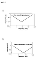
- the first smoothing condenser 41 may have the frequency characteristic depicted in Figure 2(a)
- the second smoothing condenser has the frequency characteristic depicted in Figure 2(b) .
- the first smoothing condenser 41 having such a frequency characteristic may comprise the aluminum electrolytic condenser, while the second smoothing condenser 42 may comprise the ceramic condenser.
- a magnitude relation of the electrostatic capacity between the first smoothing condenser 41 and the second smoothing condenser 42 may be set such that an electrostatic capacity C2 of the second smoothing condenser 42 is smaller than an electrostatic capacity C1 of the first smoothing condenser 41 (i.e., C1 > C2). This may result in lessening the volume of the smoothing condenser 4, as mentioned above.
- the volume advantage may easily be obtainable as an inevitable consequence when the capacity of the first smoothing condenser 41 is set to be larger.
- the inductance of the first smoothing condenser 41 and the second smoothing condenser 42 may be set as explained below.
- the equivalent serial inductance of the first smoothing condenser 41 is set as ESL1
- the equivalent serial inductance of the second smoothing condenser 42 may be set as ESL2
- the inductance of the wiring for connecting the power module 3 and the first smoothing condenser 41 is set as H1
- the inductance of the wiring for connecting the power module 3 and the second smoothing condenser 42 may be set at H2.
- the wiring inductance H2 of the second smoothing condenser 42 viewed from the power module 3 may be set to become greater than the wiring inductance H1 of the first smoothing condenser 41 (H1 ⁇ H2).
- the wiring inductance ⁇ L may be added.
- a method to add the wiring inductance ⁇ L to the wiring 42a of the second smoothing condenser 42 may include establishing a wiring length thereof to be longer than the wiring 41 a of the first smoothing condenser 41.
- a wiring length thereof may be longer than the wiring 41 a of the first smoothing condenser 41.
- a distance of the wiring 41 a of the first smoothing condenser 41 may be equidistant to a distance of the wiring 42a of the second smoothing condenser 42.
- the positive (+) side wiring connected to the input terminal 1a side ⁇ positive (+) side ⁇ and the negative (-) side wiring connected to the input terminal 1 b side ⁇ negative (-) side ⁇ of the direct current power source 2 may be arranged to overlap with each other such that the wiring inductance of the inductance related to the first smoothing condenser 41 becomes cancelled.
- the wiring 42a of the second smoothing condenser 42 may be arranged to be parallel without overlapping. That is, because a cancellation effect of the magnetic field may not be operated compared to the wiring 41 a of the first smoothing condenser 41, the wiring inductance may become greater.
- the wiring inductance ⁇ L may be added by appropriately adjusting the arrangement and length of the wiring to obtain H1 ⁇ H2.
- Figure 4 is a schematic view depicting frequency characteristics of the first smoothing condenser 41 and the second smoothing condenser (i.e., illustrating ideal characteristics).
- the impedance of the first smoothing condenser 1 may be decreased according to the electrostatic capacity as the frequency of the current increases. In the ideal characteristic, it may be reduced to "0" in such a state.
- the impedance may tend to increase as the frequency of the current increases. That is, at a particular frequency (magnetic resonance frequency), the impedance characteristic wherein the condenser component is dominant may be changed to the impedance characteristic wherein the inductance component is dominant.
- Such tendency may be the same as in the second smoothing condenser 42, although the characteristics thereof may differ from that of the first smoothing condenser 41.
- an area wherein the condenser component is dominant is indicated with a solid line, whereas an area wherein the inductance component is dominant is indicated with a dotted line.
- the following areas exist: a frequency area wherein the condenser component is dominant in the characteristics of both the first and second smoothing condensers (i.e., Area I: both condensers are indicated with the solid line); a frequency area wherein the condenser component and the inductance component are dominant in the characteristics of both the first and second smoothing condensers (i.e., Area II: both condensers are indicated with the solid line and the dotted line); and a frequency area wherein the inductance component is dominant in the characteristics of both the first and second smoothing condensers (i.e., Area III: both condensers are indicated with the dotted line).
- both condensers are either in a parallel connection with the condenser C or a parallel connection with the inductance L in Areas I and III
- the synthetic impedance of combining both condensers is indicated as a mere synthetic impedance.
- the impedance may become a parallel connection of the condenser C and the inductance L in Area II.
- the parallel connection of the condenser C and the inductance L may form a so-called "resonance" circuit.
- the synthetic impedance may be unlimited wherein there is no resistance of the direct current component.
- the resistance in the direct current component may be the same as ESR or the wiring resistance of the first smoothing condenser 41 or the second smoothing condenser 42, this synthetic impedance may be absorbed by such a resistance so that the synthetic impedance cannot be practically unlimited.
- the synthetic impedance may become greater than the frequency prior to or after the absorption.
- the impedance of the first smoothing condenser 41 when there is no inductance difference ⁇ L (H2 - H1) (prior to the adjustment as in the prior art), the impedance of the first smoothing condenser 41 may be set as Z1, the impedance of the second smoothing condenser 42 may be set as Z2, and the synthetic impedance of both condensers may be set as Z.
- the impedance of the first smoothing condenser 41 is set as Z1'
- the impedance of the second smoothing condenser 42 is set as Z2'
- the synthetic impedance of both condensers may be set as Z'.
- the synthetic impedance when there is no inductance difference (prior to the adjustment), the synthetic impedance may be increased by the resonance in an area corresponding to Area II as discussed above. When there is an inductance difference (after the adjustment), a peak value of the synthetic impedance may be decreased. This is because the resonance frequency of the first smoothing condenser 41 and the second smoothing condenser 42 may be close to each other by adding the inductance difference to the second smoothing condenser 42.
- the peak value of the synthetic impedance may be decreased as it is set that the impedance of both condensers may become lower at the frequency, which may become a parallel resonance frequency (i.e., impedance is unlimited). Because the impedance becomes unlimited at the parallel resonance frequency, the resonance may be attenuated by the direct current resistance component. However, the energy of the resonance may be attenuated by decreasing the amount of energy of generating the resonance as well.
- the energy of the resonance may be current based on the energy accumulated in the condenser component and inductance component, in order to lessen the amount of energy at the time of reaching the resonance, the impedance of the first and second smoothing condensers may be suppressed to be smaller at the parallel resonance frequency.
- each impedance of the first and second smoothing condensers may become a minimum at a serial resonance frequency (frequency at which the area wherein the condenser component is dominant is switched to the area wherein the inductance component is dominant).
- the area of the first and second smoothing condensers with low impedance inevitably may become the resonance area. That is, if the serial resonance frequencies of both condensers become closer, because the area of both condensers with the minimum impedance component becomes closer to the parallel resonance frequency, the impedance of the first and second smoothing condensers at the parallel resonance frequency may be decreased.
- the area wherein the inductance component is dominant may be broadened by adding the wiring inductance ⁇ L to the second smoothing condenser 42. This is so that the serial resonance frequency of the second smoothing condenser 42 may be decreased accordingly. In this regard, it may be possible to make the serial resonance frequency of the second smoothing condenser 42 to become closer to the serial resonance frequency of the first smoothing condenser 41.
- serial resonance frequency f1 of the first smoothing condenser 41 and the serial resonance frequency f2 of the second smoothing condenser 42 may be indicated as the following formulas.
- f ⁇ 1 1 / 2 ⁇ ⁇ ⁇ ( C ⁇ 1 ⁇ L ⁇ 1 ) 1 / 2
- f ⁇ 2 1 / 2 ⁇ ⁇ ⁇ ( C ⁇ 2 ⁇ L ⁇ 2 ) 1 / 2
- f3 1 / 2 ⁇ ⁇ ⁇ ( C ⁇ 1 ⁇ C ⁇ 2 ) 1 / 2 ⁇ / ⁇ L ⁇ 1 + L ⁇ 2 ⁇ C ⁇ 1 ⁇ C ⁇ 2 ⁇ 1 / 2
- each of the serial resonance frequencies f1 and f2 and the parallel resonance frequency f3 may depend on a value of multiplying the corresponding electrostatic capacities C1 and C2 and the inductance L1 and L2 of the smoothing condensers (C1 x L1, C2 x L2).
- the ripple current at the parallel resonance frequency may be reduced.
- the heating may be reduced to thereby achieve the miniaturization of the smoothing condenser 4.
- both the electrostatic capacity 22 and inductance L22 of the other smoothing condenser may be set to be smaller. This is because it may be intended to reduce the loss caused by the ripple current by decreasing the inductance L22 as much as possible so that the other smoothing condenser may absorb the ripple current.
- a multiplication of the electrostatic capacity and inductance of one smoothing condenser may be set to be much greater than a multiplication of the electrostatic capacity and inductance of the other smoothing condenser (C22 x L22), i.e., (C11 x L11 1 >> C22 x L22).
- the electrostatic capacity C1 of the first smoothing condenser 41 may be set to be greater than the electrostatic capacity C2 of the second smoothing condenser 42 (C1 > C2), whereas the wiring inductance H2 of the second smoothing condenser 42 may be set to be greater than the wiring inductance H1 of the first smoothing condenser 41 (H1 ⁇ H2).
- the difference ( ⁇ CL1122) in the prior art may be greater than the difference ( ⁇ CL12) in the first embodiment ( ⁇ CL1122 > ⁇ CL12 ).
- the difference between the serial resonance frequency f1 of the first smoothing condenser 41 and the serial resonance frequency f2 of the second smoothing condenser 42 in the first embodiment may become smaller than that in the prior art. This is so that the impedance at the parallel resonance frequency f3 may become smaller as well.
- the ripple current of the first smoothing condenser 41 may be reduced.
- ESL of the second smoothing condenser 42 may be lower than ESL of the first smoothing condenser 41, the magnetic resonance frequencies of both condensers may become closer by adding the wiring inductance ⁇ L.
- Figure 7 depicts a power converter in accordance with a second embodiment of the present invention.
- the impedance of the parallel resonance frequency of both condensers may be reduced by adding the wiring inductance ⁇ L to the second smoothing condenser 42 in the first embodiment.
- the impedance at the parallel resonance frequency of the first smoothing condenser 41 and the second smoothing condenser 42, which are connected in parallel is set to be smaller than the synthetic impedance at a carrier frequency of the power module 3.
- a wiring resistance ⁇ R to the wiring 42b of the second smoothing condenser 42 (i.e., in addition to the wiring inductance ⁇ L).
- a wiring resistance ⁇ R may increase the resistance of the wiring 42b compared to that of the first embodiment by adding the wiring resistance ⁇ R by increasing the wiring length of the wiring 42b of the second smoothing condenser 42 compared to the first embodiment or thinning the wiring width.
- Figure 9 depicts frequency characteristics of the impedance with regard to simulation results wherein each quantity of the first smoothing condenser 41 and the second smoothing condenser 42 is as follows. The following is an example wherein the operational current is the frequency characteristic per one ampere.
- Electrostatic capacity C1 of the first smoothing condenser 41 1000 ⁇ F ESL (ESL1) of the first smoothing condenser 41: 200 nH Equivalent serial resistance (ESR1) of the first smoothing condenser 41: 20 m ⁇
- Electrostatic capacity C2 of the second smoothing condenser 42 150 ⁇ F ESL (ESL2) of the second smoothing condenser 42: 20 nH Equivalent serial resistance (ESR2) of the second smoothing condenser 42: 2 m ⁇ Inductance difference ⁇ L (H2 - H1): 50 nH Wiring resistance difference ⁇ R (R2 - R1): 10 m ⁇
- each quantity may be the same as shown in Figure 5 .
- the frequency characteristic of the impedance Z1 (fc) of the first smoothing condenser 41 may become almost the same as the frequency characteristic of the synthetic impedance Z (fc) of the first smoothing condenser 41 and the second smoothing condenser 42, which may be connected in parallel.
- the serial resonance frequency f1 of the first smoothing condenser, the serial resonance frequency f2 of the second smoothing condenser 42 and the parallel resonance frequency f3 of the first smoothing condenser 41 and the second smoothing condenser 42 may be set as the frequency band equal to or more than 10 kHz, which is higher than the carrier frequency fc.
- a vicinity of the parallel resonance frequency f3 may be indicated by the high-order harmonic component of the carrier frequency fc and the so-called high frequency ripple current may be generated therein.
- the impedance Z1 of the first smoothing condenser 41, the impedance Z2 of the second smoothing condenser 42 and the synthetic impedance Z of the first smoothing condenser 41 and the second smoothing condenser 42 may be indicated as the following formulas.
- Z ⁇ 1 ⁇ ESR ⁇ 12 + ⁇ ESL ⁇ 1 - 1 / ⁇ / C ⁇ 1 ⁇ 2 ⁇ 1 / 2 ;
- Z ⁇ 2 ⁇ R ⁇ 22 + ⁇ L ⁇ 2 - 1 / ⁇ / C ⁇ 2 ⁇ 2 ⁇ 1 / 2 ;
- Z Z ⁇ 1 ⁇ Z ⁇ 2 / ( Z ⁇ 1 + Z ⁇ 2 )
- the impedance Z1 of the first smoothing condenser 41, the impedance Z2 of the second smoothing condenser 42 and the total of both impedances (Z1 + Z2) may be approximated as follows.
- the synthetic impedance Z (f3) at the parallel resonance frequency may be indicated as follows based on the above Formulas 3 and 4 by using such an approximation.
- the synthetic impedance Z (fc) at the carrier frequency fc may be approximated to the impedance Z1 (fc) of the first smoothing condenser 41 at the carrier frequency fc indicated as follows.
- Z fc ⁇ Z ⁇ 1 fc ⁇ 1 / ⁇ cC ⁇ 1 , where ⁇ c 2 ⁇ fc.
- the synthetic impedance at the parallel resonance frequency may be suppressed by establishing the electrostatic capacity C2 of the second smoothing condenser 42 to be smaller than the electrostatic capacity C1 of the first smoothing condenser 41 (C1 > C2), establishing R2 to be large so as to become the relationship in Formula 7, and establishing the synthetic impedance Z (f3) at the parallel resonance frequency to be smaller than the synthetic impedance Z (fc) at the carrier frequency fc of the power module.
- the synthetic impedance at the parallel resonance frequency may be suppressed by adding the inductance ⁇ L in the first embodiment, in order to further increase the effect of suppression (particularly to allow the voltage change at the parallel resonance frequency to be smaller than the voltage change at the carrier frequency of the power module 3), it may be effective to add the resistance ⁇ R as well as the inductance ⁇ L.
- the synthetic impedance at the parallel resonance frequency may be reduced compared to that of the first embodiment.
- the ripple current flowing in the first smoothing condenser 41 may be reduced, the ripple current flowing in the second smoothing condenser 42 at the higher frequency area may not be inferior to that in the first embodiment.
- the ripple current branched into the first smoothing condenser 41 at the high frequency area may be increased.
- the smoothing condenser 4 including the first smoothing condenser 41 and the second smoothing condenser 42, connected in parallel may be prepared as the condenser with a superior high frequency characteristic. Further, it may be possible to suppress a surge voltage, which may be easily generated in the first smoothing condenser 41 having large ESL. As such, it may be possible to adopt the lower pressure resistance condenser to the first smoothing condenser 41, thereby promoting the miniaturization.
- the wiring inductance at the second smoothing condenser 42 side when making the wiring inductance at the second smoothing condenser 42 side to be large, it may be possible to suppress the increase of synthetic impedance at the parallel resonance frequency by establishing the electrostatic capacity C1 of the first smoothing condenser 41 to be greater than the electrostatic capacity C2 of the second smoothing condenser 42 (C1 > C2) and adding the resistance ⁇ R, wherein the synthetic impedance Z (f3) at the parallel resonance frequency may be smaller than the synthetic impedance Z (fc) at the carrier frequency fc of the power module 3. Further, it may also be possible to reduce the electrostatic capacity without deteriorating the characteristic of the second smoothing condenser 42 at the high frequency area, thereby miniaturizing the constitution.
- Figure 11 depicts a power converter in accordance with a third embodiment of the present invention.
- the wiring inductance of the second smoothing condenser 42 may be greater than that of the first smoothing condenser 41 and the inductance difference therebetween may be ⁇ L in the first and second embodiments.
- the serial resistance component of the wiring at the second smoothing condenser 42 side may be greater than that at the first smoothing condenser 41 side and the resistance difference therebetween may be ⁇ R in the second embodiment.
- the wiring inductance at the second smoothing condenser 42 side may be greater than that at the first smoothing condenser 41 side and the inductance difference therebetween is ⁇ L.
- the serial resistance component of the first smoothing condenser 41 may be greater than that of the second smoothing condenser 42 and the resistance difference therebetween is ⁇ R.
- the impedance may be adjusted at the parallel resonance frequency by the relationship between the inductance difference ⁇ L and the resistance difference ⁇ R.
- the synthetic impedance at the parallel resonance frequency of the first smoothing condenser 41 and second smoothing condenser 42, in parallel may be set to be smaller than the synthetic impedance at the carrier frequency of the power module 3.
- Such a feature may be utilized by adding the serial resistance component ⁇ R to the wiring 41 a of the first smoothing condenser 41.
- the wiring length of the first smoothing condenser 41 may be set to be longer than the wiring length of the second smoothing condenser 42.
- the electrostatic capacity C1 of the first smoothing condenser 41 may be set to be greater than the electrostatic capacity C2 of the second smoothing condenser 42 (C1 > C2).
- the synthetic impedance Z (f3) at the parallel resonance frequency may be set to be smaller than the synthetic impedance Z (fc) at the carrier frequency of the power module 3.
- R11 is a value of adding the wiring resistance to ESR1 of the first smoothing condenser 41.
- the synthetic impedance Z (f3) at the parallel resonance frequency may be much smaller than the synthetic impedance Z (fc) at the carrier frequency of the power module 3 by the above relationship to thereby suppress the surge voltage.
- the voltage changes at both smoothing condensers may be approximately the same, it may be possible to suppress the voltage change difference caused by the wiring impedance difference.
- it becomes possible to adopt the low pressure resistance condenser it may be possible to miniaturize both the first smoothing condenser 41 and the second smoothing condenser 42.
- Figures 13 and 14 depict an example of the impedance (operational current per one ampere) at each smoothing condenser and the frequency characteristics of the ripple current.
- the frequency characteristics shown in Figures 13 and 14 indicate a result of simulation wherein each quantity is as follows.
- Electrostatic capacity C1 of the first smoothing condenser 41 1000 ⁇ F; ESL (ESL1) of the first smoothing condenser 41: 200 nH; Equivalent serial resistance (ESR1) of the first smoothing condenser 41: 20 m ⁇ ; Electrostatic capacity C2 of the second smoothing condenser 42: 150 ⁇ F; ESL (ESL2) of the second smoothing condenser 42: 20 nH; Equivalent serial resistance (ESR2) of the second smoothing condenser 42: 2 m ⁇ ; Inductance difference ⁇ L (H2 - H1): 50 nH; and Wiring resistance difference ⁇ R (R1 - R2): 10 m ⁇ .
- the resonance current flowing between the first smoothing condenser 41 and second smoothing condenser 42 may be suppressed by making the resonance frequencies of both smoothing condensers to be closer. Further, the total current of both condensers at the resonance frequency may be reduced. Because it may be possible to establish the synthetic impedance Z (f3) at the parallel resonance frequency to be much smaller than the synthetic impedance Z (fc) at the carrier frequency of the power module 3, the surge voltage may be suppressed.
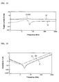
- Figures 15 and 16 depict the impedance and frequency characteristics of the ripple current of the fourth embodiment.
- the serial resonance frequency and parallel resonance frequency of the first smoothing condenser 41 and second smoothing condenser 42 may be allowed to be approximately the same in the fourth embodiment.
- the other features may be the same as in the first embodiment.
- the magnitude relation of the inductance between the first smoothing condenser 41 and the second smoothing condenser 42 may be the same as in the first embodiment. Further, the ratio of the electrostatic capacities of the first smoothing condenser and the second smoothing condenser (C1 : C2) may be changed. Also, the electrostatic capacity and inductance of each smoothing condenser and the inductance by the wiring may be adjusted and set such that the ratio of the electrostatic capacity and the ratio of the inductance (L1 : L2) may become a reciprocal ratio (C1 : C2 ⁇ L2 : L1).
- the multiplication of the electrostatic capacity C1 of the first smoothing condenser 41 and the inductance L1 (C1 x L1) and the multiplication of the electrostatic capacity C2 of the second smoothing condenser 42 and the inductance L2 (C2 x L2) may be set to be approximately the same with each other (C1 x L1 ⁇ C2 x L2).
- the serial resonance frequency f1 of the first smoothing condenser 41, the serial resonance frequency f2 of the second smoothing condenser 42 and the parallel resonance frequency f3 of the first smoothing condenser 41 and second smoothing condenser 42 may be approximately the same.
- the resonance current may be reduced to a very small value.
- Figure 15 depicts an example of the frequency characteristics of the impedance (operational current per one ampere) of each smoothing condenser when the first smoothing condenser 41 and the second smoothing condenser 42 are within the electrostatic capacity and inductance difference ⁇ L below.
- the frequency characteristics shown in Figure 15 indicate a result of simulation wherein each quantity is as follows.
- Electrostatic capacity C1 of the first smoothing condenser 41 650 ⁇ F ESL (ESL1) of the first smoothing condenser 41: 200 nH Equivalent serial resistance (ESR1) of the first smoothing condenser 41: 20 m ⁇
- Electrostatic capacity C2 of the second smoothing condenser 42 500 ⁇ F ESL (ESL2) of the second smoothing condenser 42: 20 nH Equivalent serial resistance (ESR2) of the second smoothing condenser 42: 2 m ⁇ Inductance difference ⁇ L (H2 - H1): 50 nH
- embodiments disclosed herein provide a power converter comprising smoothing condensers having high electrostatic capacity and ripple current withstand while promoting the miniaturization thereof.
- a power condenser comprising a power module having a plurality of switching elements and a smoothing condenser connected to the power module, wherein: the smoothing condenser includes a first smoothing condenser and a second smoothing condenser connected in parallel; a frequency characteristic of impedance of the first smoothing condenser is different from a frequency characteristic of impedance of the second smoothing condenser; an electrostatic capacity of the first smoothing condenser is greater than an electrostatic capacity of the second smoothing condenser; and an inductance of a wiring for connecting the second smoothing condenser and the power module is greater than an inductance of a wiring for connecting the first smoothing condenser and the power module.
- the resonance current between the first smoothing condenser and the second smoothing condenser may be reduced. Consequently, it may be possible to reduce the ripple current of the smoothing condenser to thereby miniaturize the smoothing condensers.
Landscapes
- Engineering & Computer Science (AREA)
- Power Engineering (AREA)
- Inverter Devices (AREA)
Applications Claiming Priority (3)
| Application Number | Priority Date | Filing Date | Title |
|---|---|---|---|
| JP2007178213 | 2007-07-06 | ||
| JP2007178216 | 2007-07-06 | ||
| JP2008160224A JP5338154B2 (ja) | 2007-07-06 | 2008-06-19 | 電力変換装置 |
Publications (3)
| Publication Number | Publication Date |
|---|---|
| EP2012418A2 true EP2012418A2 (de) | 2009-01-07 |
| EP2012418A3 EP2012418A3 (de) | 2012-08-29 |
| EP2012418B1 EP2012418B1 (de) | 2018-06-27 |
Family
ID=39817095
Family Applications (1)
| Application Number | Title | Priority Date | Filing Date |
|---|---|---|---|
| EP08159691.8A Active EP2012418B1 (de) | 2007-07-06 | 2008-07-04 | Stromwandler |
Country Status (2)
| Country | Link |
|---|---|
| US (1) | US8107269B2 (de) |
| EP (1) | EP2012418B1 (de) |
Families Citing this family (5)
| Publication number | Priority date | Publication date | Assignee | Title |
|---|---|---|---|---|
| JP5397410B2 (ja) | 2011-05-16 | 2014-01-22 | 株式会社デンソー | 車載用電気システム |
| US9800434B2 (en) * | 2013-04-22 | 2017-10-24 | International Business Machines Corporation | Millimeter wave phase shifters using tunable transmission lines |
| KR101452642B1 (ko) * | 2013-09-02 | 2014-10-22 | 엘에스산전 주식회사 | 역률 보상 회로 |
| US9893603B2 (en) | 2014-06-06 | 2018-02-13 | Hitachi Automotive Systems, Ltd. | Power converter |
| EP3240178B1 (de) | 2014-12-26 | 2020-05-06 | Nissan Motor Co., Ltd. | Stromwandlungsvorrichtung |
Citations (4)
| Publication number | Priority date | Publication date | Assignee | Title |
|---|---|---|---|---|
| JP2004254355A (ja) | 2003-02-18 | 2004-09-09 | Toshiba Corp | 電力変換装置 |
| JP2007178216A (ja) | 2005-12-27 | 2007-07-12 | Aisin Aw Co Ltd | 車両制御装置 |
| JP2007178213A (ja) | 2005-12-27 | 2007-07-12 | Yamato Scale Co Ltd | 軸重計測装置 |
| JP2008160224A (ja) | 2006-12-20 | 2008-07-10 | Sharp Corp | 電子機器システム |
Family Cites Families (7)
| Publication number | Priority date | Publication date | Assignee | Title |
|---|---|---|---|---|
| JPH0629149A (ja) * | 1992-07-10 | 1994-02-04 | Toshiba Corp | コンデンサ及びコンデンサユニット |
| US5414609A (en) * | 1992-08-25 | 1995-05-09 | Square D Company | DC to DC/DC to AC power conversion system |
| JPH11196570A (ja) | 1997-10-27 | 1999-07-21 | Fuji Electric Co Ltd | スイッチング電源等の平滑回路 |
| EP2113996A3 (de) * | 2001-09-25 | 2010-01-06 | Daikin Industries, Ltd. | Phasenstromerkennungsvorrichtung |
| JP4760097B2 (ja) * | 2005-03-31 | 2011-08-31 | 日本ケミコン株式会社 | キャパシタバンク用電極板及びキャパシタバンク |
| JP2007116861A (ja) * | 2005-10-24 | 2007-05-10 | Hitachi Industrial Equipment Systems Co Ltd | 電力変換装置 |
| JP4859443B2 (ja) * | 2005-11-17 | 2012-01-25 | 日立オートモティブシステムズ株式会社 | 電力変換装置 |
-
2008
- 2008-07-01 US US12/166,104 patent/US8107269B2/en active Active
- 2008-07-04 EP EP08159691.8A patent/EP2012418B1/de active Active
Patent Citations (4)
| Publication number | Priority date | Publication date | Assignee | Title |
|---|---|---|---|---|
| JP2004254355A (ja) | 2003-02-18 | 2004-09-09 | Toshiba Corp | 電力変換装置 |
| JP2007178216A (ja) | 2005-12-27 | 2007-07-12 | Aisin Aw Co Ltd | 車両制御装置 |
| JP2007178213A (ja) | 2005-12-27 | 2007-07-12 | Yamato Scale Co Ltd | 軸重計測装置 |
| JP2008160224A (ja) | 2006-12-20 | 2008-07-10 | Sharp Corp | 電子機器システム |
Also Published As
| Publication number | Publication date |
|---|---|
| US20090010029A1 (en) | 2009-01-08 |
| EP2012418B1 (de) | 2018-06-27 |
| US8107269B2 (en) | 2012-01-31 |
| EP2012418A3 (de) | 2012-08-29 |
Similar Documents
| Publication | Publication Date | Title |
|---|---|---|
| JP5338154B2 (ja) | 電力変換装置 | |
| US8614901B2 (en) | Inverter employing a boost chopper circuit and a resonant converter circuit | |
| US9166489B2 (en) | Layouts of multiple transformers and multiple rectifiers of interleaving converter | |
| CN102047550B (zh) | 电容器电路和电力变换电路 | |
| US7535133B2 (en) | Methods and apparatus for resistance compression networks | |
| US10224808B2 (en) | Electric power conversion device with snubber circuit | |
| EP2012418B1 (de) | Stromwandler | |
| US10498218B2 (en) | Switching circuit apparatus and electric power converter capable of reducing common mode noise in asymmetric circuit | |
| US10263505B2 (en) | Filtering of alternating voltage components in the intermediate circuit of a rectifier device of a motor vehicle | |
| CN104283448B (zh) | 电力变换装置 | |
| WO2018110071A1 (ja) | バスバ構造およびそれを用いた電力変換装置 | |
| CN105958828A (zh) | 一种dc-dc变换电路 | |
| CN102224669A (zh) | 具有多电平电压输出和谐波滤波器的功率转换器 | |
| Jacobs et al. | Multi-phase series resonant dc-to-dc converters: Stationary investigations | |
| JP4770083B2 (ja) | 電力変換装置 | |
| JP5387021B2 (ja) | フィルタ回路 | |
| JP2007236137A (ja) | ノイズフィルタ | |
| US20090302932A1 (en) | Feeding Arrangement for an Ultrasonic Device | |
| Inoue et al. | A novel filter built-in isolated bi-directional dc-dc converter with split windings | |
| JP2003143873A (ja) | 電力変換装置 | |
| JP4129817B2 (ja) | 電力変換回路 | |
| CN112636578B (zh) | Pfc电路及降噪电路 | |
| JP7802495B2 (ja) | 電力変換装置及びその製造方法 | |
| EP3629457B1 (de) | Leistungsmodul | |
| Kusui et al. | Theoretical Analysis and Experimental Validation of Current Balancing in Parallel MHz WPT Systems with a Coupled Inductor Pair |
Legal Events
| Date | Code | Title | Description |
|---|---|---|---|
| PUAI | Public reference made under article 153(3) epc to a published international application that has entered the european phase |
Free format text: ORIGINAL CODE: 0009012 |
|
| AK | Designated contracting states |
Kind code of ref document: A2 Designated state(s): AT BE BG CH CY CZ DE DK EE ES FI FR GB GR HR HU IE IS IT LI LT LU LV MC MT NL NO PL PT RO SE SI SK TR |
|
| AX | Request for extension of the european patent |
Extension state: AL BA MK RS |
|
| PUAL | Search report despatched |
Free format text: ORIGINAL CODE: 0009013 |
|
| AK | Designated contracting states |
Kind code of ref document: A3 Designated state(s): AT BE BG CH CY CZ DE DK EE ES FI FR GB GR HR HU IE IS IT LI LT LU LV MC MT NL NO PL PT RO SE SI SK TR |
|
| AX | Request for extension of the european patent |
Extension state: AL BA MK RS |
|
| RIC1 | Information provided on ipc code assigned before grant |
Ipc: H02M 7/00 20060101AFI20120720BHEP Ipc: H02M 1/14 20060101ALI20120720BHEP Ipc: H01G 4/38 20060101ALI20120720BHEP |
|
| 17P | Request for examination filed |
Effective date: 20121123 |
|
| AKX | Designation fees paid |
Designated state(s): DE FR GB |
|
| RBV | Designated contracting states (corrected) |
Designated state(s): DE FR GB |
|
| STAA | Information on the status of an ep patent application or granted ep patent |
Free format text: STATUS: EXAMINATION IS IN PROGRESS |
|
| 17Q | First examination report despatched |
Effective date: 20170208 |
|
| GRAP | Despatch of communication of intention to grant a patent |
Free format text: ORIGINAL CODE: EPIDOSNIGR1 |
|
| STAA | Information on the status of an ep patent application or granted ep patent |
Free format text: STATUS: GRANT OF PATENT IS INTENDED |
|
| INTG | Intention to grant announced |
Effective date: 20180312 |
|
| GRAJ | Information related to disapproval of communication of intention to grant by the applicant or resumption of examination proceedings by the epo deleted |
Free format text: ORIGINAL CODE: EPIDOSDIGR1 |
|
| STAA | Information on the status of an ep patent application or granted ep patent |
Free format text: STATUS: EXAMINATION IS IN PROGRESS |
|
| GRAP | Despatch of communication of intention to grant a patent |
Free format text: ORIGINAL CODE: EPIDOSNIGR1 |
|
| STAA | Information on the status of an ep patent application or granted ep patent |
Free format text: STATUS: GRANT OF PATENT IS INTENDED |
|
| GRAS | Grant fee paid |
Free format text: ORIGINAL CODE: EPIDOSNIGR3 |
|
| INTC | Intention to grant announced (deleted) | ||
| GRAA | (expected) grant |
Free format text: ORIGINAL CODE: 0009210 |
|
| STAA | Information on the status of an ep patent application or granted ep patent |
Free format text: STATUS: THE PATENT HAS BEEN GRANTED |
|
| INTG | Intention to grant announced |
Effective date: 20180508 |
|
| AK | Designated contracting states |
Kind code of ref document: B1 Designated state(s): DE FR GB |
|
| REG | Reference to a national code |
Ref country code: GB Ref legal event code: FG4D |
|
| REG | Reference to a national code |
Ref country code: DE Ref legal event code: R096 Ref document number: 602008055737 Country of ref document: DE |
|
| REG | Reference to a national code |
Ref country code: FR Ref legal event code: PLFP Year of fee payment: 11 |
|
| REG | Reference to a national code |
Ref country code: DE Ref legal event code: R097 Ref document number: 602008055737 Country of ref document: DE |
|
| PLBE | No opposition filed within time limit |
Free format text: ORIGINAL CODE: 0009261 |
|
| STAA | Information on the status of an ep patent application or granted ep patent |
Free format text: STATUS: NO OPPOSITION FILED WITHIN TIME LIMIT |
|
| 26N | No opposition filed |
Effective date: 20190328 |
|
| PGFP | Annual fee paid to national office [announced via postgrant information from national office to epo] |
Ref country code: GB Payment date: 20250619 Year of fee payment: 18 |
|
| PGFP | Annual fee paid to national office [announced via postgrant information from national office to epo] |
Ref country code: DE Payment date: 20250620 Year of fee payment: 18 |
|
| PGFP | Annual fee paid to national office [announced via postgrant information from national office to epo] |
Ref country code: FR Payment date: 20250820 Year of fee payment: 18 |