EP2012355A2 - Wärmeableitende Platte und Halbleitervorrichtung - Google Patents
Wärmeableitende Platte und Halbleitervorrichtung Download PDFInfo
- Publication number
- EP2012355A2 EP2012355A2 EP08252304A EP08252304A EP2012355A2 EP 2012355 A2 EP2012355 A2 EP 2012355A2 EP 08252304 A EP08252304 A EP 08252304A EP 08252304 A EP08252304 A EP 08252304A EP 2012355 A2 EP2012355 A2 EP 2012355A2
- Authority
- EP
- European Patent Office
- Prior art keywords
- heat dissipation
- dissipation plate
- layer
- lamination
- copper
- Prior art date
- Legal status (The legal status is an assumption and is not a legal conclusion. Google has not performed a legal analysis and makes no representation as to the accuracy of the status listed.)
- Withdrawn
Links
Images


Classifications
-
- H—ELECTRICITY
- H10—SEMICONDUCTOR DEVICES; ELECTRIC SOLID-STATE DEVICES NOT OTHERWISE PROVIDED FOR
- H10W—GENERIC PACKAGES, INTERCONNECTIONS, CONNECTORS OR OTHER CONSTRUCTIONAL DETAILS OF DEVICES COVERED BY CLASS H10
- H10W40/00—Arrangements for thermal protection or thermal control
-
- H—ELECTRICITY
- H10—SEMICONDUCTOR DEVICES; ELECTRIC SOLID-STATE DEVICES NOT OTHERWISE PROVIDED FOR
- H10W—GENERIC PACKAGES, INTERCONNECTIONS, CONNECTORS OR OTHER CONSTRUCTIONAL DETAILS OF DEVICES COVERED BY CLASS H10
- H10W40/00—Arrangements for thermal protection or thermal control
- H10W40/20—Arrangements for cooling
- H10W40/25—Arrangements for cooling characterised by their materials
- H10W40/258—Metallic materials
-
- H—ELECTRICITY
- H10—SEMICONDUCTOR DEVICES; ELECTRIC SOLID-STATE DEVICES NOT OTHERWISE PROVIDED FOR
- H10W—GENERIC PACKAGES, INTERCONNECTIONS, CONNECTORS OR OTHER CONSTRUCTIONAL DETAILS OF DEVICES COVERED BY CLASS H10
- H10W40/00—Arrangements for thermal protection or thermal control
- H10W40/20—Arrangements for cooling
- H10W40/25—Arrangements for cooling characterised by their materials
- H10W40/255—Arrangements for cooling characterised by their materials having a laminate or multilayered structure, e.g. direct bond copper [DBC] ceramic substrates
-
- Y—GENERAL TAGGING OF NEW TECHNOLOGICAL DEVELOPMENTS; GENERAL TAGGING OF CROSS-SECTIONAL TECHNOLOGIES SPANNING OVER SEVERAL SECTIONS OF THE IPC; TECHNICAL SUBJECTS COVERED BY FORMER USPC CROSS-REFERENCE ART COLLECTIONS [XRACs] AND DIGESTS
- Y10—TECHNICAL SUBJECTS COVERED BY FORMER USPC
- Y10T—TECHNICAL SUBJECTS COVERED BY FORMER US CLASSIFICATION
- Y10T156/00—Adhesive bonding and miscellaneous chemical manufacture
- Y10T156/10—Methods of surface bonding and/or assembly therefor
- Y10T156/1052—Methods of surface bonding and/or assembly therefor with cutting, punching, tearing or severing
- Y10T156/1056—Perforating lamina
- Y10T156/1057—Subsequent to assembly of laminae
Definitions
- This invention relates to a heat dissipation plate used for a semiconductor package which encompasses a semiconductor element, such as various kinds of LSIs and ICs, and a semiconductor device using the heat dissipation plate.
- a semiconductor element generates more heat as output power goes up.
- a heat dissipation plate used for a semiconductor packages has various kinds of structures.
- Japanese laid-open patent application No. 2001-144237 discloses a graphite sheet lamination heat conductor combined with thin metal plates and graphite sheets, which is excellent in thermal conductivity as compared with a metal material. And a graphite sheet lamination heat conductor is proposed to radiate heat from an electronic device.
- the above-mentioned graphite sheet lamination heat conductor can perform a high heat conduction characteristics.
- a bonding part with the ceramic substrate may be damaged by a heat deformation, since the thermal expansion coefficient of the graphite sheet lamination heat conductor differs from greatly that of the ceramic substrate.
- Japanese patent No. 3862737 discloses a material for a heat dissipation plate that brings the thermal expansion coefficient of the material close to that of a ceramic substrate, which constitutes a semiconductor element, by laminating copper layers and molybdenum layers alternately.
- a heat dissipation plate is provided with a lamination of copper layer, molybdenum layer and graphite layer and outer copper layers each provided a surface of the lamination.
- a semiconductor device includes a heat dissipation plate, a semiconductor element having semiconductor chip and substrate, a frame having open ends at opposite sides and outer connecting terminal, a cover attached to the other open end of the frame member and a wire connecting the semiconductor element and the outer connecting terminal.
- the heat dissipation plate includes a lamination of copper layer, molybdenum layer and graphite layer, and outer copper layers provided on both surfaces of the lamination.
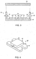
- Fig. 1 is a cross-sectional view illustrating a main portion of a heat dissipation plate for a semiconductor package according to a first embodiment.
- Fig. 2 is a plane view illustrating the plate shown in Fig. 1 .
- Fig. 3 is an exploded perspective view illustrating a semiconductor device according to a first embodiment.
- Fig. 4 is a perspective view including the semiconductor device shown in Fig. 3 .
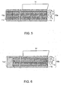
- Fig. 5 is a cross-sectional view illustrating a main portion of a heat dissipation plate according to a second embodiment.
- Fig. 6 is a cross-sectional view illustrating a main portion of a heat dissipation plate according to a third embodiment.
- Fig. 7 is a cross-sectional view illustrating a main portion of a heat dissipation plate according to a fourth embodiment.
- Fig. 8 is a cross-sectional view illustrating a main portion of a heat dissipation plate according to a fifth embodiment.
- Fig. 9 is a cross-sectional view illustrating a main portion of a heat dissipation plate according to a sixth embodiment.
- Fig. 10 is a cross-sectional view illustrating a main portion of a heat dissipation plate according to a seventh embodiment.
- a heat dissipation plate for a semiconductor package includes a lamination of a copper layer and a graphite layer, and outer copper layers, each of the outer copper layers provided to both sides of the lamination.
- Figs. 1 and 2 show a heat dissipation plate for a semiconductor device according to the first embodiment.
- Fig. 1 shows heat dissipation plate 10 on which semiconductor element 14 is mounted.
- Heat dissipation plate 10 has a flat plate structure having outer copper layers 11a, 11b at its both sides. Between outer copper layers 11a, 11b, for example, two sets of six layers of graphite layer 12, molybdenum layer 13, graphite layer 12, copper layer 11c, graphite layer 12 and copper layer 11c laminated in order, are laminated and further graphite layer 12, molybdenum 13 and graphite layer 12 are laminated in order on copper layer 12 of the second set of six layers.
- the graphite layer is excellent in thermal conductivity in a plane direction
- the copper layer is excellent in thermal conductivity in a direction vertical to a plane. That is, plural copper layers 11c, graphite layers 12, and molybdenum layers 13 are laminated alternately, and outer copper layers 11a, 11b are formed on both sides 16a and 16b of the lamination.
- Heat dissipation plate 10 has frame member 15, which is formed by laminating metal, for example, copper layer 11d and molybdenum layer 13a, at a periphery of the lamination, and each edge of graphite layer 12 is covered by frame member 15.
- Copper layers 11c, graphite layers 12, molybdenum layers 13 and outer copper layers 11a, 11b are stacked in order as mentioned above, and are subjected to pressure and heating process, and, for example, copper layer of 0.1 mm, graphite layer of 0.1 mm, molybdenum layer of 0.02mm and outer copper layers 11a and 11b of 0.2mm are laminated and integrated.
- An amount of molybdenum layers 13 is selected so that the thermal expansion coefficient of heat dissipation plate 10 becomes close to that of the ceramic substrate which constitutes the semiconductor element 14 mounted on heat dissipation plate 10.
- a ratio of a total thickness of outer copper layers 11a, 11b and copper layers 11c to a total thickness of graphite layers 12 is set as about 1.
- copper layers 11d and molybdenum layers 13a are stacked at the periphery of the lamination and between outer copper layers 11a, 11b, and are subjected to pressure and heating process, thereby copper layers 11d and molybdenum layers 13a are laminated and frame member 15 is thus formed.
- Frame member 15 is simultaneously formed, when the lamination and outer copper layers are integrated.
- the semiconductor device includes a heat dissipation plate having a lamination of copper layer, graphite layer and molybdenum layer, and outer copper layers provided on both surface of the lamination and a semiconductor element mounted on the heat dissipation pate.
- the semiconductor element includes semiconductor chip and substrate.
- the semiconductor device further includes a frame having open ends at opposite sides and outer connecting terminal. The frame member is attached to the heat dissipation plate and encompasses the semiconductor element. And a cover attached to the other open end of the frame member. And a wire connects the semiconductor element and the outer connecting terminal.
- Semiconductor device 20 shown in Figs. 3 and 4 is manufactured by preparing a treatment layer (not shown Figs. 1 and 2 ) such as a gold plating, on an outer surfaces of outer copper layers 11a, 11b, and frame member 15 of heat dissipation plate 10 shown in Fig. 1 and Fig. 2 , and mounting semiconductor element 14 on the treatment layer.
- a treatment layer such as a gold plating
- frame 21 which constitutes the semiconductor package is attached on one of outer copper layers (not shown) of heat dissipation plate 10.
- Outer connection terminals 22 pass through frame 21.
- ceramic substrate 141 and semiconductor chip 142 of semiconductor element 14 are mounted and bonded by using solder etc.
- Ceramic substrate 141 and semiconductor chip 142 are electrically connected with mutual and outer connection terminals 22 by conductive wires 24.
- Cover 23 which constitutes a semiconductor package is attached to the open end of frame 21, and thus semiconductor device 20 shown in Fig. 4 is formed.
- the thermal expansion coefficient of heat dissipation plate 10 is brought close to that of ceramic substrate 141 of semiconductor element 14 by the function of molybdenum layers 13.
- ceramic substrate 141 is bonded to heat dissipation plate 10 using solder etc., even if there is a temperature change caused by heating and cooling a bonding portion, highly precise bonding is maintained without braking ceramic substrate 141, since the thermal expansion coefficient of heat dissipation plate is brought close to that of ceramic substrate 141 and thermal deformations of heat dissipation plate 10 and ceramic substrate 141 become similar. In a same function, even if there is a temperature change of the package of semiconductor device 20, highly precise bonding is maintained without breaking the ceramic substrate 141 of a semiconductor device 14.
- heat dissipation plate 10 operates and generates heat, first the heat will be transferred to outer copper layer 11a and then the heat will be transferred to ceramic substrate 141 via outer copper layer 11a.
- thermal expansion coefficient of heat dissipation plate 10 is brought close to that of ceramic substrate 141 and heat deformations of heat dissipation plate 10 and ceramic substrate 141 are similar, highly precise bonding is maintained without braking ceramic substrate 141.
- the heat transferred to heat dissipation plate 10 is efficiently conducted in a direction vertical to a plate surface by outer copper layers 11a, 11b, copper layers 11c and frame member 15, and the heat is efficiently conducted in plane surface direction by graphite layer 12, and thereby the heat is conducted uniformly to whole the heat dissipation plate 10. Accordingly, semiconductor element 14 on heat dissipation plate 10 is efficiently heat-controlled while keeping a high precise mounting between outer copper layer 11a and semiconductor element 14.
- This invention is not limited to above-mentioned embodiment, it is possible to constitute heat dissipation plates for semiconductor packages 10a, 10b, 10c, 10d, 10e, and 10f as shown in, for example, Figs. 5, 6 , 7, 8 , 9 and 10 , and the similar effective effect are obtained. Moreover, semiconductor devices can be manufactured using these heat dissipation plates.
- the same numerals denote the same portions illustrated in Figs. 1 through 4 , and detailed explanations of those elements are omitted.
- Fig. 5 shows a heat dissipation plate for a semiconductor package according to the second embodiment.
- frame member 15a provided at a periphery is formed by laminating copper layers 11e, and other portion is formed by laminating outer copper layers 11a, 11b, copper layers 11c, graphite layers 12 and molybdenum layers 13 alternately as well as the embodiment shown in Fig. 1 .
- Fig. 6 shows a heat dissipation plate for a semiconductor package according to the third embodiment.
- frame member 15b provided at a periphery is formed of cupper, and frame member 15b and outer copper layer 11b are formed integrally.
- Fig. 7 shows a heat dissipation plate for semiconductor package according to the fourth embodiment.
- Heat dissipation plate 10c has semiconductor chip mounting portion 101a between outer copper layers 11a, 11b corresponding to area 101 which semiconductor chip 142 is mounted on, and semiconductor chip mounting portion 101a is formed by laminating copper layers 11c and molybdenum layers 13 without graphite layer 12.
- semiconductor chip mounting portion 101a the heat conductive ability in a direction vertical to a plane surface is improved by copper layer 11c and molybdenum layer 13 and a still better thermal conductivity is obtained.
- the heat from semiconductor chip 142 which heating value is concentrated in a semiconductor element, becomes possible to transfer more efficiently in the direction vertical to the plane surface.
- Fig. 8 shows a heat dissipation plate for a semiconductor package according to the fifth embodiment.
- semiconductor chip mounting portion 101b is formed by laminating copper layers 11c only without graphite layer 12 and molybdenum layer 13.
- semiconductor chip mounting portion 101b a heat conductive ability in a direction vertical to the plane surface is improved. Thereby the heat from semiconductor chip 142, which heating value is concentrated in a semiconductor element 14, becomes possible to transfer more efficiently in the direction vertical to the plane surface.
- Fig. 9 shows a heat dissipation plate for a semiconductor package according to the sixth embodiment.
- frame member 15b provided at the periphery is formed of copper only
- semiconductor chip mounting portion 101c is also formed of copper only.
- Frame member 15b, semiconductor chip mounting portion 101c and outer copper layer 11b are formed integrally.
- semiconductor chip 142 is mounted on heat dissipation plate 10e as heat dissipation plate 10d shown in Fig. 8
- Fig. 10 shows a heat dissipation plate for a semiconductor package according to the seventh embodiment.
- the first embodiment shown in Fig. 1 has frame member 15, heat dissipation plate 10f according to this embodiment does not have frame member 15.
- each molybdenum layer 13 is sandwiched by graphite layers 12 are explained.
- the invention is not limited to those embodiments, and molybdenum layer 13 may be inserted between graphite layer 12 and copper layer 11c, between outer copper layer 11a (11b) and copper layer 11c, or between copper layers 11c.
Landscapes
- Cooling Or The Like Of Semiconductors Or Solid State Devices (AREA)
Applications Claiming Priority (1)
| Application Number | Priority Date | Filing Date | Title |
|---|---|---|---|
| JP2007177636A JP4558012B2 (ja) | 2007-07-05 | 2007-07-05 | 半導体パッケージ用放熱プレート及び半導体装置 |
Publications (2)
| Publication Number | Publication Date |
|---|---|
| EP2012355A2 true EP2012355A2 (de) | 2009-01-07 |
| EP2012355A3 EP2012355A3 (de) | 2009-09-30 |
Family
ID=39765063
Family Applications (1)
| Application Number | Title | Priority Date | Filing Date |
|---|---|---|---|
| EP08252304A Withdrawn EP2012355A3 (de) | 2007-07-05 | 2008-07-04 | Wärmeableitende Platte und Halbleitervorrichtung |
Country Status (5)
| Country | Link |
|---|---|
| US (1) | US7745928B2 (de) |
| EP (1) | EP2012355A3 (de) |
| JP (1) | JP4558012B2 (de) |
| KR (1) | KR101015294B1 (de) |
| TW (1) | TWI438877B (de) |
Cited By (4)
| Publication number | Priority date | Publication date | Assignee | Title |
|---|---|---|---|---|
| US8034451B2 (en) | 2005-12-02 | 2011-10-11 | Morganite Electrical Carbon Limited | Carbon materials |
| WO2012139935A1 (de) * | 2011-04-12 | 2012-10-18 | BSH Bosch und Siemens Hausgeräte GmbH | Kühlvorrichtung für ein elektronikmodul eines haushaltsgeräts sowie baugruppe und haushaltsgerät mit einer kühlvorrichtung |
| WO2015055899A1 (fr) * | 2013-10-18 | 2015-04-23 | Griset | Support pour composants électroniques de puissance, module de puissance doté d'un tel support, et procédé de fabrication correspondant |
| EP3007531A4 (de) * | 2013-12-27 | 2016-08-31 | Huawei Tech Co Ltd | Wärmeleitendes verbundmaterialblech und herstellungsverfahren dafür |
Families Citing this family (17)
| Publication number | Priority date | Publication date | Assignee | Title |
|---|---|---|---|---|
| CN101496165B (zh) * | 2006-07-28 | 2011-01-19 | 京瓷株式会社 | 电子部件收容用封装件以及电子装置 |
| JP5105801B2 (ja) | 2006-09-05 | 2012-12-26 | 株式会社東芝 | 半導体装置 |
| JP5112101B2 (ja) * | 2007-02-15 | 2013-01-09 | 株式会社東芝 | 半導体パッケージ |
| US20100091477A1 (en) * | 2008-10-14 | 2010-04-15 | Kabushiki Kaisha Toshiba | Package, and fabrication method for the package |
| JP4643703B2 (ja) * | 2008-11-21 | 2011-03-02 | 株式会社東芝 | 半導体装置の固定具及びその取付構造 |
| JP2010192701A (ja) * | 2009-02-18 | 2010-09-02 | Showa Denko Kk | 発光ダイオード、発光ダイオードランプ及び発光ダイオードの製造方法 |
| JP5806464B2 (ja) * | 2010-02-03 | 2015-11-10 | 株式会社東芝 | 半導体素子収納用パッケージ及びそれを用いた半導体装置 |
| JP5450313B2 (ja) | 2010-08-06 | 2014-03-26 | 株式会社東芝 | 高周波半導体用パッケージおよびその作製方法 |
| US10988630B2 (en) | 2014-12-19 | 2021-04-27 | Certainteed Corporation | Coating compositions for building materials and coated building material substrates |
| US10108017B2 (en) | 2015-01-20 | 2018-10-23 | Microsoft Technology Licensing, Llc | Carbon nanoparticle infused optical mount |
| US10444515B2 (en) | 2015-01-20 | 2019-10-15 | Microsoft Technology Licensing, Llc | Convective optical mount structure |
| US9791704B2 (en) * | 2015-01-20 | 2017-10-17 | Microsoft Technology Licensing, Llc | Bonded multi-layer graphite heat pipe |
| US10028418B2 (en) | 2015-01-20 | 2018-07-17 | Microsoft Technology Licensing, Llc | Metal encased graphite layer heat pipe |
| KR102293885B1 (ko) * | 2015-02-03 | 2021-08-26 | 삼성디스플레이 주식회사 | 표시장치 |
| AU2017361096B2 (en) * | 2016-11-16 | 2022-09-01 | Magic Leap, Inc. | Thermal management systems for wearable components |
| EP3726572B1 (de) * | 2019-04-16 | 2025-08-13 | ABB Schweiz AG | Kühlkörperanordnung, verfahren zur herstellung einer kühlkörperanordnung und elektrische vorrichtung |
| WO2022250382A1 (ko) * | 2021-05-27 | 2022-12-01 | 주식회사 아모그린텍 | 히트싱크 일체형 세라믹 기판 및 그 제조방법 |
Citations (3)
| Publication number | Priority date | Publication date | Assignee | Title |
|---|---|---|---|---|
| JP2001144237A (ja) | 1999-11-18 | 2001-05-25 | Matsushita Electric Ind Co Ltd | グラファイトシート積層熱伝導体 |
| JP3862737B1 (ja) | 2005-10-18 | 2006-12-27 | 栄樹 津島 | クラッド材およびその製造方法、クラッド材の成型方法、クラッド材を用いた放熱基板 |
| JP2007177636A (ja) | 2005-12-27 | 2007-07-12 | Toyota Motor Corp | 燃料残量計および残走行距離計の制御システム |
Family Cites Families (20)
| Publication number | Priority date | Publication date | Assignee | Title |
|---|---|---|---|---|
| US346421A (en) * | 1886-07-27 | Brush | ||
| US328514A (en) * | 1885-10-20 | spbague | ||
| US349615A (en) * | 1886-09-21 | Signor to george westing house | ||
| US4689110A (en) * | 1983-12-22 | 1987-08-25 | Trw Inc. | Method of fabricating multilayer printed circuit board structure |
| US5224017A (en) | 1989-05-17 | 1993-06-29 | The Charles Stark Draper Laboratory, Inc. | Composite heat transfer device |
| US4963414A (en) | 1989-06-12 | 1990-10-16 | General Electric Company | Low thermal expansion, heat sinking substrate for electronic surface mount applications |
| US5276423A (en) * | 1991-11-12 | 1994-01-04 | Texas Instruments Incorporated | Circuit units, substrates therefor and method of making |
| US5156923A (en) | 1992-01-06 | 1992-10-20 | Texas Instruments Incorporated | Heat-transferring circuit substrate with limited thermal expansion and method for making |
| US5306571A (en) | 1992-03-06 | 1994-04-26 | Bp Chemicals Inc., Advanced Materials Division | Metal-matrix-composite |
| DE19605302A1 (de) | 1996-02-14 | 1997-08-21 | Fraunhofer Ges Forschung | Kühlkörper mit einer Montagefläche für ein elektronisches Bauteil |
| JP4272329B2 (ja) | 2000-03-15 | 2009-06-03 | 京セラ株式会社 | 半導体素子収納用パッケージ |
| JP2001313345A (ja) * | 2000-04-28 | 2001-11-09 | Kyocera Corp | 半導体素子収納用パッケージ |
| US6724079B2 (en) * | 2002-01-04 | 2004-04-20 | Motorola, Inc. | Wire bond-less electronic component for use with an external circuit and method of manufacture |
| JP2006013420A (ja) * | 2004-01-28 | 2006-01-12 | Kyocera Corp | 電子部品収納用パッケージおよび電子装置 |
| JP2005277382A (ja) * | 2004-02-23 | 2005-10-06 | Kyocera Corp | 電子部品収納用パッケージおよび電子装置 |
| JP4382547B2 (ja) * | 2004-03-24 | 2009-12-16 | 株式会社アライドマテリアル | 半導体装置用基板と半導体装置 |
| JP4711165B2 (ja) * | 2004-06-21 | 2011-06-29 | 日立金属株式会社 | 高熱伝導・低熱膨脹複合体およびその製造方法 |
| JP4575147B2 (ja) | 2004-12-28 | 2010-11-04 | 株式会社東芝 | 半導体装置 |
| JP4610414B2 (ja) | 2005-03-22 | 2011-01-12 | 京セラ株式会社 | 電子部品収納用パッケージおよび電子装置ならびに電子装置の実装構造 |
| JP5105801B2 (ja) | 2006-09-05 | 2012-12-26 | 株式会社東芝 | 半導体装置 |
-
2007
- 2007-07-05 JP JP2007177636A patent/JP4558012B2/ja not_active Expired - Fee Related
-
2008
- 2008-06-30 US US12/164,396 patent/US7745928B2/en not_active Expired - Fee Related
- 2008-07-01 TW TW097124724A patent/TWI438877B/zh not_active IP Right Cessation
- 2008-07-04 EP EP08252304A patent/EP2012355A3/de not_active Withdrawn
- 2008-07-04 KR KR1020080064762A patent/KR101015294B1/ko not_active Expired - Fee Related
Patent Citations (3)
| Publication number | Priority date | Publication date | Assignee | Title |
|---|---|---|---|---|
| JP2001144237A (ja) | 1999-11-18 | 2001-05-25 | Matsushita Electric Ind Co Ltd | グラファイトシート積層熱伝導体 |
| JP3862737B1 (ja) | 2005-10-18 | 2006-12-27 | 栄樹 津島 | クラッド材およびその製造方法、クラッド材の成型方法、クラッド材を用いた放熱基板 |
| JP2007177636A (ja) | 2005-12-27 | 2007-07-12 | Toyota Motor Corp | 燃料残量計および残走行距離計の制御システム |
Cited By (4)
| Publication number | Priority date | Publication date | Assignee | Title |
|---|---|---|---|---|
| US8034451B2 (en) | 2005-12-02 | 2011-10-11 | Morganite Electrical Carbon Limited | Carbon materials |
| WO2012139935A1 (de) * | 2011-04-12 | 2012-10-18 | BSH Bosch und Siemens Hausgeräte GmbH | Kühlvorrichtung für ein elektronikmodul eines haushaltsgeräts sowie baugruppe und haushaltsgerät mit einer kühlvorrichtung |
| WO2015055899A1 (fr) * | 2013-10-18 | 2015-04-23 | Griset | Support pour composants électroniques de puissance, module de puissance doté d'un tel support, et procédé de fabrication correspondant |
| EP3007531A4 (de) * | 2013-12-27 | 2016-08-31 | Huawei Tech Co Ltd | Wärmeleitendes verbundmaterialblech und herstellungsverfahren dafür |
Also Published As
| Publication number | Publication date |
|---|---|
| TWI438877B (zh) | 2014-05-21 |
| JP2009016621A (ja) | 2009-01-22 |
| KR20090004738A (ko) | 2009-01-12 |
| EP2012355A3 (de) | 2009-09-30 |
| KR101015294B1 (ko) | 2011-02-15 |
| US20090008770A1 (en) | 2009-01-08 |
| US7745928B2 (en) | 2010-06-29 |
| JP4558012B2 (ja) | 2010-10-06 |
| TW200917435A (en) | 2009-04-16 |
Similar Documents
| Publication | Publication Date | Title |
|---|---|---|
| EP2012355A2 (de) | Wärmeableitende Platte und Halbleitervorrichtung | |
| US8391011B2 (en) | Cooling device | |
| CN100517696C (zh) | 具有半导体元件、绝缘基板和金属电极的半导体器件 | |
| CN104603933B (zh) | 功率模块用基板及功率模块 | |
| US7361985B2 (en) | Thermally enhanced molded package for semiconductors | |
| US11075331B2 (en) | Thermoelectric device having circuitry with structural rigidity | |
| EP2237336A1 (de) | Thermoelektrische einrichtung | |
| KR101017452B1 (ko) | 반도체 패키지 | |
| WO2008013279A1 (en) | Electronic component storing package and electronic device | |
| TW200921871A (en) | Heat conductor | |
| JP2004022973A (ja) | セラミック回路基板および半導体モジュール | |
| JP4935220B2 (ja) | パワーモジュール装置 | |
| WO2019163941A1 (ja) | パワーモジュール用基板およびパワーモジュール | |
| CN120356878A (zh) | 夹子 | |
| JP3669980B2 (ja) | モジュール構造体の製造方法並びに回路基板の固定方法及び回路基板 | |
| US20140091444A1 (en) | Semiconductor unit and method for manufacturing the same | |
| JP6060053B2 (ja) | パワー半導体装置 | |
| WO2021085006A1 (ja) | パワー半導体装置およびパワー半導体装置の製造方法 | |
| JP4876612B2 (ja) | 絶縁伝熱構造体及びパワーモジュール用基板 | |
| KR20250147449A (ko) | 냉각효율을 향상시킨 반도체 장비용 히트싱크 | |
| JP2004096035A (ja) | モジュール構造体の製造方法並びに回路基板の固定方法及び回路基板 | |
| JP6406547B2 (ja) | 電子部品搭載用パッケージおよび電子装置ならびに電子モジュール | |
| WO2025023251A1 (ja) | 放熱部材 | |
| WO2016079970A1 (ja) | 冷却モジュール | |
| WO2023171019A1 (ja) | ヒートシンク一体型絶縁回路基板、および、電子デバイス |
Legal Events
| Date | Code | Title | Description |
|---|---|---|---|
| PUAI | Public reference made under article 153(3) epc to a published international application that has entered the european phase |
Free format text: ORIGINAL CODE: 0009012 |
|
| 17P | Request for examination filed |
Effective date: 20080710 |
|
| AK | Designated contracting states |
Kind code of ref document: A2 Designated state(s): AT BE BG CH CY CZ DE DK EE ES FI FR GB GR HR HU IE IS IT LI LT LU LV MC MT NL NO PL PT RO SE SI SK TR |
|
| AX | Request for extension of the european patent |
Extension state: AL BA MK RS |
|
| PUAL | Search report despatched |
Free format text: ORIGINAL CODE: 0009013 |
|
| AK | Designated contracting states |
Kind code of ref document: A3 Designated state(s): AT BE BG CH CY CZ DE DK EE ES FI FR GB GR HR HU IE IS IT LI LT LU LV MC MT NL NO PL PT RO SE SI SK TR |
|
| AX | Request for extension of the european patent |
Extension state: AL BA MK RS |
|
| 17Q | First examination report despatched |
Effective date: 20100420 |
|
| AKX | Designation fees paid |
Designated state(s): DE FR GB |
|
| GRAP | Despatch of communication of intention to grant a patent |
Free format text: ORIGINAL CODE: EPIDOSNIGR1 |
|
| STAA | Information on the status of an ep patent application or granted ep patent |
Free format text: STATUS: GRANT OF PATENT IS INTENDED |
|
| INTG | Intention to grant announced |
Effective date: 20180921 |
|
| STAA | Information on the status of an ep patent application or granted ep patent |
Free format text: STATUS: THE APPLICATION IS DEEMED TO BE WITHDRAWN |
|
| 18D | Application deemed to be withdrawn |
Effective date: 20190202 |