EP2012154A1 - Dispositif optique et procede de fabrication dudit dispositif optique - Google Patents
Dispositif optique et procede de fabrication dudit dispositif optique Download PDFInfo
- Publication number
- EP2012154A1 EP2012154A1 EP07740217A EP07740217A EP2012154A1 EP 2012154 A1 EP2012154 A1 EP 2012154A1 EP 07740217 A EP07740217 A EP 07740217A EP 07740217 A EP07740217 A EP 07740217A EP 2012154 A1 EP2012154 A1 EP 2012154A1
- Authority
- EP
- European Patent Office
- Prior art keywords
- optical
- light
- optical waveguide
- smoothing film
- waveguide cable
- Prior art date
- Legal status (The legal status is an assumption and is not a legal conclusion. Google has not performed a legal analysis and makes no representation as to the accuracy of the status listed.)
- Withdrawn
Links
- 230000003287 optical effect Effects 0.000 title claims abstract description 218
- 238000004519 manufacturing process Methods 0.000 title claims description 16
- 238000009499 grossing Methods 0.000 claims abstract description 86
- 238000005253 cladding Methods 0.000 claims abstract description 36
- 239000000463 material Substances 0.000 claims description 24
- 238000000034 method Methods 0.000 claims description 15
- 239000011344 liquid material Substances 0.000 claims description 9
- 230000008569 process Effects 0.000 claims description 7
- 239000011248 coating agent Substances 0.000 claims description 5
- 238000000576 coating method Methods 0.000 claims description 5
- 239000007921 spray Substances 0.000 claims description 5
- 239000012792 core layer Substances 0.000 abstract description 58
- 239000010410 layer Substances 0.000 abstract description 34
- 230000005540 biological transmission Effects 0.000 description 30
- 238000006243 chemical reaction Methods 0.000 description 16
- 239000013307 optical fiber Substances 0.000 description 10
- 239000011347 resin Substances 0.000 description 10
- 229920005989 resin Polymers 0.000 description 10
- 238000001878 scanning electron micrograph Methods 0.000 description 9
- 239000000758 substrate Substances 0.000 description 5
- 239000010931 gold Substances 0.000 description 4
- 238000005259 measurement Methods 0.000 description 4
- 229920001721 polyimide Polymers 0.000 description 4
- 238000004528 spin coating Methods 0.000 description 4
- BQCADISMDOOEFD-UHFFFAOYSA-N Silver Chemical compound [Ag] BQCADISMDOOEFD-UHFFFAOYSA-N 0.000 description 3
- 229910052782 aluminium Inorganic materials 0.000 description 3
- XAGFODPZIPBFFR-UHFFFAOYSA-N aluminium Chemical compound [Al] XAGFODPZIPBFFR-UHFFFAOYSA-N 0.000 description 3
- 238000004891 communication Methods 0.000 description 3
- PCHJSUWPFVWCPO-UHFFFAOYSA-N gold Chemical compound [Au] PCHJSUWPFVWCPO-UHFFFAOYSA-N 0.000 description 3
- 229910052737 gold Inorganic materials 0.000 description 3
- 230000000644 propagated effect Effects 0.000 description 3
- 230000009467 reduction Effects 0.000 description 3
- 229910052709 silver Inorganic materials 0.000 description 3
- 239000004332 silver Substances 0.000 description 3
- 230000003746 surface roughness Effects 0.000 description 3
- 239000004642 Polyimide Substances 0.000 description 2
- 238000005520 cutting process Methods 0.000 description 2
- 239000000428 dust Substances 0.000 description 2
- 239000003822 epoxy resin Substances 0.000 description 2
- 229910052751 metal Inorganic materials 0.000 description 2
- 239000002184 metal Substances 0.000 description 2
- 238000005498 polishing Methods 0.000 description 2
- 229920000548 poly(silane) polymer Polymers 0.000 description 2
- 229920000647 polyepoxide Polymers 0.000 description 2
- 229920000139 polyethylene terephthalate Polymers 0.000 description 2
- 239000005020 polyethylene terephthalate Substances 0.000 description 2
- 239000009719 polyimide resin Substances 0.000 description 2
- 229920000642 polymer Polymers 0.000 description 2
- 238000011144 upstream manufacturing Methods 0.000 description 2
- 239000004925 Acrylic resin Substances 0.000 description 1
- KRHYYFGTRYWZRS-UHFFFAOYSA-M Fluoride anion Chemical compound [F-] KRHYYFGTRYWZRS-UHFFFAOYSA-M 0.000 description 1
- XUIMIQQOPSSXEZ-UHFFFAOYSA-N Silicon Chemical compound [Si] XUIMIQQOPSSXEZ-UHFFFAOYSA-N 0.000 description 1
- 238000000089 atomic force micrograph Methods 0.000 description 1
- 239000004020 conductor Substances 0.000 description 1
- 230000008878 coupling Effects 0.000 description 1
- 238000010168 coupling process Methods 0.000 description 1
- 238000005859 coupling reaction Methods 0.000 description 1
- 230000000694 effects Effects 0.000 description 1
- 238000010438 heat treatment Methods 0.000 description 1
- 238000012986 modification Methods 0.000 description 1
- 230000004048 modification Effects 0.000 description 1
- 238000000206 photolithography Methods 0.000 description 1
- -1 poly Ethylene Terephthalate Polymers 0.000 description 1
- 239000010453 quartz Substances 0.000 description 1
- 239000012779 reinforcing material Substances 0.000 description 1
- 229910052710 silicon Inorganic materials 0.000 description 1
- 239000010703 silicon Substances 0.000 description 1
- VYPSYNLAJGMNEJ-UHFFFAOYSA-N silicon dioxide Inorganic materials O=[Si]=O VYPSYNLAJGMNEJ-UHFFFAOYSA-N 0.000 description 1
- 238000007740 vapor deposition Methods 0.000 description 1
Images





Classifications
-
- G—PHYSICS
- G02—OPTICS
- G02B—OPTICAL ELEMENTS, SYSTEMS OR APPARATUS
- G02B6/00—Light guides; Structural details of arrangements comprising light guides and other optical elements, e.g. couplings
- G02B6/24—Coupling light guides
- G02B6/42—Coupling light guides with opto-electronic elements
- G02B6/4201—Packages, e.g. shape, construction, internal or external details
- G02B6/4204—Packages, e.g. shape, construction, internal or external details the coupling comprising intermediate optical elements, e.g. lenses, holograms
- G02B6/4212—Packages, e.g. shape, construction, internal or external details the coupling comprising intermediate optical elements, e.g. lenses, holograms the intermediate optical element being a coupling medium interposed therebetween, e.g. epoxy resin, refractive index matching material, index grease, matching liquid or gel
-
- G—PHYSICS
- G02—OPTICS
- G02B—OPTICAL ELEMENTS, SYSTEMS OR APPARATUS
- G02B6/00—Light guides; Structural details of arrangements comprising light guides and other optical elements, e.g. couplings
- G02B6/24—Coupling light guides
- G02B6/42—Coupling light guides with opto-electronic elements
- G02B6/4201—Packages, e.g. shape, construction, internal or external details
- G02B6/4204—Packages, e.g. shape, construction, internal or external details the coupling comprising intermediate optical elements, e.g. lenses, holograms
- G02B6/4214—Packages, e.g. shape, construction, internal or external details the coupling comprising intermediate optical elements, e.g. lenses, holograms the intermediate optical element having redirecting reflective means, e.g. mirrors, prisms for deflecting the radiation from horizontal to down- or upward direction toward a device
-
- G—PHYSICS
- G02—OPTICS
- G02B—OPTICAL ELEMENTS, SYSTEMS OR APPARATUS
- G02B6/00—Light guides; Structural details of arrangements comprising light guides and other optical elements, e.g. couplings
- G02B6/24—Coupling light guides
- G02B6/42—Coupling light guides with opto-electronic elements
- G02B6/43—Arrangements comprising a plurality of opto-electronic elements and associated optical interconnections
-
- H—ELECTRICITY
- H01—ELECTRIC ELEMENTS
- H01S—DEVICES USING THE PROCESS OF LIGHT AMPLIFICATION BY STIMULATED EMISSION OF RADIATION [LASER] TO AMPLIFY OR GENERATE LIGHT; DEVICES USING STIMULATED EMISSION OF ELECTROMAGNETIC RADIATION IN WAVE RANGES OTHER THAN OPTICAL
- H01S5/00—Semiconductor lasers
- H01S5/02—Structural details or components not essential to laser action
- H01S5/022—Mountings; Housings
Definitions
- the present invention relates to an optical device and an optical device manufacturing method.
- optical devices having an optical path converter for deflecting (or converting) an optical path of laser light have been devised.
- a configuration in which a mirror surface is provided in an optical waveguide such as an optical fiber, planar lightwave circuit (PLC) or light guide cable to deflect an optical path by 90 degrees has been devised.
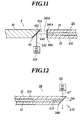
- Fig. 12 is a cross sectional view showing the configuration of an optical waveguide cable 2B of a conventional optical cable.
- the optical waveguide cable 2B serving as a transmission path for light signals is composed of cladding layers 21, 22 and a core layer 231, and a mirror surface 24B oriented at an angle of 45 degrees relative to the optical path is provided at an end face thereof.
- the mirror surface 24B has a diced facet 241 formed by dicing the cladding layers 21, 22 and the core layer 231 using a blade having an angle of 45 degrees.
- Laser light emitted from a VCSEL (Vertical Cavity Surface Emitting LASER) 311 is reflected by the diced facet 241 and transmitted in the core layer 231.
- optical path conversion is achieved by reflection using a difference in the optical index between the air and the core layer 231 at the diced facet 241.
- laser light propagated in the core layer is reflected by a diced facet and made incident on a PD (Photo Diode) that is not shown in the drawing.
- PD Photo Diode
- the mirror surface be smoothed.
- One conceivable solution is, for example, to process the mirror surface using laser light.
- the method using laser light it has not been possible for the method using laser light to achieve high accuracy in the inclination angle of the mirror surface.
- Another conceivable solution is to polish the diced facet after it is formed.
- the method using polishing makes the process complex. For example, it is required to attach a waveguide once on a substrate in order to perform polishing. Such an increase in the complexity of the operation has caused an increase in the cost.
- Still another conceivable solution is to perform dicing using a finer dicing blade to decrease the surface unevenness.
- the material of the optical waveguide is a polymer
- a reduction in the scattering loss is also demanded not only in a mirror surface of an optical waveguide but also in a processed surface in a light transmissive surface (incident surface or exit surface) of an optical waveguide and an optical unit other than optical waveguides.
- An object of the present invention is to reduce the scattering loss at an end face of an optical unit for reflection or transmission and to form such an end face easily at a low cost.
- the optical unit includes a core serving as an optical waveguide and cladding with which the core is covered.
- the invention as recited in claim 3 is characterized in that in the optical device according to claim 2, the smoothing film has a refractive index equal to or nearly equal to the refractive index of the core.
- the invention as recited in claim 4 is characterized in that in the optical device according to claim 2 or 3, the core has a plurality of layers.
- the invention as recited in claim 5 is characterized in that in the optical waveguide device according to any one of claims 1 to 4, at least one of a light emitting unit for emitting light to the smoothing film, a light receiving unit for receiving light reflected by the smoothing film and a light transmitting unit for emitting light to or receiving light from the smoothing film.
- An optical device manufacturing method as recited in claim 6 is characterized by comprising:
- the optical unit forming step comprises a step of forming a core serving as an optical waveguide and cladding with which the core is covered as the optical unit.
- the invention as recited in claim 8 is characterized in that in the optical device manufacturing method according to claim 7, in the smoothing film forming step, the smoothing film is formed by a material having a refractive index equal to or nearly equal to the refractive index of the core.
- the invention as recited in claim 9 is characterized in that in the optical device manufacturing method according to claim 7 or 8, in the optical unit forming step, the core is formed as a plurality of layers.
- the invention as recited in claim 10 is characterized in that in the optical device manufacturing method according to any one of claims 6 to 9, in the smoothing film forming process, the smoothing surface is formed by any one of dropping a liquid material of the smoothing film onto the processed surface, coating and spray.
- the core since the core includes a plurality of layers, light transmission in a plurality of optical waveguide can be achieved.
- the smoothing film can be formed easily with high precision by any one of the following:
- FIG. 1 shows the configuration of optical cable 1 according to the embodiment.
- the optical cable 1 connects two printed wiring boards 5 and is composed of an optical waveguide cable 2 serving as an optical waveguide device and connectors 3 provided at both ends thereof.
- the connector 3 is fitted in a socket 6 mounted on the printed wiring board 5.
- an IC Integrated Circuit
- the optical waveguide cable 2 is formed in a film like shape, and the optical waveguide provided in it functions as a transmission path of light that is transmitted and received between the connectors 3 provided at its both ends.
- the connector 3 is equipped with transmission/reception subassembly 3a that performs photoelectric conversion.
- the transmission/reception subassembly 3 converts an electrical signal input from the printed wiring board 5 into light and transmits light to the connector 3 that is located at the other end through the optical waveguide cable 2.
- the transmission/reception subassembly 3 also receives light transmitted through the optical waveguide cable from the connector 3 that is located at the other end, converts it into an electrical signal and output it to the printed wiring board 5.
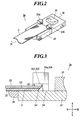
- Fig. 2 is a perspective view showing the configuration of the connection portion of the optical waveguide cable 2 and the transmission/reception subassembly 3a in the connector 3.
- Fig. 3 is a cross sectional view taken along line III-III, showing the configuration of the transmission/reception subassembly 3a shown in Fig. 2 .
- the end portion of the optical waveguide cable 2 is disposed between the mounting surface of a sub board 32 and a light emitting element 31a serving as a light emitting unit or a light receiving element 31b serving as a light receiving unit.
- the optical waveguide cable 2 is attached on and along the mounting surface in such a way that its film surface on the cladding layer 21 side is in contact with the sub board 32.
- the optical waveguide cable 2 is composed of cladding layers (or cladding) 21, 22 and a core layer (or core) 23 and has a mirror surface portion 24 at its end.
- the outer circumference of the optical waveguide cable 2 is covered with a resin film that is not shown in the drawings.
- the resin film which serves as a device cover, is made of a flexible material such as a polyimide or PET (poly Ethylene Terephthalate).
- the cladding layers 21, 22 and the core layer 23 are made of a resin or the like such as a polyimide resin, polysilane resin, epoxy resin or acrylate resin.
- the core layer 23 is formed straightly between the cladding layers 21, 22 and constitutes an optical waveguide.
- the material of the core layer 23 is arranged in such a way that it has a refractive index different from that of the cladding layers 21, 22. In this way, the core layer 23 is circumferentially surrounded by the cladding layers 21, 22 that have a different refractive index, so that light emitted into the core layer 23 can be propagated in one direction without loss.
- the core layer functioning as a transmission path for light emitted from the light emitting element 31a will be denoted as core layer 231 and the core layer functioning as a transmission path for light to be received by the light receiving element 31b will be denoted as core layer 232.
- the mirror surface portion 24 constitutes an optical path converting unit that reflects the light transmitted through the core layer 23 to introduce it to the light receiving element 31b located above the optical waveguide cable 2 or reflects the light emitted from the light emitting element 31a to introduce it into the core layer 23.
- the optical waveguide of the optical waveguide cable 2 refers to the light transmission path including the core layer 23 and the path of light in the cladding layer 22 introduced by the mirror surface portion 24.
- the mirror surface portion 24 is formed by cutting the end face of the optical waveguide cable 2 at an inclination angle of, for example, 45 degrees using a blade and forming a smoothing film 242.
- the transmission/reception subassembly 3a is an assembly in which the light emitting element 31a, the light receiving element 31b and an IC 33 are mounted on the sub board 32 as shown in Fig. 2 .
- the transmission/reception subassembly 3a performs mutual conversion between an electrical signal input/output to/from the printed wiring board 5 and light input/output through the optical waveguide cable 2.
- the light emitting element 31a is provided with a VCSEL 311 serving as a photoelectric conversion element that converts an electrical signal into a light signal.
- the light emitting element 31a emits light corresponding to an electrical signal input from the printed wiring board 5 in the Z-to-Y direction as shown in Fig. 3 .
- the optical path of the light emitted from the light emitting element 31a is converted by the mirror surface portion 24 and transmitted in the W-to-X direction.
- the photoelectric conversion element provided in the light emitting element 31a is not limited to the VCSEL, but it may be another type of photoelectric conversion element that converts an electrical signal into a light signal.
- the light receiving element 31b is provided with a PD 312 serving as a photoelectric conversion element that converts a light signal into an electrical signal.
- the light receiving element 31b receives the light that has been transmitted through the core layer 23 of the optical waveguide cable 2 in the X-to-W direction and undergone optical path conversion into the Y-to-Z direction, and generates an electrical signal corresponding to the received light quantity.
- the photoelectric conversion element provided in the light receiving element 31b is not limited to the PD, but it may be another type of photoelectric conversion element that converts an electrical signal into a light signal.
- a configuration in which a plurality of light emitting elements 31a and a plurality of light receiving elements 31b may be provided to perform two-way light transmission in a plurality of channels may be adopted, or alternatively a configuration in which a transmission/reception subassembly 3a at one end of the optical cable 1 is provided with only a light emitting element 31a and a transmission/reception subassembly 3a at the other end is provided with only a light receiving element 31b to perform one-way light transmission may be adopted.
- the height position of the photoelectric conversion element 31 is determined in accordance with the height of the optical waveguide cable 2 from the mounting surface. Specifically, the photoelectric conversion element 31 is disposed in such a way as to be spaced from the mounting surface of the sub board 32 with a bump 34 between, and the height of the photoelectric conversion element 31 has been adjusted in such a way as to be higher than the height corresponding to the thickness of the optical waveguide cable 2.
- the positions of the light emitting element 31a and the light receiving element 31b on the mounting surface of the board is determined in such a way that the optical axis of the light transmitted between the optical waveguide of the optical waveguide cable 2 and the VCSEL 311 of the light emitting element 31a and the optical axis of the light transmitted between the optical waveguide of the optical waveguide cable 2 and the PD 312 of the light receiving element 31b coincide with each other with reference to the mount position of the optical waveguide cable 2 on the mounting surface of the sub board 32.
- the height position of the photoelectric conversion element 31 can be adjusted by changing the size of the bump 34. This means that it is possible to control the optical path distance between the optical waveguide cable 2 and the light emitting element 31a/light receiving element 31b by adjusting the bump 34. Thus, the distance can be determined in such a way that the optical coupling efficiency between the optical waveguide cable 2 and the light emitting element 31a/light receiving element 31b is maximized.
- the bump 34 is made of an electrically conductive material and provides electrical connection between an electrode of the photoelectric conversion element 31 and an electrode provided on the sub board 32 (these electrodes being not shown in the drawings).
- the bump 34 may be made of a metal such as Au, for example.
- the gap between the optical waveguide cable 2 and the light emitting element 31a/light receiving element 31b is filled with an optical path forming material 35.
- the optical path forming material 35 is a light refractive medium such as, for example, a light curing resin.
- the material for the optical path forming material 35 is selected to have a relatively large refractive index as compared to the air, namely it has a refractive index, for example, nearly equal to the cladding layer 22 of the optical waveguide cable 2.
- Providing the optical path forming material 35 enables control for suppressing an increase in the exit diameter of the light traveling along the optical path between the optical waveguide cable and the light emitting element 31a/light receiving element 31b.
- a reinforcing material 36 that supports the optical waveguide cable is provided at the disjunction portion between the sub board 32 and the optical waveguide cable 2.
- Fig. 4A is a cross sectional view showing the configuration of the light transmitting section of the optical waveguide cable 2.
- Fig. 4B is a cross sectional view showing the configuration of the light receiving section of the optical waveguide cable 2.
- a mirror surface portion 24 is formed on the end face of the cladding layers 21, 22 and the core layer 231 serving as an optical unit.
- the mirror surface portion 24 is oriented at an angle of 45 degrees relative to the optical path.
- the mirror surface portion 24 includes a diced facet 241 and a smoothing film 242 formed on the diced facet 241.
- the diced facet 241 in the form of a processed surface is a facet that has been formed by dicing, and its surface is a rough surface with unevenness.
- the smoothing film 242 is a film to smooth the rough surface of the diced facet 241.
- the material of the smoothing film 242 is, for example, a refractive index adjusting material, a polyimide resin (e.g. polyimide fluoride), a polysilane resin or an epoxy resin (e.g. ultraviolet curing resin).
- the material of the smoothing film 242 is a viscous liquid material, as will be described later.
- the smoothing film 242 have a refractive index nearly equal to that of the core layer 23 (231, 232). This is desirable in order to make the difference in the refractive index between the diced facet 241 and the smoothing film little to thereby reduce scattering on the diced facet 241.
- the refractive index of the smoothing film 242 is designed to be equal to the refractive index of the core layer or approximately 1.51.
- laser light L11 emitted from the VCSEL 311 is reflected by the smoothing film 242 of the mirror surface portion at a right angle, and thereafter introduced as reflected light L12 into the core layer 231 and transmitted therein.
- a mirror surface portion 24 is formed on the end face of the cladding layers 21, 22 and the core layer 232 in the same manner as in the light transmitting section of the optical waveguide cable 2.
- the laser light L21 having been propagated in the core layer 232 is reflected by the smoothing film 242 of the mirror surface, and thereafter introduced as reflected light L22 to the PD 312 and received by it.
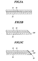
- Fig. 5A shows an optical waveguide cable in which a mirror surface portion 24 has not been formed yet.
- Fig. 5B shows the optical waveguide cable in which a diced facet 241 has been formed.
- Fig. 5C shows the optical waveguide cable on which the mirror surface portion 24 has been formed.
- an optical waveguide cable having cladding layers 21, 22 and a core layer 23 (231, 232) is manufactured.
- the cladding layer 22 is formed on a substrate such as a silicon substrate by spin coating and heat treatment etc.
- a core film is formed on the whole area of the cladding layer 22 by spin coating and baking etc, and the core layer 23 is formed in a waveguide pattern by photolithography.
- the cladding layer 21 is formed on the cladding layer 22 and the core layer 23 by spin coating and baking etc.
- the cladding layers 21, 22 and the core layer 23 are separated as the optical waveguide cable from the substrate.
- the optical waveguide cable is manufactured in the form of a flexible film.
- the optical waveguide cable thus formed is cut by dicing using a blade arranged at an angle of 45 degrees, so that a diced facet 241 is formed as the end face thereof.
- the diced facet 241 has a rough surface inclined at an angle of 45 degrees relative to the optical path (or the core layer 23).
- a liquid material for forming the smoothing film 242 is dropped on the diced facet 241.
- the position of the diced facet 241 is adjusted in such a way that it is oriented to be perpendicular or oblique with respect to the direction of dropping of the material for forming the smoothing film 242, and then the material for forming the smoothing film 242 is dropped.
- the diced facet 241 is covered with the liquid material.
- the liquid material for forming the smoothing film 242 is an ultraviolet curing resin
- the liquid material with which the diced facet 241 is covered is irradiated with ultraviolet light so as to be cured, and additionally heat-treated so as to be stabilized.
- the smoothing film 242 is formed, and the optical waveguide cable 2 is produced.
- optical waveguide cable 2 thus manufactured is attached to the transmission/reception subassembly 3a of the connector 3, whereby the optical cable 1 is produced.
- the material for forming the smoothing film 242 is a liquid material having viscosity and adhesiveness, preferably a material having a low viscosity. If a material having a viscosity as high as, for example, 770 cP is used, the material (and the smoothing film 242) will become convex on the diced facet 241, which deteriorates the function of the mirror surface.
- the process of forming the smoothing film 242 may be performed before or after the optical waveguide cable is mounted on the optical cable 1, but it is desirable that this process be performed during the mounting in order to mount the optical waveguide cable at the optimum position.
- the process of forming the smoothing film 242 is not limited to that performed by dropping the material, but it may be formed in other ways, such as coating (e.g. spin coating) spray etc.
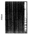
- Fig. 6A shows an SEM image of the mirror surface portion provided with only the diced facet.
- Fig. 6B shows an SEM image of the mirror surface portion 24 provided with the smoothing film 242.
- the SEM image of the surface shows streak-like unevenness caused by dicing.
- the surface is smoothed and the SEM image of the surface does not show streak-like unevenness.
- a dust portion formed on the smoothing film 242 is intentionally shown in the bottom portion of the SEM image to demonstrate that the image is in focus. In the dust portion of the smoothing film 242, streak-like unevenness can be seen. It will be appreciated from this that the central and upper portion of the SEM image is in focus.
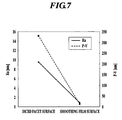
- Fig. 7 shows the roughness of the mirror surface portion 24 provided with only the diced facet and the mirror surface portion 24 provided with the smoothing film 242.
- values of Ra that is, roughness, or average surface roughness
- P-V values the maximum height difference
- Fig. 8 shows the quantity of light incident on the PD 312 for the optical waveguide cable having the mirror surface portion provided with only the diced facet and the optical waveguide cable 2 having the mirror surface portion 24 provided with the smoothing film 24.
- the quantity of light incident on the PD in the optical waveguide cable 2 having the mirror surface portion 24 provided with the smoothing film 242 was larger than that in the optical waveguide cable having the mirror surface portion provided with only the diced facet, and the loss of light quantity through reflection in the mirror surface portion was reduced by 5.3 dB.
- the optical waveguide cable 2 has the smoothing film 242 on the diced facet 241 of the core layer 23 and the cladding layers 21, 22, scattering loss in the mirror surface portion 24 can be reduced, and the mirror surface portion 24 can be produced easily at a low cost.
- the smoothing film 242 has a refractive index nearly equal to that of the core layer 23, scattering loss in the mirror surface portion 24 can further be reduced.
- optical cable 1 is equipped with the VCSEL 311 and the PD 312, light transmission with a reduced scattering loss in the mirror surface portion 24 can be easily realized.
- the smoothing film 242 can be produced easily with high precision by any one of the following methods: dropping a material for forming the smoothing film 242 on the diced facet, coating and spray.
- Fig. 9 is a cross sectional view showing the configuration of an optical waveguide cable 2 using an optical fiber 7.
- the optical fiber 7 has a core 71 in the form of a center core, a cladding 72 formed in an annular shape to cover the core 71 at the center and a not-shown jacket layer with which the cladding 72 is covered. In an end portion thereof, the jacket layer is removed when to be used.
- Laser light L3 emitted from a not-shown light source provided upstream of the optical fiber 7 is made incident on the optical waveguide cable 2 through the core 71 of the optical fiber 7, reflected by a smoothing film 242 in the mirror surface portion 24 and transmitted in the core layer 23.
- laser light emitted from the not-shown light source upstream of the optical waveguide cable 2 is transmitted through the core layer 23, reflected by the smoothing film 242 in the mirror surface portion 24 and made incident on the core 71 of the optical fiber 7 so as to be transmitted.
- Fig. 10 is a cross sectional view showing the configuration of an optical waveguide cable 8.
- the optical waveguide cable 8 has cladding layers 81, 82, 83, a core layer 84 provided between the cladding layers 81 and 82 and a core layer 85 provided between the cladding layers 82 and 83, and a mirror surface portion 86 oriented at an angle of 45 degrees relative to the optical path is provided.
- the mirror surface portion 86 includes a diced facet 861 and a smoothing film 862 formed on the diced facet 861.
- laser light L4 emitted from a VCSEL 311 is reflected by the smoothing film 862 in the mirror surface portion 86, and the reflected light is transmitted in the core layer 84.
- Laser light L5 emitted from a VCSEL 313 is reflected by the smoothing film 862 in the reflection surface portion 86, and the reflected light is introduced into and transmitted in the core layer 85.
- light signals having been separately transmitted through two core layers 84, 85 of the optical waveguide cable 8 are reflected by the smoothing film 862 in the mirror surface portion 86, introduced to two not-shown PDs and received by them separately.
- the two core layers are provided as above, light transmission can be performed in two optical waveguides. Furthermore, three or more core layers may be provided in an optical waveguide cable.
- the mirror surface portion 24 having a diced facet 241 and the smoothing film 242 is provided in the optical waveguide cable 2, the present invention is not limited to this.
- a mirror surface portion having a diced facet and a smoothing film may be applied to an optical fiber or an optical waveguide device such as an optical waveguide circuit provided on a substrate.
- the optical waveguide cable 2 provided with the mirror surface portion 24 having the diced facet 241 and the smoothing film 242 is used in the optical cable 1 serving as an optical transceiver
- the present invention is not limited to this.
- the present invention can be applied to all the optical devices that utilize reflection by a core layer and the air.
- the mirror surface portion 24 is oriented at an angle of 45 degrees relative to the optical path, the present invention is not limited to this.
- the mirror surface may be oriented at an angle other than 45 degrees (e.g. 0, 10, 30 or 90 degrees).
- Fig. 11 is a cross sectional view showing the configuration of a reflector 9 and an optical waveguide cable 2A.
- a structure provided with a reflector 9 and an optical waveguide cable 2A may be adopted.
- the reflector 9 includes a reflector body 91 and a mirror surface portion 92.
- the reflector body 91 is made of a material such as quartz or a polymer.
- As the material of the reflector body 91 a material having an appropriate refractive index that reflects light that is incident on it from the air is selected.
- the mirror surface portion 92 includes a diced facet 921 oriented at an angle of 45 degrees relative to the optical path and a smoothing surface 922 formed on the diced facet 921.
- the optical waveguide cable 2B has cladding layers 21, 22 and a core layer 23, and an end surface portion 24A is provided at the end face of the cladding layers 21, 22 and the core layer 231.
- the end surface portion 24A includes a diced facet 241A oriented at an angle of 90 degrees relative to the optical path and a smoothing film 242A formed on the diced facet 241.
- laser light L61 emitted from a VCSEL 314 is reflected by the surface of the smoothing film 922 in the reflector 9 to generate reflected light L62.
- the reflected light L62 is made incident on the core layer 23 through the end surface portion 24A of the optical waveguide cable 2A and transmitted in the core layer 23.
- a reduction in scattering loss at the diced facets 921, 241A is achieved.
- the optical waveguide cable 2 may be provided with a mirror surface portion further including a metal film (e.g. gold, silver or aluminum) formed by vapor deposition on the smoothing film 242 formed on the diced facet 241.
- a metal film e.g. gold, silver or aluminum
- scattering loss can further be reduced as compared to the configuration in which the mirror surface portion 24 includes the diced facet 241 and the smoothing film 242.
- an optical fiber or a planar lightwave circuit may be used as the optical unit provided with a diced facet and a smoothing film therefor.
- the optical waveguide cable 2 having a processed surface in the form of a diced facet 241 has been described, the present invention is not limited to this.
- the processed surface may be a surface formed by cutting using a laser or a microtome.
- the optical device and the optical device manufacturing method according to the present invention are suitable for devices used in optical communication and the method for manufacturing such devices.
Landscapes
- Physics & Mathematics (AREA)
- General Physics & Mathematics (AREA)
- Optics & Photonics (AREA)
- Condensed Matter Physics & Semiconductors (AREA)
- Electromagnetism (AREA)
- Optical Integrated Circuits (AREA)
- Optical Couplings Of Light Guides (AREA)
- Semiconductor Lasers (AREA)
Applications Claiming Priority (2)
| Application Number | Priority Date | Filing Date | Title |
|---|---|---|---|
| JP2006122102A JP2007293108A (ja) | 2006-04-26 | 2006-04-26 | 光学装置及び光学装置の製造方法 |
| PCT/JP2007/056779 WO2007125716A1 (fr) | 2006-04-26 | 2007-03-29 | Dispositif optique et procede de fabrication dudit dispositif optique |
Publications (1)
| Publication Number | Publication Date |
|---|---|
| EP2012154A1 true EP2012154A1 (fr) | 2009-01-07 |
Family
ID=38655251
Family Applications (1)
| Application Number | Title | Priority Date | Filing Date |
|---|---|---|---|
| EP07740217A Withdrawn EP2012154A1 (fr) | 2006-04-26 | 2007-03-29 | Dispositif optique et procede de fabrication dudit dispositif optique |
Country Status (6)
| Country | Link |
|---|---|
| US (1) | US20090067799A1 (fr) |
| EP (1) | EP2012154A1 (fr) |
| JP (1) | JP2007293108A (fr) |
| KR (1) | KR100973050B1 (fr) |
| CN (1) | CN101410741A (fr) |
| WO (1) | WO2007125716A1 (fr) |
Families Citing this family (13)
| Publication number | Priority date | Publication date | Assignee | Title |
|---|---|---|---|---|
| KR100973631B1 (ko) * | 2005-07-27 | 2010-08-02 | 미쓰미덴기가부시기가이샤 | 도파로 필름 케이블 |
| US8090266B2 (en) * | 2007-11-26 | 2012-01-03 | Fujitsu Limited | Optically coupling components of a transceiver |
| JP5136260B2 (ja) * | 2008-07-24 | 2013-02-06 | 富士ゼロックス株式会社 | 光導波路フィルム、及び光送受信モジュール |
| JP5109982B2 (ja) * | 2008-10-09 | 2012-12-26 | 日立電線株式会社 | ミラー付き光伝送体の製造方法 |
| KR20120123125A (ko) | 2010-02-23 | 2012-11-07 | 파나소닉 주식회사 | 광 모듈 |
| US9247638B2 (en) * | 2010-11-10 | 2016-01-26 | Xyratex Technology Limited | Optical printed circuit board and a method of manufacturing an optical printed circuit board |
| US9046668B2 (en) * | 2011-06-22 | 2015-06-02 | Panasonic Intellectual Property Management Co., Ltd. | Optical module |
| WO2013042364A1 (fr) * | 2011-09-20 | 2013-03-28 | 日本電気株式会社 | Module de transmission optique |
| US10222294B2 (en) * | 2015-03-31 | 2019-03-05 | Mellanox Technologies Silicon Photonics Inc. | Wafer level testing of optical devices |
| IT201700105367A1 (it) * | 2017-09-20 | 2019-03-20 | St Microelectronics Srl | Procedimento per produrre guide d'onda ottiche, sistema e dispositivo corrispondenti |
| US10877218B2 (en) | 2019-03-26 | 2020-12-29 | Stmicroelectronics S.R.L. | Photonic devices and methods for formation thereof |
| CN114205990B (zh) * | 2020-09-17 | 2024-03-22 | 深南电路股份有限公司 | 线路板及其制备方法 |
| US11957804B2 (en) * | 2020-09-28 | 2024-04-16 | The Boeing Company | Optical disinfection systems having side-emitting optical fiber coupled to high-energy UV-C laser diode |
Family Cites Families (18)
| Publication number | Priority date | Publication date | Assignee | Title |
|---|---|---|---|---|
| JPS6012513A (ja) * | 1983-07-04 | 1985-01-22 | Omron Tateisi Electronics Co | 光導波路の端面研磨装置 |
| JPS63191111A (ja) | 1987-02-04 | 1988-08-08 | Nippon Telegr & Teleph Corp <Ntt> | 光結合器 |
| JP2699405B2 (ja) * | 1988-05-12 | 1998-01-19 | ソニー株式会社 | 陰極線管 |
| JPH01312514A (ja) | 1988-06-10 | 1989-12-18 | Sumitomo Electric Ind Ltd | 光ファイバ集積装置 |
| KR100236432B1 (ko) * | 1996-07-31 | 1999-12-15 | 미야즈 쥰이치로 | 광학 편광기, 이의 제조 방법 및 광학 편광기 제조용 블레이드 |
| JP3753508B2 (ja) * | 1996-07-31 | 2006-03-08 | 日本電信電話株式会社 | 光路変換素子の作製方法、および光路変換素子作製用のブレード |
| JP4752092B2 (ja) * | 2000-07-31 | 2011-08-17 | 株式会社トッパンNecサーキットソリューションズ | 光導波路接続構造及び光素子実装構造 |
| JP3748528B2 (ja) * | 2001-10-03 | 2006-02-22 | 三菱電機株式会社 | 光路変換デバイスおよびその製造方法 |
| JP2004133103A (ja) * | 2002-10-09 | 2004-04-30 | Sony Corp | 高分子光導波路及びその作製方法 |
| JP2004145548A (ja) * | 2002-10-23 | 2004-05-20 | Mitsubishi Chemicals Corp | 情報記録媒体及びその製造方法 |
| JP2005321560A (ja) * | 2004-05-07 | 2005-11-17 | Fuji Xerox Co Ltd | 受発光素子付き高分子光導波路モジュール |
| JP2006011210A (ja) * | 2004-06-29 | 2006-01-12 | Fuji Xerox Co Ltd | 発光素子及びモニター用受光素子付き高分子光導波路モジュール |
| JP2006017885A (ja) * | 2004-06-30 | 2006-01-19 | Fuji Xerox Co Ltd | 導波路フィルム型光モジュール、光導波路フィルム及びその製造方法 |
| JP2006184773A (ja) * | 2004-12-28 | 2006-07-13 | Mitsui Chemicals Inc | 光導波路およびこれを備えた光電気混載基板 |
| US7343060B2 (en) * | 2005-03-04 | 2008-03-11 | Fuji Xerox Co., Ltd. | Light transmission and reception module, sub-mount, and method of manufacturing the sub-mount |
| JP2007027398A (ja) * | 2005-07-15 | 2007-02-01 | Fuji Xerox Co Ltd | 光学部品実装用サブマウント、及び光送受信モジュール |
| JP2007033688A (ja) * | 2005-07-25 | 2007-02-08 | Fuji Xerox Co Ltd | 光導波路フィルム、及び光送受信モジュール |
| JP2007033698A (ja) * | 2005-07-25 | 2007-02-08 | Fuji Xerox Co Ltd | 光学部品実装用サブマウント、及び光送受信モジュール |
-
2006
- 2006-04-26 US US12/225,629 patent/US20090067799A1/en not_active Abandoned
- 2006-04-26 JP JP2006122102A patent/JP2007293108A/ja active Pending
-
2007
- 2007-03-29 CN CNA2007800107435A patent/CN101410741A/zh active Pending
- 2007-03-29 KR KR1020087021655A patent/KR100973050B1/ko not_active Expired - Fee Related
- 2007-03-29 WO PCT/JP2007/056779 patent/WO2007125716A1/fr not_active Ceased
- 2007-03-29 EP EP07740217A patent/EP2012154A1/fr not_active Withdrawn
Non-Patent Citations (1)
| Title |
|---|
| See references of WO2007125716A1 * |
Also Published As
| Publication number | Publication date |
|---|---|
| KR20080094939A (ko) | 2008-10-27 |
| CN101410741A (zh) | 2009-04-15 |
| JP2007293108A (ja) | 2007-11-08 |
| WO2007125716A1 (fr) | 2007-11-08 |
| US20090067799A1 (en) | 2009-03-12 |
| KR100973050B1 (ko) | 2010-07-29 |
Similar Documents
| Publication | Publication Date | Title |
|---|---|---|
| EP2012154A1 (fr) | Dispositif optique et procede de fabrication dudit dispositif optique | |
| US8827572B2 (en) | Side coupling optical fiber assembly and fabrication method thereof | |
| US8755644B2 (en) | Silicon based optical vias | |
| KR101588348B1 (ko) | 광자 유도 장치 | |
| EP2426537B1 (fr) | Module de coupleur optique doté d'une structure de guide d'ondes optique | |
| KR100802199B1 (ko) | 광모듈 및 그 제조방법 | |
| US20070085215A1 (en) | Silicon based optical vias | |
| JP5946611B2 (ja) | 光レセプタクルおよびこれを備えた光モジュール | |
| KR100818622B1 (ko) | 광 인쇄회로기판 및 그 제작방법 | |
| JP2006506657A (ja) | 光ファイバーとの半導体装置の能動的光学整合のための一体化プラットホーム | |
| CA2651023A1 (fr) | Element de carte de circuits imprimes comprenant un composant optoelectronique et un guide d'ondes optique | |
| US20180372966A1 (en) | Optical device, optical processing device, and method of producing the optical device | |
| CN100476473C (zh) | 光波导、光缆模块及光波导的制造方法 | |
| WO2013140922A1 (fr) | Réceptacle optique et module optique équipé de ce dernier | |
| US7856164B2 (en) | Waveguide device | |
| JP5395042B2 (ja) | 光路変換デバイスの製造方法 | |
| WO2005036212A2 (fr) | Appareil a fibre optique/photodetecteur a efficacite de couplage optique ameliore et procede de fabrication correspondant | |
| US20090304323A1 (en) | Optical coupling structure and substrate with built-in optical transmission function, and method of manufacturing the same | |
| US20050281513A1 (en) | Module for transmitting and receiving optical signal based on optical fiber having slanted surface and method of manufacturing the same | |
| US11953737B2 (en) | Systems and methods for coupling light | |
| US20090116787A1 (en) | Optical Waveguide Device and Method for Fabricating Optical Waveguide Device | |
| WO2017122809A1 (fr) | Module de conversion photoélectrique et câble optique actif | |
| JP2007178950A (ja) | 光配線基板および光配線モジュール | |
| JP2005078022A (ja) | 光導波モジュールおよびその製造方法 | |
| KR100970395B1 (ko) | 광도파로 디바이스 및 광도파로 디바이스 제조 방법 |
Legal Events
| Date | Code | Title | Description |
|---|---|---|---|
| PUAI | Public reference made under article 153(3) epc to a published international application that has entered the european phase |
Free format text: ORIGINAL CODE: 0009012 |
|
| 17P | Request for examination filed |
Effective date: 20080929 |
|
| AK | Designated contracting states |
Kind code of ref document: A1 Designated state(s): AT BE BG CH CY CZ DE DK EE ES FI FR GB GR HU IE IS IT LI LT LU LV MC MT NL PL PT RO SE SI SK TR |
|
| AX | Request for extension of the european patent |
Extension state: AL BA HR MK RS |
|
| DAX | Request for extension of the european patent (deleted) | ||
| RBV | Designated contracting states (corrected) |
Designated state(s): DE FR GB |
|
| STAA | Information on the status of an ep patent application or granted ep patent |
Free format text: STATUS: THE APPLICATION IS DEEMED TO BE WITHDRAWN |
|
| 18D | Application deemed to be withdrawn |
Effective date: 20111001 |