EP2006710A2 - Radiation image conversion panel, scintillator panel, and radiation image sensor - Google Patents
Radiation image conversion panel, scintillator panel, and radiation image sensor Download PDFInfo
- Publication number
- EP2006710A2 EP2006710A2 EP08010625A EP08010625A EP2006710A2 EP 2006710 A2 EP2006710 A2 EP 2006710A2 EP 08010625 A EP08010625 A EP 08010625A EP 08010625 A EP08010625 A EP 08010625A EP 2006710 A2 EP2006710 A2 EP 2006710A2
- Authority
- EP
- European Patent Office
- Prior art keywords
- scintillator
- aluminum substrate
- radiation image
- radiation
- panel
- Prior art date
- Legal status (The legal status is an assumption and is not a legal conclusion. Google has not performed a legal analysis and makes no representation as to the accuracy of the status listed.)
- Withdrawn
Links
- 230000005855 radiation Effects 0.000 title claims abstract description 72
- 238000006243 chemical reaction Methods 0.000 title claims abstract description 18
- 239000000758 substrate Substances 0.000 claims abstract description 88
- 229910052782 aluminium Inorganic materials 0.000 claims abstract description 80
- XAGFODPZIPBFFR-UHFFFAOYSA-N aluminium Chemical compound [Al] XAGFODPZIPBFFR-UHFFFAOYSA-N 0.000 claims abstract description 80
- 230000002787 reinforcement Effects 0.000 claims description 13
- TWNQGVIAIRXVLR-UHFFFAOYSA-N oxo(oxoalumanyloxy)alumane Chemical compound O=[Al]O[Al]=O TWNQGVIAIRXVLR-UHFFFAOYSA-N 0.000 claims description 7
- 230000001681 protective effect Effects 0.000 description 13
- OAICVXFJPJFONN-UHFFFAOYSA-N Phosphorus Chemical compound [P] OAICVXFJPJFONN-UHFFFAOYSA-N 0.000 description 8
- 238000003384 imaging method Methods 0.000 description 8
- -1 polyparaxylylene Polymers 0.000 description 7
- 239000000463 material Substances 0.000 description 5
- 238000000034 method Methods 0.000 description 5
- 230000000694 effects Effects 0.000 description 4
- 238000004519 manufacturing process Methods 0.000 description 4
- OKTJSMMVPCPJKN-UHFFFAOYSA-N Carbon Chemical compound [C] OKTJSMMVPCPJKN-UHFFFAOYSA-N 0.000 description 3
- VYPSYNLAJGMNEJ-UHFFFAOYSA-N Silicium dioxide Chemical compound O=[Si]=O VYPSYNLAJGMNEJ-UHFFFAOYSA-N 0.000 description 3
- 239000013078 crystal Substances 0.000 description 3
- 230000007423 decrease Effects 0.000 description 3
- QAOWNCQODCNURD-UHFFFAOYSA-N Sulfuric acid Chemical compound OS(O)(=O)=O QAOWNCQODCNURD-UHFFFAOYSA-N 0.000 description 2
- GWEVSGVZZGPLCZ-UHFFFAOYSA-N Titan oxide Chemical compound O=[Ti]=O GWEVSGVZZGPLCZ-UHFFFAOYSA-N 0.000 description 2
- 239000000853 adhesive Substances 0.000 description 2
- 230000001070 adhesive effect Effects 0.000 description 2
- LYQFWZFBNBDLEO-UHFFFAOYSA-M caesium bromide Chemical compound [Br-].[Cs+] LYQFWZFBNBDLEO-UHFFFAOYSA-M 0.000 description 2
- 229910052799 carbon Inorganic materials 0.000 description 2
- 239000004918 carbon fiber reinforced polymer Substances 0.000 description 2
- 230000007797 corrosion Effects 0.000 description 2
- 238000005260 corrosion Methods 0.000 description 2
- 238000010586 diagram Methods 0.000 description 2
- 230000003287 optical effect Effects 0.000 description 2
- 230000003647 oxidation Effects 0.000 description 2
- 238000007254 oxidation reaction Methods 0.000 description 2
- 238000007789 sealing Methods 0.000 description 2
- 239000004642 Polyimide Substances 0.000 description 1
- 229920002396 Polyurea Polymers 0.000 description 1
- 229910004541 SiN Inorganic materials 0.000 description 1
- 239000002390 adhesive tape Substances 0.000 description 1
- 239000003513 alkali Substances 0.000 description 1
- PNEYBMLMFCGWSK-UHFFFAOYSA-N aluminium oxide Inorganic materials [O-2].[O-2].[O-2].[Al+3].[Al+3] PNEYBMLMFCGWSK-UHFFFAOYSA-N 0.000 description 1
- 238000010000 carbonizing Methods 0.000 description 1
- 238000001444 catalytic combustion detection Methods 0.000 description 1
- 239000003610 charcoal Substances 0.000 description 1
- 229910052681 coesite Inorganic materials 0.000 description 1
- 238000004040 coloring Methods 0.000 description 1
- 210000002777 columnar cell Anatomy 0.000 description 1
- 239000000470 constituent Substances 0.000 description 1
- 229910052593 corundum Inorganic materials 0.000 description 1
- 230000008878 coupling Effects 0.000 description 1
- 238000010168 coupling process Methods 0.000 description 1
- 238000005859 coupling reaction Methods 0.000 description 1
- 229910052906 cristobalite Inorganic materials 0.000 description 1
- 238000000151 deposition Methods 0.000 description 1
- 230000002542 deteriorative effect Effects 0.000 description 1
- 239000003792 electrolyte Substances 0.000 description 1
- 230000001747 exhibiting effect Effects 0.000 description 1
- 239000006260 foam Substances 0.000 description 1
- 239000005350 fused silica glass Substances 0.000 description 1
- 239000011521 glass Substances 0.000 description 1
- 229910002804 graphite Inorganic materials 0.000 description 1
- 239000010439 graphite Substances 0.000 description 1
- 150000004820 halides Chemical class 0.000 description 1
- 238000010191 image analysis Methods 0.000 description 1
- 239000012535 impurity Substances 0.000 description 1
- 229910010272 inorganic material Inorganic materials 0.000 description 1
- 239000011147 inorganic material Substances 0.000 description 1
- 238000005304 joining Methods 0.000 description 1
- PQXKHYXIUOZZFA-UHFFFAOYSA-M lithium fluoride Inorganic materials [Li+].[F-] PQXKHYXIUOZZFA-UHFFFAOYSA-M 0.000 description 1
- 229910001635 magnesium fluoride Inorganic materials 0.000 description 1
- CPLXHLVBOLITMK-UHFFFAOYSA-N magnesium oxide Inorganic materials [Mg]=O CPLXHLVBOLITMK-UHFFFAOYSA-N 0.000 description 1
- 229910052751 metal Inorganic materials 0.000 description 1
- 239000002184 metal Substances 0.000 description 1
- 239000004033 plastic Substances 0.000 description 1
- 229920003023 plastic Polymers 0.000 description 1
- 229920000052 poly(p-xylylene) Polymers 0.000 description 1
- 229920001721 polyimide Polymers 0.000 description 1
- 230000002265 prevention Effects 0.000 description 1
- 229920005989 resin Polymers 0.000 description 1
- 239000011347 resin Substances 0.000 description 1
- 238000005096 rolling process Methods 0.000 description 1
- 239000000377 silicon dioxide Substances 0.000 description 1
- 229910052682 stishovite Inorganic materials 0.000 description 1
- 229910052716 thallium Inorganic materials 0.000 description 1
- 238000002834 transmittance Methods 0.000 description 1
- 229910052905 tridymite Inorganic materials 0.000 description 1
- 238000007740 vapor deposition Methods 0.000 description 1
- 125000006839 xylylene group Chemical group 0.000 description 1
- 229910001845 yogo sapphire Inorganic materials 0.000 description 1
Images


Classifications
-
- G—PHYSICS
- G01—MEASURING; TESTING
- G01T—MEASUREMENT OF NUCLEAR OR X-RADIATION
- G01T1/00—Measuring X-radiation, gamma radiation, corpuscular radiation, or cosmic radiation
- G01T1/16—Measuring radiation intensity
- G01T1/20—Measuring radiation intensity with scintillation detectors
- G01T1/202—Measuring radiation intensity with scintillation detectors the detector being a crystal
-
- H—ELECTRICITY
- H10—SEMICONDUCTOR DEVICES; ELECTRIC SOLID-STATE DEVICES NOT OTHERWISE PROVIDED FOR
- H10F—INORGANIC SEMICONDUCTOR DEVICES SENSITIVE TO INFRARED RADIATION, LIGHT, ELECTROMAGNETIC RADIATION OF SHORTER WAVELENGTH OR CORPUSCULAR RADIATION
- H10F30/00—Individual radiation-sensitive semiconductor devices in which radiation controls the flow of current through the devices, e.g. photodetectors
- H10F30/20—Individual radiation-sensitive semiconductor devices in which radiation controls the flow of current through the devices, e.g. photodetectors the devices having potential barriers, e.g. phototransistors
- H10F30/29—Individual radiation-sensitive semiconductor devices in which radiation controls the flow of current through the devices, e.g. photodetectors the devices having potential barriers, e.g. phototransistors the devices being sensitive to radiation having very short wavelengths, e.g. X-rays, gamma-rays or corpuscular radiation
-
- G—PHYSICS
- G01—MEASURING; TESTING
- G01T—MEASUREMENT OF NUCLEAR OR X-RADIATION
- G01T1/00—Measuring X-radiation, gamma radiation, corpuscular radiation, or cosmic radiation
- G01T1/16—Measuring radiation intensity
- G01T1/20—Measuring radiation intensity with scintillation detectors
Definitions
- the present invention relates to a radiation image conversion panel, a scintillator panel, and a radiation image sensor which are used in medical and industrial x-ray imaging and the like.
- x-ray sensitive films have conventionally been in use for medical and industrial x-ray imaging
- radiation imaging systems using radiation detectors have been coming into widespread use from the viewpoint of their convenience and storability of imaging results.
- pixel data formed by two-dimensional radiations are acquired by a radiation detector as an electric signal, which is then processed by a processor, so as to be displayed on a monitor.
- a typical radiation detector is one having a structure bonding a radiation image conversion panel (which will be referred to as "scintillator panel” in the following as the case may be), in which a scintillator for converting a radiation into visible light is formed on a substrate such as aluminum, glass, or fused silica, to an image pickup device.
- a radiation incident thereon from the substrate side is converted into light by the scintillator, and thus obtained light is detected by the image pickup device.
- a stimulable phosphor is formed on an aluminum substrate having a surface formed with an alumite layer.
- the radiation image conversion panel having a stimulable phosphor formed on a substrate will be referred to as "imaging plate" in the following as the case may be.
- the radiation image conversion panel in accordance with the present invention comprises an aluminum substrate, an alumite layer formed on a surface of the aluminum substrate, an intermediate film covering the alumite layer and having a radiation transparency and a light transparency, and a converting part provided on the intermediate film and adapted to convert a radiation image.
- the scintillator panel in accordance with the present invention comprises an aluminum substrate, an alumite layer formed on a surface of the aluminum substrate, an intermediate film covering the alumite layer and having a radiation transparency and a light transparency, and a scintillator provided on the intermediate film.
- the radiation image sensor in accordance with the present invention comprises a radiation image conversion panel including an aluminum substrate, an alumite layer formed on a surface of the aluminum substrate, an intermediate film covering the alumite layer and having a radiation transparency and a light transparency, and a converting part provided on the intermediate film and adapted to convert a radiation image; and an image pickup device for converting light emitted from the converting part of the radiation image conversion panel into an electric signal.
- Fig. 1 is a partly broken perspective view showing a scintillator panel (an example of radiation image conversion panel) in accordance with a first embodiment.
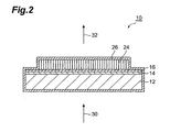
- Fig. 2 is a sectional view taken along the line II-II shown in Fig. 1 .
- the scintillator panel 10 comprises an aluminum substrate 12, an alumite layer 14 formed on a surface of the aluminum substrate 12, and an intermediate film 16 which is provided on the alumite layer 14 and has a radiation transparency.
- the alumite layer 14 and intermediate film 16 are in close contact with each other.
- the scintillator panel 10 also has a scintillator 24 (an example of a converting part adapted to convert a radiation image) provided on the intermediate film 16.
- the intermediate film 16 and scintillator 24 are in close contact with each other.
- the aluminum substrate 12, alumite layer 14, intermediate film 16, and scintillator 24 are totally sealed with a protective film 26.
- the scintillator 24 converts the radiation image into a light image.
- the radiation 30 successively passes through the protective film 26, aluminum substrate 12, alumite layer 14, and intermediate film 16, thereby reaching the scintillator 24.
- the light 32 emitted from the scintillator 24 is transmitted through the protective film 26 to the outside, while passing through the intermediate film 16, so as to be reflected by the alumite layer 14 and aluminum substrate 12 to the outside.
- the scintillator panel 10 is used for medical and industrial x-ray imaging and the like.
- the aluminum substrate 12 is a substrate mainly made of aluminum, but may contain impurities and the like.
- the thickness of the aluminum substrate 12 is 0.3 to 1.0 mm.
- the scintillator 24 tends to be easy to peel off as the aluminum substrate 12 bends.
- the thickness of the aluminum substrate 12 exceeds 1.0 mm, the transmittance of the radiation 30 tends to decrease.
- Layer 14 is made of porous aluminum oxide formed by anodic oxidation of aluminum (i.e. alumite).
- the alumite layer 14 makes it harder to damage the aluminum substrate 12. If the aluminum substrate 12 is damaged, the reflectance of the aluminum substrate 12 will be less than a desirable value, whereby no uniform reflectance will be obtained within the surface of the aluminum substrate 12. Whether the aluminum substrate 12 is damaged or not can be inspected visually, for example.
- the alumite layer 14 may be formed on the aluminum substrate 12 on only one side to be formed with the scintillator 24, on both sides of the aluminum substrate 12, or such as to cover the aluminum substrate 12 as a whole.
- Forming the alumite layer 14 on both sides of the aluminum substrate 12 can reduce the warpage and flexure of the aluminum substrate 12, and thus can prevent the scintillator 24 from being unevenly vapor-deposited. Forming the alumite layer 14 can also erase streaks occurring when forming the aluminum substrate 12 by rolling. Therefore, even when a reflecting film (a metal film and oxide layer) is formed on the aluminum substrate 12, a uniform reflectance can be obtained within the surface of the aluminum substrate 12 in the reflecting film.
- the thickness of the alumite layer 14 is 10 to 5000 nm. When the thickness of the alumite layer 14 is less than 10 nm, the damage prevention effect of the aluminum substrate 12 tends to decrease.
- the alumite layer 14 When the thickness of the alumite layer 14 exceeds 5000 nm, the alumite layer 14 tends to peel off in particular in corner parts of the aluminum substrate 12, thereby causing large cracks in the alumite layer 14 and deteriorating the moisture resistance of the alumite layer 14.
- the thickness of the alumite layer 14 is 1000 nm. The thickness of the alumite layer 14 is appropriately determined according to the size and thickness of the aluminum substrate 12.
- the alumite layer 14 may be colored with a dye or the like, for example.
- the alumite layer 14 is not colored, the light 32 is reflected by both of the surface of the alumite layer 14 and the surface of the aluminum substrate 12. Since the light 32 is reflected by the surface of the aluminum substrate 12, the luminance of the scintillator panel 10 improves in this case.
- the alumite layer 14 is colored black or the like, for example, on the other hand, the resolution can be enhanced, although the light 32 is absorbed so that the luminance of the scintillator panel 10 decreases.
- the alumite layer 14 may be provided with a desirable color so as to absorb a predetermined wavelength of light.
- the intermediate film 16 and protective film 26 are organic or inorganic films, which may be made of materials different from each other or the same material.
- the intermediate film 16 and protective film 26 are made of polyparaxylylene, for example, but may also be of xylylene-based materials such as polymonochloroparaxylylene, polydichloroparaxylylene, polytetrachloroparaxylylene, polyfluoroparaxylylene, polydimethylparaxylylene, and polydiethylparaxylylene.
- the intermediate film 16 and protective film 26 may be made of polyurea, polyimide, and the like, for example, or inorganic materials such as LiF, MgF 2 , SiO 2 , Al 2 O 3 , TiO 2 , MgO, and SiN.
- the intermediate film 16 and protective film 26 may also be formed by combining inorganic and organic films.
- the intermediate film 16 and protective film 26 have a thickness of 10 ⁇ m each.
- the intermediate film 16 reduces minute irregularities of the alumite layer 14, thereby advantageously acting for forming the scintillator 24 having a uniform thickness on the alumite layer 14.
- the scintillator 24 is smaller than the aluminum substrate 12 when seen in the thickness direction of the aluminum substrate 12.
- the scintillator 24 is constituted by a phosphor which converts the radiation into visible light and is made of a columnar crystal or the like of CsI doped with Tl, Na, or the like.
- the scintillator 24 has a structure provided with a forest of columnar crystals.
- the scintillator 24 may also be made of Tl-doped NaI, Tl-doped KI, or Eu-doped LiI.
- a stimulable phosphor such as Eu-doped CsBr may be used in place of the scintillator 24.
- the thickness of the scintillator 24 is preferably 100 to 1000 ⁇ m, more preferably 450 to 550 ⁇ m.
- the average column diameter of the columnar crystals constituting the scintillator 24 is 3 to 10 ⁇ m.
- the scintillator panel 10 comprises the aluminum substrate 12, the alumite layer 14 formed on the surface of the aluminum substrate 12, the intermediate film 16 covering the alumite layer 14 and having a radiation transparency and a light transparency, and the scintillator 24 provided on the intermediate film 16. Since the intermediate film 16 is provided between the alumite layer 14 and scintillator 24, the scintillator panel 10 can keep the alumite layer 14 and scintillator 24 from reacting with each other even if the alumite layer 14 is formed with cracks, pinholes, and the like. This can prevent the aluminum substrate 12 from corroding.
- Forming the alumite layer 14 can erase damages to the surface of the aluminum substrate 12, whereby uniform luminance and resolution characteristics can be obtained within the surface of the scintillator panel 10. Further, the intermediate film 16 can improve the flatness of the scintillator 24.
- the light 32 emitted from the scintillator 24 passes through the intermediate film 16, so as to be mainly reflected by the alumite layer 14 and aluminum substrate 12. Therefore, the wavelength and the like of the light 32 taken out from the scintillator panel 10 can be controlled by adjusting optical characteristics of the alumite layer 14. For example, the wavelength of the light 32 taken out from the scintillator panel 10 can be selected by coloring the alumite layer 14.
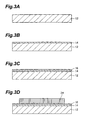
- Figs. 3A to 3D are process sectional views schematically showing an example of method of manufacturing the scintillator panel in accordance with the first embodiment. The method of manufacturing the scintillator panel 10 will now be explained with reference to Figs. 3A to 3D .
- the aluminum substrate 12 is prepared.
- the alumite layer 14 is formed by anodic oxidation on a surface of the aluminum substrate 12.
- the aluminum substrate 12 is electrolyzed by an anode in an electrolyte such as dilute sulfuric acid, so as to be oxidized.
- the alumite layer 14 may be dipped in a dye, so as to be colored. This can improve the resolution or enhance the luminance.
- the alumite layer 14 is subjected to a sealing process for filling the fine holes.
- the intermediate film 16 is formed on the alumite layer 14 by using CVD.
- the scintillator 24 is formed on the intermediate film 16 by using vapor deposition.
- the protective film 26 is formed by using CVD so as to seal the aluminum substrate 12, alumite layer 14, intermediate film 16, and scintillator 24 as a whole.
- the sealing with the protective film 26 can be realized by lifting the side of the aluminum substrate 12 opposite from the scintillator forming surface from a substrate holder at the time of CVD.
- An example of such method is one disclosed in U.S. Patent No. 6,777,690 . This method lifts the aluminum substrate 12 by using pins. In this case, no protective film is formed on minute contact surfaces between the aluminum substrate 12 and the pins.
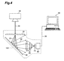
- Fig. 4 is a diagram showing an example of radiation image sensor including the scintillator panel in accordance with the first embodiment.
- the radiation image sensor 100 shown in Fig. 4 comprises the scintillator panel 10 and an image pickup device 70 which converts the light 32 emitted from the scintillator 24 of the scintillator panel 10 into an electric signal.
- the light 32 emitted from the scintillator 24 is reflected by a mirror 50, so as to be made incident on a lens 60.
- the light 32 is converged by the lens 60, so as to be made incident on the image pickup device 70.
- One or a plurality of lenses 60 may be provided.
- the radiation 30 emitted from a radiation source 40 such as x-ray source is transmitted through an object to be inspected which is not depicted.
- the transmitted radiation image is made incident on the scintillator 24 of the scintillator panel 10.
- the scintillator 24 emits a visible light image (the light 32 having a wavelength to which the image pickup device 70 is sensitive) corresponding to the radiation image.
- the light 32 emitted from the scintillator 24 is made incident on the image pickup device 70 by way of the mirror 50 and lens 60.
- CCDs, flat panel image sensors, and the like can be used as the image pickup device 70.
- an electronic device 80 receives the electric signal from the image pickup device 70, whereby the electric signal is transmitted to a workstation 90 through a lead 36.
- the workstation 90 analyzes the electric signal, and outputs an image onto a display.
- the radiation image sensor 100 comprises the scintillator panel 10 and the image pickup device 70 adapted to convert the light 32 emitted from the scintillator 24 of the scintillator panel 10 into the electric signal. Therefore, the radiation image sensor 100 can prevent the aluminum substrate 12 from corroding.
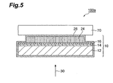
- Fig. 5 is a view showing another example of radiation image sensor including the scintillator panel in accordance with the first embodiment.
- the radiation image sensor 100a shown in Fig. 5 comprises the scintillator panel 10, and an image pickup device 70 which is arranged so as to oppose the scintillator panel 10 and adapted to convert light emitted from the scintillator 24 into an electric signal.
- the scintillator 24 is arranged between the aluminum substrate 12 and image pickup device 70.
- the light-receiving surface of the image pickup device 70 is arranged on the scintillator 24 side.
- the scintillator panel 10 and image pickup device 70 may be joined together or separated from each other. When joining them, an adhesive may be used, or an optical coupling material (refractive index matching material) may be utilized so as to reduce the loss of the emitted light 32 in view of the refractive indexes of the scintillator 24 and protective film 26.
- the radiation image sensor 100a comprises the scintillator panel 10 and the image pickup device 70 adapted to convert the light 32 emitted from the scintillator 24 of the scintillator panel 10 into the electric signal. Therefore, the radiation image sensor 100a can prevent the aluminum substrate 12 from corroding.
- Fig. 6 is a sectional view schematically showing the scintillator panel in accordance with a second embodiment.
- the scintillator panel 10a shown in Fig. 6 has the same structure as that of the scintillator panel 10 except that the intermediate film 16 totally seals the aluminum substrate 12 and alumite layer 14. Therefore, the scintillator panel 10a not only exhibits the same operations and effects as those of the scintillator 10, but further improves the moisture resistance of the aluminum substrate 12, and thus can more reliably prevent the aluminum substrate 12 from corroding.
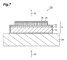
- Fig. 7 is a sectional view schematically showing the scintillator panel in accordance with a third embodiment.
- the scintillator panel 10b shown in Fig. 7 further comprises a radiation-transparent reinforcement plate 28 bonded to the aluminum substrate 12 in addition to the structure of the scintillator panel 10.
- the aluminum substrate 12 is arranged between the reinforcement plate 28 and scintillator 24.
- the reinforcement plate 28 is bonded to the aluminum substrate 12 by a double-sided adhesive tape, an adhesive, or the like, for example.
- the reinforcement plate 28 are (1) carbon fiber reinforced plastics (CFRP), (2) carbon boards (made by carbonizing and solidifying charcoal and paper), (3) carbon substrates (graphite substrates), (4) plastic substrates, (5) sandwiches of thinly formed substrates (1) to (4) mentioned above with resin foam, and the like.
- CFRP carbon fiber reinforced plastics
- the thickness of the reinforcement plate 28 is greater than the total thickness of the aluminum substrate 12 and alumite layer 14. This improves the strength of the scintillator panel 10b as a whole.
- the reinforcement plate 28 is larger than the scintillator 24 when seen in the thickness direction of the aluminum substrate 12.
- the reinforcement plate 28 hides the scintillator 24 when seen in the thickness direction of the aluminum substrate 12 from the reinforcement plate 28 side. This can prevent a shadow of the reinforcement plate 28 from being projected. In particular, this can prevent an image from becoming uneven because of the shadow of the reinforcement plate 28 when the radiation image 30 having a low energy is used.
- the scintillator 10b not only exhibits the same operations and effects as those of the scintillator panel 10, but can further improve the flatness and rigidity of the scintillator panel 10b. Therefore, the scintillator panel 10b can prevent the scintillator 24 from peeling off as the aluminum substrate 12 bends. Since the radiation image sensor 100 shown in Fig. 4 uses the scintillator panel as a single unit, it is effective to employ the scintillator panel 10b having a high rigidity.
- the reinforcement plate 28 may be bonded to the scintillator panel 10a instead of the scintillator panel 10.
- the radiation image sensors 100, 100a may employ one of the scintillator panels 10a, 10b in place of the scintillator panel 10.
- the scintillator panels 10, 10a, 10b may be free of the protective film 26.
- a stimulable phosphor (an example of a converting part adapted to convert a radiation image) may be used in place of the scintillator 24, whereby an imaging plate as the radiation image conversion panel can be made.
- the stimulable phosphor converts the radiation image into a latent image. This latent image is scanned with laser light, so as to read a visible light image.
- the visible light image is detected by a detector (photosensor such as line sensor, image sensor, and photomultiplier).
Landscapes
- Physics & Mathematics (AREA)
- Health & Medical Sciences (AREA)
- Life Sciences & Earth Sciences (AREA)
- General Physics & Mathematics (AREA)
- High Energy & Nuclear Physics (AREA)
- Molecular Biology (AREA)
- Spectroscopy & Molecular Physics (AREA)
- Chemical & Material Sciences (AREA)
- Crystallography & Structural Chemistry (AREA)
- Measurement Of Radiation (AREA)
- Conversion Of X-Rays Into Visible Images (AREA)
Applications Claiming Priority (1)
| Application Number | Priority Date | Filing Date | Title |
|---|---|---|---|
| US11/812,232 US20080311484A1 (en) | 2007-06-15 | 2007-06-15 | Radiation image conversion panel, scintillator panel, and radiation image sensor |
Publications (1)
| Publication Number | Publication Date |
|---|---|
| EP2006710A2 true EP2006710A2 (en) | 2008-12-24 |
Family
ID=39967587
Family Applications (1)
| Application Number | Title | Priority Date | Filing Date |
|---|---|---|---|
| EP08010625A Withdrawn EP2006710A2 (en) | 2007-06-15 | 2008-06-11 | Radiation image conversion panel, scintillator panel, and radiation image sensor |
Country Status (6)
| Country | Link |
|---|---|
| US (1) | US20080311484A1 (enExample) |
| EP (1) | EP2006710A2 (enExample) |
| JP (1) | JP2008309769A (enExample) |
| KR (1) | KR101026620B1 (enExample) |
| CN (1) | CN101324670A (enExample) |
| CA (1) | CA2633658A1 (enExample) |
Cited By (1)
| Publication number | Priority date | Publication date | Assignee | Title |
|---|---|---|---|---|
| FR2944879A1 (fr) * | 2009-04-28 | 2010-10-29 | Centre Nat Rech Scient | Detecteur de radiation a cristaux scintillants et procede de fabrication d'une enveloppe pour un tel detecteur. |
Families Citing this family (6)
| Publication number | Priority date | Publication date | Assignee | Title |
|---|---|---|---|---|
| JP2011137665A (ja) * | 2009-12-26 | 2011-07-14 | Canon Inc | シンチレータパネル及び放射線撮像装置とその製造方法、ならびに放射線撮像システム |
| CN101893717A (zh) * | 2010-06-24 | 2010-11-24 | 江苏康众数字医疗设备有限公司 | 闪烁体面板以及闪烁体组合板 |
| JP5498982B2 (ja) * | 2011-03-11 | 2014-05-21 | 富士フイルム株式会社 | 放射線撮影装置 |
| USD806249S1 (en) * | 2014-12-16 | 2017-12-26 | Hamamatsu Photonics K.K. | Radiation image conversion plate |
| JP6504997B2 (ja) * | 2015-11-05 | 2019-04-24 | 浜松ホトニクス株式会社 | 放射線像変換パネル、放射線像変換パネルの製造方法、放射線イメージセンサ及び放射線イメージセンサの製造方法 |
| JP6725288B2 (ja) * | 2016-03-30 | 2020-07-15 | 浜松ホトニクス株式会社 | 放射線検出器の製造方法 |
Citations (3)
| Publication number | Priority date | Publication date | Assignee | Title |
|---|---|---|---|---|
| JPH04118599A (ja) | 1990-09-10 | 1992-04-20 | Fujitsu Ltd | X線画像変換シートおよびそのシートを用いる装置 |
| US6777690B2 (en) | 1998-06-18 | 2004-08-17 | Hamamatsu Photonics K.K. | Organic film vapor deposition method and a scintillator panel |
| JP2006113007A (ja) | 2004-10-18 | 2006-04-27 | Konica Minolta Medical & Graphic Inc | 放射線画像変換パネル |
Family Cites Families (12)
| Publication number | Priority date | Publication date | Assignee | Title |
|---|---|---|---|---|
| DE3578359D1 (de) * | 1984-12-17 | 1990-07-26 | Konishiroku Photo Ind | Schirm zum speichern eines strahlungsbildes. |
| US4873708A (en) * | 1987-05-11 | 1989-10-10 | General Electric Company | Digital radiographic imaging system and method therefor |
| WO2002061459A1 (en) * | 2001-01-30 | 2002-08-08 | Hamamatsu Photonics K.K. | Scintillator panel and radiation image sensor |
| AU3678300A (en) * | 1999-04-16 | 2000-11-02 | Hamamatsu Photonics K.K. | Scintillator panel and radiation image sensor |
| JP3126715B2 (ja) * | 1999-04-16 | 2001-01-22 | 浜松ホトニクス株式会社 | シンチレータパネル及び放射線イメージセンサ |
| US7141803B2 (en) * | 2000-09-11 | 2006-11-28 | Hamamatsu Photonics K.K. | Scintillator panel, radiation image sensor and methods of producing them |
| DE20021660U1 (de) | 2000-12-20 | 2002-05-02 | Alanod Aluminium Veredlung Gmb | Verbundmaterial |
| US6652996B2 (en) * | 2002-01-31 | 2003-11-25 | Eastman Kodak Company | Radiographic phosphor panel having improved speed and sharpness |
| JP2005181220A (ja) * | 2003-12-22 | 2005-07-07 | Fuji Photo Film Co Ltd | 放射線像変換パネル |
| JP2006119124A (ja) * | 2004-09-22 | 2006-05-11 | Fuji Photo Film Co Ltd | 放射線像変換パネルおよびその製造方法 |
| US20060060792A1 (en) * | 2004-09-22 | 2006-03-23 | Fuji Photo Film Co., Ltd. | Radiographic image conversion panel and method of manufacturing the same |
| JP2006194860A (ja) * | 2004-12-16 | 2006-07-27 | Konica Minolta Medical & Graphic Inc | 放射線画像変換パネル及び放射線画像変換パネルの製造方法 |
-
2007
- 2007-06-15 US US11/812,232 patent/US20080311484A1/en not_active Abandoned
- 2007-12-19 JP JP2007327658A patent/JP2008309769A/ja active Pending
-
2008
- 2008-06-05 CA CA002633658A patent/CA2633658A1/en not_active Abandoned
- 2008-06-11 EP EP08010625A patent/EP2006710A2/en not_active Withdrawn
- 2008-06-12 KR KR1020080055237A patent/KR101026620B1/ko not_active Expired - Fee Related
- 2008-06-16 CN CNA200810109995XA patent/CN101324670A/zh active Pending
Patent Citations (3)
| Publication number | Priority date | Publication date | Assignee | Title |
|---|---|---|---|---|
| JPH04118599A (ja) | 1990-09-10 | 1992-04-20 | Fujitsu Ltd | X線画像変換シートおよびそのシートを用いる装置 |
| US6777690B2 (en) | 1998-06-18 | 2004-08-17 | Hamamatsu Photonics K.K. | Organic film vapor deposition method and a scintillator panel |
| JP2006113007A (ja) | 2004-10-18 | 2006-04-27 | Konica Minolta Medical & Graphic Inc | 放射線画像変換パネル |
Cited By (2)
| Publication number | Priority date | Publication date | Assignee | Title |
|---|---|---|---|---|
| FR2944879A1 (fr) * | 2009-04-28 | 2010-10-29 | Centre Nat Rech Scient | Detecteur de radiation a cristaux scintillants et procede de fabrication d'une enveloppe pour un tel detecteur. |
| WO2010125292A1 (fr) * | 2009-04-28 | 2010-11-04 | Centre National De La Recherche Scientifique | Detecteur de radiation a cristaux scintillants et procede de fabrication d'une enveloppe pour un tel detecteur. |
Also Published As
| Publication number | Publication date |
|---|---|
| KR101026620B1 (ko) | 2011-04-04 |
| CA2633658A1 (en) | 2008-12-15 |
| US20080311484A1 (en) | 2008-12-18 |
| CN101324670A (zh) | 2008-12-17 |
| KR20080110509A (ko) | 2008-12-18 |
| JP2008309769A (ja) | 2008-12-25 |
Similar Documents
| Publication | Publication Date | Title |
|---|---|---|
| US7812315B2 (en) | Radiation image conversion panel, scintillator panel, and radiation image sensor | |
| EP1118878B1 (en) | Scintillator panel, radiation image sensor, and method for producing the same | |
| CA2508651C (en) | Scintillator panel and radiation image sensor | |
| EP2006710A2 (en) | Radiation image conversion panel, scintillator panel, and radiation image sensor | |
| EP2012181B1 (en) | Radiation image conversion panel, scintillator panel, and radiation image sensor | |
| CN108352208A (zh) | 放射线图像变换面板、放射线图像变换面板的制造方法、放射线图像传感器及放射线图像传感器的制造方法 | |
| JP6643098B2 (ja) | 放射線検出装置、放射線検出システム、及び、放射線検出装置の製造方法 | |
| EP3062127B1 (en) | Radiation image converting panel and radiation image sensor | |
| JPWO2008117589A1 (ja) | 放射線用シンチレータパネル及び放射線画像撮影装置 | |
| JP2019049437A (ja) | 放射線検出装置及び放射線検出システム |
Legal Events
| Date | Code | Title | Description |
|---|---|---|---|
| PUAI | Public reference made under article 153(3) epc to a published international application that has entered the european phase |
Free format text: ORIGINAL CODE: 0009012 |
|
| 17P | Request for examination filed |
Effective date: 20080611 |
|
| AK | Designated contracting states |
Kind code of ref document: A2 Designated state(s): AT BE BG CH CY CZ DE DK EE ES FI FR GB GR HR HU IE IS IT LI LT LU LV MC MT NL NO PL PT RO SE SI SK TR |
|
| AX | Request for extension of the european patent |
Extension state: AL BA MK RS |
|
| STAA | Information on the status of an ep patent application or granted ep patent |
Free format text: STATUS: THE APPLICATION HAS BEEN WITHDRAWN |
|
| 18W | Application withdrawn |
Effective date: 20100208 |