EP2003459A1 - Vorrichtung zur Herstellung elektronischer Anordnungen - Google Patents
Vorrichtung zur Herstellung elektronischer Anordnungen Download PDFInfo
- Publication number
- EP2003459A1 EP2003459A1 EP07110005A EP07110005A EP2003459A1 EP 2003459 A1 EP2003459 A1 EP 2003459A1 EP 07110005 A EP07110005 A EP 07110005A EP 07110005 A EP07110005 A EP 07110005A EP 2003459 A1 EP2003459 A1 EP 2003459A1
- Authority
- EP
- European Patent Office
- Prior art keywords
- electronic apparatus
- manufacturing cell
- apparatus manufacturing
- cell
- envelope
- Prior art date
- Legal status (The legal status is an assumption and is not a legal conclusion. Google has not performed a legal analysis and makes no representation as to the accuracy of the status listed.)
- Granted
Links
Images



Classifications
-
- G—PHYSICS
- G01—MEASURING; TESTING
- G01R—MEASURING ELECTRIC VARIABLES; MEASURING MAGNETIC VARIABLES
- G01R31/00—Arrangements for testing electric properties; Arrangements for locating electric faults; Arrangements for electrical testing characterised by what is being tested not provided for elsewhere
- G01R31/01—Subjecting similar articles in turn to test, e.g. "go/no-go" tests in mass production; Testing objects at points as they pass through a testing station
Definitions
- the present disclosure generally relates to the manufacturing of electronic apparatuses. More particularly, and not by way of any limitation, the present disclosure is directed to a manufacturing cell designed to optimize space within a manufacturing facility.
- the present disclosure relates to an electronic apparatus manufacturing cell defining an electronic apparatus manufacturing cell envelope having a first side and having a second side.
- the electronic apparatus manufacturing cell comprises an infeed conveyor extending from a point outside of the electronic apparatus manufacturing cell envelope on the first side to a point inside of the envelope and a pass conveyor, extending from a point inside the electronic apparatus manufacturing cell envelope to a point outside of the electronic apparatus manufacturing cell envelope.
- the present disclosure relates to an electronic apparatus manufacturing cell defining an electronic apparatus manufacturing cell envelope having a first side and having a second side.
- the electronic apparatus manufacturing cell comprises an infeed conveyor extending from a point outside of the electronic apparatus manufacturing cell envelope on the first side to a point inside of the envelope, a pass conveyor, extending from a point inside the electronic apparatus manufacturing cell envelope to a point outside of the electronic apparatus manufacturing cell envelope and a reject conveyor, extending from a point inside the electronic apparatus manufacturing cell envelope to a point outside of the electronic apparatus manufacturing cell envelope.
- the present disclosure relates to an electronic apparatus manufacturing cell defining an electronic apparatus manufacturing cell envelope having a first side and having a second side.
- the electronic apparatus manufacturing cell comprises an infeed conveyor extending from a point outside of the electronic assembly manufacturing cell envelope on the first side to a point inside of the envelope, a pass conveyor, extending from a point inside the electronic apparatus manufacturing cell envelope to a point outside of the electronic apparatus manufacturing cell envelope and a reject conveyor, extending from a point inside the electronic apparatus manufacturing cell envelope to a point outside of the electronic apparatus manufacturing cell envelope.
- Figure 1 is a front view of an electronic apparatus manufacturing cell
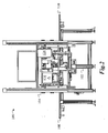
- Figure 2 is an end view of the electronic apparatus manufacturing cell
- Figure 3 is an overhead plan view of the electronic apparatus manufacturing cell
- Figure 4 is an overheard plan view of the electronic apparatus manufacturing cell showing an electronic apparatus at the entry end of the infeed conveyor;
- Figure 5 is an overheard plan view of the electronic apparatus manufacturing cell showing an electronic apparatus at the exit end of the infeed conveyor;
- Figure 6 is an overheard plan view of the electronic apparatus manufacturing cell showing an electronic apparatus at the entry end of the pass conveyor;
- Figure 7 is an overheard plan view of the electronic apparatus manufacturing cell showing an electronic apparatus at the exit end of the pass conveyor;
- Figure 8 is an overheard plan view of the electronic apparatus manufacturing cell showing an electronic apparatus at the entry end of the reject conveyor;
- Figure 9 is an overheard plan view of the electronic apparatus manufacturing cell showing an electronic apparatus at the exit end of the reject conveyor.
- Figure 10 is an overhead plan view of a set of three electronic apparatus manufacturing cells arranged in series.
- Figures 1-3 depict an electronic apparatus manufacturing cell 100 having a lower frame 102 and an upper frame 104.
- Lower frame 102 supports an infeed conveyor 106, a pass conveyor 108 and a reject conveyor 110.
- a transfer robot 112 is disposed above conveyors 106, 108, 110 and is equipped with an end effector suitable for apprehending an electronic apparatus undergoing processing and transferring it from one of conveyors 106, 108, 110 to another of conveyors 106, 108, 110.
- the determination as to the destination conveyor for an electronic apparatus undergoing processing may be made according to the results of tests performed using one or more of stations 114, 116, 118, 120.
- An electronic apparatus is brought into the electronic apparatus manufacturing cell 100 on infeed conveyor 106, processed using one or more of stations 114, 116, 118, 120, and then transferred to the appropriate outfeed conveyor according to the outcome of the processing.
- An electronic apparatus successfully passing through one or more processes performed at one or more of stations 114, 116, 118, 120 may be transferred to pass conveyor 108 and transferred to the next cell in the manufacturing facility.
- An electronic apparatus unsuccessfully completing one or more processes performed at one or more of stations 114, 116, 118, 120 may be transferred to reject conveyor 110 and transferred to the previous cell in the manufacturing facility.
- all of stations 114, 116, 118, 120 may be testing stations. In other embodiments, all of stations 114, 116, 118, 120 may be manufacturing stations. Other embodiments may incorporate a combination of manufacturing stations and testing stations, and certain stations may combine manufacturing capability and testing capability in a single station.
- an electronic apparatus may be processed at a first station 114, 116, 118, 120 and then moved to a second station 114, 116, 118, 120 or a conveyor 108, 110 within electronic apparatus manufacturing cell 100 according to the outcome of the processing at the first station 114, 116, 118, 120.
- An assembly may, for example, be initially moved to station 114, where testing is performed on the assembly. If the testing is successful, the assembly may be moved to station 116 for additional testing or other processing. If the testing is unsuccessful, the assembly may be moved to station 118 for further testing or placed on reject conveyor 110.
- stations 114, 116, 118, 120 are identical to one another, and assemblies are moved to stations 114, 116, 118, 120 according to which of stations 114, 116, 118, 120 are available at a given time.
- stations 114, 116, 118, 120 are specific to certain assembly designs, and an electronic apparatus may be moved to one or more stations 114, 116, 118, 120 within electronic apparatus manufacturing cell 100 according to the type or model of the electronic apparatus. With this capability, a variety of types of electronic apparatuses may be processed within a single apparatus.
- Operator interface panels 122 and 124 will incorporate visual displays and operator input controls such as those shown on operator interface panel 124 in figure 1 .
- Operator interface panels 122 and 124 may also incorporate audio outputs in order to capture the operator's attention when the operator is not looking at the visual display.
- Each of conveyors 106, 108, 110 has the same general construction and each of conveyors 106, 108, 110 is driven independently by a single conveyor motor 130, 132, 134, respectively.
- Each conveyor motor 130, 132, 134 powers a driving jackshaft 140, 142, 144, respectively.
- Each driving jackshaft 140, 142, 144 drives a driven jackshaft 150, 152, 154 through a drive belt 160, 162, 164.
- each pair of driving jackshafts 140, 142, 144 and driven jackshafts 150, 152, 154 impels the payload interface surface (not shown) for each conveyor 106, 108, 110.
- the payload interface surface may vary by application, but will generally be a belt, chain or cable.
- Figures 4 and 5 depict an electronic apparatus 180 entering electronic apparatus manufacturing cell 100 on infeed conveyor 106.
- the electronic apparatus 180 is disposed at the entry end of infeed conveyor 106.
- infeed conveyor 106 will draw electronic apparatus 180 into the central portion of electronic apparatus manufacturing cell 100, where it can be processed.
- Figure 5 shows the position of the electronic apparatus 180 after infeed conveyor 106 has been powered to draw electronic apparatus into the central portion of electronic apparatus manufacturing cell 100.
- electronic apparatus 180 is shown as being generally rectangular, having a longer dimension disposed perpendicularly to the direction of travel of conveyors 106, 108, 110. Alternate embodiments may be designed to accept electronic apparatuses having their longer dimension disposed parallel to the direction of conveyor travel or in some other orientation. Certain embodiments may incorporate a transfer robot 112 having the capability to reorient electronic apparatuses about one or more axes, thereby removing any necessity that the orientation of the incoming electronic apparatuses match the orientation of the stations 114, 116, 118, 120.
- electronic apparatuses such as electronic apparatus 180 may enter electronic apparatus manufacturing cell 100 oriented with their longer axis aligned to the direction of travel of the conveyors, then reoriented by transfer robot 112 to a different orientation matching the orientation of one of stations 114, 116, 118, 120. Subsequent to processing by that station, transfer robot 112 may again reorient electronic apparatus 180 to an orientation matching a different one of stations 114, 116, 118, 120 or one of conveyors 16, 108, 110.
- assemblies entering electronic apparatus manufacturing cell 100 could enter oriented with their longer axis aligned to the direction of travel of the conveyors.
- stations 114, 116, 118 120 which are oriented to interface with assemblies having their longer dimension disposed orthogonally to the direction of travel of the conveyors.
- a wide variety of possibilities will be apparent to those of skill in the art.
- the electronic apparatus 180 is drawn into the electronic apparatus manufacturing cell 100 on infeed conveyor 106, the electronic apparatus is processed using one or more of stations 114, 116, 118, 120. After the processing is complete, a determination may be made as to whether electronic apparatus 180 should be forwarded to the next manufacturing cell via pass conveyor 108 or returned to the prior manufacturing cell via reject conveyor 110. After this determination is made, transfer robot 112 is actuated to move the electronic apparatus to the appropriate outfeed conveyor 108 or 110.
- Figures 6 and 7 show an electronic apparatus 180 disposed on pass conveyor 108.
- the electronic apparatus 180 has been placed on pass conveyor 108 for transfer to the next manufacturing cell.
- Figure 7 shows the position of electronic apparatus 180 after pass conveyor 108 has been actuated in order to transfer electronic apparatus 180 to the next manufacturing cell.
- Figures 8 and 9 show an an electronic apparatus 180 disposed on pass conveyor 108.
- the electronic apparatus 180 has been placed on reject conveyor 110 for transfer to the previous manufacturing cell.
- Figure 9 shows the position of electronic apparatus 180 after reject conveyor 110 has been actuated in order to transfer electronic apparatus 180 to the previous manufacturing cell in the manufacturing line.
- conveyors 106, 108, 110 of each cell 100 extend well beyond the envelopes of a cell defined by the boundaries of frames 102 and 104.
- This design allows electronic apparatus manufacturing cell 100 to be disposed immediately adjacent to the manufacturing cells disposed before and after electronic apparatus manufacturing cell 100 without the need for intermediate conveyor units between the cells.
- Figure 10 shows a set of three processing cells 200, 202, 204 disposed immediately adjacent to one another.
- the frames 102 and 104 of cells 200, 202, 204 define rectangular envelopes 210, 212, 214, respectively.
- the conveyors 106, 108, 110 of each cell 200, 202, 204 extend through the envelope 210, 212, 214 for the cell 200, 202, 204 to the adjacent cell 200, 202, 204.
- Conveyors 106 and 110 of cell 202 for example, extend through side 220 of envelope 212 and up to envelope 210 of cell 200.
- Conveyor 108 of cell 202 extends through side 222 of envelope 212 and up to envelope 214 of cell 204. It can be seen that no additional intermediate conveyors are necessary in order to transfer electronic components between processing cells 200, 202, 204.
Landscapes
- Physics & Mathematics (AREA)
- General Physics & Mathematics (AREA)
- Container, Conveyance, Adherence, Positioning, Of Wafer (AREA)
Priority Applications (2)
| Application Number | Priority Date | Filing Date | Title |
|---|---|---|---|
| EP07110005.1A EP2003459B1 (de) | 2007-06-11 | 2007-06-11 | Vorrichtung zur Herstellung elektronischer Anordnungen |
| CA2634852A CA2634852C (en) | 2007-06-11 | 2008-06-11 | Apparatus for manufacture of electronic assemblies |
Applications Claiming Priority (1)
| Application Number | Priority Date | Filing Date | Title |
|---|---|---|---|
| EP07110005.1A EP2003459B1 (de) | 2007-06-11 | 2007-06-11 | Vorrichtung zur Herstellung elektronischer Anordnungen |
Publications (2)
| Publication Number | Publication Date |
|---|---|
| EP2003459A1 true EP2003459A1 (de) | 2008-12-17 |
| EP2003459B1 EP2003459B1 (de) | 2019-08-28 |
Family
ID=38606434
Family Applications (1)
| Application Number | Title | Priority Date | Filing Date |
|---|---|---|---|
| EP07110005.1A Active EP2003459B1 (de) | 2007-06-11 | 2007-06-11 | Vorrichtung zur Herstellung elektronischer Anordnungen |
Country Status (2)
| Country | Link |
|---|---|
| EP (1) | EP2003459B1 (de) |
| CA (1) | CA2634852C (de) |
Families Citing this family (1)
| Publication number | Priority date | Publication date | Assignee | Title |
|---|---|---|---|---|
| CN108622598A (zh) * | 2017-03-18 | 2018-10-09 | 惠州信兴荣电业塑胶有限公司 | 一种转换插头自动流水线 |
Citations (1)
| Publication number | Priority date | Publication date | Assignee | Title |
|---|---|---|---|---|
| DE19617537C1 (de) | 1996-05-02 | 1997-07-31 | Telefunken Microelectron | Meßvorrichtung zur Funktionsprüfung von Transpondern |
Family Cites Families (1)
| Publication number | Priority date | Publication date | Assignee | Title |
|---|---|---|---|---|
| US20060283688A1 (en) * | 2005-06-10 | 2006-12-21 | Applied Materials, Inc. | Substrate handling system |
-
2007
- 2007-06-11 EP EP07110005.1A patent/EP2003459B1/de active Active
-
2008
- 2008-06-11 CA CA2634852A patent/CA2634852C/en active Active
Patent Citations (1)
| Publication number | Priority date | Publication date | Assignee | Title |
|---|---|---|---|---|
| DE19617537C1 (de) | 1996-05-02 | 1997-07-31 | Telefunken Microelectron | Meßvorrichtung zur Funktionsprüfung von Transpondern |
Also Published As
| Publication number | Publication date |
|---|---|
| CA2634852A1 (en) | 2008-12-11 |
| CA2634852C (en) | 2013-10-22 |
| EP2003459B1 (de) | 2019-08-28 |
Similar Documents
| Publication | Publication Date | Title |
|---|---|---|
| CN111204587B (zh) | 一种具有mes系统与agv车的高速收放板机 | |
| CN109581135B (zh) | 产品自动测试装置及方法 | |
| CN113305569B (zh) | 一种电源风扇组装设备 | |
| KR101402364B1 (ko) | 크리센트 브라켓 자동 조립장치 | |
| CN104914117A (zh) | 一种x光检测机以及运用x光检测机的检测方法 | |
| CN215268191U (zh) | 一种连接器的自动化测试设备 | |
| CN106903069B (zh) | 一种x光检测设备 | |
| WO2000068971A3 (de) | Anlage zur bearbeitung von wafern | |
| US8132317B2 (en) | Apparatus for manufacture of electronic assemblies | |
| CA2634852C (en) | Apparatus for manufacture of electronic assemblies | |
| US20040164723A1 (en) | Indexing device in semiconductor device handler and method for operating the same | |
| CN214918263U (zh) | 自动称重扫码识别设备 | |
| CN113146242A (zh) | 马达牙箱座组装设备及其组装方法 | |
| CN100447624C (zh) | 加压脱泡炉及加压脱泡炉系统 | |
| CN114346671A (zh) | 一种推拉门窗加工生产线设备及推拉门窗加工生产方法 | |
| JP2004055697A (ja) | 基板の移載、搬送装置及び移載方法 | |
| CN220483678U (zh) | 全自动ir孔膜贴附机 | |
| KR100306303B1 (ko) | 엘씨디(lcd) 핸들러 | |
| KR100906364B1 (ko) | 작업물 공급 및 정렬 장치 | |
| KR100866831B1 (ko) | 업다운 쇼바를 갖는 평판 디스플레이 패널 검사용 반전기 | |
| CN206609940U (zh) | 一种fpc软板电测设备 | |
| KR100283781B1 (ko) | 아이씨리드 프레임 가공시스템 | |
| KR100868685B1 (ko) | 평판 디스플레이 패널 검사용 반전기 | |
| CN208385576U (zh) | 电池包自动化拆解装置 | |
| KR20100064698A (ko) | 태양 전지 모듈 제조를 위한 레이업 시스템 및 그 시스템에사용되는 정렬유닛 |
Legal Events
| Date | Code | Title | Description |
|---|---|---|---|
| PUAI | Public reference made under article 153(3) epc to a published international application that has entered the european phase |
Free format text: ORIGINAL CODE: 0009012 |
|
| 17P | Request for examination filed |
Effective date: 20070613 |
|
| AK | Designated contracting states |
Kind code of ref document: A1 Designated state(s): AT BE BG CH CY CZ DE DK EE ES FI FR GB GR HU IE IS IT LI LT LU LV MC MT NL PL PT RO SE SI SK TR |
|
| AX | Request for extension of the european patent |
Extension state: AL BA HR MK RS |
|
| AKX | Designation fees paid |
Designated state(s): AT BE BG CH CY CZ DE DK EE ES FI FR GB GR HU IE IS IT LI LT LU LV MC MT NL PL PT RO SE SI SK TR |
|
| RAP1 | Party data changed (applicant data changed or rights of an application transferred) |
Owner name: BLACKBERRY LIMITED |
|
| RAP1 | Party data changed (applicant data changed or rights of an application transferred) |
Owner name: BLACKBERRY LIMITED |
|
| 17Q | First examination report despatched |
Effective date: 20151111 |
|
| STAA | Information on the status of an ep patent application or granted ep patent |
Free format text: STATUS: EXAMINATION IS IN PROGRESS |
|
| GRAP | Despatch of communication of intention to grant a patent |
Free format text: ORIGINAL CODE: EPIDOSNIGR1 |
|
| STAA | Information on the status of an ep patent application or granted ep patent |
Free format text: STATUS: GRANT OF PATENT IS INTENDED |
|
| INTG | Intention to grant announced |
Effective date: 20190403 |
|
| GRAS | Grant fee paid |
Free format text: ORIGINAL CODE: EPIDOSNIGR3 |
|
| GRAA | (expected) grant |
Free format text: ORIGINAL CODE: 0009210 |
|
| STAA | Information on the status of an ep patent application or granted ep patent |
Free format text: STATUS: THE PATENT HAS BEEN GRANTED |
|
| AK | Designated contracting states |
Kind code of ref document: B1 Designated state(s): AT BE BG CH CY CZ DE DK EE ES FI FR GB GR HU IE IS IT LI LT LU LV MC MT NL PL PT RO SE SI SK TR |
|
| REG | Reference to a national code |
Ref country code: GB Ref legal event code: FG4D |
|
| REG | Reference to a national code |
Ref country code: CH Ref legal event code: EP |
|
| REG | Reference to a national code |
Ref country code: AT Ref legal event code: REF Ref document number: 1173059 Country of ref document: AT Kind code of ref document: T Effective date: 20190915 |
|
| REG | Reference to a national code |
Ref country code: IE Ref legal event code: FG4D |
|
| REG | Reference to a national code |
Ref country code: DE Ref legal event code: R096 Ref document number: 602007059109 Country of ref document: DE |
|
| REG | Reference to a national code |
Ref country code: NL Ref legal event code: MP Effective date: 20190828 |
|
| REG | Reference to a national code |
Ref country code: LT Ref legal event code: MG4D |
|
| PG25 | Lapsed in a contracting state [announced via postgrant information from national office to epo] |
Ref country code: FI Free format text: LAPSE BECAUSE OF FAILURE TO SUBMIT A TRANSLATION OF THE DESCRIPTION OR TO PAY THE FEE WITHIN THE PRESCRIBED TIME-LIMIT Effective date: 20190828 Ref country code: NL Free format text: LAPSE BECAUSE OF FAILURE TO SUBMIT A TRANSLATION OF THE DESCRIPTION OR TO PAY THE FEE WITHIN THE PRESCRIBED TIME-LIMIT Effective date: 20190828 Ref country code: BG Free format text: LAPSE BECAUSE OF FAILURE TO SUBMIT A TRANSLATION OF THE DESCRIPTION OR TO PAY THE FEE WITHIN THE PRESCRIBED TIME-LIMIT Effective date: 20191128 Ref country code: LT Free format text: LAPSE BECAUSE OF FAILURE TO SUBMIT A TRANSLATION OF THE DESCRIPTION OR TO PAY THE FEE WITHIN THE PRESCRIBED TIME-LIMIT Effective date: 20190828 Ref country code: SE Free format text: LAPSE BECAUSE OF FAILURE TO SUBMIT A TRANSLATION OF THE DESCRIPTION OR TO PAY THE FEE WITHIN THE PRESCRIBED TIME-LIMIT Effective date: 20190828 Ref country code: PT Free format text: LAPSE BECAUSE OF FAILURE TO SUBMIT A TRANSLATION OF THE DESCRIPTION OR TO PAY THE FEE WITHIN THE PRESCRIBED TIME-LIMIT Effective date: 20191230 |
|
| PG25 | Lapsed in a contracting state [announced via postgrant information from national office to epo] |
Ref country code: IS Free format text: LAPSE BECAUSE OF FAILURE TO SUBMIT A TRANSLATION OF THE DESCRIPTION OR TO PAY THE FEE WITHIN THE PRESCRIBED TIME-LIMIT Effective date: 20191228 Ref country code: ES Free format text: LAPSE BECAUSE OF FAILURE TO SUBMIT A TRANSLATION OF THE DESCRIPTION OR TO PAY THE FEE WITHIN THE PRESCRIBED TIME-LIMIT Effective date: 20190828 Ref country code: GR Free format text: LAPSE BECAUSE OF FAILURE TO SUBMIT A TRANSLATION OF THE DESCRIPTION OR TO PAY THE FEE WITHIN THE PRESCRIBED TIME-LIMIT Effective date: 20191129 Ref country code: LV Free format text: LAPSE BECAUSE OF FAILURE TO SUBMIT A TRANSLATION OF THE DESCRIPTION OR TO PAY THE FEE WITHIN THE PRESCRIBED TIME-LIMIT Effective date: 20190828 |
|
| REG | Reference to a national code |
Ref country code: AT Ref legal event code: MK05 Ref document number: 1173059 Country of ref document: AT Kind code of ref document: T Effective date: 20190828 |
|
| PG25 | Lapsed in a contracting state [announced via postgrant information from national office to epo] |
Ref country code: TR Free format text: LAPSE BECAUSE OF FAILURE TO SUBMIT A TRANSLATION OF THE DESCRIPTION OR TO PAY THE FEE WITHIN THE PRESCRIBED TIME-LIMIT Effective date: 20190828 |
|
| PG25 | Lapsed in a contracting state [announced via postgrant information from national office to epo] |
Ref country code: RO Free format text: LAPSE BECAUSE OF FAILURE TO SUBMIT A TRANSLATION OF THE DESCRIPTION OR TO PAY THE FEE WITHIN THE PRESCRIBED TIME-LIMIT Effective date: 20190828 Ref country code: DK Free format text: LAPSE BECAUSE OF FAILURE TO SUBMIT A TRANSLATION OF THE DESCRIPTION OR TO PAY THE FEE WITHIN THE PRESCRIBED TIME-LIMIT Effective date: 20190828 Ref country code: IT Free format text: LAPSE BECAUSE OF FAILURE TO SUBMIT A TRANSLATION OF THE DESCRIPTION OR TO PAY THE FEE WITHIN THE PRESCRIBED TIME-LIMIT Effective date: 20190828 Ref country code: AT Free format text: LAPSE BECAUSE OF FAILURE TO SUBMIT A TRANSLATION OF THE DESCRIPTION OR TO PAY THE FEE WITHIN THE PRESCRIBED TIME-LIMIT Effective date: 20190828 Ref country code: EE Free format text: LAPSE BECAUSE OF FAILURE TO SUBMIT A TRANSLATION OF THE DESCRIPTION OR TO PAY THE FEE WITHIN THE PRESCRIBED TIME-LIMIT Effective date: 20190828 Ref country code: PL Free format text: LAPSE BECAUSE OF FAILURE TO SUBMIT A TRANSLATION OF THE DESCRIPTION OR TO PAY THE FEE WITHIN THE PRESCRIBED TIME-LIMIT Effective date: 20190828 |
|
| PG25 | Lapsed in a contracting state [announced via postgrant information from national office to epo] |
Ref country code: IS Free format text: LAPSE BECAUSE OF FAILURE TO SUBMIT A TRANSLATION OF THE DESCRIPTION OR TO PAY THE FEE WITHIN THE PRESCRIBED TIME-LIMIT Effective date: 20200224 Ref country code: SK Free format text: LAPSE BECAUSE OF FAILURE TO SUBMIT A TRANSLATION OF THE DESCRIPTION OR TO PAY THE FEE WITHIN THE PRESCRIBED TIME-LIMIT Effective date: 20190828 Ref country code: CZ Free format text: LAPSE BECAUSE OF FAILURE TO SUBMIT A TRANSLATION OF THE DESCRIPTION OR TO PAY THE FEE WITHIN THE PRESCRIBED TIME-LIMIT Effective date: 20190828 |
|
| REG | Reference to a national code |
Ref country code: DE Ref legal event code: R097 Ref document number: 602007059109 Country of ref document: DE |
|
| PLBE | No opposition filed within time limit |
Free format text: ORIGINAL CODE: 0009261 |
|
| STAA | Information on the status of an ep patent application or granted ep patent |
Free format text: STATUS: NO OPPOSITION FILED WITHIN TIME LIMIT |
|
| PG2D | Information on lapse in contracting state deleted |
Ref country code: IS |
|
| 26N | No opposition filed |
Effective date: 20200603 |
|
| PG25 | Lapsed in a contracting state [announced via postgrant information from national office to epo] |
Ref country code: SI Free format text: LAPSE BECAUSE OF FAILURE TO SUBMIT A TRANSLATION OF THE DESCRIPTION OR TO PAY THE FEE WITHIN THE PRESCRIBED TIME-LIMIT Effective date: 20190828 |
|
| PG25 | Lapsed in a contracting state [announced via postgrant information from national office to epo] |
Ref country code: MC Free format text: LAPSE BECAUSE OF FAILURE TO SUBMIT A TRANSLATION OF THE DESCRIPTION OR TO PAY THE FEE WITHIN THE PRESCRIBED TIME-LIMIT Effective date: 20190828 |
|
| REG | Reference to a national code |
Ref country code: CH Ref legal event code: PL |
|
| PG25 | Lapsed in a contracting state [announced via postgrant information from national office to epo] |
Ref country code: LU Free format text: LAPSE BECAUSE OF NON-PAYMENT OF DUE FEES Effective date: 20200611 |
|
| REG | Reference to a national code |
Ref country code: BE Ref legal event code: MM Effective date: 20200630 |
|
| PG25 | Lapsed in a contracting state [announced via postgrant information from national office to epo] |
Ref country code: LI Free format text: LAPSE BECAUSE OF NON-PAYMENT OF DUE FEES Effective date: 20200630 Ref country code: IE Free format text: LAPSE BECAUSE OF NON-PAYMENT OF DUE FEES Effective date: 20200611 Ref country code: CH Free format text: LAPSE BECAUSE OF NON-PAYMENT OF DUE FEES Effective date: 20200630 |
|
| PG25 | Lapsed in a contracting state [announced via postgrant information from national office to epo] |
Ref country code: BE Free format text: LAPSE BECAUSE OF NON-PAYMENT OF DUE FEES Effective date: 20200630 |
|
| PG25 | Lapsed in a contracting state [announced via postgrant information from national office to epo] |
Ref country code: MT Free format text: LAPSE BECAUSE OF FAILURE TO SUBMIT A TRANSLATION OF THE DESCRIPTION OR TO PAY THE FEE WITHIN THE PRESCRIBED TIME-LIMIT Effective date: 20190828 Ref country code: CY Free format text: LAPSE BECAUSE OF FAILURE TO SUBMIT A TRANSLATION OF THE DESCRIPTION OR TO PAY THE FEE WITHIN THE PRESCRIBED TIME-LIMIT Effective date: 20190828 |
|
| REG | Reference to a national code |
Ref country code: DE Ref legal event code: R082 Ref document number: 602007059109 Country of ref document: DE Ref country code: DE Ref legal event code: R081 Ref document number: 602007059109 Country of ref document: DE Owner name: MALIKIE INNOVATIONS LTD., IE Free format text: FORMER OWNER: BLACKBERRY LIMITED, WATERLOO, ONTARIO, CA |
|
| PGFP | Annual fee paid to national office [announced via postgrant information from national office to epo] |
Ref country code: DE Payment date: 20250626 Year of fee payment: 19 |
|
| PGFP | Annual fee paid to national office [announced via postgrant information from national office to epo] |
Ref country code: GB Payment date: 20250617 Year of fee payment: 19 |
|
| PGFP | Annual fee paid to national office [announced via postgrant information from national office to epo] |
Ref country code: FR Payment date: 20250624 Year of fee payment: 19 |