EP1998363A2 - Frequency Doubling Using Spacer Mask - Google Patents
Frequency Doubling Using Spacer Mask Download PDFInfo
- Publication number
- EP1998363A2 EP1998363A2 EP08157222A EP08157222A EP1998363A2 EP 1998363 A2 EP1998363 A2 EP 1998363A2 EP 08157222 A EP08157222 A EP 08157222A EP 08157222 A EP08157222 A EP 08157222A EP 1998363 A2 EP1998363 A2 EP 1998363A2
- Authority
- EP
- European Patent Office
- Prior art keywords
- mask
- spacer
- layer
- sacrificial
- comprised
- Prior art date
- Legal status (The legal status is an assumption and is not a legal conclusion. Google has not performed a legal analysis and makes no representation as to the accuracy of the status listed.)
- Withdrawn
Links
Images




Classifications
-
- H—ELECTRICITY
- H10—SEMICONDUCTOR DEVICES; ELECTRIC SOLID-STATE DEVICES NOT OTHERWISE PROVIDED FOR
- H10P—GENERIC PROCESSES OR APPARATUS FOR THE MANUFACTURE OR TREATMENT OF DEVICES COVERED BY CLASS H10
- H10P50/00—Etching of wafers, substrates or parts of devices
- H10P50/69—Etching of wafers, substrates or parts of devices using masks for semiconductor materials
- H10P50/691—Etching of wafers, substrates or parts of devices using masks for semiconductor materials for Group V materials or Group III-V materials
- H10P50/692—Etching of wafers, substrates or parts of devices using masks for semiconductor materials for Group V materials or Group III-V materials characterised by their composition, e.g. multilayer masks or materials
-
- H—ELECTRICITY
- H10—SEMICONDUCTOR DEVICES; ELECTRIC SOLID-STATE DEVICES NOT OTHERWISE PROVIDED FOR
- H10P—GENERIC PROCESSES OR APPARATUS FOR THE MANUFACTURE OR TREATMENT OF DEVICES COVERED BY CLASS H10
- H10P50/00—Etching of wafers, substrates or parts of devices
- H10P50/69—Etching of wafers, substrates or parts of devices using masks for semiconductor materials
- H10P50/691—Etching of wafers, substrates or parts of devices using masks for semiconductor materials for Group V materials or Group III-V materials
- H10P50/693—Etching of wafers, substrates or parts of devices using masks for semiconductor materials for Group V materials or Group III-V materials characterised by their size, orientation, disposition, behaviour or shape, in horizontal or vertical plane
- H10P50/695—Etching of wafers, substrates or parts of devices using masks for semiconductor materials for Group V materials or Group III-V materials characterised by their size, orientation, disposition, behaviour or shape, in horizontal or vertical plane characterised by the process involved to create the mask, e.g. lift-off masks or sidewalls or to modify the mask
-
- H—ELECTRICITY
- H10—SEMICONDUCTOR DEVICES; ELECTRIC SOLID-STATE DEVICES NOT OTHERWISE PROVIDED FOR
- H10P—GENERIC PROCESSES OR APPARATUS FOR THE MANUFACTURE OR TREATMENT OF DEVICES COVERED BY CLASS H10
- H10P50/00—Etching of wafers, substrates or parts of devices
- H10P50/69—Etching of wafers, substrates or parts of devices using masks for semiconductor materials
- H10P50/691—Etching of wafers, substrates or parts of devices using masks for semiconductor materials for Group V materials or Group III-V materials
- H10P50/693—Etching of wafers, substrates or parts of devices using masks for semiconductor materials for Group V materials or Group III-V materials characterised by their size, orientation, disposition, behaviour or shape, in horizontal or vertical plane
- H10P50/696—Process specially adapted to improve the resolution of the mask
-
- H—ELECTRICITY
- H10—SEMICONDUCTOR DEVICES; ELECTRIC SOLID-STATE DEVICES NOT OTHERWISE PROVIDED FOR
- H10P—GENERIC PROCESSES OR APPARATUS FOR THE MANUFACTURE OR TREATMENT OF DEVICES COVERED BY CLASS H10
- H10P50/00—Etching of wafers, substrates or parts of devices
- H10P50/71—Etching of wafers, substrates or parts of devices using masks for conductive or resistive materials
-
- H—ELECTRICITY
- H10—SEMICONDUCTOR DEVICES; ELECTRIC SOLID-STATE DEVICES NOT OTHERWISE PROVIDED FOR
- H10P—GENERIC PROCESSES OR APPARATUS FOR THE MANUFACTURE OR TREATMENT OF DEVICES COVERED BY CLASS H10
- H10P50/00—Etching of wafers, substrates or parts of devices
- H10P50/73—Etching of wafers, substrates or parts of devices using masks for insulating materials
-
- H—ELECTRICITY
- H10—SEMICONDUCTOR DEVICES; ELECTRIC SOLID-STATE DEVICES NOT OTHERWISE PROVIDED FOR
- H10P—GENERIC PROCESSES OR APPARATUS FOR THE MANUFACTURE OR TREATMENT OF DEVICES COVERED BY CLASS H10
- H10P76/00—Manufacture or treatment of masks on semiconductor bodies, e.g. by lithography or photolithography
- H10P76/40—Manufacture or treatment of masks on semiconductor bodies, e.g. by lithography or photolithography of masks comprising inorganic materials
- H10P76/405—Manufacture or treatment of masks on semiconductor bodies, e.g. by lithography or photolithography of masks comprising inorganic materials characterised by their composition, e.g. multilayer masks
-
- H—ELECTRICITY
- H10—SEMICONDUCTOR DEVICES; ELECTRIC SOLID-STATE DEVICES NOT OTHERWISE PROVIDED FOR
- H10P—GENERIC PROCESSES OR APPARATUS FOR THE MANUFACTURE OR TREATMENT OF DEVICES COVERED BY CLASS H10
- H10P76/00—Manufacture or treatment of masks on semiconductor bodies, e.g. by lithography or photolithography
- H10P76/40—Manufacture or treatment of masks on semiconductor bodies, e.g. by lithography or photolithography of masks comprising inorganic materials
- H10P76/408—Manufacture or treatment of masks on semiconductor bodies, e.g. by lithography or photolithography of masks comprising inorganic materials characterised by their sizes, orientations, dispositions, behaviours or shapes
- H10P76/4085—Manufacture or treatment of masks on semiconductor bodies, e.g. by lithography or photolithography of masks comprising inorganic materials characterised by their sizes, orientations, dispositions, behaviours or shapes characterised by the processes involved to create the masks
-
- H—ELECTRICITY
- H10—SEMICONDUCTOR DEVICES; ELECTRIC SOLID-STATE DEVICES NOT OTHERWISE PROVIDED FOR
- H10P—GENERIC PROCESSES OR APPARATUS FOR THE MANUFACTURE OR TREATMENT OF DEVICES COVERED BY CLASS H10
- H10P76/00—Manufacture or treatment of masks on semiconductor bodies, e.g. by lithography or photolithography
- H10P76/40—Manufacture or treatment of masks on semiconductor bodies, e.g. by lithography or photolithography of masks comprising inorganic materials
- H10P76/408—Manufacture or treatment of masks on semiconductor bodies, e.g. by lithography or photolithography of masks comprising inorganic materials characterised by their sizes, orientations, dispositions, behaviours or shapes
- H10P76/4088—Processes for improving the resolution of the masks
Definitions
- Embodiments of the present invention pertain to the field of Semiconductor Processing. More particularly, embodiments of the present invention relate to a method of fabricating a semiconductor device.
- FIGS. 1A-C illustrate cross-sectional views representing a conventional semiconductor lithographic process, in accordance with the prior art.
- a photoresist layer 104 is provided above a semiconductor stack 102.
- a mask or reticle 106 is positioned above the photoresist layer 104.
- a lithographic process includes exposure of the photoresist layer 104 to light (hv) having a particular wavelength, as indicated by the arrows in Figure 1A .
- the photoresist layer 104 is subsequently developed to provide the patterned photoresist layer 108 above the semiconductor stack 102. That is, the portions of the photoresist layer 104 that were exposed to light are now removed.
- each feature of the patterned photoresist layer 108 is depicted by the width 'x.'
- the spacing between each feature is depicted by the spacing 'y.'
- the critical dimension (i.e. the width 'x') of a feature may be reduced to form the patterned photoresist layer 110 above the semiconductor stack 102.
- the critical dimension may be shrunk by over-exposing the photoresist layer 104 during the lithographic operation depicted in Figure 1A or by subsequently trimming the patterned photoresist layer 108 from Figure 1B .
- this reduction in critical dimension comes at the expense of an increased spacing between features, as depicted by spacing 'y' in Figure 1C . That is, there may be a trade-off between the smallest achievable dimension of each of the features from the patterned photoresist layer 110 and the spacing between each feature.
- Figures 1A-C illustrate cross-sectional views representing a conventional semiconductor lithographic process, in accordance with the prior art.
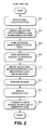
- Figure 2 illustrates an exemplary method of a spacer mask fabrication process, in accordance with an embodiment of the present invention.
- Figures 3A-H illustrate cross-sectional and top-down views representing a series of processes from the flowchart of Figure 2 as applied to a semiconductor stack, in accordance with an embodiment of the present invention.
- Figures 4A-B illustrate top-down views of an exemplary method of a spacer mask fabrication process, in accordance with an embodiment of the present invention.
- Figures 5A-D illustrate cross-sectional views of an exemplary method of a spacer mask fabrication process, in accordance with an embodiment of the present invention.
- Figures 6A-B illustrate top-down views of an exemplary method of a spacer mask fabrication process, in accordance with an embodiment of the present invention.
- a method for fabricating a semiconductor mask is provided.
- a semiconductor stack having a sacrificial mask and a spacer mask may first be provided.
- the sacrificial mask comprises a series of lines and the spacer mask has spacer lines adjacent to the sidewalls of the series of lines.
- the spacer mask is then cropped to provide a cropped spacer mask and the sacrificial mask is removed subsequent to the cropping of the spacer mask.
- the spacer mask is formed by first depositing a spacer layer above the semiconductor stack and conformal with the sacrificial mask.
- the spacer layer is etched to provide the spacer mask having spacer lines adjacent to the sidewalls of the series of lines of the sacrificial mask and to expose the top surface of the sacrificial mask.
- a photoresist layer is then deposited and patterned above the spacer mask to expose a portion of the spacer mask.
- the exposed portion of the spacer mask is etched to crop the spacer mask. Finally, the sacrificial mask is removed, leaving only the cropped spacer mask.
- the frequency of a lithographic pattern may be doubled by fabricating a spacer mask.
- a spacer mask is fabricated having spacer lines formed adjacent to the sidewalls of a lithographically patterned sacrificial mask. As such, for every line in the sacrificial mask, two spacer lines of the spacer mask are generated.
- a semiconductor patterning mask providing substantially the same critical dimension for each line, or the same feature width, but having double the density of lines in a particular region may thus be fabricated upon removal of the sacrificial mask.
- the pitch of the sacrificial mask is selected to be 4 in order to ultimately provide a spacer mask having a pitch of 2.
- a spacer mask In order to provide spacer lines that do not wrap around the ends of the lines of the sacrificial mask, the spacer mask may need to be cropped. Damage to the spacer mask during a cropping operation may be prevented by retaining the sacrificial mask until the spacer mask has been cropped.
- a spacer mask comprises spacer regions which are directly adjacent to the sidewalls of the lines in a sacrificial mask, including around the ends of each line. Each pair of spacer regions of the spacer mask associated with each line of the sacrificial mask is connected. It may be desirable to generate lines in the spacer mask that are discontinuous with one another.
- the portions of the spacer mask that wrap around the ends of the lines in the sacrificial mask are cropped in a patterning/etch process.
- the spacer mask may not have sufficient integrity to endure the patterning/etch process.
- the sacrificial mask is retained during the cropping process in order to provide structural support to the spacer mask throughout the process.
- the sacrificial mask may be removed to provide only the cropped spacer mask.
- the image of the cropped spacer mask is subsequently transferred to a semiconductor stack.
- FIG. 2 comprises a flowchart 200 representing an exemplary method of a spacer mask fabrication process, in accordance with an embodiment of the present invention.
- Figures 3A-H illustrate cross-sectional and top-down views accompanying the exemplary method from flowchart 200 as applied to a semiconductor stack, in accordance with an embodiment of the present invention.
- a patterned photoresist layer 302 is provided above a semiconductor stack 300.
- the semiconductor stack 300 is comprised of a first mask stack 304 and a second mask stack 306 above a semiconductor layer 308.
- the patterned photoresist layer 302 may be comprised of any material suitable for use in a lithographic process.
- the patterned photoresist layer 302 may be formed by first masking a blanket layer of photoresist material and then exposing it to a light source. The patterned photoresist layer 302 may then be formed by developing the blanket photoresist layer. In an embodiment, the portions of the photoresist layer exposed to the light source are removed upon developing the photoresist layer.
- the patterned photoresist layer 302 is comprised of a positive photoresist material in the present embodiment.
- the patterned photoresist layer 302 is comprised of a positive photoresist material selected from the group consisting of a 248nm resist, a 193nm resist, a 157nm resist and a phenolic resin matrix with a diazonaphthoquinone sensitizer.
- the portions of the photoresist layer exposed to the light source are retained upon developing the photoresist layer.
- the patterned photoresist layer 302 is comprised of a negative photoresist material in the present embodiment.
- the patterned photoresist layer 302 is comprised of a negative photoresist material selected from the group consisting of poly-cis-isoprene and poly-vinyl-cinnamate.
- the patterned photoresist layer 302 may have any dimensions suitable for a spacer mask fabrication process.
- the width 'x' of each feature of the patterned photoresist layer 302 is selected to substantially correlate with the desired critical dimension of a semiconductor device feature, e.g. the width of a space that defines a gate electrode.
- the width 'x' is in the range of 10 - 100 nanometers.
- the spacing between lines 'y' may be selected to optimize a frequency doubling scheme.
- a subsequently fabricated spacer mask is targeted such that the width of the spacer lines of the spacer mask are substantially the same as the width 'x' of each feature of the patterned photoresist layer 302. Furthermore, the spacing between subsequently formed spacer lines is targeted to be substantially equal to the width of each spacer region. Thus, in one embodiment, because the frequency will ultimately be doubled, the spacing 'y' between each feature in the patterned photoresist 302 is approximately equal to 3 times the value 'x,' as depicted in Figure 3A .
- the pitch of the patterned photoresist layer 302 is selected to be approximately 4 in order to ultimately provide a spacer mask with spacer lines having a pitch of approximately 2.
- 193 nm lithography is used to generate the patterned photoresist layer 302 having a feature width of approximately 45 nanometers and a spacing between features of approximately 135 nanometers.
- the approximate 3:1 spacing:width ratio for the features of the patterned photoresist layer 302 may be achieved by over-exposing a positive photoresist layer at the exposure operation or by trimming a photoresist layer subsequent to a lithographic/development process.
- the patterned photoresist 302 is comprised of 193 nm positive photoresist that was trimmed post development by using a plasma etch chemistry.
- the ideal width of each feature in the patterned photoresist layer 302 is 1 ⁇ 4 the pitch of the patterned photoresist layer 302, the initial targeted width may be required to be slightly thicker to compensate for the etch process used to pattern the first mask stack 304.
- the initial width of each line in the patterned photoresist layer 302 is targeted to be between 0.281 and 0.312 times the pitch.
- the image of the patterned photoresist layer 302 is transferred to the first mask stack 304 by an etch process to form a sacrificial mask 310.
- the etch process used to transfer the image may be any process suitable to transfer substantially the same image from the patterned photoresist layer 302 to the first mask stack 304.
- the first mask stack 304 and, hence, the sacrificial mask 310 may be comprised of any material or combination of materials suitable to act as a sacrificial mask in a spacer mask fabrication process.
- the first mask stack 304 is comprised of a single material, as indicated by the single shading depicted in Figure 3A .
- the composition and thickness of first mask stack 304 comprised of a single material may be suitable for etching with an etch process that is substantially non-impactful to the patterned photoresist layer 302.
- the dimensions and etch characteristics of the first mask stack 304 comprised of a single material are selected to be amenable to patterning during which the patterned photoresist layer 302 is retained substantially intact.
- the patterned photoresist layer 302 is comprised of a carbon-based material and the first mask stack 304 is comprised of a material selected from the group consisting of silicon nitride, silicon oxide and amorphous or polycrystalline silicon.
- the first mask stack 304 is comprised substantially of silicon nitride and the etch process used to form the sacrificial mask 310 utilizes gases selected from the group consisting of CH 2 F 2 and CHF 3 .
- the first mask stack 304 is comprised substantially of silicon oxide and the etch process used to form the sacrificial mask 310 utilizes gases selected from the group consisting of C 4 F 8 and CHF 3 .
- the first mask stack 304 is comprised substantially of amorphous or polycrystalline silicon and the etch process used to form the sacrificial mask 310 utilizes gases selected from the group consisting of Cl 2 and HBr.
- the thickness of the first mask stack 304 comprised of a single material is selected to optimize the subsequent formation of a spacer mask in a frequency doubling scheme.
- the thickness of the first mask stack 304 may be sufficiently small to prevent spacer mask line-collapse of a subsequently formed spacer mask and sufficiently large to enable critical dimension control of the spacer mask lines.
- the thickness of the first mask stack 304 comprised of a single material is in the range of 4.06 - 5.625 times the targeted line width of the sacrificial mask 310.
- the first mask stack 304 is comprised of a first hardmask layer 304A above a first mask layer 304B, as indicated by the two layers depicted in Figure 3A .
- the sacrificial mask 310 is comprised of a sacrificial hardmask portion 310A above a sacrificial mask portion 310B, as depicted in Figure 3B .
- the first hardmask layer 304A and the first mask layer 304B are patterned with the image of the patterned photoresist layer 302 in two distinct etch operations.
- the first hardmask layer 304A may be comprised of any material suitable for etching with an etch process that is substantially non-impactful to the patterned photoresist layer 302.
- the dimensions and etch characteristics of the first hardmask layer 304A are selected to be amenable to a patterning process during which the patterned photoresist layer 302 is retained substantially intact.
- the first mask layer 304B (which underlies the first hardmask layer 304A) is comprised of a material with etch characteristics similar to the etch characteristics of the patterned photoresist layer 302.
- the first hardmask layer 304A is used to preserve the image from the patterned photoresist layer 302 during the subsequent etch of the first mask layer 304B.
- the patterned photoresist layer 302 and the first mask layer 304B are comprised of carbon-based materials and the first hardmask layer 304A is comprised of a material selected from the group consisting of silicon nitride, silicon oxide and amorphous or polycrystalline silicon.
- the first hardmask layer 304A is comprised substantially of silicon nitride and the etch process used to pattern the first hardmask layer 304A selective to the patterned photoresist layer 302 and the first mask layer 304B utilizes gases selected from the group consisting of CH 2 F 2 and CHF 3 .
- the first hardmask layer 304A is comprised substantially of silicon oxide and the etch process used to pattern the first hardmask layer 304A selective to the patterned photoresist layer 302 and the first mask layer 304B utilizes gases selected from the group consisting of C 4 F 8 and CHF 3 .
- the first hardmask layer 304A is comprised substantially of amorphous or polycrystalline silicon and the etch process used to pattern the first hardmask layer 304A selective to the patterned photoresist layer 302 and the first mask layer 304B utilizes gases selected from the group consisting of Cl 2 and HBr.
- the thickness of the first hardmask layer 304A may be sufficiently small to enable highly selective etching relative to the patterned photoresist layer 302 and sufficiently large to avoid pinholes that may undesirably expose the first mask layer 304B. In one embodiment, the thickness of the first hardmask layer 304A is in the range of 20 - 50 nanometers.
- the first mask layer 304B may be comprised of any material suitable to withstand a controlled etch process and a subsequent spacer mask formation process.
- the first mask layer 304B has similar etch characteristics to the patterned photoresist layer 302.
- the thicknesses of the patterned photoresist layer 302 and the first mask layer 304B are selected such that all portions of the patterned photoresist layer 302 remaining subsequent to the etch of the first hardmask layer 304A are removed during the etch of the first mask layer 304B.
- both the patterned photoresist layer 302 and the first mask layer 304B are comprised substantially of carbon atoms.
- the first mask layer 304B is comprised of a mixture of sp 3 (diamond-like)-, sp 2 (graphitic)- and sp 1 (pyrolitic)-hybridized carbon atoms formed from a chemical vapor deposition process using hydrocarbon precursor molecules.
- Such a film may be known in the art as an amorphous carbon film or Advanced Patterning Film TM (APF).
- first mask layer 304B is comprised of such an amorphous carbon film and is etched by using gases selected from the group consisting of the combination of O 2 and N 2 or the combination of CH 4 and N 2 and O 2 .
- substantially all of the patterned photoresist layer 302 is removed in the same etch operation as that used to pattern the first mask layer 304B.
- the thickness of the first mask layer 304B may be sufficiently small to prevent spacer mask line-collapse of a subsequently formed spacer mask and sufficiently large to enable critical dimension control of the spacer mask lines.
- the total thickness of the first mask stack 304 comprised of the first hardmask layer 304A and the first mask layer 304B is in the range of 4.06 - 5.625 times the targeted line width of the sacrificial mask 310.
- the first mask stack 304 (shown in Figure 3A ) is patterned to form the sacrificial mask 310 selective to the second mask stack 306.
- the second mask stack 306 is comprised of a second hardmask layer 306A above a second mask layer 306B, as depicted in Figure 3B .
- the second hardmask layer 306A may have any properties suitable to protect the second mask layer 306B from the etch process used to form the sacrificial mask 310.
- the first mask stack 304 is comprised of a single material and is etched selective to the second hardmask layer 306A.
- the first mask stack 304 is comprised of silicon nitride and the second hardmask layer 306A is comprised of a material selected from the group consisting of silicon oxide and amorphous or polycrystalline silicon.
- the first mask stack 304 is comprised of silicon oxide and the second hardmask layer 306A is comprised of a material selected from the group consisting of silicon nitride and amorphous or polycrystalline silicon.
- the first mask stack 304 is comprised of amorphous or polycrystalline silicon and the second hardmask layer 306A is comprised of a material selected from the group consisting of silicon nitride and silicon oxide.
- the first mask stack 304 is comprised of a first hardmask layer 304A and a first mask layer 304B.
- the first mask layer 304B is comprised of an amorphous carbon film etched by gases selected from the group consisting of the combination of O 2 and N 2 or the combination of CH 4 and N 2 and O 2 and the second hardmask layer 306A is comprised of a material selected from the group consisting of silicon nitride, silicon oxide and amorphous or polycrystalline silicon.
- the thickness of the second hardmask layer 306A may be sufficiently small to enable subsequent highly selective etching relative to the second mask layer 306B and sufficiently large to avoid pinholes that may undesirably expose the second mask layer 306B to the etch process applied to the first mask stack 304. In one embodiment, the thickness of the second hardmask layer 306A is in the range of 15 - 40 nanometers.
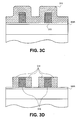
- a spacer layer 312 is deposited conformal over the sacrificial mask 310 and above the second hardmask layer 306A.
- the spacer layer 312 is the source of material for what will ultimately become a spacer mask for use in a frequency doubling scheme.
- the spacer layer 312 may be comprised of any material suitable to form a reliable mask for use in a subsequent etch process.
- the spacer layer 312 is comprised of a material selected from the group consisting of silicon nitride, silicon oxide and amorphous or polycrystalline silicon.
- the spacer layer 312 may be deposited by any process suitable to provide a conformal layer on the sidewalls of the sacrificial mask 310, as depicted in Figure 3C .
- the spacer layer 312 is deposited by a chemical vapor deposition (CVD) technique selected from the group consisting of molecular-organic CVD, low-pressure CVD and plasma-enhanced CVD.
- CVD chemical vapor deposition
- the thickness of the spacer layer 312 may be selected to determine the width of the features in a subsequently formed spacer mask.
- the thickness of the spacer layer 312 is substantially the same as the width of the features of the sacrificial mask 310, as depicted in Figure 3C .
- the initial targeted width may be required to be slightly thicker to compensate for the etch process used to pattern the spacer layer 312.
- the thickness of the spacer layer 312 is approximately 1.06 times the width of the features of the sacrificial mask 310, i.e. 1.06 times the desired feature width of the lines in a subsequently formed spacer mask.
- the spacer layer 312 is etched to provide the spacer mask 314 and to expose the top surfaces of the sacrificial mask 310 and the second hardmask layer 306A.
- the lines of the spacer mask 314 are conformal with the sidewalls of the features of the sacrificial mask 310. Thus, there are two lines from the spacer mask 314 for every line of the sacrificial mask 310, as depicted in Figure 3D .
- the spacer layer 312 may be etched by any process suitable to provide well-controlled dimensions, for instance, to maintain a width of critical dimension of the sacrificial mask 310.
- the spacer layer 312 is etched until the lines of the spacer mask 314 are substantially the same height as the features of the sacrificial mask 310, as depicted in Figure 3D .
- the lines of the spacer mask 314 are recessed slightly below the top surface of the features of the sacrificial mask 310 in order to ensure that the continuity of the spacer layer 312 is broken above and between the lines of the spacer mask 314.
- the spacer layer 312 may be etched such that the spacer lines of the spacer mask 314 retain a substantial portion of the original thickness of the spacer layer 312.
- the width of the top surface of each line of the spacer mask 314 is substantially the same as the width at the interface of the spacer mask 314 and the second hardmask layer 306A, as depicted in Figure 3D .
- the spacer layer 312 may also be etched to form the spacer mask 314 (e.g., Figure 3D ) with high etch selectivity to the sacrificial mask 310 and the second hardmask layer 306A.
- the sacrificial mask 310 is a single layer mask and the desired etch selectivity is with respect to the single layer.
- the sacrificial mask 310 is a stacked layer and the desired etch selectivity is with respect to a sacrificial hardmask portion, or with respect to the material of the first hardmask layer 304A.
- the spacer layer 312 and the spacer mask 314 is comprised of a material different than the materials of the top portion of the sacrificial mask 310 and the second hardmask layer 306A.
- the top portion of the sacrificial mask 310 is comprised of silicon nitride
- the second hardmask layer 306A is comprised of silicon oxide
- the spacer layer 312 is comprised of amorphous or polycrystalline silicon and is etched to form the spacer mask 314 with a dry etch process using a plasma generated from the gases Cl 2 or HBr.
- the top portion of the sacrificial mask 310 is comprised of silicon oxide
- the second hardmask layer 306A is comprised of silicon nitride
- the spacer layer 312 is comprised of amorphous or polycrystalline silicon and is etched to form the spacer mask 314 with a dry etch process using a plasma generated from the combination of the gases Cl 2 and HBr.
- the top portion of the sacrificial mask 310 is comprised of amorphous or polycrystalline silicon
- the second hardmask layer 306A is comprised of silicon nitride
- the spacer layer 312 is comprised of silicon oxide and is etched to form the spacer mask 314 with a dry etch process using a plasma generated from the gas C 4 F 8
- the top portion of the sacrificial mask 310 is comprised of amorphous or polycrystalline silicon
- the second hardmask layer 306A is comprised of silicon oxide
- the spacer layer 312 is comprised of silicon nitride and is etched to form the spacer mask 314 with a dry etch process using a plasma generated from the gas CH 2 F 2 .
- the top portion of the sacrificial mask 310 is comprised of silicon oxide
- the second hardmask layer 306A is comprised of amorphous or polycrystalline silicon
- the spacer layer 312 is comprised of silicon nitride and is etched to form the spacer mask 314 with a dry etch process using a plasma generated from the combination of the gases CHF 3 and CH 2 F 2 .
- the top portion of the sacrificial mask 310 is comprised of silicon nitride
- the second hardmask layer 306A is comprised of amorphous or polycrystalline silicon
- the spacer layer 312 is comprised of silicon oxide and is etched to form the spacer mask 314 with a dry etch process using a plasma generated from the gas CHF 3 .
- the etch process used to form the spacer mask 314 is end-pointed upon exposure of the top surfaces of the sacrificial mask 310 and the second hardmask layer 306A.
- a slight over-etch is applied following the end-point detection to ensure that the lines of the spacer mask 314 are discontinuous from feature to feature (e.g. line-to-line) of the sacrificial mask 310.
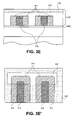
- a photoresist stack 320 is deposited above the spacer mask 314 and the exposed portions of the sacrificial mask 310 and the second hardmask layer 306A.
- the photoresist stack 320 is typically deposited before the spacer mask 314.
- the spacer lines from the spacer mask 314 were made discontinuous between neighboring lines of the sacrificial mask 310 such as those described in Figure 3D .
- spacer lines of the spacer mask 314 associated with the same line from the sacrificial mask 310 remain continuous around the ends of each of the lines of the sacrificial mask 310, as depicted by end-portions 316 of the spacer mask 314 illustrated in the top-down view of Figure 3E' . It may be desirable to break this continuity between pairs of spacer lines for subsequent semiconductor device manufacture.
- the end- portions 316 are exposed by the window 330 upon patterning the photoresist stack 320, as depicted in Figure 3E' .
- a photoresist stack 320 may have a photoresist layer 324 comprised of any material described in association with the patterned photoresist layer 302 from Figure 3A . Additionally, the photoresist stack 320 may comprise a bottom-anti-reflective-coating (BARC) layer 322 in between the photoresist layer 324 and the spacer mask 314 in order to provide a flat surface for the photoresist layer 324, as depicted in Figure 3E .
- the lithographic process used to pattern the photoresist stack 320 incorporates exposure and development of a photoresist layer 324 having a substantially flat bottom surface.
- the BARC layer is a spin-on glass material having an organic group.
- the photoresist stack 320 is comprised entirely of a photoresist layer.
- the photoresist stack 320 may be deposited by any process that provides a flat top surface for the photoresist stack 320.
- the photoresist stack 320 comprises the photoresist layer 324 above the BARC layer 322 and both the photoresist layer 324 and the BARC layer 322 are deposited by a spin-on process.
- the photoresist stack 320 substantially comprises a photoresist layer which is deposited by a spin-on process.
- the spin-on process used to deposit the BARC layer 322 or a photoresist layer may generate enough force to topple a thin feature or line in a spacer mask.
- the spin-on process may generate enough force to topple a stand-alone line from the spacer mask 314.
- the sacrificial mask 310 is retained throughout the spacer cropping process in order to provide structural support to the individual spacer lines from the spacer mask 314.
- no spacer lines from the spacer mask 314 are toppled in the spin-on process used to deposit the photoresist stack 320.
- the photoresist stack 320 may be patterned by any lithographic process described in association with the patterning of the patterned photoresist layer 302 from Figure 3A .
- the photoresist stack 320 is patterned to form a window 330 that exposes the end-portions 316 of the spacer mask 314.
- the size of the window 330 may be any dimension suitable to crop the spacer mask 314.
- the region 330 may expose at least the entire end-portions 316 of the spacer mask 314.
- the dimensions of the window 330 are selected to also expose a portion of the sacrificial mask 310.
- the dimensions and positioning of the window 330 in the photoresist stack 320 are selected to accommodate for any slight offset in the patterning and, hence, cropping process.
- the spacer mask 314 is cropped to form a cropped spacer mask 340.
- the spacer mask 314 may be cropped by any etch process that removes the exposed portions of the spacer mask 314. As illustrated, the end-portions 316, selective to the photoresist stack 320 and the second hardmask layer 306A are removed. It is not necessary that the etch be selective to the exposed portions of the sacrificial mask 310. However, in accordance with an embodiment, the cropping etch process is selective to the exposed portions of the sacrificial mask 310, as depicted in Figure 3F . Thus, any material and etch process combination described for the etching of the spacer layer 312 in association with Figures 3C and 3D may be used to form the cropped spacer mask 340.
- the photoresist stack 320 and the sacrificial mask 310 are removed.
- the sacrificial mask 310 is retained to provide structural support through the cropping of the spacer mask 314 to form the cropped spacer mask 340.
- the sacrificial mask 310 may be removed to complete the frequency doubling mask fabrication process.
- the photoresist stack 320 may be removed in the same process operation as the removal of the sacrificial mask 310 or in a preceding process operation.
- the photoresist stack is comprised of carbon-containing species and is removed in a preceding wet or dry ash operation utilizing the gases O 2 and N 2 .
- the sacrificial mask 310 may be removed by any technique that is highly selective to the cropped spacer mask 340 and the second hardmask layer 306A.
- the sacrificial mask 310 is comprised of a single layer and is removed selective to the cropped spacer mask 340 in a single process operation.
- the cropped spacer mask 340 is comprised of amorphous or polycrystalline silicon
- the second hardmask layer 306A is comprised of silicon oxide
- the sacrificial mask 310 is comprised substantially of silicon nitride and is removed by a single etch operation selected from the group consisting of a hot H 3 PO 4 wet etch or a SiCoNi etch.
- the cropped spacer mask 340 is comprised of amorphous or polycrystalline silicon
- the second hardmask layer 306A is comprised of silicon nitride
- the sacrificial mask 310 is comprised substantially of silicon oxide and is removed by a single etch operation selected from the group consisting of an aqueous hydrofluoric acid wet etch or a SiCoNi etch.
- the cropped spacer mask 340 is comprised of silicon oxide
- the second hardmask layer 306A is comprised of silicon nitride
- the sacrificial mask 310 is comprised substantially of amorphous or polycrystalline silicon and is removed by a single etch operation selected from the group consisting of a Cl 2 plasma etch and a CF 4 /O 2 plasma etch.
- the cropped spacer mask 340 is comprised of silicon nitride
- the second hardmask layer 306A is comprised of silicon oxide
- the sacrificial mask 310 is comprised substantially of amorphous or polycrystalline silicon and is removed by a single etch operation selected from the group consisting of a Cl 2 plasma etch and a CF 4 /O 2 plasma etch.
- the cropped spacer mask 340 is comprised of silicon nitride
- the second hardmask layer 306A is comprised of amorphous or polycrystalline silicon
- the sacrificial mask 310 is comprised substantially of silicon oxide and is removed by a single etch operation selected from the group consisting of an aqueous hydrofluoric acid wet etch or a SiCoNi etch.
- the cropped spacer mask 340 is comprised of silicon oxide
- the second hardmask layer 306A is comprised of amorphous or polycrystalline silicon
- the sacrificial mask 310 is comprised substantially of silicon nitride and is removed by a single etch operation selected from the group consisting of a hot H 3 PO 4 wet etch or a SiCoNi etch.
- the sacrificial mask 310 is comprised of a sacrificial hardmask portion above a sacrificial mask portion, as described in an alternative embodiment associated with Figure 3B .
- the sacrificial hardmask portion is comprised of a material selected from the group consisting of silicon nitride, silicon oxide and amorphous or polycrystalline silicon, while the sacrificial mask portion is comprised of an amorphous carbon material, such as the amorphous carbon material described in association with the first mask layer 304B.
- the same material combinations and etch processes embodied above for removing the sacrificial mask 310 selective to the cropped spacer mask 340 and the second hardmask layer 306A are used to remove a sacrificial hardmask portion selective to the cropped spacer mask 340 and the second hardmask layer 306A.
- the sacrificial mask portion underlying the sacrificial hardmask portion of a stacked sacrificial mask may be substantially removed in the same etch operation that is used to remove the sacrificial hardmask portion.
- a second etch operation may be required to remove the sacrificial mask portion.
- the sacrificial mask portion is comprised of amorphous carbon and is removed with a dry etch having a plasma comprised of gases selected from the group consisting of the combination of O 2 and N 2 or the combination of CH 4 , N 2 and O 2 .
- the image of the cropped spacer mask 340 is transferred to the second mask stack 306 to form the etch mask 370 above the semiconductor layer 308.
- the second mask stack 306 is comprised substantially of a single material and is etched to form the etch mask 370 in a single etch operation.
- the second mask stack 306 is comprised substantially of a single material selected from the group consisting of silicon nitride, silicon oxide and amorphous or polycrystalline silicon.
- the second mask stack 306 is comprised of the second hardmask layer 306A above the second mask layer 306B, as depicted in and described in association with Figure 3B .
- the etch mask 370 is comprised of a hardmask portion 370A and a mask portion 370B, as depicted in Figure 3H .
- Embodiments for the material composition and thickness of the second hardmask layer 306A and, hence, the hardmask portion 370A were described in association with Figure 3B .
- the image of the cropped spacer mask 340 is transferred into the second hardmask layer 306A in an etch operation distinct from the patterning operation ultimately used to form the mask portion 370B.
- the second hardmask layer 306A is comprised substantially of amorphous or polycrystalline silicon and is etched to form the hardmask portion 370A with a dry etch using the gas CHF 3 .
- the second hardmask layer 306A is comprised substantially of silicon oxide and is etched to form the hardmask portion 370A with a dry etch using gases selected from the group consisting of CH 2 F 2 and the combination of Cl 2 and HBr.
- the second hardmask layer 306A is comprised substantially of silicon nitride and is etched to form the hardmask portion 370A with a dry etch using gases selected from the group consisting of C 4 F 8 , Cl 2 and HBr.
- the image of the cropped spacer mask 340 is then transferred from the hardmask portion 370A to a mask portion 370B in a second etch operation.
- the second mask layer 306B and, hence, the mask portion 370B of the etch mask 370 may be comprised of any material suitable for substantially withstanding an etch process used to subsequently pattern the semiconductor layer 308.
- the second mask layer 306B is comprised of an amorphous carbon material, such as the amorphous carbon material described in association with an embodiment of the composition of the first mask layer 304B.
- the thickness of the second mask layer 306B and, hence, the mask portion 370B of the etch mask 370 is in the range of 3.125 - 6.875 times the width of each of the lines of the etch mask 370.
- the second mask layer 306B may be etched to form the mask portion 370B by any etch process that maintains a substantially vertical profile for each of the lines of the etch mask 370, as depicted in Figure 3H .
- the second mask layer 306B is comprised of amorphous carbon and is removed with a dry etch process using a plasma comprised of gases selected from the group consisting of the combination of O 2 and N 2 or the combination of CH 4 , N 2 and O 2 .
- an etch mask 370 comprised of lines that double the frequency of the lines from a sacrificial mask.
- the etch mask 370 may then be used to pattern a semiconductor layer 308 for, e.g. device fabrication for an integrated circuit.
- the etch mask 370 has a mask portion 370B comprised substantially of an amorphous carbon material. During an etch process used to pattern the semiconductor layer 308, the amorphous carbon material becomes passivated and is thus able to retain its image and dimensionality throughout the entire etch of the semiconductor layer 308.
- the spacer mask 340 has the desired dimensions for the patterning semiconductor layer 308, the material of the spacer mask 340 may not be suitable to withstand a precise image transfer to a semiconductor layer, i.e. it may degrade during the etch process.
- the image of a cropped spacer mask is first transferred to a layer comprising an amorphous carbon material prior to transferring the image to a semiconductor layer, as described in association with Figures 3G and 3H .
- the semiconductor layer 308 may be any layer desirable for device fabrication or any other semiconductor structure fabrication requiring a double frequency mask.
- the semiconductor layer 308 comprises any material that can be suitably patterned into an array of distinctly defined semiconductor structures.
- the semiconductor layer 308 is comprised of a group IV-based material or a III-V material.
- the semiconductor layer 308 may comprise any morphology that can suitably be patterned into an array of distinctly defined semiconductor structures.
- the morphology of the semiconductor layer 308 is selected from the group consisting of amorphous, mono-crystalline and poly-crystalline.
- the semiconductor layer 308 comprises charge-carrier dopant impurity atoms.
- the semiconductor layer 308 may further reside above a substrate.
- the substrate may be comprised of any material suitable to withstand a fabrication process.
- the substrate is comprised of a flexible plastic sheet.
- the substrate may further be comprised of a material suitable to withstand a manufacturing process and upon which semiconductor layers may suitably reside.
- the substrate is comprised of group IV-based materials such as crystalline silicon, germanium or silicon/germanium.
- the substrate is comprised of a III-V material.
- the substrate may also comprise an insulating layer.
- the insulating layer is comprised of a material selected from the group consisting of silicon oxide, silicon nitride, silicon oxynitride and a high-k dielectric layer.
- embodiments of the present invention are not limited to the fabrication of a spacer mask that is cropped at regions surrounding the ends of the lines in a sacrificial mask.
- portions of a spacer mask that surround structures other than line-ends are cropped in the presence of a structurally supportive sacrificial mask.
- Figures 4A-B illustrate top-down views representing processes in a spacer mask fabrication process, in accordance with an embodiment of the present invention.
- a patterned photoresist layer 420 is formed above a spacer mask 414 and a sacrificial mask 410.
- the end regions 416 of the spacer mask 414, which surround non-linear features from the sacrificial mask 410, are exposed by the windows 430 in the patterned photoresist layer 420.
- This top-down illustration corresponds with Figure 3E' and may represent a different region of the spacer mask 314 than the line-ends depicted in Figure 3E' .
- the spacer mask 414 is cropped to form the cropped spacer mask 440. Additionally, the patterned photoresist layer 420 and the sacrificial mask 410 are removed.
- the sacrificial mask 410 is retained for structural support while non-linear portions of the spacer mask 414 are cropped.
- This process enables the formation of a cropped spacer mask 440 with the spacer ends 480 separated by a distance greater than the spacing of the lines of the cropped spacer mask 440, as depicted in Figure 4B .
- subsequent contact formation to each of the spacer ends 480 is facilitated without danger of inadvertently contacting more than one spacer line from the cropped spacer mask 440 with a single contact.
- FIGS. 5A-D illustrate cross-sectional views representing a series of operations in a spacer mask fabrication method including an area-preservation operation, in accordance with an embodiment of the present invention.
- a spacer layer 512 is deposited conformal with a sacrificial mask 510.
- the spacer layer 512 is the source of material for what will ultimately become a spacer mask for use in a frequency doubling scheme incorporating an area-preservation operation.
- Figure 5A corresponds with Figure 3C described above.
- a photoresist layer 590 is deposited and patterned above the spacer layer 512.
- the photoresist layer 590 is patterned in order to retain a portion of the spacer layer 512 that would otherwise be removed in a spacer mask formation etch operation.
- the spacer layer 512 provides structural support for the sacrificial mask 510 during the deposition and patterning of the photoresist layer 590.
- the photoresist layer 590 may be comprised of any material and may be patterned by any technique as described in association with the photoresist stack 320 from Figures 3E and 3E' .
- the spacer layer 512 is etched to form the spacer mask 514.
- the spacer mask 514 includes an area-preservation portion 592 that is retained because of protection by the photoresist layer 590.
- the photoresist layer 590 is then removed and the spacer mask 514 is cropped in a cropping process sequence that includes retention of the sacrificial mask 510 through the cropping process.
- the area-preservation portion 592 is also retained throughout the cropping process.
- the sacrificial mask 510 is removed, leaving only the cropped spacer mask 540 having the area-preservation portion 592.
- the image of the cropped spacer mask 540 having the area-preservation portion 592 is transferred to a second mask stack 506 to form an etch mask 570.
- the etch mask 570 comprises at least one feature having a width greater than the width of the thinnest lines in etch mask 570, as depicted in Figure 5D .
- the ordering of the cropping process and the area-preservation process may not be sequence-dependent.
- the cropping process is carried out prior to the area-preservation process.
- FIGS. 6A-B illustrate top-down views representing operations in a spacer mask fabrication method incorporating an area-preservation process, in accordance with an embodiment of the present invention.
- a spacer mask 614 having area-preservation regions 692 is formed around a sacrificial mask 610, as described in association with Figure 5B .
- the spacer mask 614 is cropped to form the cropped spacer mask 640 having the area-preservation regions 692 and then the sacrificial mask 610 is removed.
- the area-preservation regions 692 may provide a larger region onto which contacts may be formed.
- a portion of a spacer layer that would otherwise be removed in a spacer mask formation etch operation is retained in an area-preservation operation.
- a semiconductor stack having a sacrificial mask and a spacer mask is provided.
- the sacrificial mask is comprised of a series of lines and the spacer mask has spacer lines adjacent to the sidewalls of the series of lines.
- the sacrificial mask is removed subsequent to cropping the spacer mask to provide a cropped spacer mask.
- the spacer mask is formed by depositing a spacer layer above the semiconductor stack and conformal with the sacrificial mask.
- the spacer layer is etched to provide the spacer mask having spacer lines adjacent to the sidewalls of the series of lines of the sacrificial mask and to expose the top surface of the sacrificial mask.
- a photoresist layer is then deposited and patterned above the spacer mask and the sacrificial mask to expose a portion of the spacer mask.
- the exposed portion of the spacer mask is etched to crop the spacer mask.
- the sacrificial mask is removed to provide only the cropped spacer mask.
- the cropped spacer mask doubles the frequency of the series of lines of the sacrificial mask.
Landscapes
- Drying Of Semiconductors (AREA)
- Weting (AREA)
- Exposure Of Semiconductors, Excluding Electron Or Ion Beam Exposure (AREA)
- Exposure And Positioning Against Photoresist Photosensitive Materials (AREA)
- Internal Circuitry In Semiconductor Integrated Circuit Devices (AREA)
- Semiconductor Integrated Circuits (AREA)
Abstract
Description
- This application claims the benefit of
U.S. Provisional Application No. 60/932,858, filed June 1, 2007 - Embodiments of the present invention pertain to the field of Semiconductor Processing. More particularly, embodiments of the present invention relate to a method of fabricating a semiconductor device.
- For the past several decades, the scaling of features in integrated circuits has been a driving force behind an ever-growing semiconductor industry. Scaling to smaller and smaller features enables increased densities of functional units on the limited real estate of semiconductor chips. For example, shrinking transistor size allows for the incorporation of an increased number of logic and memory devices on a microprocessor, lending to the fabrication of products with increased complexity.
- Scaling has not been without consequence, however. As the dimensions of the fundamental building blocks of microelectronic circuitry are reduced and as the sheer number of fundamental building blocks fabricated in a given region is increased, the constraints on the lithographic processes used to pattern these building blocks have become overwhelming. In particular, there may be a trade-off between the smallest dimension of a feature patterned in a semiconductor stack (the critical dimension) and the spacing between such features.
Figures 1A-C illustrate cross-sectional views representing a conventional semiconductor lithographic process, in accordance with the prior art. - Referring to
Figure 1A , aphotoresist layer 104 is provided above asemiconductor stack 102. A mask orreticle 106 is positioned above thephotoresist layer 104. A lithographic process includes exposure of thephotoresist layer 104 to light (hv) having a particular wavelength, as indicated by the arrows inFigure 1A . Referring toFigure 1B , thephotoresist layer 104 is subsequently developed to provide the patternedphotoresist layer 108 above thesemiconductor stack 102. That is, the portions of thephotoresist layer 104 that were exposed to light are now removed. The width of each feature of the patternedphotoresist layer 108 is depicted by the width 'x.' The spacing between each feature is depicted by the spacing 'y.' Typically, the limit for a particular lithographic process is to provide features having a critical dimension equal to the spacing between the features, i.e. x = y, as depicted inFigure 1B . - Referring to
Figure 1C , the critical dimension (i.e. the width 'x') of a feature may be reduced to form the patternedphotoresist layer 110 above thesemiconductor stack 102. The critical dimension may be shrunk by over-exposing thephotoresist layer 104 during the lithographic operation depicted inFigure 1A or by subsequently trimming the patternedphotoresist layer 108 fromFigure 1B . However, this reduction in critical dimension comes at the expense of an increased spacing between features, as depicted by spacing 'y' inFigure 1C . That is, there may be a trade-off between the smallest achievable dimension of each of the features from the patternedphotoresist layer 110 and the spacing between each feature. - Thus, a method to double the frequency of a semiconductor lithographic process is described herein.
- Embodiments of the present invention are illustrated by way of examples and not limitations, in the figures of the accompanying drawings.
-
Figures 1A-C illustrate cross-sectional views representing a conventional semiconductor lithographic process, in accordance with the prior art. -
Figure 2 illustrates an exemplary method of a spacer mask fabrication process, in accordance with an embodiment of the present invention. -
Figures 3A-H illustrate cross-sectional and top-down views representing a series of processes from the flowchart ofFigure 2 as applied to a semiconductor stack, in accordance with an embodiment of the present invention. -
Figures 4A-B illustrate top-down views of an exemplary method of a spacer mask fabrication process, in accordance with an embodiment of the present invention. -
Figures 5A-D illustrate cross-sectional views of an exemplary method of a spacer mask fabrication process, in accordance with an embodiment of the present invention. -
Figures 6A-B illustrate top-down views of an exemplary method of a spacer mask fabrication process, in accordance with an embodiment of the present invention. - A method to double the frequency of a semiconductor lithographic process is described. In the following description, numerous specific details are set forth, such as fabrication conditions and material regimes, in order to provide a thorough understanding of the present invention. It will be apparent to one skilled in the art that the present invention may be practiced without these specific details. In other instances, well-known features, such as integrated circuit design layouts or photoresist development processes, are not described in detail in order to not unnecessarily obscure the present invention. Furthermore, it is to be understood that the various embodiments shown in the Figures are illustrative representations and are not necessarily drawn to scale.
- In one embodiment, a method for fabricating a semiconductor mask is provided. A semiconductor stack having a sacrificial mask and a spacer mask may first be provided. In an embodiment, the sacrificial mask comprises a series of lines and the spacer mask has spacer lines adjacent to the sidewalls of the series of lines. The spacer mask is then cropped to provide a cropped spacer mask and the sacrificial mask is removed subsequent to the cropping of the spacer mask. In a specific embodiment, the spacer mask is formed by first depositing a spacer layer above the semiconductor stack and conformal with the sacrificial mask. The spacer layer is etched to provide the spacer mask having spacer lines adjacent to the sidewalls of the series of lines of the sacrificial mask and to expose the top surface of the sacrificial mask. A photoresist layer is then deposited and patterned above the spacer mask to expose a portion of the spacer mask. The exposed portion of the spacer mask is etched to crop the spacer mask. Finally, the sacrificial mask is removed, leaving only the cropped spacer mask.
- The frequency of a lithographic pattern may be doubled by fabricating a spacer mask. For example, in accordance with an embodiment of the present invention, a spacer mask is fabricated having spacer lines formed adjacent to the sidewalls of a lithographically patterned sacrificial mask. As such, for every line in the sacrificial mask, two spacer lines of the spacer mask are generated. A semiconductor patterning mask providing substantially the same critical dimension for each line, or the same feature width, but having double the density of lines in a particular region may thus be fabricated upon removal of the sacrificial mask. For example, in accordance with an embodiment of the present invention, the pitch of the sacrificial mask is selected to be 4 in order to ultimately provide a spacer mask having a pitch of 2.
- In order to provide spacer lines that do not wrap around the ends of the lines of the sacrificial mask, the spacer mask may need to be cropped. Damage to the spacer mask during a cropping operation may be prevented by retaining the sacrificial mask until the spacer mask has been cropped. For example, in accordance with an embodiment of the present invention, a spacer mask comprises spacer regions which are directly adjacent to the sidewalls of the lines in a sacrificial mask, including around the ends of each line. Each pair of spacer regions of the spacer mask associated with each line of the sacrificial mask is connected. It may be desirable to generate lines in the spacer mask that are discontinuous with one another. In one embodiment, the portions of the spacer mask that wrap around the ends of the lines in the sacrificial mask are cropped in a patterning/etch process. In the absence of the sacrificial mask, the spacer mask may not have sufficient integrity to endure the patterning/etch process. In accordance with one embodiment of the present invention, the sacrificial mask is retained during the cropping process in order to provide structural support to the spacer mask throughout the process. Upon cropping the spacer mask, the sacrificial mask may be removed to provide only the cropped spacer mask. In a specific embodiment, the image of the cropped spacer mask is subsequently transferred to a semiconductor stack.
- The fabrication of a spacer mask may include a cropping process sequence, through which a sacrificial mask is retained to provide structural integrity to the spacer mask.
Figure 2 comprises aflowchart 200 representing an exemplary method of a spacer mask fabrication process, in accordance with an embodiment of the present invention.Figures 3A-H illustrate cross-sectional and top-down views accompanying the exemplary method fromflowchart 200 as applied to a semiconductor stack, in accordance with an embodiment of the present invention. - Referring to
operations flowchart 200 and correspondingFigure 3A , a patternedphotoresist layer 302 is provided above asemiconductor stack 300. In one embodiment, thesemiconductor stack 300 is comprised of afirst mask stack 304 and asecond mask stack 306 above asemiconductor layer 308. - The patterned
photoresist layer 302 may be comprised of any material suitable for use in a lithographic process. In one embodiment, the patternedphotoresist layer 302 may be formed by first masking a blanket layer of photoresist material and then exposing it to a light source. The patternedphotoresist layer 302 may then be formed by developing the blanket photoresist layer. In an embodiment, the portions of the photoresist layer exposed to the light source are removed upon developing the photoresist layer. Thus, the patternedphotoresist layer 302 is comprised of a positive photoresist material in the present embodiment. In a specific embodiment, the patternedphotoresist layer 302 is comprised of a positive photoresist material selected from the group consisting of a 248nm resist, a 193nm resist, a 157nm resist and a phenolic resin matrix with a diazonaphthoquinone sensitizer. In another embodiment, the portions of the photoresist layer exposed to the light source are retained upon developing the photoresist layer. Thus, the patternedphotoresist layer 302 is comprised of a negative photoresist material in the present embodiment. In a specific embodiment, the patternedphotoresist layer 302 is comprised of a negative photoresist material selected from the group consisting of poly-cis-isoprene and poly-vinyl-cinnamate. - The patterned
photoresist layer 302 may have any dimensions suitable for a spacer mask fabrication process. In accordance with an embodiment of the present invention, the width 'x' of each feature of the patternedphotoresist layer 302 is selected to substantially correlate with the desired critical dimension of a semiconductor device feature, e.g. the width of a space that defines a gate electrode. In one embodiment, the width 'x' is in the range of 10 - 100 nanometers. The spacing between lines 'y' may be selected to optimize a frequency doubling scheme. In accordance with an embodiment of the present invention, a subsequently fabricated spacer mask is targeted such that the width of the spacer lines of the spacer mask are substantially the same as the width 'x' of each feature of the patternedphotoresist layer 302. Furthermore, the spacing between subsequently formed spacer lines is targeted to be substantially equal to the width of each spacer region. Thus, in one embodiment, because the frequency will ultimately be doubled, the spacing 'y' between each feature in the patternedphotoresist 302 is approximately equal to 3 times the value 'x,' as depicted inFigure 3A . The pitch of the patternedphotoresist layer 302 is selected to be approximately 4 in order to ultimately provide a spacer mask with spacer lines having a pitch of approximately 2. In a specific embodiment, 193 nm lithography is used to generate the patternedphotoresist layer 302 having a feature width of approximately 45 nanometers and a spacing between features of approximately 135 nanometers. - The approximate 3:1 spacing:width ratio for the features of the patterned
photoresist layer 302 may be achieved by over-exposing a positive photoresist layer at the exposure operation or by trimming a photoresist layer subsequent to a lithographic/development process. In one embodiment, the patternedphotoresist 302 is comprised of 193 nm positive photoresist that was trimmed post development by using a plasma etch chemistry. Although for a frequency doubling scheme the ideal width of each feature in the patternedphotoresist layer 302 is ¼ the pitch of the patternedphotoresist layer 302, the initial targeted width may be required to be slightly thicker to compensate for the etch process used to pattern thefirst mask stack 304. Thus in accordance with an embodiment of the present invention, the initial width of each line in the patternedphotoresist layer 302 is targeted to be between 0.281 and 0.312 times the pitch. - Referring to
operation 206 of theflowchart 200 and correspondingFigure 3B , the image of the patternedphotoresist layer 302 is transferred to thefirst mask stack 304 by an etch process to form asacrificial mask 310. The etch process used to transfer the image may be any process suitable to transfer substantially the same image from the patternedphotoresist layer 302 to thefirst mask stack 304. - The
first mask stack 304 and, hence, thesacrificial mask 310 may be comprised of any material or combination of materials suitable to act as a sacrificial mask in a spacer mask fabrication process. In accordance with an embodiment of the present invention, thefirst mask stack 304 is comprised of a single material, as indicated by the single shading depicted inFigure 3A . The composition and thickness offirst mask stack 304 comprised of a single material may be suitable for etching with an etch process that is substantially non-impactful to the patternedphotoresist layer 302. In one embodiment, the dimensions and etch characteristics of thefirst mask stack 304 comprised of a single material are selected to be amenable to patterning during which the patternedphotoresist layer 302 is retained substantially intact. In a specific embodiment, the patternedphotoresist layer 302 is comprised of a carbon-based material and thefirst mask stack 304 is comprised of a material selected from the group consisting of silicon nitride, silicon oxide and amorphous or polycrystalline silicon. In a particular embodiment, thefirst mask stack 304 is comprised substantially of silicon nitride and the etch process used to form thesacrificial mask 310 utilizes gases selected from the group consisting of CH2F2 and CHF3. In another particular embodiment, thefirst mask stack 304 is comprised substantially of silicon oxide and the etch process used to form thesacrificial mask 310 utilizes gases selected from the group consisting of C4F8 and CHF3. In another particular embodiment, thefirst mask stack 304 is comprised substantially of amorphous or polycrystalline silicon and the etch process used to form thesacrificial mask 310 utilizes gases selected from the group consisting of Cl2 and HBr. In accordance with an embodiment of the present invention, the thickness of thefirst mask stack 304 comprised of a single material is selected to optimize the subsequent formation of a spacer mask in a frequency doubling scheme. The thickness of thefirst mask stack 304 may be sufficiently small to prevent spacer mask line-collapse of a subsequently formed spacer mask and sufficiently large to enable critical dimension control of the spacer mask lines. In one embodiment, the thickness of thefirst mask stack 304 comprised of a single material is in the range of 4.06 - 5.625 times the targeted line width of thesacrificial mask 310. - In accordance with an alternative embodiment of the present invention, the
first mask stack 304 is comprised of afirst hardmask layer 304A above afirst mask layer 304B, as indicated by the two layers depicted inFigure 3A . Hence, thesacrificial mask 310 is comprised of asacrificial hardmask portion 310A above asacrificial mask portion 310B, as depicted inFigure 3B . In one embodiment, thefirst hardmask layer 304A and thefirst mask layer 304B are patterned with the image of the patternedphotoresist layer 302 in two distinct etch operations. Thefirst hardmask layer 304A may be comprised of any material suitable for etching with an etch process that is substantially non-impactful to the patternedphotoresist layer 302. In one embodiment, the dimensions and etch characteristics of thefirst hardmask layer 304A are selected to be amenable to a patterning process during which the patternedphotoresist layer 302 is retained substantially intact.
In a specific embodiment, thefirst mask layer 304B (which underlies thefirst hardmask layer 304A) is comprised of a material with etch characteristics similar to the etch characteristics of the patternedphotoresist layer 302. Thus, thefirst hardmask layer 304A is used to preserve the image from the patternedphotoresist layer 302 during the subsequent etch of thefirst mask layer 304B. In a specific embodiment, the patternedphotoresist layer 302 and thefirst mask layer 304B are comprised of carbon-based materials and thefirst hardmask layer 304A is comprised of a material selected from the group consisting of silicon nitride, silicon oxide and amorphous or polycrystalline silicon. In a particular embodiment, thefirst hardmask layer 304A is comprised substantially of silicon nitride and the etch process used to pattern thefirst hardmask layer 304A selective to the patternedphotoresist layer 302 and thefirst mask layer 304B utilizes gases selected from the group consisting of CH2F2 and CHF3. In another particular embodiment, thefirst hardmask layer 304A is comprised substantially of silicon oxide and the etch process used to pattern thefirst hardmask layer 304A selective to the patternedphotoresist layer 302 and thefirst mask layer 304B utilizes gases selected from the group consisting of C4F8 and CHF3. In another particular embodiment, thefirst hardmask layer 304A is comprised substantially of amorphous or polycrystalline silicon and the etch process used to pattern thefirst hardmask layer 304A selective to the patternedphotoresist layer 302 and thefirst mask layer 304B utilizes gases selected from the group consisting of Cl2 and HBr. The thickness of thefirst hardmask layer 304A may be sufficiently small to enable highly selective etching relative to the patternedphotoresist layer 302 and sufficiently large to avoid pinholes that may undesirably expose thefirst mask layer 304B. In one embodiment, the thickness of thefirst hardmask layer 304A is in the range of 20 - 50 nanometers. - In the case where the
first mask stack 304 is comprised of afirst hardmask layer 304A above afirst mask layer 304B, thefirst mask layer 304B may be comprised of any material suitable to withstand a controlled etch process and a subsequent spacer mask formation process. In one embodiment, thefirst mask layer 304B has similar etch characteristics to the patternedphotoresist layer 302. In a specific embodiment, the thicknesses of the patternedphotoresist layer 302 and thefirst mask layer 304B are selected such that all portions of the patternedphotoresist layer 302 remaining subsequent to the etch of thefirst hardmask layer 304A are removed during the etch of thefirst mask layer 304B. For example, in accordance with an embodiment of the present invention, both the patternedphotoresist layer 302 and thefirst mask layer 304B are comprised substantially of carbon atoms. In one embodiment, thefirst mask layer 304B is comprised of a mixture of sp3 (diamond-like)-, sp2 (graphitic)- and sp1(pyrolitic)-hybridized carbon atoms formed from a chemical vapor deposition process using hydrocarbon precursor molecules. Such a film may be known in the art as an amorphous carbon film or Advanced Patterning Film™ (APF). In a specific embodiment,first mask layer 304B is comprised of such an amorphous carbon film and is etched by using gases selected from the group consisting of the combination of O2 and N2 or the combination of CH4 and N2 and O2. In a particular embodiment, substantially all of the patternedphotoresist layer 302 is removed in the same etch operation as that used to pattern thefirst mask layer 304B. The thickness of thefirst mask layer 304B may be sufficiently small to prevent spacer mask line-collapse of a subsequently formed spacer mask and sufficiently large to enable critical dimension control of the spacer mask lines. In one embodiment, the total thickness of thefirst mask stack 304 comprised of thefirst hardmask layer 304A and thefirst mask layer 304B is in the range of 4.06 - 5.625 times the targeted line width of thesacrificial mask 310. - Referring again to
Figure 3B , the first mask stack 304 (shown inFigure 3A ) is patterned to form thesacrificial mask 310 selective to thesecond mask stack 306. Thesecond mask stack 306 is comprised of asecond hardmask layer 306A above asecond mask layer 306B, as depicted inFigure 3B . Thesecond hardmask layer 306A may have any properties suitable to protect thesecond mask layer 306B from the etch process used to form thesacrificial mask 310. In accordance with an embodiment of the present invention, thefirst mask stack 304 is comprised of a single material and is etched selective to thesecond hardmask layer 306A. In one embodiment, thefirst mask stack 304 is comprised of silicon nitride and thesecond hardmask layer 306A is comprised of a material selected from the group consisting of silicon oxide and amorphous or polycrystalline silicon. In another embodiment, thefirst mask stack 304 is comprised of silicon oxide and thesecond hardmask layer 306A is comprised of a material selected from the group consisting of silicon nitride and amorphous or polycrystalline silicon. In another embodiment, thefirst mask stack 304 is comprised of amorphous or polycrystalline silicon and thesecond hardmask layer 306A is comprised of a material selected from the group consisting of silicon nitride and silicon oxide. In accordance with an alternative embodiment of the present invention, thefirst mask stack 304 is comprised of afirst hardmask layer 304A and afirst mask layer 304B. In one embodiment, thefirst mask layer 304B is comprised of an amorphous carbon film etched by gases selected from the group consisting of the combination of O2 and N2 or the combination of CH4 and N2 and O2 and thesecond hardmask layer 306A is comprised of a material selected from the group consisting of silicon nitride, silicon oxide and amorphous or polycrystalline silicon. The thickness of thesecond hardmask layer 306A may be sufficiently small to enable subsequent highly selective etching relative to thesecond mask layer 306B and sufficiently large to avoid pinholes that may undesirably expose thesecond mask layer 306B to the etch process applied to thefirst mask stack 304. In one embodiment, the thickness of thesecond hardmask layer 306A is in the range of 15 - 40 nanometers. - Referring to
operation 208 of theflowchart 200 and correspondingFigure 3C , aspacer layer 312 is deposited conformal over thesacrificial mask 310 and above thesecond hardmask layer 306A. Thespacer layer 312 is the source of material for what will ultimately become a spacer mask for use in a frequency doubling scheme. - The
spacer layer 312 may be comprised of any material suitable to form a reliable mask for use in a subsequent etch process. In accordance with an embodiment of the present invention, thespacer layer 312 is comprised of a material selected from the group consisting of silicon nitride, silicon oxide and amorphous or polycrystalline silicon. Thespacer layer 312 may be deposited by any process suitable to provide a conformal layer on the sidewalls of thesacrificial mask 310, as depicted inFigure 3C . In one embodiment, thespacer layer 312 is deposited by a chemical vapor deposition (CVD) technique selected from the group consisting of molecular-organic CVD, low-pressure CVD and plasma-enhanced CVD. The thickness of thespacer layer 312 may be selected to determine the width of the features in a subsequently formed spacer mask. Thus, in accordance with an embodiment of the present invention, the thickness of thespacer layer 312 is substantially the same as the width of the features of thesacrificial mask 310, as depicted inFigure 3C . Although for a frequency doubling scheme the ideal thickness of thespacer layer 312 is the same as the width of the features of thesacrificial mask 310, the initial targeted width may be required to be slightly thicker to compensate for the etch process used to pattern thespacer layer 312. In one embodiment, the thickness of thespacer layer 312 is approximately 1.06 times the width of the features of thesacrificial mask 310, i.e. 1.06 times the desired feature width of the lines in a subsequently formed spacer mask. - Referring again to
operation 208 of theflowchart 200 and now to correspondingFigure 3D , thespacer layer 312 is etched to provide thespacer mask 314 and to expose the top surfaces of thesacrificial mask 310 and thesecond hardmask layer 306A. The lines of thespacer mask 314 are conformal with the sidewalls of the features of thesacrificial mask 310. Thus, there are two lines from thespacer mask 314 for every line of thesacrificial mask 310, as depicted inFigure 3D . - The
spacer layer 312 may be etched by any process suitable to provide well-controlled dimensions, for instance, to maintain a width of critical dimension of thesacrificial mask 310. In accordance with an embodiment of the present invention, thespacer layer 312 is etched until the lines of thespacer mask 314 are substantially the same height as the features of thesacrificial mask 310, as depicted inFigure 3D . In another embodiment, the lines of thespacer mask 314 are recessed slightly below the top surface of the features of thesacrificial mask 310 in order to ensure that the continuity of thespacer layer 312 is broken above and between the lines of thespacer mask 314. Thespacer layer 312 may be etched such that the spacer lines of thespacer mask 314 retain a substantial portion of the original thickness of thespacer layer 312. In a particular embodiment, the width of the top surface of each line of thespacer mask 314 is substantially the same as the width at the interface of thespacer mask 314 and thesecond hardmask layer 306A, as depicted inFigure 3D . - The
spacer layer 312 may also be etched to form the spacer mask 314 (e.g.,Figure 3D ) with high etch selectivity to thesacrificial mask 310 and thesecond hardmask layer 306A. In a particular embodiment, thesacrificial mask 310 is a single layer mask and the desired etch selectivity is with respect to the single layer. In another particular embodiment, thesacrificial mask 310 is a stacked layer and the desired etch selectivity is with respect to a sacrificial hardmask portion, or with respect to the material of thefirst hardmask layer 304A. In accordance with an embodiment of the present invention, thespacer layer 312 and thespacer mask 314 is comprised of a material different than the materials of the top portion of thesacrificial mask 310 and thesecond hardmask layer 306A. In one embodiment, the top portion of thesacrificial mask 310 is comprised of silicon nitride, thesecond hardmask layer 306A is comprised of silicon oxide and thespacer layer 312 is comprised of amorphous or polycrystalline silicon and is etched to form thespacer mask 314 with a dry etch process using a plasma generated from the gases Cl2 or HBr. In another embodiment, the top portion of thesacrificial mask 310 is comprised of silicon oxide, thesecond hardmask layer 306A is comprised of silicon nitride and thespacer layer 312 is comprised of amorphous or polycrystalline silicon and is etched to form thespacer mask 314 with a dry etch process using a plasma generated from the combination of the gases Cl2 and HBr. In another embodiment, the top portion of the sacrificial mask 310 is comprised of amorphous or polycrystalline silicon, the second hardmask layer 306A is comprised of silicon nitride and the spacer layer 312 is comprised of silicon oxide and is etched to form the spacer mask 314 with a dry etch process using a plasma generated from the gas C4F8. In another embodiment, the top portion of the sacrificial mask 310 is comprised of amorphous or polycrystalline silicon, the second hardmask layer 306A is comprised of silicon oxide and the spacer layer 312 is comprised of silicon nitride and is etched to form the spacer mask 314 with a dry etch process using a plasma generated from the gas CH2F2. In another embodiment, the top portion of the sacrificial mask 310 is comprised of silicon oxide, the second hardmask layer 306A is comprised of amorphous or polycrystalline silicon and the spacer layer 312 is comprised of silicon nitride and is etched to form the spacer mask 314 with a dry etch process using a plasma generated from the combination of the gases CHF3 and CH2F2. In another embodiment, the top portion of the sacrificial mask 310 is comprised of silicon nitride, the second hardmask layer 306A is comprised of amorphous or polycrystalline silicon and the spacer layer 312 is comprised of silicon oxide and is etched to form the spacer mask 314 with a dry etch process using a plasma generated from the gas CHF3. In a specific embodiment of the present invention, the etch process used to form thespacer mask 314 is end-pointed upon exposure of the top surfaces of thesacrificial mask 310 and thesecond hardmask layer 306A. In a particular embodiment, a slight over-etch is applied following the end-point detection to ensure that the lines of thespacer mask 314 are discontinuous from feature to feature (e.g. line-to-line) of thesacrificial mask 310. - Referring to
operation 210 of theflowchart 200 and correspondingFigures 3E and 3E' , aphotoresist stack 320 is deposited above thespacer mask 314 and the exposed portions of thesacrificial mask 310 and thesecond hardmask layer 306A. In the present embodiment, thephotoresist stack 320 is typically deposited before thespacer mask 314. In certain embodiments, the spacer lines from thespacer mask 314 were made discontinuous between neighboring lines of thesacrificial mask 310 such as those described inFigure 3D . However, spacer lines of thespacer mask 314 associated with the same line from thesacrificial mask 310 remain continuous around the ends of each of the lines of thesacrificial mask 310, as depicted by end-portions 316 of thespacer mask 314 illustrated in the top-down view ofFigure 3E' . It may be desirable to break this continuity between pairs of spacer lines for subsequent semiconductor device manufacture. Thus, in accordance with an embodiment of the present invention, the end-portions 316 are exposed by thewindow 330 upon patterning thephotoresist stack 320, as depicted inFigure 3E' . - Returning to
Figure 3E , aphotoresist stack 320 may have aphotoresist layer 324 comprised of any material described in association with the patternedphotoresist layer 302 fromFigure 3A . Additionally, thephotoresist stack 320 may comprise a bottom-anti-reflective-coating (BARC)layer 322 in between thephotoresist layer 324 and thespacer mask 314 in order to provide a flat surface for thephotoresist layer 324, as depicted inFigure 3E . In one embodiment, the lithographic process used to pattern thephotoresist stack 320 incorporates exposure and development of aphotoresist layer 324 having a substantially flat bottom surface. In a specific embodiment, the BARC layer is a spin-on glass material having an organic group. In an alternative embodiment, thephotoresist stack 320 is comprised entirely of a photoresist layer. - The
photoresist stack 320 may be deposited by any process that provides a flat top surface for thephotoresist stack 320. For example, in accordance with an embodiment of the present invention, thephotoresist stack 320 comprises thephotoresist layer 324 above theBARC layer 322 and both thephotoresist layer 324 and theBARC layer 322 are deposited by a spin-on process. In another embodiment, thephotoresist stack 320 substantially comprises a photoresist layer which is deposited by a spin-on process. The spin-on process used to deposit theBARC layer 322 or a photoresist layer (in the case that thephotoresist stack 320 does not comprise a BARC layer) may generate enough force to topple a thin feature or line in a spacer mask. For example, the spin-on process may generate enough force to topple a stand-alone line from thespacer mask 314. Thus, in accordance with an embodiment of the present invention, thesacrificial mask 310 is retained throughout the spacer cropping process in order to provide structural support to the individual spacer lines from thespacer mask 314. In a particular embodiment, by retaining thesacrificial mask 310, no spacer lines from thespacer mask 314 are toppled in the spin-on process used to deposit thephotoresist stack 320. - The
photoresist stack 320 may be patterned by any lithographic process described in association with the patterning of the patternedphotoresist layer 302 fromFigure 3A . In one embodiment, thephotoresist stack 320 is patterned to form awindow 330 that exposes the end-portions 316 of thespacer mask 314. The size of thewindow 330 may be any dimension suitable to crop thespacer mask 314. Theregion 330 may expose at least the entire end-portions 316 of thespacer mask 314. In accordance with an embodiment of the present invention, the dimensions of thewindow 330 are selected to also expose a portion of thesacrificial mask 310. Thus, in one embodiment, the dimensions and positioning of thewindow 330 in thephotoresist stack 320 are selected to accommodate for any slight offset in the patterning and, hence, cropping process. - Referring to
operation 212 of theflowchart 200 and corresponding top-downFigure 3E' , thespacer mask 314 is cropped to form a croppedspacer mask 340. Thespacer mask 314 may be cropped by any etch process that removes the exposed portions of thespacer mask 314. As illustrated, the end-portions 316, selective to thephotoresist stack 320 and thesecond hardmask layer 306A are removed. It is not necessary that the etch be selective to the exposed portions of thesacrificial mask 310. However, in accordance with an embodiment, the cropping etch process is selective to the exposed portions of thesacrificial mask 310, as depicted inFigure 3F . Thus, any material and etch process combination described for the etching of thespacer layer 312 in association withFigures 3C and 3D may be used to form the croppedspacer mask 340. - Referring to
operation 214 of theflowchart 200 and correspondingFigures 3G and 3G' , thephotoresist stack 320 and thesacrificial mask 310 are removed. Thus, in accordance with an embodiment of the present invention, thesacrificial mask 310 is retained to provide structural support through the cropping of thespacer mask 314 to form the croppedspacer mask 340. However, once the cropped spacer mask is formed, thesacrificial mask 310 may be removed to complete the frequency doubling mask fabrication process. - The
photoresist stack 320 may be removed in the same process operation as the removal of thesacrificial mask 310 or in a preceding process operation. In one embodiment, the photoresist stack is comprised of carbon-containing species and is removed in a preceding wet or dry ash operation utilizing the gases O2 and N2. Thesacrificial mask 310 may be removed by any technique that is highly selective to the croppedspacer mask 340 and thesecond hardmask layer 306A. In accordance with an embodiment of the present invention, thesacrificial mask 310 is comprised of a single layer and is removed selective to the croppedspacer mask 340 in a single process operation. In one embodiment, the croppedspacer mask 340 is comprised of amorphous or polycrystalline silicon, thesecond hardmask layer 306A is comprised of silicon oxide and thesacrificial mask 310 is comprised substantially of silicon nitride and is removed by a single etch operation selected from the group consisting of a hot H3PO4 wet etch or a SiCoNi etch. In another embodiment, the croppedspacer mask 340 is comprised of amorphous or polycrystalline silicon, thesecond hardmask layer 306A is comprised of silicon nitride and thesacrificial mask 310 is comprised substantially of silicon oxide and is removed by a single etch operation selected from the group consisting of an aqueous hydrofluoric acid wet etch or a SiCoNi etch. In another embodiment, the croppedspacer mask 340 is comprised of silicon oxide, thesecond hardmask layer 306A is comprised of silicon nitride and thesacrificial mask 310 is comprised substantially of amorphous or polycrystalline silicon and is removed by a single etch operation selected from the group consisting of a Cl2 plasma etch and a CF4/O2 plasma etch. In another embodiment, the croppedspacer mask 340 is comprised of silicon nitride, thesecond hardmask layer 306A is comprised of silicon oxide and thesacrificial mask 310 is comprised substantially of amorphous or polycrystalline silicon and is removed by a single etch operation selected from the group consisting of a Cl2 plasma etch and a CF4/O2 plasma etch. In another embodiment, the croppedspacer mask 340 is comprised of silicon nitride, thesecond hardmask layer 306A is comprised of amorphous or polycrystalline silicon and thesacrificial mask 310 is comprised substantially of silicon oxide and is removed by a single etch operation selected from the group consisting of an aqueous hydrofluoric acid wet etch or a SiCoNi etch. In another embodiment, the croppedspacer mask 340 is comprised of silicon oxide, thesecond hardmask layer 306A is comprised of amorphous or polycrystalline silicon and thesacrificial mask 310 is comprised substantially of silicon nitride and is removed by a single etch operation selected from the group consisting of a hot H3PO4 wet etch or a SiCoNi etch. - In an alternative embodiment, the
sacrificial mask 310 is comprised of a sacrificial hardmask portion above a sacrificial mask portion, as described in an alternative embodiment associated withFigure 3B . For example, in one embodiment, the sacrificial hardmask portion is comprised of a material selected from the group consisting of silicon nitride, silicon oxide and amorphous or polycrystalline silicon, while the sacrificial mask portion is comprised of an amorphous carbon material, such as the amorphous carbon material described in association with thefirst mask layer 304B. Thus, in accordance with an embodiment of the present invention, the same material combinations and etch processes embodied above for removing thesacrificial mask 310 selective to the croppedspacer mask 340 and thesecond hardmask layer 306A are used to remove a sacrificial hardmask portion selective to the croppedspacer mask 340 and thesecond hardmask layer 306A. The sacrificial mask portion underlying the sacrificial hardmask portion of a stacked sacrificial mask may be substantially removed in the same etch operation that is used to remove the sacrificial hardmask portion. Alternatively, a second etch operation may be required to remove the sacrificial mask portion. In one embodiment, the sacrificial mask portion is comprised of amorphous carbon and is removed with a dry etch having a plasma comprised of gases selected from the group consisting of the combination of O2 and N2 or the combination of CH4, N2 and O2. - Referring to
operation 216 of theflowchart 200 and correspondingFigure 3H , the image of the croppedspacer mask 340 is transferred to thesecond mask stack 306 to form theetch mask 370 above thesemiconductor layer 308. In one embodiment, thesecond mask stack 306 is comprised substantially of a single material and is etched to form theetch mask 370 in a single etch operation. In a specific embodiment, thesecond mask stack 306 is comprised substantially of a single material selected from the group consisting of silicon nitride, silicon oxide and amorphous or polycrystalline silicon. In an alternative embodiment, thesecond mask stack 306 is comprised of thesecond hardmask layer 306A above thesecond mask layer 306B, as depicted in and described in association withFigure 3B . In one embodiment, theetch mask 370 is comprised of ahardmask portion 370A and amask portion 370B, as depicted inFigure 3H . Embodiments for the material composition and thickness of thesecond hardmask layer 306A and, hence, thehardmask portion 370A were described in association withFigure 3B . In accordance with an embodiment of the present invention, the image of the croppedspacer mask 340 is transferred into thesecond hardmask layer 306A in an etch operation distinct from the patterning operation ultimately used to form themask portion 370B. In one embodiment, thesecond hardmask layer 306A is comprised substantially of amorphous or polycrystalline silicon and is etched to form thehardmask portion 370A with a dry etch using the gas CHF3. In another embodiment, thesecond hardmask layer 306A is comprised substantially of silicon oxide and is etched to form thehardmask portion 370A with a dry etch using gases selected from the group consisting of CH2F2 and the combination of Cl2 and HBr. In another embodiment, thesecond hardmask layer 306A is comprised substantially of silicon nitride and is etched to form thehardmask portion 370A with a dry etch using gases selected from the group consisting of C4F8, Cl2 and HBr. - In accordance with an embodiment of the present invention, the image of the cropped
spacer mask 340 is then transferred from thehardmask portion 370A to amask portion 370B in a second etch operation. Thesecond mask layer 306B and, hence, themask portion 370B of theetch mask 370 may be comprised of any material suitable for substantially withstanding an etch process used to subsequently pattern thesemiconductor layer 308. In one embodiment, thesecond mask layer 306B is comprised of an amorphous carbon material, such as the amorphous carbon material described in association with an embodiment of the composition of thefirst mask layer 304B. In a particular embodiment, the thickness of thesecond mask layer 306B and, hence, themask portion 370B of theetch mask 370 is in the range of 3.125 - 6.875 times the width of each of the lines of theetch mask 370. Thesecond mask layer 306B may be etched to form themask portion 370B by any etch process that maintains a substantially vertical profile for each of the lines of theetch mask 370, as depicted inFigure 3H . In one embodiment, thesecond mask layer 306B is comprised of amorphous carbon and is removed with a dry etch process using a plasma comprised of gases selected from the group consisting of the combination of O2 and N2 or the combination of CH4, N2 and O2. - Through various embodiments, one or more methods to fabricate an
etch mask 370 comprised of lines that double the frequency of the lines from a sacrificial mask have been described. Theetch mask 370 may then be used to pattern asemiconductor layer 308 for, e.g. device fabrication for an integrated circuit. In accordance with an embodiment of the present invention, theetch mask 370 has amask portion 370B comprised substantially of an amorphous carbon material. During an etch process used to pattern thesemiconductor layer 308, the amorphous carbon material becomes passivated and is thus able to retain its image and dimensionality throughout the entire etch of thesemiconductor layer 308. Although thespacer mask 340 has the desired dimensions for thepatterning semiconductor layer 308, the material of thespacer mask 340 may not be suitable to withstand a precise image transfer to a semiconductor layer, i.e. it may degrade during the etch process. In accordance with an embodiment of the present invention, the image of a cropped spacer mask is first transferred to a layer comprising an amorphous carbon material prior to transferring the image to a semiconductor layer, as described in association withFigures 3G and3H . - The
semiconductor layer 308 may be any layer desirable for device fabrication or any other semiconductor structure fabrication requiring a double frequency mask. For example, in accordance with an embodiment of the present invention, thesemiconductor layer 308 comprises any material that can be suitably patterned into an array of distinctly defined semiconductor structures. In one embodiment, thesemiconductor layer 308 is comprised of a group IV-based material or a III-V material. Additionally, thesemiconductor layer 308 may comprise any morphology that can suitably be patterned into an array of distinctly defined semiconductor structures. In an embodiment, the morphology of thesemiconductor layer 308 is selected from the group consisting of amorphous, mono-crystalline and poly-crystalline. In one embodiment, thesemiconductor layer 308 comprises charge-carrier dopant impurity atoms. Thesemiconductor layer 308 may further reside above a substrate. The substrate may be comprised of any material suitable to withstand a fabrication process. In an embodiment, the substrate is comprised of a flexible plastic sheet. The substrate may further be comprised of a material suitable to withstand a manufacturing process and upon which semiconductor layers may suitably reside. In an embodiment, the substrate is comprised of group IV-based materials such as crystalline silicon, germanium or silicon/germanium. In another embodiment, the substrate is comprised of a III-V material. The substrate may also comprise an insulating layer. In one embodiment, the insulating layer is comprised of a material selected from the group consisting of silicon oxide, silicon nitride, silicon oxynitride and a high-k dielectric layer. - It is to be appreciated that embodiments of the present invention are not limited to the fabrication of a spacer mask that is cropped at regions surrounding the ends of the lines in a sacrificial mask. In accordance with another embodiment of the present invention, portions of a spacer mask that surround structures other than line-ends are cropped in the presence of a structurally supportive sacrificial mask.
Figures 4A-B illustrate top-down views representing processes in a spacer mask fabrication process, in accordance with an embodiment of the present invention. - Referring to
Figure 4A , a patternedphotoresist layer 420 is formed above aspacer mask 414 and asacrificial mask 410. Theend regions 416 of thespacer mask 414, which surround non-linear features from thesacrificial mask 410, are exposed by thewindows 430 in the patternedphotoresist layer 420. This top-down illustration corresponds withFigure 3E' and may represent a different region of thespacer mask 314 than the line-ends depicted inFigure 3E' . Referring toFigure 4B , thespacer mask 414 is cropped to form the croppedspacer mask 440. Additionally, the patternedphotoresist layer 420 and thesacrificial mask 410 are removed. In accordance with an embodiment of the present invention, thesacrificial mask 410 is retained for structural support while non-linear portions of thespacer mask 414 are cropped. This process enables the formation of a croppedspacer mask 440 with the spacer ends 480 separated by a distance greater than the spacing of the lines of the croppedspacer mask 440, as depicted inFigure 4B . In one embodiment, subsequent contact formation to each of the spacer ends 480 is facilitated without danger of inadvertently contacting more than one spacer line from the croppedspacer mask 440 with a single contact. - In forming a spacer mask, it may be desirable to retain more than just the portion of a spacer layer that is conformal to the sidewalls of a sacrificial mask. Area preservation regions may be retained during the formation of a spacer mask. Such area preservation regions may be used to form contact landing pads, lines of varying dimension or lines running in two directions which cannot otherwise be formed from a spacer deposited along the perimeter of a sacrificial core, such as at a T-intersection.
Figures 5A-D illustrate cross-sectional views representing a series of operations in a spacer mask fabrication method including an area-preservation operation, in accordance with an embodiment of the present invention. - Referring to
Figure 5A , aspacer layer 512 is deposited conformal with asacrificial mask 510. Thespacer layer 512 is the source of material for what will ultimately become a spacer mask for use in a frequency doubling scheme incorporating an area-preservation operation.Figure 5A corresponds withFigure 3C described above. Prior to the etch process used to pattern thespacer layer 512 to form a spacer mask, aphotoresist layer 590 is deposited and patterned above thespacer layer 512. In accordance with an embodiment of the present invention, thephotoresist layer 590 is patterned in order to retain a portion of thespacer layer 512 that would otherwise be removed in a spacer mask formation etch operation. In one embodiment, thespacer layer 512 provides structural support for thesacrificial mask 510 during the deposition and patterning of thephotoresist layer 590. Thephotoresist layer 590 may be comprised of any material and may be patterned by any technique as described in association with thephotoresist stack 320 fromFigures 3E and 3E' . - Referring to
Figure 5B , thespacer layer 512 is etched to form thespacer mask 514. Thespacer mask 514 includes an area-preservation portion 592 that is retained because of protection by thephotoresist layer 590. Thephotoresist layer 590 is then removed and thespacer mask 514 is cropped in a cropping process sequence that includes retention of thesacrificial mask 510 through the cropping process. Furthermore, in accordance with an embodiment of the present invention, the area-preservation portion 592 is also retained throughout the cropping process. Referring toFigure 5C , thesacrificial mask 510 is removed, leaving only the croppedspacer mask 540 having the area-preservation portion 592. Referring toFigure 5D , the image of the croppedspacer mask 540 having the area-preservation portion 592 is transferred to asecond mask stack 506 to form anetch mask 570. In accordance with an embodiment of the present invention, as a result of the area-preservation process, theetch mask 570 comprises at least one feature having a width greater than the width of the thinnest lines inetch mask 570, as depicted inFigure 5D . The ordering of the cropping process and the area-preservation process may not be sequence-dependent. In accordance with an alternative embodiment of the present invention, the cropping process is carried out prior to the area-preservation process. - An area-preservation process may be used in conjunction with a spacer mask process to ultimately form regions in a semiconductor layer that may be used for forming contacts.
Figures 6A-B illustrate top-down views representing operations in a spacer mask fabrication method incorporating an area-preservation process, in accordance with an embodiment of the present invention. - Referring to
Figure 6A , aspacer mask 614 having area-preservation regions 692 is formed around asacrificial mask 610, as described in association withFigure 5B . Referring toFigure 6B , thespacer mask 614 is cropped to form the croppedspacer mask 640 having the area-preservation regions 692 and then thesacrificial mask 610 is removed. The area-preservation regions 692 may provide a larger region onto which contacts may be formed. In accordance with an embodiment of the present invention, a portion of a spacer layer that would otherwise be removed in a spacer mask formation etch operation is retained in an area-preservation operation. - Methods for fabricating a semiconductor mask have been disclosed. In an embodiment, a semiconductor stack having a sacrificial mask and a spacer mask is provided. The sacrificial mask is comprised of a series of lines and the spacer mask has spacer lines adjacent to the sidewalls of the series of lines. The sacrificial mask is removed subsequent to cropping the spacer mask to provide a cropped spacer mask. In one embodiment, the spacer mask is formed by depositing a spacer layer above the semiconductor stack and conformal with the sacrificial mask. The spacer layer is etched to provide the spacer mask having spacer lines adjacent to the sidewalls of the series of lines of the sacrificial mask and to expose the top surface of the sacrificial mask. A photoresist layer is then deposited and patterned above the spacer mask and the sacrificial mask to expose a portion of the spacer mask. The exposed portion of the spacer mask is etched to crop the spacer mask. Finally, the sacrificial mask is removed to provide only the cropped spacer mask. In a particular embodiment, the cropped spacer mask doubles the frequency of the series of lines of the sacrificial mask.
Claims (15)
- A method for fabricating a semiconductor mask, comprising:providing a semiconductor stack having a sacrificial mask and a spacer mask, wherein said sacrificial mask is comprised of a series of lines, and wherein said spacer mask comprises spacer lines adjacent to the sidewalls of said series of lines; andremoving said sacrificial mask subsequent to cropping said spacer mask.
- The method of claim 1 wherein the frequency of spacer lines is double the frequency of said series of lines of said sacrificial mask.
- The method of claim 2 wherein the pitch of said series of lines of said sacrificial mask is approximately 4.
- A method for fabricating a semiconductor mask, comprising:providing a semiconductor stack having a sacrificial mask comprised of a series of lines;depositing a spacer layer above said semiconductor stack and conformal with said sacrificial mask;etching said spacer layer to provide a spacer mask having spacer lines adjacent to the sidewalls of said series of lines of said sacrificial mask and to expose the top surface of said sacrificial mask;depositing and patterning a photoresist layer above said spacer mask and said sacrificial mask to expose a portion of said spacer mask;etching the exposed portion of said spacer mask to crop said spacer mask; and, subsequent to etching said spacer mask,removing said sacrificial mask to provide a cropped spacer mask.
- The method of claim 4 wherein said spacer layer is comprised substantially of silicon, wherein the top portion of said sacrificial mask is comprised substantially of a material selected from the group consisting of silicon nitride and silicon oxide, and wherein etching said spacer layer to provide said spacer mask comprises using a dry etch process with a gas selected from the group consisting of Cl2 and HBr.
- The method of claim 5 wherein removing said sacrificial mask to provide said cropped spacer mask comprises using an etch process selected from the group consisting of a hot H3PO4 wet etch, an aqueous hydrofluoric acid wet etch and a SiCoNi etch.
- The method of claim 4 wherein said spacer layer is comprised substantially of silicon oxide, wherein the top portion of said sacrificial mask is comprised substantially of a material selected from the group consisting of silicon nitride and silicon, and wherein etching said spacer layer to provide said spacer mask comprises using a dry etch process with a gas selected from the group consisting of C4F8 and CHF3.
- The method of claim 7 wherein removing said sacrificial mask to provide said cropped spacer mask comprises using an etch process selected from the group consisting of a hot H3PO4 wet etch, a SiCoNi etch, a Cl2 plasma etch and a CF4/O2 plasma etch.
- The method of claim 4 wherein said spacer layer is comprised substantially of silicon nitride, wherein the top portion of said sacrificial mask is comprised substantially of a material selected from the group consisting of silicon oxide and silicon, and wherein etching said spacer layer to provide said spacer mask comprises using a dry etch process with a gas selected from the group consisting of CH2F2 and CHF3.
- The method of claim 9 wherein removing said sacrificial mask to provide said cropped spacer mask comprises using an etch process selected from the group consisting of an aqueous hydrofluoric acid wet etch, a SiCoNi etch, a Cl2 plasma etch and a CF4/O2 plasma etch.
- The method of claim 4 wherein the frequency of spacer lines is double the frequency of said series of lines of said sacrificial mask.
- The method of claim 11 wherein the pitch of said series of lines of said sacrificial mask is approximately 4.
- The method of claim 4, further comprising:transferring the image of said cropped spacer mask to a mask stack, wherein said mask stack is in said semiconductor stack below said sacrificial mask, and wherein said mask stack comprises a layer of amorphous carbon film.
- A method for fabricating a semiconductor mask, comprising:providing a semiconductor stack having a mask layer;depositing and patterning a first photoresist layer to form an image above said mask layer;etching said mask layer to form a sacrificial mask having said image, wherein said sacrificial mask is comprised of a series of lines;depositing a spacer layer above said semiconductor stack and conformal with said sacrificial mask;depositing and patterning a second photoresist layer to form an area-preservation mask above said spacer layer;etching said spacer layer to provide a spacer mask comprised of spacer regions and area-preservation regions, wherein the spacer regions are adjacent to the sidewalls of said series of lines of said sacrificial mask, and wherein etching said spacer layer exposes the top surface of said sacrificial mask;depositing and patterning a third photoresist layer above said spacer mask and said sacrificial mask to expose at least a portion of the spacer regions of said spacer mask;etching the exposed portion of the spacer regions of said spacer mask to crop said spacer mask; andremoving said sacrificial mask.
- A method for fabricating a semiconductor mask, comprising:providing a semiconductor stack having a mask layer;depositing and patterning a first photoresist layer to form an image above said mask layer;etching said mask layer to form a sacrificial mask having said image, wherein said sacrificial mask is comprised of a series of lines;depositing a spacer layer above said semiconductor stack and conformal with said sacrificial mask;depositing and patterning a second photoresist layer above said spacer layer and said sacrificial mask to expose at least a portion of the spacer regions of said spacer layer;etching the exposed portion of the spacer regions of said spacer layer to form a cropped spacer layer;depositing and patterning a third photoresist layer to form an area-preservation mask above said cropped spacer layer;etching said cropped spacer layer to provide a spacer mask comprised of spacer regions and area-preservation regions, wherein the spacer regions are adjacent to the sidewalls of said series of lines of said sacrificial mask, and wherein etching said cropped spacer layer exposes the top surface of said sacrificial mask; andremoving said sacrificial mask.
Applications Claiming Priority (2)
| Application Number | Priority Date | Filing Date | Title |
|---|---|---|---|
| US93285807P | 2007-06-01 | 2007-06-01 | |
| US11/875,250 US7807578B2 (en) | 2007-06-01 | 2007-10-19 | Frequency doubling using spacer mask |
Publications (2)
| Publication Number | Publication Date |
|---|---|
| EP1998363A2 true EP1998363A2 (en) | 2008-12-03 |
| EP1998363A3 EP1998363A3 (en) | 2010-02-10 |
Family
ID=39739785
Family Applications (1)
| Application Number | Title | Priority Date | Filing Date |
|---|---|---|---|
| EP08157222A Withdrawn EP1998363A3 (en) | 2007-06-01 | 2008-05-29 | Frequency Doubling Using Spacer Mask |
Country Status (6)
| Country | Link |
|---|---|
| US (2) | US7807578B2 (en) |
| EP (1) | EP1998363A3 (en) |
| JP (1) | JP5385551B2 (en) |
| KR (1) | KR100991295B1 (en) |
| CN (1) | CN103488041A (en) |
| TW (1) | TWI471903B (en) |
Cited By (3)
| Publication number | Priority date | Publication date | Assignee | Title |
|---|---|---|---|---|
| WO2011151243A1 (en) * | 2010-06-01 | 2011-12-08 | Commissariat A L'energie Atomique Et Aux Energies Alternatives | Lithography method for doubled pitch |
| CN107437497A (en) * | 2016-05-27 | 2017-12-05 | 中芯国际集成电路制造(上海)有限公司 | The forming method of semiconductor devices |
| CN110010447A (en) * | 2018-01-05 | 2019-07-12 | 中芯国际集成电路制造(上海)有限公司 | Semiconductor devices and forming method thereof |
Families Citing this family (580)
| Publication number | Priority date | Publication date | Assignee | Title |
|---|---|---|---|---|
| US8337950B2 (en) * | 2007-06-19 | 2012-12-25 | Applied Materials, Inc. | Method for depositing boron-rich films for lithographic mask applications |
| US8148269B2 (en) * | 2008-04-04 | 2012-04-03 | Applied Materials, Inc. | Boron nitride and boron-nitride derived materials deposition method |
| US10378106B2 (en) | 2008-11-14 | 2019-08-13 | Asm Ip Holding B.V. | Method of forming insulation film by modified PEALD |
| US9394608B2 (en) | 2009-04-06 | 2016-07-19 | Asm America, Inc. | Semiconductor processing reactor and components thereof |
| US8802201B2 (en) | 2009-08-14 | 2014-08-12 | Asm America, Inc. | Systems and methods for thin-film deposition of metal oxides using excited nitrogen-oxygen species |
| US9953885B2 (en) * | 2009-10-27 | 2018-04-24 | Taiwan Semiconductor Manufacturing Company, Ltd. | STI shape near fin bottom of Si fin in bulk FinFET |
| US8110466B2 (en) | 2009-10-27 | 2012-02-07 | Taiwan Semiconductor Manufacturing Company, Ltd. | Cross OD FinFET patterning |
| US9324576B2 (en) | 2010-05-27 | 2016-04-26 | Applied Materials, Inc. | Selective etch for silicon films |
| US9130058B2 (en) | 2010-07-26 | 2015-09-08 | Taiwan Semiconductor Manufacturing Company, Ltd. | Forming crown active regions for FinFETs |
| KR101425760B1 (en) * | 2010-08-27 | 2014-08-01 | 도쿄엘렉트론가부시키가이샤 | Etching method, substrate processing method, pattern forming method, method for manufacturing semiconductor element, and semiconductor element |
| US8741778B2 (en) | 2010-12-14 | 2014-06-03 | Applied Materials, Inc. | Uniform dry etch in two stages |
| US8901016B2 (en) * | 2010-12-28 | 2014-12-02 | Asm Japan K.K. | Method of forming metal oxide hardmask |
| US10283321B2 (en) | 2011-01-18 | 2019-05-07 | Applied Materials, Inc. | Semiconductor processing system and methods using capacitively coupled plasma |
| US8771539B2 (en) | 2011-02-22 | 2014-07-08 | Applied Materials, Inc. | Remotely-excited fluorine and water vapor etch |
| US8999856B2 (en) | 2011-03-14 | 2015-04-07 | Applied Materials, Inc. | Methods for etch of sin films |
| US9064815B2 (en) | 2011-03-14 | 2015-06-23 | Applied Materials, Inc. | Methods for etch of metal and metal-oxide films |
| US9312155B2 (en) | 2011-06-06 | 2016-04-12 | Asm Japan K.K. | High-throughput semiconductor-processing apparatus equipped with multiple dual-chamber modules |
| US9793148B2 (en) | 2011-06-22 | 2017-10-17 | Asm Japan K.K. | Method for positioning wafers in multiple wafer transport |
| US10364496B2 (en) | 2011-06-27 | 2019-07-30 | Asm Ip Holding B.V. | Dual section module having shared and unshared mass flow controllers |
| US10854498B2 (en) | 2011-07-15 | 2020-12-01 | Asm Ip Holding B.V. | Wafer-supporting device and method for producing same |
| US20130023129A1 (en) | 2011-07-20 | 2013-01-24 | Asm America, Inc. | Pressure transmitter for a semiconductor processing environment |
| US8771536B2 (en) | 2011-08-01 | 2014-07-08 | Applied Materials, Inc. | Dry-etch for silicon-and-carbon-containing films |
| US8679982B2 (en) | 2011-08-26 | 2014-03-25 | Applied Materials, Inc. | Selective suppression of dry-etch rate of materials containing both silicon and oxygen |
| US8679983B2 (en) | 2011-09-01 | 2014-03-25 | Applied Materials, Inc. | Selective suppression of dry-etch rate of materials containing both silicon and nitrogen |
| US8927390B2 (en) | 2011-09-26 | 2015-01-06 | Applied Materials, Inc. | Intrench profile |
| US8309462B1 (en) | 2011-09-29 | 2012-11-13 | Sandisk Technologies Inc. | Double spacer quadruple patterning with self-connected hook-up |
| US8808563B2 (en) | 2011-10-07 | 2014-08-19 | Applied Materials, Inc. | Selective etch of silicon by way of metastable hydrogen termination |
| WO2013062755A1 (en) * | 2011-10-24 | 2013-05-02 | Rolith, Inc. | Lithography with reduced feature pitch using rotating mask techniques |
| US9017481B1 (en) | 2011-10-28 | 2015-04-28 | Asm America, Inc. | Process feed management for semiconductor substrate processing |
| WO2013070436A1 (en) | 2011-11-08 | 2013-05-16 | Applied Materials, Inc. | Methods of reducing substrate dislocation during gapfill processing |
| US8946830B2 (en) | 2012-04-04 | 2015-02-03 | Asm Ip Holdings B.V. | Metal oxide protective layer for a semiconductor device |
| US9267739B2 (en) | 2012-07-18 | 2016-02-23 | Applied Materials, Inc. | Pedestal with multi-zone temperature control and multiple purge capabilities |
| US9558931B2 (en) | 2012-07-27 | 2017-01-31 | Asm Ip Holding B.V. | System and method for gas-phase sulfur passivation of a semiconductor surface |
| US9373517B2 (en) | 2012-08-02 | 2016-06-21 | Applied Materials, Inc. | Semiconductor processing with DC assisted RF power for improved control |
| US9659799B2 (en) | 2012-08-28 | 2017-05-23 | Asm Ip Holding B.V. | Systems and methods for dynamic semiconductor process scheduling |
| JP5881569B2 (en) * | 2012-08-29 | 2016-03-09 | 株式会社東芝 | Pattern formation method |
| US9021985B2 (en) | 2012-09-12 | 2015-05-05 | Asm Ip Holdings B.V. | Process gas management for an inductively-coupled plasma deposition reactor |
| US9034770B2 (en) | 2012-09-17 | 2015-05-19 | Applied Materials, Inc. | Differential silicon oxide etch |
| US9023734B2 (en) | 2012-09-18 | 2015-05-05 | Applied Materials, Inc. | Radical-component oxide etch |
| US9390937B2 (en) | 2012-09-20 | 2016-07-12 | Applied Materials, Inc. | Silicon-carbon-nitride selective etch |
| US9132436B2 (en) | 2012-09-21 | 2015-09-15 | Applied Materials, Inc. | Chemical control features in wafer process equipment |
| US9324811B2 (en) | 2012-09-26 | 2016-04-26 | Asm Ip Holding B.V. | Structures and devices including a tensile-stressed silicon arsenic layer and methods of forming same |
| US10714315B2 (en) | 2012-10-12 | 2020-07-14 | Asm Ip Holdings B.V. | Semiconductor reaction chamber showerhead |
| CN103779191B (en) * | 2012-10-26 | 2016-08-31 | 中芯国际集成电路制造(上海)有限公司 | A kind of manufacture method of semiconductor device |
| US8765574B2 (en) | 2012-11-09 | 2014-07-01 | Applied Materials, Inc. | Dry etch process |
| US8969212B2 (en) | 2012-11-20 | 2015-03-03 | Applied Materials, Inc. | Dry-etch selectivity |
| US9064816B2 (en) | 2012-11-30 | 2015-06-23 | Applied Materials, Inc. | Dry-etch for selective oxidation removal |
| US8980763B2 (en) | 2012-11-30 | 2015-03-17 | Applied Materials, Inc. | Dry-etch for selective tungsten removal |
| US9111877B2 (en) | 2012-12-18 | 2015-08-18 | Applied Materials, Inc. | Non-local plasma oxide etch |
| US8921234B2 (en) | 2012-12-21 | 2014-12-30 | Applied Materials, Inc. | Selective titanium nitride etching |
| US9640416B2 (en) | 2012-12-26 | 2017-05-02 | Asm Ip Holding B.V. | Single-and dual-chamber module-attachable wafer-handling chamber |
| US20160376700A1 (en) | 2013-02-01 | 2016-12-29 | Asm Ip Holding B.V. | System for treatment of deposition reactor |
| US10256079B2 (en) | 2013-02-08 | 2019-04-09 | Applied Materials, Inc. | Semiconductor processing systems having multiple plasma configurations |
| US8623770B1 (en) | 2013-02-21 | 2014-01-07 | HGST Netherlands B.V. | Method for sidewall spacer line doubling using atomic layer deposition of a titanium oxide |
| US9362130B2 (en) | 2013-03-01 | 2016-06-07 | Applied Materials, Inc. | Enhanced etching processes using remote plasma sources |
| US9040422B2 (en) | 2013-03-05 | 2015-05-26 | Applied Materials, Inc. | Selective titanium nitride removal |
| US8801952B1 (en) | 2013-03-07 | 2014-08-12 | Applied Materials, Inc. | Conformal oxide dry etch |
| US10170282B2 (en) | 2013-03-08 | 2019-01-01 | Applied Materials, Inc. | Insulated semiconductor faceplate designs |
| US9589770B2 (en) | 2013-03-08 | 2017-03-07 | Asm Ip Holding B.V. | Method and systems for in-situ formation of intermediate reactive species |
| US9484191B2 (en) | 2013-03-08 | 2016-11-01 | Asm Ip Holding B.V. | Pulsed remote plasma method and system |
| US20140271097A1 (en) | 2013-03-15 | 2014-09-18 | Applied Materials, Inc. | Processing systems and methods for halide scavenging |
| US8895449B1 (en) | 2013-05-16 | 2014-11-25 | Applied Materials, Inc. | Delicate dry clean |
| US9114438B2 (en) | 2013-05-21 | 2015-08-25 | Applied Materials, Inc. | Copper residue chamber clean |
| US9493879B2 (en) | 2013-07-12 | 2016-11-15 | Applied Materials, Inc. | Selective sputtering for pattern transfer |
| US8993054B2 (en) | 2013-07-12 | 2015-03-31 | Asm Ip Holding B.V. | Method and system to reduce outgassing in a reaction chamber |
| US9018111B2 (en) | 2013-07-22 | 2015-04-28 | Asm Ip Holding B.V. | Semiconductor reaction chamber with plasma capabilities |
| US9793115B2 (en) | 2013-08-14 | 2017-10-17 | Asm Ip Holding B.V. | Structures and devices including germanium-tin films and methods of forming same |
| US9773648B2 (en) | 2013-08-30 | 2017-09-26 | Applied Materials, Inc. | Dual discharge modes operation for remote plasma |
| US8956980B1 (en) | 2013-09-16 | 2015-02-17 | Applied Materials, Inc. | Selective etch of silicon nitride |
| US9275873B2 (en) | 2013-09-26 | 2016-03-01 | Taiwan Semiconductor Manufacturing Company, Ltd. | Masking process and structures formed thereby |
| US9240412B2 (en) | 2013-09-27 | 2016-01-19 | Asm Ip Holding B.V. | Semiconductor structure and device and methods of forming same using selective epitaxial process |
| US9556516B2 (en) | 2013-10-09 | 2017-01-31 | ASM IP Holding B.V | Method for forming Ti-containing film by PEALD using TDMAT or TDEAT |
| US8951429B1 (en) | 2013-10-29 | 2015-02-10 | Applied Materials, Inc. | Tungsten oxide processing |
| US9576809B2 (en) | 2013-11-04 | 2017-02-21 | Applied Materials, Inc. | Etch suppression with germanium |
| US9236265B2 (en) | 2013-11-04 | 2016-01-12 | Applied Materials, Inc. | Silicon germanium processing |
| US9520303B2 (en) | 2013-11-12 | 2016-12-13 | Applied Materials, Inc. | Aluminum selective etch |
| US10179947B2 (en) | 2013-11-26 | 2019-01-15 | Asm Ip Holding B.V. | Method for forming conformal nitrided, oxidized, or carbonized dielectric film by atomic layer deposition |
| US9245762B2 (en) | 2013-12-02 | 2016-01-26 | Applied Materials, Inc. | Procedure for etch rate consistency |
| US9117855B2 (en) | 2013-12-04 | 2015-08-25 | Applied Materials, Inc. | Polarity control for remote plasma |
| US9263278B2 (en) | 2013-12-17 | 2016-02-16 | Applied Materials, Inc. | Dopant etch selectivity control |
| US9287095B2 (en) | 2013-12-17 | 2016-03-15 | Applied Materials, Inc. | Semiconductor system assemblies and methods of operation |
| US9190293B2 (en) | 2013-12-18 | 2015-11-17 | Applied Materials, Inc. | Even tungsten etch for high aspect ratio trenches |
| US9287134B2 (en) | 2014-01-17 | 2016-03-15 | Applied Materials, Inc. | Titanium oxide etch |
| US9293568B2 (en) | 2014-01-27 | 2016-03-22 | Applied Materials, Inc. | Method of fin patterning |
| US9396989B2 (en) | 2014-01-27 | 2016-07-19 | Applied Materials, Inc. | Air gaps between copper lines |
| US9385028B2 (en) | 2014-02-03 | 2016-07-05 | Applied Materials, Inc. | Air gap process |
| US9416447B2 (en) | 2014-02-07 | 2016-08-16 | HGST Netherlands B.V. | Method for line density multiplication using block copolymers and sequential infiltration synthesis |
| US10683571B2 (en) | 2014-02-25 | 2020-06-16 | Asm Ip Holding B.V. | Gas supply manifold and method of supplying gases to chamber using same |
| US9499898B2 (en) | 2014-03-03 | 2016-11-22 | Applied Materials, Inc. | Layered thin film heater and method of fabrication |
| US9299575B2 (en) | 2014-03-17 | 2016-03-29 | Applied Materials, Inc. | Gas-phase tungsten etch |
| US10167557B2 (en) | 2014-03-18 | 2019-01-01 | Asm Ip Holding B.V. | Gas distribution system, reactor including the system, and methods of using the same |
| US9447498B2 (en) | 2014-03-18 | 2016-09-20 | Asm Ip Holding B.V. | Method for performing uniform processing in gas system-sharing multiple reaction chambers |
| US11015245B2 (en) | 2014-03-19 | 2021-05-25 | Asm Ip Holding B.V. | Gas-phase reactor and system having exhaust plenum and components thereof |
| US9299538B2 (en) | 2014-03-20 | 2016-03-29 | Applied Materials, Inc. | Radial waveguide systems and methods for post-match control of microwaves |
| US9299537B2 (en) | 2014-03-20 | 2016-03-29 | Applied Materials, Inc. | Radial waveguide systems and methods for post-match control of microwaves |
| US9136273B1 (en) | 2014-03-21 | 2015-09-15 | Applied Materials, Inc. | Flash gate air gap |
| US9903020B2 (en) | 2014-03-31 | 2018-02-27 | Applied Materials, Inc. | Generation of compact alumina passivation layers on aluminum plasma equipment components |
| US9269590B2 (en) | 2014-04-07 | 2016-02-23 | Applied Materials, Inc. | Spacer formation |
| US9404587B2 (en) | 2014-04-24 | 2016-08-02 | ASM IP Holding B.V | Lockout tagout for semiconductor vacuum valve |
| US9309598B2 (en) | 2014-05-28 | 2016-04-12 | Applied Materials, Inc. | Oxide and metal removal |
| US9847289B2 (en) | 2014-05-30 | 2017-12-19 | Applied Materials, Inc. | Protective via cap for improved interconnect performance |
| US9378969B2 (en) | 2014-06-19 | 2016-06-28 | Applied Materials, Inc. | Low temperature gas-phase carbon removal |
| US9406523B2 (en) | 2014-06-19 | 2016-08-02 | Applied Materials, Inc. | Highly selective doped oxide removal method |
| US9425058B2 (en) | 2014-07-24 | 2016-08-23 | Applied Materials, Inc. | Simplified litho-etch-litho-etch process |
| US10858737B2 (en) | 2014-07-28 | 2020-12-08 | Asm Ip Holding B.V. | Showerhead assembly and components thereof |
| US9159606B1 (en) | 2014-07-31 | 2015-10-13 | Applied Materials, Inc. | Metal air gap |
| US9378978B2 (en) | 2014-07-31 | 2016-06-28 | Applied Materials, Inc. | Integrated oxide recess and floating gate fin trimming |
| US9496167B2 (en) | 2014-07-31 | 2016-11-15 | Applied Materials, Inc. | Integrated bit-line airgap formation and gate stack post clean |
| US9543180B2 (en) | 2014-08-01 | 2017-01-10 | Asm Ip Holding B.V. | Apparatus and method for transporting wafers between wafer carrier and process tool under vacuum |
| US9165786B1 (en) | 2014-08-05 | 2015-10-20 | Applied Materials, Inc. | Integrated oxide and nitride recess for better channel contact in 3D architectures |
| US9659753B2 (en) | 2014-08-07 | 2017-05-23 | Applied Materials, Inc. | Grooved insulator to reduce leakage current |
| US9553102B2 (en) | 2014-08-19 | 2017-01-24 | Applied Materials, Inc. | Tungsten separation |
| US9890456B2 (en) | 2014-08-21 | 2018-02-13 | Asm Ip Holding B.V. | Method and system for in situ formation of gas-phase compounds |
| US9355856B2 (en) | 2014-09-12 | 2016-05-31 | Applied Materials, Inc. | V trench dry etch |
| US9368364B2 (en) | 2014-09-24 | 2016-06-14 | Applied Materials, Inc. | Silicon etch process with tunable selectivity to SiO2 and other materials |
| US9478434B2 (en) | 2014-09-24 | 2016-10-25 | Applied Materials, Inc. | Chlorine-based hardmask removal |
| US9613822B2 (en) | 2014-09-25 | 2017-04-04 | Applied Materials, Inc. | Oxide etch selectivity enhancement |
| US9657845B2 (en) | 2014-10-07 | 2017-05-23 | Asm Ip Holding B.V. | Variable conductance gas distribution apparatus and method |
| US10941490B2 (en) | 2014-10-07 | 2021-03-09 | Asm Ip Holding B.V. | Multiple temperature range susceptor, assembly, reactor and system including the susceptor, and methods of using the same |
| US9355922B2 (en) | 2014-10-14 | 2016-05-31 | Applied Materials, Inc. | Systems and methods for internal surface conditioning in plasma processing equipment |
| US9966240B2 (en) | 2014-10-14 | 2018-05-08 | Applied Materials, Inc. | Systems and methods for internal surface conditioning assessment in plasma processing equipment |
| US9735256B2 (en) * | 2014-10-17 | 2017-08-15 | Taiwan Semiconductor Manufacturing Company, Ltd. | Method and structure for FinFET comprising patterned oxide and dielectric layer under spacer features |
| KR102300403B1 (en) | 2014-11-19 | 2021-09-09 | 에이에스엠 아이피 홀딩 비.브이. | Method of depositing thin film |
| US9564312B2 (en) | 2014-11-24 | 2017-02-07 | Lam Research Corporation | Selective inhibition in atomic layer deposition of silicon-containing films |
| US11637002B2 (en) | 2014-11-26 | 2023-04-25 | Applied Materials, Inc. | Methods and systems to enhance process uniformity |
| US9299583B1 (en) | 2014-12-05 | 2016-03-29 | Applied Materials, Inc. | Aluminum oxide selective etch |
| US10573496B2 (en) | 2014-12-09 | 2020-02-25 | Applied Materials, Inc. | Direct outlet toroidal plasma source |
| US10224210B2 (en) | 2014-12-09 | 2019-03-05 | Applied Materials, Inc. | Plasma processing system with direct outlet toroidal plasma source |
| KR102263121B1 (en) | 2014-12-22 | 2021-06-09 | 에이에스엠 아이피 홀딩 비.브이. | Semiconductor device and manufacuring method thereof |
| US9502258B2 (en) | 2014-12-23 | 2016-11-22 | Applied Materials, Inc. | Anisotropic gap etch |
| US9343272B1 (en) | 2015-01-08 | 2016-05-17 | Applied Materials, Inc. | Self-aligned process |
| US11257693B2 (en) | 2015-01-09 | 2022-02-22 | Applied Materials, Inc. | Methods and systems to improve pedestal temperature control |
| US9373522B1 (en) | 2015-01-22 | 2016-06-21 | Applied Mateials, Inc. | Titanium nitride removal |
| US9449846B2 (en) | 2015-01-28 | 2016-09-20 | Applied Materials, Inc. | Vertical gate separation |
| US9728437B2 (en) | 2015-02-03 | 2017-08-08 | Applied Materials, Inc. | High temperature chuck for plasma processing systems |
| US20160225652A1 (en) | 2015-02-03 | 2016-08-04 | Applied Materials, Inc. | Low temperature chuck for plasma processing systems |
| US9478415B2 (en) | 2015-02-13 | 2016-10-25 | Asm Ip Holding B.V. | Method for forming film having low resistance and shallow junction depth |
| US9881805B2 (en) | 2015-03-02 | 2018-01-30 | Applied Materials, Inc. | Silicon selective removal |
| US10529542B2 (en) | 2015-03-11 | 2020-01-07 | Asm Ip Holdings B.V. | Cross-flow reactor and method |
| US10276355B2 (en) | 2015-03-12 | 2019-04-30 | Asm Ip Holding B.V. | Multi-zone reactor, system including the reactor, and method of using the same |
| TWI638385B (en) | 2015-03-31 | 2018-10-11 | 聯華電子股份有限公司 | Patterned structure of semiconductor device and manufacturing method thereof |
| US10458018B2 (en) | 2015-06-26 | 2019-10-29 | Asm Ip Holding B.V. | Structures including metal carbide material, devices including the structures, and methods of forming same |
| US10600673B2 (en) | 2015-07-07 | 2020-03-24 | Asm Ip Holding B.V. | Magnetic susceptor to baseplate seal |
| US9899291B2 (en) | 2015-07-13 | 2018-02-20 | Asm Ip Holding B.V. | Method for protecting layer by forming hydrocarbon-based extremely thin film |
| US10043661B2 (en) | 2015-07-13 | 2018-08-07 | Asm Ip Holding B.V. | Method for protecting layer by forming hydrocarbon-based extremely thin film |
| US10083836B2 (en) | 2015-07-24 | 2018-09-25 | Asm Ip Holding B.V. | Formation of boron-doped titanium metal films with high work function |
| US10087525B2 (en) | 2015-08-04 | 2018-10-02 | Asm Ip Holding B.V. | Variable gap hard stop design |
| US9691645B2 (en) | 2015-08-06 | 2017-06-27 | Applied Materials, Inc. | Bolted wafer chuck thermal management systems and methods for wafer processing systems |
| US9741593B2 (en) | 2015-08-06 | 2017-08-22 | Applied Materials, Inc. | Thermal management systems and methods for wafer processing systems |
| US9349605B1 (en) | 2015-08-07 | 2016-05-24 | Applied Materials, Inc. | Oxide etch selectivity systems and methods |
| US9647114B2 (en) | 2015-08-14 | 2017-05-09 | Asm Ip Holding B.V. | Methods of forming highly p-type doped germanium tin films and structures and devices including the films |
| US9711345B2 (en) | 2015-08-25 | 2017-07-18 | Asm Ip Holding B.V. | Method for forming aluminum nitride-based film by PEALD |
| US10504700B2 (en) | 2015-08-27 | 2019-12-10 | Applied Materials, Inc. | Plasma etching systems and methods with secondary plasma injection |
| US9601693B1 (en) | 2015-09-24 | 2017-03-21 | Lam Research Corporation | Method for encapsulating a chalcogenide material |
| US9960072B2 (en) | 2015-09-29 | 2018-05-01 | Asm Ip Holding B.V. | Variable adjustment for precise matching of multiple chamber cavity housings |
| US9909214B2 (en) | 2015-10-15 | 2018-03-06 | Asm Ip Holding B.V. | Method for depositing dielectric film in trenches by PEALD |
| US10211308B2 (en) | 2015-10-21 | 2019-02-19 | Asm Ip Holding B.V. | NbMC layers |
| US10322384B2 (en) | 2015-11-09 | 2019-06-18 | Asm Ip Holding B.V. | Counter flow mixer for process chamber |
| US9455138B1 (en) | 2015-11-10 | 2016-09-27 | Asm Ip Holding B.V. | Method for forming dielectric film in trenches by PEALD using H-containing gas |
| US9905420B2 (en) | 2015-12-01 | 2018-02-27 | Asm Ip Holding B.V. | Methods of forming silicon germanium tin films and structures and devices including the films |
| US9607837B1 (en) | 2015-12-21 | 2017-03-28 | Asm Ip Holding B.V. | Method for forming silicon oxide cap layer for solid state diffusion process |
| US9735024B2 (en) | 2015-12-28 | 2017-08-15 | Asm Ip Holding B.V. | Method of atomic layer etching using functional group-containing fluorocarbon |
| US9627221B1 (en) | 2015-12-28 | 2017-04-18 | Asm Ip Holding B.V. | Continuous process incorporating atomic layer etching |
| US11139308B2 (en) | 2015-12-29 | 2021-10-05 | Asm Ip Holding B.V. | Atomic layer deposition of III-V compounds to form V-NAND devices |
| US10529554B2 (en) | 2016-02-19 | 2020-01-07 | Asm Ip Holding B.V. | Method for forming silicon nitride film selectively on sidewalls or flat surfaces of trenches |
| US10468251B2 (en) | 2016-02-19 | 2019-11-05 | Asm Ip Holding B.V. | Method for forming spacers using silicon nitride film for spacer-defined multiple patterning |
| US9754779B1 (en) | 2016-02-19 | 2017-09-05 | Asm Ip Holding B.V. | Method for forming silicon nitride film selectively on sidewalls or flat surfaces of trenches |
| US10501866B2 (en) | 2016-03-09 | 2019-12-10 | Asm Ip Holding B.V. | Gas distribution apparatus for improved film uniformity in an epitaxial system |
| US10343920B2 (en) | 2016-03-18 | 2019-07-09 | Asm Ip Holding B.V. | Aligned carbon nanotubes |
| US9892913B2 (en) | 2016-03-24 | 2018-02-13 | Asm Ip Holding B.V. | Radial and thickness control via biased multi-port injection settings |
| US10087522B2 (en) | 2016-04-21 | 2018-10-02 | Asm Ip Holding B.V. | Deposition of metal borides |
| US10190213B2 (en) | 2016-04-21 | 2019-01-29 | Asm Ip Holding B.V. | Deposition of metal borides |
| US10865475B2 (en) | 2016-04-21 | 2020-12-15 | Asm Ip Holding B.V. | Deposition of metal borides and silicides |
| US10367080B2 (en) | 2016-05-02 | 2019-07-30 | Asm Ip Holding B.V. | Method of forming a germanium oxynitride film |
| US10032628B2 (en) | 2016-05-02 | 2018-07-24 | Asm Ip Holding B.V. | Source/drain performance through conformal solid state doping |
| KR102592471B1 (en) | 2016-05-17 | 2023-10-20 | 에이에스엠 아이피 홀딩 비.브이. | Method of forming metal interconnection and method of fabricating semiconductor device using the same |
| US10522371B2 (en) | 2016-05-19 | 2019-12-31 | Applied Materials, Inc. | Systems and methods for improved semiconductor etching and component protection |
| US10504754B2 (en) | 2016-05-19 | 2019-12-10 | Applied Materials, Inc. | Systems and methods for improved semiconductor etching and component protection |
| US11453943B2 (en) | 2016-05-25 | 2022-09-27 | Asm Ip Holding B.V. | Method for forming carbon-containing silicon/metal oxide or nitride film by ALD using silicon precursor and hydrocarbon precursor |
| US10388509B2 (en) | 2016-06-28 | 2019-08-20 | Asm Ip Holding B.V. | Formation of epitaxial layers via dislocation filtering |
| US9865484B1 (en) | 2016-06-29 | 2018-01-09 | Applied Materials, Inc. | Selective etch using material modification and RF pulsing |
| US10612137B2 (en) | 2016-07-08 | 2020-04-07 | Asm Ip Holdings B.V. | Organic reactants for atomic layer deposition |
| US9859151B1 (en) | 2016-07-08 | 2018-01-02 | Asm Ip Holding B.V. | Selective film deposition method to form air gaps |
| US9793135B1 (en) | 2016-07-14 | 2017-10-17 | ASM IP Holding B.V | Method of cyclic dry etching using etchant film |
| US10714385B2 (en) | 2016-07-19 | 2020-07-14 | Asm Ip Holding B.V. | Selective deposition of tungsten |
| US10381226B2 (en) | 2016-07-27 | 2019-08-13 | Asm Ip Holding B.V. | Method of processing substrate |
| US10177025B2 (en) | 2016-07-28 | 2019-01-08 | Asm Ip Holding B.V. | Method and apparatus for filling a gap |
| US9812320B1 (en) | 2016-07-28 | 2017-11-07 | Asm Ip Holding B.V. | Method and apparatus for filling a gap |
| KR102532607B1 (en) | 2016-07-28 | 2023-05-15 | 에이에스엠 아이피 홀딩 비.브이. | Substrate processing apparatus and method of operating the same |
| US10395919B2 (en) | 2016-07-28 | 2019-08-27 | Asm Ip Holding B.V. | Method and apparatus for filling a gap |
| US9887082B1 (en) | 2016-07-28 | 2018-02-06 | Asm Ip Holding B.V. | Method and apparatus for filling a gap |
| US10629435B2 (en) * | 2016-07-29 | 2020-04-21 | Lam Research Corporation | Doped ALD films for semiconductor patterning applications |
| US10074543B2 (en) | 2016-08-31 | 2018-09-11 | Lam Research Corporation | High dry etch rate materials for semiconductor patterning applications |
| US10090316B2 (en) | 2016-09-01 | 2018-10-02 | Asm Ip Holding B.V. | 3D stacked multilayer semiconductor memory using doped select transistor channel |
| US10629473B2 (en) | 2016-09-09 | 2020-04-21 | Applied Materials, Inc. | Footing removal for nitride spacer |
| US10062575B2 (en) | 2016-09-09 | 2018-08-28 | Applied Materials, Inc. | Poly directional etch by oxidation |
| US9721789B1 (en) | 2016-10-04 | 2017-08-01 | Applied Materials, Inc. | Saving ion-damaged spacers |
| US10546729B2 (en) | 2016-10-04 | 2020-01-28 | Applied Materials, Inc. | Dual-channel showerhead with improved profile |
| US10062585B2 (en) | 2016-10-04 | 2018-08-28 | Applied Materials, Inc. | Oxygen compatible plasma source |
| US9934942B1 (en) | 2016-10-04 | 2018-04-03 | Applied Materials, Inc. | Chamber with flow-through source |
| US10062579B2 (en) | 2016-10-07 | 2018-08-28 | Applied Materials, Inc. | Selective SiN lateral recess |
| US9947549B1 (en) | 2016-10-10 | 2018-04-17 | Applied Materials, Inc. | Cobalt-containing material removal |
| US10410943B2 (en) | 2016-10-13 | 2019-09-10 | Asm Ip Holding B.V. | Method for passivating a surface of a semiconductor and related systems |
| US10643826B2 (en) | 2016-10-26 | 2020-05-05 | Asm Ip Holdings B.V. | Methods for thermally calibrating reaction chambers |
| US11532757B2 (en) | 2016-10-27 | 2022-12-20 | Asm Ip Holding B.V. | Deposition of charge trapping layers |
| US10435790B2 (en) | 2016-11-01 | 2019-10-08 | Asm Ip Holding B.V. | Method of subatmospheric plasma-enhanced ALD using capacitively coupled electrodes with narrow gap |
| US10229833B2 (en) | 2016-11-01 | 2019-03-12 | Asm Ip Holding B.V. | Methods for forming a transition metal nitride film on a substrate by atomic layer deposition and related semiconductor device structures |
| US10643904B2 (en) | 2016-11-01 | 2020-05-05 | Asm Ip Holdings B.V. | Methods for forming a semiconductor device and related semiconductor device structures |
| US10714350B2 (en) | 2016-11-01 | 2020-07-14 | ASM IP Holdings, B.V. | Methods for forming a transition metal niobium nitride film on a substrate by atomic layer deposition and related semiconductor device structures |
| US10134757B2 (en) | 2016-11-07 | 2018-11-20 | Asm Ip Holding B.V. | Method of processing a substrate and a device manufactured by using the method |
| US9768034B1 (en) | 2016-11-11 | 2017-09-19 | Applied Materials, Inc. | Removal methods for high aspect ratio structures |
| US10832908B2 (en) | 2016-11-11 | 2020-11-10 | Lam Research Corporation | Self-aligned multi-patterning process flow with ALD gapfill spacer mask |
| US10163696B2 (en) | 2016-11-11 | 2018-12-25 | Applied Materials, Inc. | Selective cobalt removal for bottom up gapfill |
| US10454029B2 (en) | 2016-11-11 | 2019-10-22 | Lam Research Corporation | Method for reducing the wet etch rate of a sin film without damaging the underlying substrate |
| US10026621B2 (en) | 2016-11-14 | 2018-07-17 | Applied Materials, Inc. | SiN spacer profile patterning |
| US10134579B2 (en) | 2016-11-14 | 2018-11-20 | Lam Research Corporation | Method for high modulus ALD SiO2 spacer |
| US10242908B2 (en) | 2016-11-14 | 2019-03-26 | Applied Materials, Inc. | Airgap formation with damage-free copper |
| KR102546317B1 (en) | 2016-11-15 | 2023-06-21 | 에이에스엠 아이피 홀딩 비.브이. | Gas supply unit and substrate processing apparatus including the same |
| US10340135B2 (en) | 2016-11-28 | 2019-07-02 | Asm Ip Holding B.V. | Method of topologically restricted plasma-enhanced cyclic deposition of silicon or metal nitride |
| KR102762543B1 (en) | 2016-12-14 | 2025-02-05 | 에이에스엠 아이피 홀딩 비.브이. | Substrate processing apparatus |
| US11581186B2 (en) | 2016-12-15 | 2023-02-14 | Asm Ip Holding B.V. | Sequential infiltration synthesis apparatus |
| US9916980B1 (en) | 2016-12-15 | 2018-03-13 | Asm Ip Holding B.V. | Method of forming a structure on a substrate |
| US11447861B2 (en) | 2016-12-15 | 2022-09-20 | Asm Ip Holding B.V. | Sequential infiltration synthesis apparatus and a method of forming a patterned structure |
| KR102700194B1 (en) | 2016-12-19 | 2024-08-28 | 에이에스엠 아이피 홀딩 비.브이. | Substrate processing apparatus |
| US10269558B2 (en) | 2016-12-22 | 2019-04-23 | Asm Ip Holding B.V. | Method of forming a structure on a substrate |
| US10566206B2 (en) | 2016-12-27 | 2020-02-18 | Applied Materials, Inc. | Systems and methods for anisotropic material breakthrough |
| US10867788B2 (en) | 2016-12-28 | 2020-12-15 | Asm Ip Holding B.V. | Method of forming a structure on a substrate |
| US11390950B2 (en) | 2017-01-10 | 2022-07-19 | Asm Ip Holding B.V. | Reactor system and method to reduce residue buildup during a film deposition process |
| US10431429B2 (en) | 2017-02-03 | 2019-10-01 | Applied Materials, Inc. | Systems and methods for radial and azimuthal control of plasma uniformity |
| US10403507B2 (en) | 2017-02-03 | 2019-09-03 | Applied Materials, Inc. | Shaped etch profile with oxidation |
| US10043684B1 (en) | 2017-02-06 | 2018-08-07 | Applied Materials, Inc. | Self-limiting atomic thermal etching systems and methods |
| US10319739B2 (en) | 2017-02-08 | 2019-06-11 | Applied Materials, Inc. | Accommodating imperfectly aligned memory holes |
| US10655221B2 (en) | 2017-02-09 | 2020-05-19 | Asm Ip Holding B.V. | Method for depositing oxide film by thermal ALD and PEALD |
| US10468261B2 (en) | 2017-02-15 | 2019-11-05 | Asm Ip Holding B.V. | Methods for forming a metallic film on a substrate by cyclical deposition and related semiconductor device structures |
| CN106847821B (en) | 2017-03-07 | 2018-09-14 | 长江存储科技有限责任公司 | Semiconductor structure and forming method thereof |
| US10943834B2 (en) | 2017-03-13 | 2021-03-09 | Applied Materials, Inc. | Replacement contact process |
| US10529563B2 (en) | 2017-03-29 | 2020-01-07 | Asm Ip Holdings B.V. | Method for forming doped metal oxide films on a substrate by cyclical deposition and related semiconductor device structures |
| US10283353B2 (en) | 2017-03-29 | 2019-05-07 | Asm Ip Holding B.V. | Method of reforming insulating film deposited on substrate with recess pattern |
| US10103040B1 (en) | 2017-03-31 | 2018-10-16 | Asm Ip Holding B.V. | Apparatus and method for manufacturing a semiconductor device |
| USD830981S1 (en) | 2017-04-07 | 2018-10-16 | Asm Ip Holding B.V. | Susceptor for semiconductor substrate processing apparatus |
| US10319649B2 (en) | 2017-04-11 | 2019-06-11 | Applied Materials, Inc. | Optical emission spectroscopy (OES) for remote plasma monitoring |
| KR102457289B1 (en) | 2017-04-25 | 2022-10-21 | 에이에스엠 아이피 홀딩 비.브이. | Method for depositing a thin film and manufacturing a semiconductor device |
| US10892156B2 (en) | 2017-05-08 | 2021-01-12 | Asm Ip Holding B.V. | Methods for forming a silicon nitride film on a substrate and related semiconductor device structures |
| US10446393B2 (en) | 2017-05-08 | 2019-10-15 | Asm Ip Holding B.V. | Methods for forming silicon-containing epitaxial layers and related semiconductor device structures |
| US10770286B2 (en) | 2017-05-08 | 2020-09-08 | Asm Ip Holdings B.V. | Methods for selectively forming a silicon nitride film on a substrate and related semiconductor device structures |
| US11276559B2 (en) | 2017-05-17 | 2022-03-15 | Applied Materials, Inc. | Semiconductor processing chamber for multiple precursor flow |
| JP7176860B6 (en) | 2017-05-17 | 2022-12-16 | アプライド マテリアルズ インコーポレイテッド | Semiconductor processing chamber to improve precursor flow |
| US11276590B2 (en) | 2017-05-17 | 2022-03-15 | Applied Materials, Inc. | Multi-zone semiconductor substrate supports |
| US10504742B2 (en) | 2017-05-31 | 2019-12-10 | Asm Ip Holding B.V. | Method of atomic layer etching using hydrogen plasma |
| US10497579B2 (en) | 2017-05-31 | 2019-12-03 | Applied Materials, Inc. | Water-free etching methods |
| US10049891B1 (en) | 2017-05-31 | 2018-08-14 | Applied Materials, Inc. | Selective in situ cobalt residue removal |
| US10886123B2 (en) | 2017-06-02 | 2021-01-05 | Asm Ip Holding B.V. | Methods for forming low temperature semiconductor layers and related semiconductor device structures |
| US10920320B2 (en) | 2017-06-16 | 2021-02-16 | Applied Materials, Inc. | Plasma health determination in semiconductor substrate processing reactors |
| US12040200B2 (en) | 2017-06-20 | 2024-07-16 | Asm Ip Holding B.V. | Semiconductor processing apparatus and methods for calibrating a semiconductor processing apparatus |
| US10541246B2 (en) | 2017-06-26 | 2020-01-21 | Applied Materials, Inc. | 3D flash memory cells which discourage cross-cell electrical tunneling |
| US11306395B2 (en) | 2017-06-28 | 2022-04-19 | Asm Ip Holding B.V. | Methods for depositing a transition metal nitride film on a substrate by atomic layer deposition and related deposition apparatus |
| US10685834B2 (en) | 2017-07-05 | 2020-06-16 | Asm Ip Holdings B.V. | Methods for forming a silicon germanium tin layer and related semiconductor device structures |
| US10727080B2 (en) | 2017-07-07 | 2020-07-28 | Applied Materials, Inc. | Tantalum-containing material removal |
| US10541184B2 (en) | 2017-07-11 | 2020-01-21 | Applied Materials, Inc. | Optical emission spectroscopic techniques for monitoring etching |
| US10354889B2 (en) | 2017-07-17 | 2019-07-16 | Applied Materials, Inc. | Non-halogen etching of silicon-containing materials |
| KR20190009245A (en) | 2017-07-18 | 2019-01-28 | 에이에스엠 아이피 홀딩 비.브이. | Methods for forming a semiconductor device structure and related semiconductor device structures |
| US11018002B2 (en) | 2017-07-19 | 2021-05-25 | Asm Ip Holding B.V. | Method for selectively depositing a Group IV semiconductor and related semiconductor device structures |
| US10541333B2 (en) | 2017-07-19 | 2020-01-21 | Asm Ip Holding B.V. | Method for depositing a group IV semiconductor and related semiconductor device structures |
| US11374112B2 (en) | 2017-07-19 | 2022-06-28 | Asm Ip Holding B.V. | Method for depositing a group IV semiconductor and related semiconductor device structures |
| US10312055B2 (en) | 2017-07-26 | 2019-06-04 | Asm Ip Holding B.V. | Method of depositing film by PEALD using negative bias |
| US10605530B2 (en) | 2017-07-26 | 2020-03-31 | Asm Ip Holding B.V. | Assembly of a liner and a flange for a vertical furnace as well as the liner and the vertical furnace |
| US10590535B2 (en) | 2017-07-26 | 2020-03-17 | Asm Ip Holdings B.V. | Chemical treatment, deposition and/or infiltration apparatus and method for using the same |
| TWI815813B (en) | 2017-08-04 | 2023-09-21 | 荷蘭商Asm智慧財產控股公司 | Showerhead assembly for distributing a gas within a reaction chamber |
| US10043674B1 (en) | 2017-08-04 | 2018-08-07 | Applied Materials, Inc. | Germanium etching systems and methods |
| US10170336B1 (en) | 2017-08-04 | 2019-01-01 | Applied Materials, Inc. | Methods for anisotropic control of selective silicon removal |
| US10297458B2 (en) | 2017-08-07 | 2019-05-21 | Applied Materials, Inc. | Process window widening using coated parts in plasma etch processes |
| US10692741B2 (en) | 2017-08-08 | 2020-06-23 | Asm Ip Holdings B.V. | Radiation shield |
| US10770336B2 (en) | 2017-08-08 | 2020-09-08 | Asm Ip Holding B.V. | Substrate lift mechanism and reactor including same |
| US10249524B2 (en) | 2017-08-09 | 2019-04-02 | Asm Ip Holding B.V. | Cassette holder assembly for a substrate cassette and holding member for use in such assembly |
| US11769682B2 (en) | 2017-08-09 | 2023-09-26 | Asm Ip Holding B.V. | Storage apparatus for storing cassettes for substrates and processing apparatus equipped therewith |
| US11139191B2 (en) | 2017-08-09 | 2021-10-05 | Asm Ip Holding B.V. | Storage apparatus for storing cassettes for substrates and processing apparatus equipped therewith |
| US10236177B1 (en) | 2017-08-22 | 2019-03-19 | ASM IP Holding B.V.. | Methods for depositing a doped germanium tin semiconductor and related semiconductor device structures |
| USD900036S1 (en) | 2017-08-24 | 2020-10-27 | Asm Ip Holding B.V. | Heater electrical connector and adapter |
| US11830730B2 (en) | 2017-08-29 | 2023-11-28 | Asm Ip Holding B.V. | Layer forming method and apparatus |
| US11295980B2 (en) | 2017-08-30 | 2022-04-05 | Asm Ip Holding B.V. | Methods for depositing a molybdenum metal film over a dielectric surface of a substrate by a cyclical deposition process and related semiconductor device structures |
| US11056344B2 (en) | 2017-08-30 | 2021-07-06 | Asm Ip Holding B.V. | Layer forming method |
| KR102491945B1 (en) | 2017-08-30 | 2023-01-26 | 에이에스엠 아이피 홀딩 비.브이. | Substrate processing apparatus |
| KR102401446B1 (en) | 2017-08-31 | 2022-05-24 | 에이에스엠 아이피 홀딩 비.브이. | Substrate processing apparatus |
| US10269559B2 (en) | 2017-09-13 | 2019-04-23 | Lam Research Corporation | Dielectric gapfill of high aspect ratio features utilizing a sacrificial etch cap layer |
| US10607895B2 (en) | 2017-09-18 | 2020-03-31 | Asm Ip Holdings B.V. | Method for forming a semiconductor device structure comprising a gate fill metal |
| KR102630301B1 (en) | 2017-09-21 | 2024-01-29 | 에이에스엠 아이피 홀딩 비.브이. | Method of sequential infiltration synthesis treatment of infiltrateable material and structures and devices formed using same |
| US10844484B2 (en) | 2017-09-22 | 2020-11-24 | Asm Ip Holding B.V. | Apparatus for dispensing a vapor phase reactant to a reaction chamber and related methods |
| US10658205B2 (en) | 2017-09-28 | 2020-05-19 | Asm Ip Holdings B.V. | Chemical dispensing apparatus and methods for dispensing a chemical to a reaction chamber |
| US10403504B2 (en) | 2017-10-05 | 2019-09-03 | Asm Ip Holding B.V. | Method for selectively depositing a metallic film on a substrate |
| US10319588B2 (en) | 2017-10-10 | 2019-06-11 | Asm Ip Holding B.V. | Method for depositing a metal chalcogenide on a substrate by cyclical deposition |
| US10128086B1 (en) | 2017-10-24 | 2018-11-13 | Applied Materials, Inc. | Silicon pretreatment for nitride removal |
| US10283324B1 (en) | 2017-10-24 | 2019-05-07 | Applied Materials, Inc. | Oxygen treatment for nitride etching |
| US10923344B2 (en) | 2017-10-30 | 2021-02-16 | Asm Ip Holding B.V. | Methods for forming a semiconductor structure and related semiconductor structures |
| US10910262B2 (en) | 2017-11-16 | 2021-02-02 | Asm Ip Holding B.V. | Method of selectively depositing a capping layer structure on a semiconductor device structure |
| KR102443047B1 (en) | 2017-11-16 | 2022-09-14 | 에이에스엠 아이피 홀딩 비.브이. | Substrate processing apparatus method and apparatus manufactured thereby |
| US11022879B2 (en) | 2017-11-24 | 2021-06-01 | Asm Ip Holding B.V. | Method of forming an enhanced unexposed photoresist layer |
| JP7214724B2 (en) | 2017-11-27 | 2023-01-30 | エーエスエム アイピー ホールディング ビー.ブイ. | Storage device for storing wafer cassettes used in batch furnaces |
| TWI791689B (en) | 2017-11-27 | 2023-02-11 | 荷蘭商Asm智慧財產控股私人有限公司 | Apparatus including a clean mini environment |
| US10290508B1 (en) | 2017-12-05 | 2019-05-14 | Asm Ip Holding B.V. | Method for forming vertical spacers for spacer-defined patterning |
| US10256112B1 (en) | 2017-12-08 | 2019-04-09 | Applied Materials, Inc. | Selective tungsten removal |
| US10903054B2 (en) | 2017-12-19 | 2021-01-26 | Applied Materials, Inc. | Multi-zone gas distribution systems and methods |
| US11328909B2 (en) | 2017-12-22 | 2022-05-10 | Applied Materials, Inc. | Chamber conditioning and removal processes |
| US10854426B2 (en) | 2018-01-08 | 2020-12-01 | Applied Materials, Inc. | Metal recess for semiconductor structures |
| US10872771B2 (en) | 2018-01-16 | 2020-12-22 | Asm Ip Holding B. V. | Method for depositing a material film on a substrate within a reaction chamber by a cyclical deposition process and related device structures |
| TWI799494B (en) | 2018-01-19 | 2023-04-21 | 荷蘭商Asm 智慧財產控股公司 | Deposition method |
| KR102695659B1 (en) | 2018-01-19 | 2024-08-14 | 에이에스엠 아이피 홀딩 비.브이. | Method for depositing a gap filling layer by plasma assisted deposition |
| USD903477S1 (en) | 2018-01-24 | 2020-12-01 | Asm Ip Holdings B.V. | Metal clamp |
| US11018047B2 (en) | 2018-01-25 | 2021-05-25 | Asm Ip Holding B.V. | Hybrid lift pin |
| US10535516B2 (en) | 2018-02-01 | 2020-01-14 | Asm Ip Holdings B.V. | Method for depositing a semiconductor structure on a surface of a substrate and related semiconductor structures |
| USD880437S1 (en) | 2018-02-01 | 2020-04-07 | Asm Ip Holding B.V. | Gas supply plate for semiconductor manufacturing apparatus |
| US11081345B2 (en) | 2018-02-06 | 2021-08-03 | Asm Ip Holding B.V. | Method of post-deposition treatment for silicon oxide film |
| US10896820B2 (en) | 2018-02-14 | 2021-01-19 | Asm Ip Holding B.V. | Method for depositing a ruthenium-containing film on a substrate by a cyclical deposition process |
| US11685991B2 (en) | 2018-02-14 | 2023-06-27 | Asm Ip Holding B.V. | Method for depositing a ruthenium-containing film on a substrate by a cyclical deposition process |
| US10679870B2 (en) | 2018-02-15 | 2020-06-09 | Applied Materials, Inc. | Semiconductor processing chamber multistage mixing apparatus |
| US10964512B2 (en) | 2018-02-15 | 2021-03-30 | Applied Materials, Inc. | Semiconductor processing chamber multistage mixing apparatus and methods |
| US10731249B2 (en) | 2018-02-15 | 2020-08-04 | Asm Ip Holding B.V. | Method of forming a transition metal containing film on a substrate by a cyclical deposition process, a method for supplying a transition metal halide compound to a reaction chamber, and related vapor deposition apparatus |
| US10658181B2 (en) | 2018-02-20 | 2020-05-19 | Asm Ip Holding B.V. | Method of spacer-defined direct patterning in semiconductor fabrication |
| KR102636427B1 (en) | 2018-02-20 | 2024-02-13 | 에이에스엠 아이피 홀딩 비.브이. | Substrate processing method and apparatus |
| US10975470B2 (en) | 2018-02-23 | 2021-04-13 | Asm Ip Holding B.V. | Apparatus for detecting or monitoring for a chemical precursor in a high temperature environment |
| TWI766433B (en) | 2018-02-28 | 2022-06-01 | 美商應用材料股份有限公司 | Systems and methods to form airgaps |
| US11473195B2 (en) | 2018-03-01 | 2022-10-18 | Asm Ip Holding B.V. | Semiconductor processing apparatus and a method for processing a substrate |
| US10593560B2 (en) | 2018-03-01 | 2020-03-17 | Applied Materials, Inc. | Magnetic induction plasma source for semiconductor processes and equipment |
| KR102899918B1 (en) | 2018-03-02 | 2025-12-12 | 램 리써치 코포레이션 | Selective deposition using hydrolysis |
| US11629406B2 (en) | 2018-03-09 | 2023-04-18 | Asm Ip Holding B.V. | Semiconductor processing apparatus comprising one or more pyrometers for measuring a temperature of a substrate during transfer of the substrate |
| US10319600B1 (en) | 2018-03-12 | 2019-06-11 | Applied Materials, Inc. | Thermal silicon etch |
| US10497573B2 (en) | 2018-03-13 | 2019-12-03 | Applied Materials, Inc. | Selective atomic layer etching of semiconductor materials |
| US11114283B2 (en) | 2018-03-16 | 2021-09-07 | Asm Ip Holding B.V. | Reactor, system including the reactor, and methods of manufacturing and using same |
| KR102646467B1 (en) | 2018-03-27 | 2024-03-11 | 에이에스엠 아이피 홀딩 비.브이. | Method of forming an electrode on a substrate and a semiconductor device structure including an electrode |
| US11230766B2 (en) | 2018-03-29 | 2022-01-25 | Asm Ip Holding B.V. | Substrate processing apparatus and method |
| US10510536B2 (en) | 2018-03-29 | 2019-12-17 | Asm Ip Holding B.V. | Method of depositing a co-doped polysilicon film on a surface of a substrate within a reaction chamber |
| US11088002B2 (en) | 2018-03-29 | 2021-08-10 | Asm Ip Holding B.V. | Substrate rack and a substrate processing system and method |
| KR102501472B1 (en) | 2018-03-30 | 2023-02-20 | 에이에스엠 아이피 홀딩 비.브이. | Substrate processing method |
| US10573527B2 (en) | 2018-04-06 | 2020-02-25 | Applied Materials, Inc. | Gas-phase selective etching systems and methods |
| KR102600229B1 (en) | 2018-04-09 | 2023-11-10 | 에이에스엠 아이피 홀딩 비.브이. | Substrate supporting device, substrate processing apparatus including the same and substrate processing method |
| US10490406B2 (en) | 2018-04-10 | 2019-11-26 | Appled Materials, Inc. | Systems and methods for material breakthrough |
| US10699879B2 (en) | 2018-04-17 | 2020-06-30 | Applied Materials, Inc. | Two piece electrode assembly with gap for plasma control |
| US10886137B2 (en) | 2018-04-30 | 2021-01-05 | Applied Materials, Inc. | Selective nitride removal |
| TWI843623B (en) | 2018-05-08 | 2024-05-21 | 荷蘭商Asm Ip私人控股有限公司 | Methods for depositing an oxide film on a substrate by a cyclical deposition process and related device structures |
| US12025484B2 (en) | 2018-05-08 | 2024-07-02 | Asm Ip Holding B.V. | Thin film forming method |
| US12272527B2 (en) | 2018-05-09 | 2025-04-08 | Asm Ip Holding B.V. | Apparatus for use with hydrogen radicals and method of using same |
| KR20190129718A (en) | 2018-05-11 | 2019-11-20 | 에이에스엠 아이피 홀딩 비.브이. | Methods for forming a doped metal carbide film on a substrate and related semiconductor device structures |
| KR102596988B1 (en) | 2018-05-28 | 2023-10-31 | 에이에스엠 아이피 홀딩 비.브이. | Method of processing a substrate and a device manufactured by the same |
| TWI840362B (en) | 2018-06-04 | 2024-05-01 | 荷蘭商Asm Ip私人控股有限公司 | Wafer handling chamber with moisture reduction |
| US11718913B2 (en) | 2018-06-04 | 2023-08-08 | Asm Ip Holding B.V. | Gas distribution system and reactor system including same |
| US11286562B2 (en) | 2018-06-08 | 2022-03-29 | Asm Ip Holding B.V. | Gas-phase chemical reactor and method of using same |
| US10797133B2 (en) | 2018-06-21 | 2020-10-06 | Asm Ip Holding B.V. | Method for depositing a phosphorus doped silicon arsenide film and related semiconductor device structures |
| KR102568797B1 (en) | 2018-06-21 | 2023-08-21 | 에이에스엠 아이피 홀딩 비.브이. | Substrate processing system |
| US11499222B2 (en) | 2018-06-27 | 2022-11-15 | Asm Ip Holding B.V. | Cyclic deposition methods for forming metal-containing material and films and structures including the metal-containing material |
| TWI871083B (en) | 2018-06-27 | 2025-01-21 | 荷蘭商Asm Ip私人控股有限公司 | Cyclic deposition processes for forming metal-containing material |
| US10612136B2 (en) | 2018-06-29 | 2020-04-07 | ASM IP Holding, B.V. | Temperature-controlled flange and reactor system including same |
| KR102686758B1 (en) | 2018-06-29 | 2024-07-18 | 에이에스엠 아이피 홀딩 비.브이. | Method for depositing a thin film and manufacturing a semiconductor device |
| US10755922B2 (en) | 2018-07-03 | 2020-08-25 | Asm Ip Holding B.V. | Method for depositing silicon-free carbon-containing film as gap-fill layer by pulse plasma-assisted deposition |
| US10388513B1 (en) | 2018-07-03 | 2019-08-20 | Asm Ip Holding B.V. | Method for depositing silicon-free carbon-containing film as gap-fill layer by pulse plasma-assisted deposition |
| US10755941B2 (en) | 2018-07-06 | 2020-08-25 | Applied Materials, Inc. | Self-limiting selective etching systems and methods |
| US10872778B2 (en) | 2018-07-06 | 2020-12-22 | Applied Materials, Inc. | Systems and methods utilizing solid-phase etchants |
| US11437238B2 (en) * | 2018-07-09 | 2022-09-06 | Applied Materials, Inc. | Patterning scheme to improve EUV resist and hard mask selectivity |
| US10767789B2 (en) | 2018-07-16 | 2020-09-08 | Asm Ip Holding B.V. | Diaphragm valves, valve components, and methods for forming valve components |
| US10672642B2 (en) | 2018-07-24 | 2020-06-02 | Applied Materials, Inc. | Systems and methods for pedestal configuration |
| US10483099B1 (en) | 2018-07-26 | 2019-11-19 | Asm Ip Holding B.V. | Method for forming thermally stable organosilicon polymer film |
| US11053591B2 (en) | 2018-08-06 | 2021-07-06 | Asm Ip Holding B.V. | Multi-port gas injection system and reactor system including same |
| US10883175B2 (en) | 2018-08-09 | 2021-01-05 | Asm Ip Holding B.V. | Vertical furnace for processing substrates and a liner for use therein |
| US10829852B2 (en) | 2018-08-16 | 2020-11-10 | Asm Ip Holding B.V. | Gas distribution device for a wafer processing apparatus |
| US11430674B2 (en) | 2018-08-22 | 2022-08-30 | Asm Ip Holding B.V. | Sensor array, apparatus for dispensing a vapor phase reactant to a reaction chamber and related methods |
| US11024523B2 (en) | 2018-09-11 | 2021-06-01 | Asm Ip Holding B.V. | Substrate processing apparatus and method |
| KR102707956B1 (en) | 2018-09-11 | 2024-09-19 | 에이에스엠 아이피 홀딩 비.브이. | Method for deposition of a thin film |
| US10892198B2 (en) | 2018-09-14 | 2021-01-12 | Applied Materials, Inc. | Systems and methods for improved performance in semiconductor processing |
| US11049751B2 (en) | 2018-09-14 | 2021-06-29 | Asm Ip Holding B.V. | Cassette supply system to store and handle cassettes and processing apparatus equipped therewith |
| US11049755B2 (en) | 2018-09-14 | 2021-06-29 | Applied Materials, Inc. | Semiconductor substrate supports with embedded RF shield |
| US11062887B2 (en) | 2018-09-17 | 2021-07-13 | Applied Materials, Inc. | High temperature RF heater pedestals |
| US11417534B2 (en) | 2018-09-21 | 2022-08-16 | Applied Materials, Inc. | Selective material removal |
| CN110970344B (en) | 2018-10-01 | 2024-10-25 | Asmip控股有限公司 | Substrate holding device, system including the same and method of using the same |
| US11232963B2 (en) | 2018-10-03 | 2022-01-25 | Asm Ip Holding B.V. | Substrate processing apparatus and method |
| KR102592699B1 (en) | 2018-10-08 | 2023-10-23 | 에이에스엠 아이피 홀딩 비.브이. | Substrate support unit and apparatuses for depositing thin film and processing the substrate including the same |
| US11682560B2 (en) | 2018-10-11 | 2023-06-20 | Applied Materials, Inc. | Systems and methods for hafnium-containing film removal |
| US10847365B2 (en) | 2018-10-11 | 2020-11-24 | Asm Ip Holding B.V. | Method of forming conformal silicon carbide film by cyclic CVD |
| US10811256B2 (en) * | 2018-10-16 | 2020-10-20 | Asm Ip Holding B.V. | Method for etching a carbon-containing feature |
| KR102546322B1 (en) | 2018-10-19 | 2023-06-21 | 에이에스엠 아이피 홀딩 비.브이. | Substrate processing apparatus and substrate processing method |
| KR102605121B1 (en) | 2018-10-19 | 2023-11-23 | 에이에스엠 아이피 홀딩 비.브이. | Substrate processing apparatus and substrate processing method |
| US11121002B2 (en) | 2018-10-24 | 2021-09-14 | Applied Materials, Inc. | Systems and methods for etching metals and metal derivatives |
| USD948463S1 (en) | 2018-10-24 | 2022-04-12 | Asm Ip Holding B.V. | Susceptor for semiconductor substrate supporting apparatus |
| US10381219B1 (en) | 2018-10-25 | 2019-08-13 | Asm Ip Holding B.V. | Methods for forming a silicon nitride film |
| US12378665B2 (en) | 2018-10-26 | 2025-08-05 | Asm Ip Holding B.V. | High temperature coatings for a preclean and etch apparatus and related methods |
| US11087997B2 (en) | 2018-10-31 | 2021-08-10 | Asm Ip Holding B.V. | Substrate processing apparatus for processing substrates |
| KR102748291B1 (en) | 2018-11-02 | 2024-12-31 | 에이에스엠 아이피 홀딩 비.브이. | Substrate support unit and substrate processing apparatus including the same |
| US11572620B2 (en) | 2018-11-06 | 2023-02-07 | Asm Ip Holding B.V. | Methods for selectively depositing an amorphous silicon film on a substrate |
| US11031242B2 (en) | 2018-11-07 | 2021-06-08 | Asm Ip Holding B.V. | Methods for depositing a boron doped silicon germanium film |
| US10847366B2 (en) | 2018-11-16 | 2020-11-24 | Asm Ip Holding B.V. | Methods for depositing a transition metal chalcogenide film on a substrate by a cyclical deposition process |
| US10818758B2 (en) | 2018-11-16 | 2020-10-27 | Asm Ip Holding B.V. | Methods for forming a metal silicate film on a substrate in a reaction chamber and related semiconductor device structures |
| US10559458B1 (en) | 2018-11-26 | 2020-02-11 | Asm Ip Holding B.V. | Method of forming oxynitride film |
| US11437242B2 (en) | 2018-11-27 | 2022-09-06 | Applied Materials, Inc. | Selective removal of silicon-containing materials |
| US12040199B2 (en) | 2018-11-28 | 2024-07-16 | Asm Ip Holding B.V. | Substrate processing apparatus for processing substrates |
| US11217444B2 (en) | 2018-11-30 | 2022-01-04 | Asm Ip Holding B.V. | Method for forming an ultraviolet radiation responsive metal oxide-containing film |
| KR102636428B1 (en) | 2018-12-04 | 2024-02-13 | 에이에스엠 아이피 홀딩 비.브이. | A method for cleaning a substrate processing apparatus |
| US10796947B2 (en) * | 2018-12-12 | 2020-10-06 | Taiwan Semiconductor Manufacturing Company Ltd. | Method of manufacturing a semiconductor device |
| US11158513B2 (en) | 2018-12-13 | 2021-10-26 | Asm Ip Holding B.V. | Methods for forming a rhenium-containing film on a substrate by a cyclical deposition process and related semiconductor device structures |
| JP7504584B2 (en) | 2018-12-14 | 2024-06-24 | エーエスエム・アイピー・ホールディング・ベー・フェー | Method and system for forming device structures using selective deposition of gallium nitride - Patents.com |
| US11721527B2 (en) | 2019-01-07 | 2023-08-08 | Applied Materials, Inc. | Processing chamber mixing systems |
| US10920319B2 (en) | 2019-01-11 | 2021-02-16 | Applied Materials, Inc. | Ceramic showerheads with conductive electrodes |
| TWI866480B (en) | 2019-01-17 | 2024-12-11 | 荷蘭商Asm Ip 私人控股有限公司 | Methods of forming a transition metal containing film on a substrate by a cyclical deposition process |
| KR102727227B1 (en) | 2019-01-22 | 2024-11-07 | 에이에스엠 아이피 홀딩 비.브이. | Semiconductor processing device |
| CN111524788B (en) | 2019-02-01 | 2023-11-24 | Asm Ip私人控股有限公司 | Method for forming topologically selective films of silicon oxide |
| TWI873122B (en) | 2019-02-20 | 2025-02-21 | 荷蘭商Asm Ip私人控股有限公司 | Method of filling a recess formed within a surface of a substrate, semiconductor structure formed according to the method, and semiconductor processing apparatus |
| KR102626263B1 (en) | 2019-02-20 | 2024-01-16 | 에이에스엠 아이피 홀딩 비.브이. | Cyclical deposition method including treatment step and apparatus for same |
| TWI845607B (en) | 2019-02-20 | 2024-06-21 | 荷蘭商Asm Ip私人控股有限公司 | Cyclical deposition method and apparatus for filling a recess formed within a substrate surface |
| KR20200102357A (en) | 2019-02-20 | 2020-08-31 | 에이에스엠 아이피 홀딩 비.브이. | Apparatus and methods for plug fill deposition in 3-d nand applications |
| TWI842826B (en) | 2019-02-22 | 2024-05-21 | 荷蘭商Asm Ip私人控股有限公司 | Substrate processing apparatus and method for processing substrate |
| KR102782593B1 (en) | 2019-03-08 | 2025-03-14 | 에이에스엠 아이피 홀딩 비.브이. | Structure Including SiOC Layer and Method of Forming Same |
| KR102858005B1 (en) | 2019-03-08 | 2025-09-09 | 에이에스엠 아이피 홀딩 비.브이. | Method for Selective Deposition of Silicon Nitride Layer and Structure Including Selectively-Deposited Silicon Nitride Layer |
| KR102762833B1 (en) | 2019-03-08 | 2025-02-04 | 에이에스엠 아이피 홀딩 비.브이. | STRUCTURE INCLUDING SiOCN LAYER AND METHOD OF FORMING SAME |
| JP2020167398A (en) | 2019-03-28 | 2020-10-08 | エーエスエム・アイピー・ホールディング・ベー・フェー | Door openers and substrate processing equipment provided with door openers |
| KR102809999B1 (en) | 2019-04-01 | 2025-05-19 | 에이에스엠 아이피 홀딩 비.브이. | Method of manufacturing semiconductor device |
| CN113795908B (en) * | 2019-04-08 | 2025-06-20 | 应用材料公司 | Methods for modifying photoresist profiles and adjusting critical dimensions |
| KR102897355B1 (en) | 2019-04-19 | 2025-12-08 | 에이에스엠 아이피 홀딩 비.브이. | Layer forming method and apparatus |
| KR20200125453A (en) | 2019-04-24 | 2020-11-04 | 에이에스엠 아이피 홀딩 비.브이. | Gas-phase reactor system and method of using same |
| KR102869364B1 (en) | 2019-05-07 | 2025-10-10 | 에이에스엠 아이피 홀딩 비.브이. | Method for Reforming Amorphous Carbon Polymer Film |
| KR102929471B1 (en) | 2019-05-07 | 2026-02-20 | 에이에스엠 아이피 홀딩 비.브이. | Chemical source vessel with dip tube |
| KR102929472B1 (en) | 2019-05-10 | 2026-02-20 | 에이에스엠 아이피 홀딩 비.브이. | Method of depositing material onto a surface and structure formed according to the method |
| JP7612342B2 (en) | 2019-05-16 | 2025-01-14 | エーエスエム・アイピー・ホールディング・ベー・フェー | Wafer boat handling apparatus, vertical batch furnace and method |
| JP7598201B2 (en) | 2019-05-16 | 2024-12-11 | エーエスエム・アイピー・ホールディング・ベー・フェー | Wafer boat handling apparatus, vertical batch furnace and method |
| USD975665S1 (en) | 2019-05-17 | 2023-01-17 | Asm Ip Holding B.V. | Susceptor shaft |
| USD947913S1 (en) | 2019-05-17 | 2022-04-05 | Asm Ip Holding B.V. | Susceptor shaft |
| USD935572S1 (en) | 2019-05-24 | 2021-11-09 | Asm Ip Holding B.V. | Gas channel plate |
| US12237175B2 (en) | 2019-06-04 | 2025-02-25 | Lam Research Corporation | Polymerization protective liner for reactive ion etch in patterning |
| USD922229S1 (en) | 2019-06-05 | 2021-06-15 | Asm Ip Holding B.V. | Device for controlling a temperature of a gas supply unit |
| KR20200141002A (en) | 2019-06-06 | 2020-12-17 | 에이에스엠 아이피 홀딩 비.브이. | Method of using a gas-phase reactor system including analyzing exhausted gas |
| KR102918757B1 (en) | 2019-06-10 | 2026-01-28 | 에이에스엠 아이피 홀딩 비.브이. | Method for cleaning quartz epitaxial chambers |
| KR20200143254A (en) | 2019-06-11 | 2020-12-23 | 에이에스엠 아이피 홀딩 비.브이. | Method of forming an electronic structure using an reforming gas, system for performing the method, and structure formed using the method |
| USD944946S1 (en) | 2019-06-14 | 2022-03-01 | Asm Ip Holding B.V. | Shower plate |
| USD931978S1 (en) | 2019-06-27 | 2021-09-28 | Asm Ip Holding B.V. | Showerhead vacuum transport |
| KR102911421B1 (en) | 2019-07-03 | 2026-01-12 | 에이에스엠 아이피 홀딩 비.브이. | Temperature control assembly for substrate processing apparatus and method of using same |
| JP7499079B2 (en) | 2019-07-09 | 2024-06-13 | エーエスエム・アイピー・ホールディング・ベー・フェー | Plasma device using coaxial waveguide and substrate processing method |
| CN112216646B (en) | 2019-07-10 | 2026-02-10 | Asmip私人控股有限公司 | Substrate support assembly and substrate processing apparatus including the thereof |
| KR102895115B1 (en) | 2019-07-16 | 2025-12-03 | 에이에스엠 아이피 홀딩 비.브이. | Substrate processing apparatus |
| TWI826704B (en) | 2019-07-17 | 2023-12-21 | 荷蘭商Asm Ip私人控股有限公司 | Radical assist ignition plasma system and method |
| KR102860110B1 (en) | 2019-07-17 | 2025-09-16 | 에이에스엠 아이피 홀딩 비.브이. | Methods of forming silicon germanium structures |
| US11643724B2 (en) | 2019-07-18 | 2023-05-09 | Asm Ip Holding B.V. | Method of forming structures using a neutral beam |
| KR102903090B1 (en) | 2019-07-19 | 2025-12-19 | 에이에스엠 아이피 홀딩 비.브이. | Method of Forming Topology-Controlled Amorphous Carbon Polymer Film |
| TWI839544B (en) | 2019-07-19 | 2024-04-21 | 荷蘭商Asm Ip私人控股有限公司 | Method of forming topology-controlled amorphous carbon polymer film |
| CN112309843B (en) | 2019-07-29 | 2026-01-23 | Asmip私人控股有限公司 | Selective deposition method for achieving high dopant incorporation |
| CN112309900B (en) | 2019-07-30 | 2025-11-04 | Asmip私人控股有限公司 | Substrate processing equipment |
| CN112309899B (en) | 2019-07-30 | 2025-11-14 | Asmip私人控股有限公司 | Substrate processing equipment |
| KR20210015655A (en) | 2019-07-30 | 2021-02-10 | 에이에스엠 아이피 홀딩 비.브이. | Substrate processing apparatus and method |
| US11587815B2 (en) | 2019-07-31 | 2023-02-21 | Asm Ip Holding B.V. | Vertical batch furnace assembly |
| US11227782B2 (en) | 2019-07-31 | 2022-01-18 | Asm Ip Holding B.V. | Vertical batch furnace assembly |
| US11587814B2 (en) | 2019-07-31 | 2023-02-21 | Asm Ip Holding B.V. | Vertical batch furnace assembly |
| KR20210018759A (en) | 2019-08-05 | 2021-02-18 | 에이에스엠 아이피 홀딩 비.브이. | Liquid level sensor for a chemical source vessel |
| KR20220042442A (en) | 2019-08-06 | 2022-04-05 | 램 리써치 코포레이션 | Thermal atomic layer deposition of silicon-containing films |
| KR20210018761A (en) | 2019-08-09 | 2021-02-18 | 에이에스엠 아이피 홀딩 비.브이. | heater assembly including cooling apparatus and method of using same |
| USD965524S1 (en) | 2019-08-19 | 2022-10-04 | Asm Ip Holding B.V. | Susceptor support |
| USD965044S1 (en) | 2019-08-19 | 2022-09-27 | Asm Ip Holding B.V. | Susceptor shaft |
| JP7810514B2 (en) | 2019-08-21 | 2026-02-03 | エーエスエム・アイピー・ホールディング・ベー・フェー | Film-forming raw material mixed gas generating device and film-forming device |
| USD930782S1 (en) | 2019-08-22 | 2021-09-14 | Asm Ip Holding B.V. | Gas distributor |
| USD949319S1 (en) | 2019-08-22 | 2022-04-19 | Asm Ip Holding B.V. | Exhaust duct |
| USD979506S1 (en) | 2019-08-22 | 2023-02-28 | Asm Ip Holding B.V. | Insulator |
| KR20210024423A (en) | 2019-08-22 | 2021-03-05 | 에이에스엠 아이피 홀딩 비.브이. | Method for forming a structure with a hole |
| USD940837S1 (en) | 2019-08-22 | 2022-01-11 | Asm Ip Holding B.V. | Electrode |
| US11286558B2 (en) | 2019-08-23 | 2022-03-29 | Asm Ip Holding B.V. | Methods for depositing a molybdenum nitride film on a surface of a substrate by a cyclical deposition process and related semiconductor device structures including a molybdenum nitride film |
| KR102928101B1 (en) | 2019-08-23 | 2026-02-13 | 에이에스엠 아이피 홀딩 비.브이. | Method for depositing silicon oxide film having improved quality by peald using bis(diethylamino)silane |
| KR102868968B1 (en) | 2019-09-03 | 2025-10-10 | 에이에스엠 아이피 홀딩 비.브이. | Methods and apparatus for depositing a chalcogenide film and structures including the film |
| KR102806450B1 (en) | 2019-09-04 | 2025-05-12 | 에이에스엠 아이피 홀딩 비.브이. | Methods for selective deposition using a sacrificial capping layer |
| KR102733104B1 (en) | 2019-09-05 | 2024-11-22 | 에이에스엠 아이피 홀딩 비.브이. | Substrate processing apparatus |
| US12469693B2 (en) | 2019-09-17 | 2025-11-11 | Asm Ip Holding B.V. | Method of forming a carbon-containing layer and structure including the layer |
| US11562901B2 (en) | 2019-09-25 | 2023-01-24 | Asm Ip Holding B.V. | Substrate processing method |
| CN112593212B (en) | 2019-10-02 | 2023-12-22 | Asm Ip私人控股有限公司 | Method for forming topologically selective silicon oxide film through cyclic plasma enhanced deposition process |
| TW202128273A (en) | 2019-10-08 | 2021-08-01 | 荷蘭商Asm Ip私人控股有限公司 | Gas injection system, reactor system, and method of depositing material on surface of substratewithin reaction chamber |
| KR102948143B1 (en) | 2019-10-08 | 2026-04-07 | 에이에스엠 아이피 홀딩 비.브이. | Reactor system including a gas distribution assembly for use with activated species and method of using same |
| TWI846953B (en) | 2019-10-08 | 2024-07-01 | 荷蘭商Asm Ip私人控股有限公司 | Substrate processing device |
| TWI846966B (en) | 2019-10-10 | 2024-07-01 | 荷蘭商Asm Ip私人控股有限公司 | Method of forming a photoresist underlayer and structure including same |
| US12009241B2 (en) | 2019-10-14 | 2024-06-11 | Asm Ip Holding B.V. | Vertical batch furnace assembly with detector to detect cassette |
| TWI834919B (en) | 2019-10-16 | 2024-03-11 | 荷蘭商Asm Ip私人控股有限公司 | Method of topology-selective film formation of silicon oxide |
| US11637014B2 (en) | 2019-10-17 | 2023-04-25 | Asm Ip Holding B.V. | Methods for selective deposition of doped semiconductor material |
| KR102845724B1 (en) | 2019-10-21 | 2025-08-13 | 에이에스엠 아이피 홀딩 비.브이. | Apparatus and methods for selectively etching films |
| US11996292B2 (en) | 2019-10-25 | 2024-05-28 | Asm Ip Holding B.V. | Methods for filling a gap feature on a substrate surface and related semiconductor structures |
| US11646205B2 (en) | 2019-10-29 | 2023-05-09 | Asm Ip Holding B.V. | Methods of selectively forming n-type doped material on a surface, systems for selectively forming n-type doped material, and structures formed using same |
| KR102890638B1 (en) | 2019-11-05 | 2025-11-25 | 에이에스엠 아이피 홀딩 비.브이. | Structures with doped semiconductor layers and methods and systems for forming same |
| US11501968B2 (en) | 2019-11-15 | 2022-11-15 | Asm Ip Holding B.V. | Method for providing a semiconductor device with silicon filled gaps |
| KR102861314B1 (en) | 2019-11-20 | 2025-09-17 | 에이에스엠 아이피 홀딩 비.브이. | Method of depositing carbon-containing material on a surface of a substrate, structure formed using the method, and system for forming the structure |
| KR20210065848A (en) | 2019-11-26 | 2021-06-04 | 에이에스엠 아이피 홀딩 비.브이. | Methods for selectivley forming a target film on a substrate comprising a first dielectric surface and a second metallic surface |
| CN112951697B (en) | 2019-11-26 | 2025-07-29 | Asmip私人控股有限公司 | Substrate processing apparatus |
| CN120432376A (en) | 2019-11-29 | 2025-08-05 | Asm Ip私人控股有限公司 | Substrate processing equipment |
| CN112885692B (en) | 2019-11-29 | 2025-08-15 | Asmip私人控股有限公司 | Substrate processing apparatus |
| JP7527928B2 (en) | 2019-12-02 | 2024-08-05 | エーエスエム・アイピー・ホールディング・ベー・フェー | Substrate processing apparatus and substrate processing method |
| KR20210070898A (en) | 2019-12-04 | 2021-06-15 | 에이에스엠 아이피 홀딩 비.브이. | Substrate processing apparatus |
| US11885013B2 (en) | 2019-12-17 | 2024-01-30 | Asm Ip Holding B.V. | Method of forming vanadium nitride layer and structure including the vanadium nitride layer |
| KR102943768B1 (en) | 2019-12-19 | 2026-03-26 | 에이에스엠 아이피 홀딩 비.브이. | Methods for filling a gap feature on a substrate and related semiconductor structures |
| TWI887322B (en) | 2020-01-06 | 2025-06-21 | 荷蘭商Asm Ip私人控股有限公司 | Reactor system, lift pin, and processing method |
| JP7730637B2 (en) | 2020-01-06 | 2025-08-28 | エーエスエム・アイピー・ホールディング・ベー・フェー | Gas delivery assembly, components thereof, and reactor system including same |
| US11993847B2 (en) | 2020-01-08 | 2024-05-28 | Asm Ip Holding B.V. | Injector |
| KR102882467B1 (en) | 2020-01-16 | 2025-11-05 | 에이에스엠 아이피 홀딩 비.브이. | Method of forming high aspect ratio features |
| KR102675856B1 (en) | 2020-01-20 | 2024-06-17 | 에이에스엠 아이피 홀딩 비.브이. | Method of forming thin film and method of modifying surface of thin film |
| TWI889744B (en) | 2020-01-29 | 2025-07-11 | 荷蘭商Asm Ip私人控股有限公司 | Contaminant trap system, and baffle plate stack |
| TW202513845A (en) | 2020-02-03 | 2025-04-01 | 荷蘭商Asm Ip私人控股有限公司 | Semiconductor structures and methods for forming the same |
| KR20210100010A (en) | 2020-02-04 | 2021-08-13 | 에이에스엠 아이피 홀딩 비.브이. | Method and apparatus for transmittance measurements of large articles |
| US11776846B2 (en) | 2020-02-07 | 2023-10-03 | Asm Ip Holding B.V. | Methods for depositing gap filling fluids and related systems and devices |
| KR102916725B1 (en) | 2020-02-13 | 2026-01-23 | 에이에스엠 아이피 홀딩 비.브이. | Substrate processing apparatus including light receiving device and calibration method of light receiving device |
| KR20210103953A (en) | 2020-02-13 | 2021-08-24 | 에이에스엠 아이피 홀딩 비.브이. | Gas distribution assembly and method of using same |
| US11781243B2 (en) | 2020-02-17 | 2023-10-10 | Asm Ip Holding B.V. | Method for depositing low temperature phosphorous-doped silicon |
| TWI895326B (en) | 2020-02-28 | 2025-09-01 | 荷蘭商Asm Ip私人控股有限公司 | System dedicated for parts cleaning |
| KR102943116B1 (en) | 2020-03-04 | 2026-03-23 | 에이에스엠 아이피 홀딩 비.브이. | Alignment fixture for a reactor system |
| KR20210116240A (en) | 2020-03-11 | 2021-09-27 | 에이에스엠 아이피 홀딩 비.브이. | Substrate handling device with adjustable joints |
| US11876356B2 (en) | 2020-03-11 | 2024-01-16 | Asm Ip Holding B.V. | Lockout tagout assembly and system and method of using same |
| KR102775390B1 (en) | 2020-03-12 | 2025-02-28 | 에이에스엠 아이피 홀딩 비.브이. | Method for Fabricating Layer Structure Having Target Topological Profile |
| US12173404B2 (en) | 2020-03-17 | 2024-12-24 | Asm Ip Holding B.V. | Method of depositing epitaxial material, structure formed using the method, and system for performing the method |
| KR102755229B1 (en) | 2020-04-02 | 2025-01-14 | 에이에스엠 아이피 홀딩 비.브이. | Thin film forming method |
| TWI887376B (en) | 2020-04-03 | 2025-06-21 | 荷蘭商Asm Ip私人控股有限公司 | Method for manufacturing semiconductor device |
| TWI888525B (en) | 2020-04-08 | 2025-07-01 | 荷蘭商Asm Ip私人控股有限公司 | Apparatus and methods for selectively etching silcon oxide films |
| US11821078B2 (en) | 2020-04-15 | 2023-11-21 | Asm Ip Holding B.V. | Method for forming precoat film and method for forming silicon-containing film |
| KR20210128343A (en) | 2020-04-15 | 2021-10-26 | 에이에스엠 아이피 홀딩 비.브이. | Method of forming chromium nitride layer and structure including the chromium nitride layer |
| US11996289B2 (en) | 2020-04-16 | 2024-05-28 | Asm Ip Holding B.V. | Methods of forming structures including silicon germanium and silicon layers, devices formed using the methods, and systems for performing the methods |
| KR102901748B1 (en) | 2020-04-21 | 2025-12-17 | 에이에스엠 아이피 홀딩 비.브이. | Method for processing a substrate |
| KR102866804B1 (en) | 2020-04-24 | 2025-09-30 | 에이에스엠 아이피 홀딩 비.브이. | Vertical batch furnace assembly comprising a cooling gas supply |
| KR102934380B1 (en) | 2020-04-24 | 2026-03-05 | 에이에스엠 아이피 홀딩 비.브이. | Methods of forming structures including vanadium boride and vanadium phosphide layers |
| CN113555279A (en) | 2020-04-24 | 2021-10-26 | Asm Ip私人控股有限公司 | Methods of forming vanadium nitride-containing layers and structures comprising the same |
| TW202539998A (en) | 2020-04-24 | 2025-10-16 | 荷蘭商Asm Ip私人控股有限公司 | Compositions and vessels including vanadium compounds, and methods and systems for stabilizing vanadium compounds |
| KR20210132600A (en) | 2020-04-24 | 2021-11-04 | 에이에스엠 아이피 홀딩 비.브이. | Methods and systems for depositing a layer comprising vanadium, nitrogen, and a further element |
| KR102783898B1 (en) | 2020-04-29 | 2025-03-18 | 에이에스엠 아이피 홀딩 비.브이. | Solid source precursor vessel |
| KR20210134869A (en) | 2020-05-01 | 2021-11-11 | 에이에스엠 아이피 홀딩 비.브이. | Fast FOUP swapping with a FOUP handler |
| JP7726664B2 (en) | 2020-05-04 | 2025-08-20 | エーエスエム・アイピー・ホールディング・ベー・フェー | Substrate processing system for processing a substrate |
| JP7736446B2 (en) | 2020-05-07 | 2025-09-09 | エーエスエム・アイピー・ホールディング・ベー・フェー | Reactor system with tuned circuit |
| KR102788543B1 (en) | 2020-05-13 | 2025-03-27 | 에이에스엠 아이피 홀딩 비.브이. | Laser alignment fixture for a reactor system |
| KR102936676B1 (en) | 2020-05-15 | 2026-03-10 | 에이에스엠 아이피 홀딩 비.브이. | Methods for silicon germanium uniformity control using multiple precursors |
| KR102905441B1 (en) | 2020-05-19 | 2025-12-30 | 에이에스엠 아이피 홀딩 비.브이. | Substrate processing apparatus |
| KR102795476B1 (en) | 2020-05-21 | 2025-04-11 | 에이에스엠 아이피 홀딩 비.브이. | Structures including multiple carbon layers and methods of forming and using same |
| KR20210145079A (en) | 2020-05-21 | 2021-12-01 | 에이에스엠 아이피 홀딩 비.브이. | Flange and apparatus for processing substrates |
| TWI873343B (en) | 2020-05-22 | 2025-02-21 | 荷蘭商Asm Ip私人控股有限公司 | Reaction system for forming thin film on substrate |
| KR20210146802A (en) | 2020-05-26 | 2021-12-06 | 에이에스엠 아이피 홀딩 비.브이. | Method for depositing boron and gallium containing silicon germanium layers |
| TWI876048B (en) | 2020-05-29 | 2025-03-11 | 荷蘭商Asm Ip私人控股有限公司 | Substrate processing device |
| TW202212620A (en) | 2020-06-02 | 2022-04-01 | 荷蘭商Asm Ip私人控股有限公司 | Apparatus for processing substrate, method of forming film, and method of controlling apparatus for processing substrate |
| KR20210156219A (en) | 2020-06-16 | 2021-12-24 | 에이에스엠 아이피 홀딩 비.브이. | Method for depositing boron containing silicon germanium layers |
| TWI908816B (en) | 2020-06-24 | 2025-12-21 | 荷蘭商Asm Ip私人控股有限公司 | Method for forming a layer provided with silicon |
| TWI873359B (en) | 2020-06-30 | 2025-02-21 | 荷蘭商Asm Ip私人控股有限公司 | Substrate processing method |
| US12431354B2 (en) | 2020-07-01 | 2025-09-30 | Asm Ip Holding B.V. | Silicon nitride and silicon oxide deposition methods using fluorine inhibitor |
| KR102707957B1 (en) | 2020-07-08 | 2024-09-19 | 에이에스엠 아이피 홀딩 비.브이. | Method for processing a substrate |
| KR20220010438A (en) | 2020-07-17 | 2022-01-25 | 에이에스엠 아이피 홀딩 비.브이. | Structures and methods for use in photolithography |
| KR20220011092A (en) | 2020-07-20 | 2022-01-27 | 에이에스엠 아이피 홀딩 비.브이. | Method and system for forming structures including transition metal layers |
| TWI878570B (en) | 2020-07-20 | 2025-04-01 | 荷蘭商Asm Ip私人控股有限公司 | Method and system for depositing molybdenum layers |
| US12598930B2 (en) | 2020-07-23 | 2026-04-07 | Lam Research Corporation | Conformal thermal CVD with controlled film properties and high deposition rate |
| TW202219303A (en) | 2020-07-27 | 2022-05-16 | 荷蘭商Asm Ip私人控股有限公司 | Thin film deposition process |
| CN115735261A (en) | 2020-07-28 | 2023-03-03 | 朗姆研究公司 | Reduction of impurities in silicon-containing films |
| KR20220020210A (en) | 2020-08-11 | 2022-02-18 | 에이에스엠 아이피 홀딩 비.브이. | Methods for Depositing a Titinum Aluminun Carbide Film Structuru on a Substrate and Releated Semiconductor Structures |
| KR102915124B1 (en) | 2020-08-14 | 2026-01-19 | 에이에스엠 아이피 홀딩 비.브이. | Method for processing a substrate |
| US12040177B2 (en) | 2020-08-18 | 2024-07-16 | Asm Ip Holding B.V. | Methods for forming a laminate film by cyclical plasma-enhanced deposition processes |
| TWI911263B (en) | 2020-08-25 | 2026-01-11 | 荷蘭商Asm Ip私人控股有限公司 | Method for cleaning a substrate, method for selectively depositing, and reaction system |
| TW202534193A (en) | 2020-08-26 | 2025-09-01 | 荷蘭商Asm Ip私人控股有限公司 | Method of forming metal silicon oxide layer and metal silicon oxynitride layer |
| TWI911265B (en) | 2020-08-27 | 2026-01-11 | 荷蘭商Asm Ip私人控股有限公司 | Method of forming patterned structures, method of manipulating mechanical property, and device structure |
| TWI904232B (en) | 2020-09-10 | 2025-11-11 | 荷蘭商Asm Ip私人控股有限公司 | Methods for depositing gap filing fluids and related systems and devices |
| USD990534S1 (en) | 2020-09-11 | 2023-06-27 | Asm Ip Holding B.V. | Weighted lift pin |
| KR20220036866A (en) | 2020-09-16 | 2022-03-23 | 에이에스엠 아이피 홀딩 비.브이. | Silicon oxide deposition method |
| USD1012873S1 (en) | 2020-09-24 | 2024-01-30 | Asm Ip Holding B.V. | Electrode for semiconductor processing apparatus |
| TWI889903B (en) | 2020-09-25 | 2025-07-11 | 荷蘭商Asm Ip私人控股有限公司 | Semiconductor processing method |
| US12009224B2 (en) | 2020-09-29 | 2024-06-11 | Asm Ip Holding B.V. | Apparatus and method for etching metal nitrides |
| KR20220045900A (en) | 2020-10-06 | 2022-04-13 | 에이에스엠 아이피 홀딩 비.브이. | Deposition method and an apparatus for depositing a silicon-containing material |
| TW202229612A (en) | 2020-10-06 | 2022-08-01 | 荷蘭商Asm Ip私人控股有限公司 | Method and system for forming silicon nitride on a sidewall of a feature |
| CN114293174A (en) | 2020-10-07 | 2022-04-08 | Asm Ip私人控股有限公司 | Gas supply unit and substrate processing apparatus including the same |
| KR102855834B1 (en) | 2020-10-14 | 2025-09-04 | 에이에스엠 아이피 홀딩 비.브이. | Method of Depositing Material on Stepped Structure |
| KR102873665B1 (en) | 2020-10-15 | 2025-10-17 | 에이에스엠 아이피 홀딩 비.브이. | Method of manufacturing semiconductor device, and substrate treatment apparatus using ether-cat |
| TW202217037A (en) | 2020-10-22 | 2022-05-01 | 荷蘭商Asm Ip私人控股有限公司 | Method of depositing vanadium metal, structure, device and a deposition assembly |
| TW202223136A (en) | 2020-10-28 | 2022-06-16 | 荷蘭商Asm Ip私人控股有限公司 | Method for forming layer on substrate, and semiconductor processing system |
| CN114446780B (en) * | 2020-10-30 | 2025-11-18 | 中芯国际集成电路制造(上海)有限公司 | Methods for forming semiconductor structures |
| TW202229620A (en) | 2020-11-12 | 2022-08-01 | 特文特大學 | Deposition system, method for controlling reaction condition, method for depositing |
| TW202229795A (en) | 2020-11-23 | 2022-08-01 | 荷蘭商Asm Ip私人控股有限公司 | A substrate processing apparatus with an injector |
| TW202235649A (en) | 2020-11-24 | 2022-09-16 | 荷蘭商Asm Ip私人控股有限公司 | Methods for filling a gap and related systems and devices |
| TW202235675A (en) | 2020-11-30 | 2022-09-16 | 荷蘭商Asm Ip私人控股有限公司 | Injector, and substrate processing apparatus |
| KR20220077875A (en) | 2020-12-02 | 2022-06-09 | 에이에스엠 아이피 홀딩 비.브이. | Cleaning fixture for showerhead assemblies |
| US12255053B2 (en) | 2020-12-10 | 2025-03-18 | Asm Ip Holding B.V. | Methods and systems for depositing a layer |
| US12159788B2 (en) | 2020-12-14 | 2024-12-03 | Asm Ip Holding B.V. | Method of forming structures for threshold voltage control |
| CN114639631A (en) | 2020-12-16 | 2022-06-17 | Asm Ip私人控股有限公司 | Fixing device for measuring jumping and swinging |
| TW202232639A (en) | 2020-12-18 | 2022-08-16 | 荷蘭商Asm Ip私人控股有限公司 | Wafer processing apparatus with a rotatable table |
| TW202226899A (en) | 2020-12-22 | 2022-07-01 | 荷蘭商Asm Ip私人控股有限公司 | Plasma treatment device having matching box |
| KR20220090435A (en) | 2020-12-22 | 2022-06-29 | 에이에스엠 아이피 홀딩 비.브이. | Precursor capsule, vessel and method |
| KR20220090438A (en) | 2020-12-22 | 2022-06-29 | 에이에스엠 아이피 홀딩 비.브이. | Transition metal deposition method |
| US12167584B2 (en) * | 2021-03-29 | 2024-12-10 | Changxin Memory Technologies, Inc. | Mask structure, semiconductor structure and manufacturing method |
| USD980813S1 (en) | 2021-05-11 | 2023-03-14 | Asm Ip Holding B.V. | Gas flow control plate for substrate processing apparatus |
| USD981973S1 (en) | 2021-05-11 | 2023-03-28 | Asm Ip Holding B.V. | Reactor wall for substrate processing apparatus |
| USD1023959S1 (en) | 2021-05-11 | 2024-04-23 | Asm Ip Holding B.V. | Electrode for substrate processing apparatus |
| USD980814S1 (en) | 2021-05-11 | 2023-03-14 | Asm Ip Holding B.V. | Gas distributor for substrate processing apparatus |
| US12473633B2 (en) | 2021-07-09 | 2025-11-18 | Lam Research Corporation | Plasma enhanced atomic layer deposition of silicon-containing films |
| USD990441S1 (en) | 2021-09-07 | 2023-06-27 | Asm Ip Holding B.V. | Gas flow control plate |
| USD1099184S1 (en) | 2021-11-29 | 2025-10-21 | Asm Ip Holding B.V. | Weighted lift pin |
| USD1060598S1 (en) | 2021-12-03 | 2025-02-04 | Asm Ip Holding B.V. | Split showerhead cover |
Family Cites Families (23)
| Publication number | Priority date | Publication date | Assignee | Title |
|---|---|---|---|---|
| JPH03257825A (en) * | 1990-03-07 | 1991-11-18 | Toshiba Corp | Manufacture of semiconductor device |
| US5328810A (en) | 1990-05-07 | 1994-07-12 | Micron Technology, Inc. | Method for reducing, by a factor or 2-N, the minimum masking pitch of a photolithographic process |
| JP3050965B2 (en) * | 1991-09-27 | 2000-06-12 | 沖電気工業株式会社 | Method of forming resist pattern |
| JP3317582B2 (en) * | 1994-06-01 | 2002-08-26 | 菱電セミコンダクタシステムエンジニアリング株式会社 | Method of forming fine pattern |
| KR100354440B1 (en) * | 2000-12-04 | 2002-09-28 | 삼성전자 주식회사 | Method for forming patterns of semiconductor device |
| DE10137575A1 (en) * | 2001-07-31 | 2003-02-27 | Infineon Technologies Ag | Process for producing a mask and process for producing a semiconductor device |
| US6924191B2 (en) | 2002-06-20 | 2005-08-02 | Applied Materials, Inc. | Method for fabricating a gate structure of a field effect transistor |
| US20040018738A1 (en) * | 2002-07-22 | 2004-01-29 | Wei Liu | Method for fabricating a notch gate structure of a field effect transistor |
| US7064078B2 (en) * | 2004-01-30 | 2006-06-20 | Applied Materials | Techniques for the use of amorphous carbon (APF) for various etch and litho integration scheme |
| DE102004034572B4 (en) * | 2004-07-17 | 2008-02-28 | Infineon Technologies Ag | Method for producing a structure on the surface of a substrate |
| US7151040B2 (en) * | 2004-08-31 | 2006-12-19 | Micron Technology, Inc. | Methods for increasing photo alignment margins |
| US7910288B2 (en) * | 2004-09-01 | 2011-03-22 | Micron Technology, Inc. | Mask material conversion |
| US7115525B2 (en) * | 2004-09-02 | 2006-10-03 | Micron Technology, Inc. | Method for integrated circuit fabrication using pitch multiplication |
| US7253118B2 (en) * | 2005-03-15 | 2007-08-07 | Micron Technology, Inc. | Pitch reduced patterns relative to photolithography features |
| US7611944B2 (en) * | 2005-03-28 | 2009-11-03 | Micron Technology, Inc. | Integrated circuit fabrication |
| KR100674970B1 (en) * | 2005-04-21 | 2007-01-26 | 삼성전자주식회사 | Fine pitch pattern formation method using double spacers |
| US7560390B2 (en) * | 2005-06-02 | 2009-07-14 | Micron Technology, Inc. | Multiple spacer steps for pitch multiplication |
| US7396781B2 (en) * | 2005-06-09 | 2008-07-08 | Micron Technology, Inc. | Method and apparatus for adjusting feature size and position |
| US7776744B2 (en) * | 2005-09-01 | 2010-08-17 | Micron Technology, Inc. | Pitch multiplication spacers and methods of forming the same |
| US7902074B2 (en) * | 2006-04-07 | 2011-03-08 | Micron Technology, Inc. | Simplified pitch doubling process flow |
| KR100752674B1 (en) * | 2006-10-17 | 2007-08-29 | 삼성전자주식회사 | Hard mask pattern formation method of fine pitch and fine pattern formation method of semiconductor device using same |
| US20090017631A1 (en) * | 2007-06-01 | 2009-01-15 | Bencher Christopher D | Self-aligned pillar patterning using multiple spacer masks |
| US7846849B2 (en) * | 2007-06-01 | 2010-12-07 | Applied Materials, Inc. | Frequency tripling using spacer mask having interposed regions |
-
2007
- 2007-10-19 US US11/875,250 patent/US7807578B2/en not_active Expired - Fee Related
-
2008
- 2008-05-27 JP JP2008137862A patent/JP5385551B2/en not_active Expired - Fee Related
- 2008-05-28 TW TW97119767A patent/TWI471903B/en not_active IP Right Cessation
- 2008-05-29 EP EP08157222A patent/EP1998363A3/en not_active Withdrawn
- 2008-05-29 KR KR1020080050315A patent/KR100991295B1/en not_active Expired - Fee Related
- 2008-05-30 CN CN201310416003.9A patent/CN103488041A/en active Pending
-
2010
- 2010-09-20 US US12/886,259 patent/US20110008969A1/en not_active Abandoned
Cited By (5)
| Publication number | Priority date | Publication date | Assignee | Title |
|---|---|---|---|---|
| WO2011151243A1 (en) * | 2010-06-01 | 2011-12-08 | Commissariat A L'energie Atomique Et Aux Energies Alternatives | Lithography method for doubled pitch |
| US9156306B2 (en) | 2010-06-01 | 2015-10-13 | Commissariat A L'energie Atomique Et Aux Energies Alternatives | Lithography method for doubled pitch |
| CN107437497A (en) * | 2016-05-27 | 2017-12-05 | 中芯国际集成电路制造(上海)有限公司 | The forming method of semiconductor devices |
| CN107437497B (en) * | 2016-05-27 | 2019-11-01 | 中芯国际集成电路制造(上海)有限公司 | The forming method of semiconductor devices |
| CN110010447A (en) * | 2018-01-05 | 2019-07-12 | 中芯国际集成电路制造(上海)有限公司 | Semiconductor devices and forming method thereof |
Also Published As
| Publication number | Publication date |
|---|---|
| JP2009004769A (en) | 2009-01-08 |
| KR20080106063A (en) | 2008-12-04 |
| TW200905729A (en) | 2009-02-01 |
| US20110008969A1 (en) | 2011-01-13 |
| TWI471903B (en) | 2015-02-01 |
| CN103488041A (en) | 2014-01-01 |
| US7807578B2 (en) | 2010-10-05 |
| KR100991295B1 (en) | 2010-11-01 |
| EP1998363A3 (en) | 2010-02-10 |
| JP5385551B2 (en) | 2014-01-08 |
| US20080299776A1 (en) | 2008-12-04 |
Similar Documents
| Publication | Publication Date | Title |
|---|---|---|
| US7807578B2 (en) | Frequency doubling using spacer mask | |
| US7846849B2 (en) | Frequency tripling using spacer mask having interposed regions | |
| US20090017631A1 (en) | Self-aligned pillar patterning using multiple spacer masks | |
| US10522348B2 (en) | Methods for device fabrication using pitch reduction | |
| KR101140534B1 (en) | Frequency doubling using a photo-resist template mask | |
| EP2095402B1 (en) | Methods to reduce the critical dimension of semiconductor devices and partially fabricated semiconductor devices having reduced critical dimensions | |
| CN101889326A (en) | Method for forming high-density patterns | |
| US20090305506A1 (en) | Self-aligned dual patterning integration scheme | |
| CN101339361A (en) | Frequency doubling with spacer mask | |
| US20250285877A1 (en) | Feature patterning using pitch relaxation and directional end-pushing with ion bombardment | |
| CN111668093A (en) | Semiconductor device and method of forming the same | |
| KR20070113604A (en) | Method of forming fine pattern of semiconductor device | |
| WO2024036717A1 (en) | Semiconductor structure and method for forming same | |
| KR19990057853A (en) | Word line forming method of semiconductor device |
Legal Events
| Date | Code | Title | Description |
|---|---|---|---|
| PUAI | Public reference made under article 153(3) epc to a published international application that has entered the european phase |
Free format text: ORIGINAL CODE: 0009012 |
|
| AK | Designated contracting states |
Kind code of ref document: A2 Designated state(s): AT BE BG CH CY CZ DE DK EE ES FI FR GB GR HR HU IE IS IT LI LT LU LV MC MT NL NO PL PT RO SE SI SK TR |
|
| AX | Request for extension of the european patent |
Extension state: AL BA MK RS |
|
| PUAL | Search report despatched |
Free format text: ORIGINAL CODE: 0009013 |
|
| AK | Designated contracting states |
Kind code of ref document: A3 Designated state(s): AT BE BG CH CY CZ DE DK EE ES FI FR GB GR HR HU IE IS IT LI LT LU LV MC MT NL NO PL PT RO SE SI SK TR |
|
| AX | Request for extension of the european patent |
Extension state: AL BA MK RS |
|
| 17P | Request for examination filed |
Effective date: 20100728 |
|
| 17Q | First examination report despatched |
Effective date: 20100820 |
|
| AKX | Designation fees paid |
Designated state(s): AT BE BG CH CY CZ DE DK EE ES FI FR GB GR HR HU IE IS IT LI LT LU LV MC MT NL NO PL PT RO SE SI SK TR |
|
| STAA | Information on the status of an ep patent application or granted ep patent |
Free format text: STATUS: THE APPLICATION IS DEEMED TO BE WITHDRAWN |
|
| 18D | Application deemed to be withdrawn |
Effective date: 20131201 |