EP1980021B1 - Zeitkontinuierlicher sigma-delta-analog-digital-wandler mit selbstkalibrierung für kondensator und/oder widerstand für rc-spreizungskompensation - Google Patents
Zeitkontinuierlicher sigma-delta-analog-digital-wandler mit selbstkalibrierung für kondensator und/oder widerstand für rc-spreizungskompensation Download PDFInfo
- Publication number
- EP1980021B1 EP1980021B1 EP07700660A EP07700660A EP1980021B1 EP 1980021 B1 EP1980021 B1 EP 1980021B1 EP 07700660 A EP07700660 A EP 07700660A EP 07700660 A EP07700660 A EP 07700660A EP 1980021 B1 EP1980021 B1 EP 1980021B1
- Authority
- EP
- European Patent Office
- Prior art keywords
- chosen
- equal
- value
- digital
- capacitance
- Prior art date
- Legal status (The legal status is an assumption and is not a legal conclusion. Google has not performed a legal analysis and makes no representation as to the accuracy of the status listed.)
- Active
Links
- 239000003990 capacitor Substances 0.000 title claims description 35
- 238000001914 filtration Methods 0.000 claims abstract description 7
- 238000000034 method Methods 0.000 claims description 12
- 230000007423 decrease Effects 0.000 claims description 8
- 238000004891 communication Methods 0.000 claims description 6
- 230000006641 stabilisation Effects 0.000 claims description 2
- 238000011105 stabilization Methods 0.000 claims description 2
- 238000005516 engineering process Methods 0.000 description 13
- 230000008901 benefit Effects 0.000 description 6
- 238000013139 quantization Methods 0.000 description 5
- 238000013461 design Methods 0.000 description 4
- 238000012360 testing method Methods 0.000 description 4
- 238000012545 processing Methods 0.000 description 3
- 239000000654 additive Substances 0.000 description 2
- 230000000996 additive effect Effects 0.000 description 2
- 230000010354 integration Effects 0.000 description 2
- 238000012546 transfer Methods 0.000 description 2
- JBRZTFJDHDCESZ-UHFFFAOYSA-N AsGa Chemical compound [As]#[Ga] JBRZTFJDHDCESZ-UHFFFAOYSA-N 0.000 description 1
- 229910017214 AsGa Inorganic materials 0.000 description 1
- 238000012937 correction Methods 0.000 description 1
- 230000001955 cumulated effect Effects 0.000 description 1
- 230000001186 cumulative effect Effects 0.000 description 1
- 230000001419 dependent effect Effects 0.000 description 1
- 230000000694 effects Effects 0.000 description 1
- 230000008713 feedback mechanism Effects 0.000 description 1
- 230000036039 immunity Effects 0.000 description 1
- 238000004519 manufacturing process Methods 0.000 description 1
- 238000005259 measurement Methods 0.000 description 1
- 239000000203 mixture Substances 0.000 description 1
- 238000010295 mobile communication Methods 0.000 description 1
- 238000005457 optimization Methods 0.000 description 1
- 238000007493 shaping process Methods 0.000 description 1
- 238000001228 spectrum Methods 0.000 description 1
Images


Classifications
-
- H—ELECTRICITY
- H03—ELECTRONIC CIRCUITRY
- H03M—CODING; DECODING; CODE CONVERSION IN GENERAL
- H03M3/00—Conversion of analogue values to or from differential modulation
-
- H—ELECTRICITY
- H03—ELECTRONIC CIRCUITRY
- H03M—CODING; DECODING; CODE CONVERSION IN GENERAL
- H03M3/00—Conversion of analogue values to or from differential modulation
- H03M3/30—Delta-sigma modulation
- H03M3/38—Calibration
- H03M3/386—Calibration over the full range of the converter, e.g. for correcting differential non-linearity
-
- H—ELECTRICITY
- H03—ELECTRONIC CIRCUITRY
- H03M—CODING; DECODING; CODE CONVERSION IN GENERAL
- H03M3/00—Conversion of analogue values to or from differential modulation
- H03M3/30—Delta-sigma modulation
- H03M3/39—Structural details of delta-sigma modulators, e.g. incremental delta-sigma modulators
- H03M3/412—Structural details of delta-sigma modulators, e.g. incremental delta-sigma modulators characterised by the number of quantisers and their type and resolution
- H03M3/422—Structural details of delta-sigma modulators, e.g. incremental delta-sigma modulators characterised by the number of quantisers and their type and resolution having one quantiser only
- H03M3/43—Structural details of delta-sigma modulators, e.g. incremental delta-sigma modulators characterised by the number of quantisers and their type and resolution having one quantiser only the quantiser being a single bit one
-
- H—ELECTRICITY
- H03—ELECTRONIC CIRCUITRY
- H03M—CODING; DECODING; CODE CONVERSION IN GENERAL
- H03M3/00—Conversion of analogue values to or from differential modulation
- H03M3/30—Delta-sigma modulation
- H03M3/39—Structural details of delta-sigma modulators, e.g. incremental delta-sigma modulators
- H03M3/436—Structural details of delta-sigma modulators, e.g. incremental delta-sigma modulators characterised by the order of the loop filter, e.g. error feedback type
- H03M3/438—Structural details of delta-sigma modulators, e.g. incremental delta-sigma modulators characterised by the order of the loop filter, e.g. error feedback type the modulator having a higher order loop filter in the feedforward path
- H03M3/44—Structural details of delta-sigma modulators, e.g. incremental delta-sigma modulators characterised by the order of the loop filter, e.g. error feedback type the modulator having a higher order loop filter in the feedforward path with provisions for rendering the modulator inherently stable
- H03M3/446—Structural details of delta-sigma modulators, e.g. incremental delta-sigma modulators characterised by the order of the loop filter, e.g. error feedback type the modulator having a higher order loop filter in the feedforward path with provisions for rendering the modulator inherently stable by a particular choice of poles or zeroes in the z-plane, e.g. by positioning zeroes outside the unit circle, i.e. causing the modulator to operate in a chaotic regime
- H03M3/448—Structural details of delta-sigma modulators, e.g. incremental delta-sigma modulators characterised by the order of the loop filter, e.g. error feedback type the modulator having a higher order loop filter in the feedforward path with provisions for rendering the modulator inherently stable by a particular choice of poles or zeroes in the z-plane, e.g. by positioning zeroes outside the unit circle, i.e. causing the modulator to operate in a chaotic regime by removing part of the zeroes, e.g. using local feedback loops
-
- H—ELECTRICITY
- H03—ELECTRONIC CIRCUITRY
- H03M—CODING; DECODING; CODE CONVERSION IN GENERAL
- H03M3/00—Conversion of analogue values to or from differential modulation
- H03M3/30—Delta-sigma modulation
- H03M3/39—Structural details of delta-sigma modulators, e.g. incremental delta-sigma modulators
- H03M3/436—Structural details of delta-sigma modulators, e.g. incremental delta-sigma modulators characterised by the order of the loop filter, e.g. error feedback type
- H03M3/438—Structural details of delta-sigma modulators, e.g. incremental delta-sigma modulators characterised by the order of the loop filter, e.g. error feedback type the modulator having a higher order loop filter in the feedforward path
- H03M3/452—Structural details of delta-sigma modulators, e.g. incremental delta-sigma modulators characterised by the order of the loop filter, e.g. error feedback type the modulator having a higher order loop filter in the feedforward path with weighted feedforward summation, i.e. with feedforward paths from more than one filter stage to the quantiser input
Definitions
- the present invention relates to the domain of radio signal processing, and more precisely to continuous-time (CT) sigma-delta ( ⁇ ) analog-to-digital converters (ADCs) used for converting analog radio signals.
- CT continuous-time
- ⁇ analog-to-digital converters
- CT ⁇ ADCs are frequently used in numerous domains and especially in wireless radio receivers (or transceivers) used in radio communication equipment, such as mobile phones, where selected analog radio signals need to be converted into digital signals before being demodulated.
- Such converters are notably described in the document by K.Philips et al "A 2mW 89 dB DR Continuous-Time ⁇ ADC with Increased Immunity to Wide-Band Interferers", ISSCC Dig. Tech. Papers, pp 86-87, February 2004 , and in the patent document WO 01/03312 .
- the time constant, and hence the unity gain frequency, of these RC integrators depends on their RC product and therefore on the types of their resistances and capacitors (for instance P+ poly or N+ poly resistances and fringe capacitors in case of CMOS technology) which are very sensitive to process variations and temperature spread.
- the process spread increases as the technology is scaling down.
- the worst case spread on the RC product is approximately +/-25% in 90 nm-CMOS technology, and approximately +/-40% in 65 nm-CMOS technology.
- the RC time constant variations modify the CT ⁇ ADC output spectrum in two different ways. Firstly, when the RC time constants of the integrators are too large, the quantization noise shifts to the bandwidth and reduces the signal-to-noise ratio (SNR) performance. Secondly, when the RC time constants of the integrators are too small, the loop filter becomes unstable because the noise transfer function is too aggressive. In both situations, the in-band noise (IBN) increases and consequently the signal-to-noise ratio decreases.
- IBN in-band noise
- a 1-bit, single loop, feedforward CT ⁇ ADC clocked at 288 MHz with 70 dB SNR in 4 MHz is suitable for highly digitized ZIF DVB H receiver.
- the simulated signal-to-quantization noise ratio (SQNR) is equal to 80 dB when the RC time constant is nominal, and if one takes into account the circuit noise (thermal noise, 1/f noise and clock jitter), then the nominal SNR is equal to 72 dB. Therefore, no more than +/-10% spread can be tolerated on the RC time constant.
- the spread on the RC product being +/-25% in the 90 nm-CMOS technology, this means that the RC time constant needs to be calibrated.
- the patent document US 2005/285763 A1 by Nguyen Khiem et al describes a hybrid tuning circuit for an at least second order continuous-time sigma-delta analog-to-digital converter in which at least one of the integrators of the sigma-delta analog-to-digital converter comprises variable capacitance means arranged to be set in chosen states depending on values of a digital word to present chosen capacitances, the hybrid tuning circuit further comprising a self-calibration control means comprising a pulse generator and an auxiliary integrator with variable capacitance means having substantially identical behaviour as that of the at least one integrator, the self-calibration control means being arranged to generate the calibration digital word by an iterative integration procedure in dependence on the deviation between the actual and nominal integration periods of said auxiliary integrator.
- the object of this invention is to improve the situation at least partly, and notably to provide a CT ⁇ ADC with capacitance and/or resistance digital self-calibration means, which neither requires a dedicated test signal nor external calibration equipment.
- CT ⁇ ADC continuous-time sigma-delta analog-to-digital converter
- a continuous-time sigma-delta analog-to-digital converter for converting analog signals into digital signals, comprising i) a (main) signal path comprising at least one combiner for combining analog signals to be converted with feedback analog signals, at least two integrators mounted in series and adapted to integrate the combined analog signals, a quantizer for converting the integrated signals into digital signals, and a decimation filter for filtering huge out-of band quantization noise and for reducing the bitstream data rate, and ii) a feedback path comprising at least a digital-to-analog converter (DAC) for converting the digital signals output by the quantizer into feedback analog signals intended for the combiner.
- DAC digital-to-analog converter
- This converter (CT ⁇ ADC) is characterized in that :
- the converter (CT ⁇ ADC) according to the invention may include additional characteristics considered separately or combined, and notably:
- the invention also provides an integrated circuit (IC), and possibly a baseband integrated circuit, comprising a converter such as the one introduced above.
- IC integrated circuit
- baseband integrated circuit may be part of a receiver or transceiver device.
- the invention also provides mobile radio communication equipment comprising a converter or a (baseband) integrated circuit or a receiving or transceiver device such as the ones introduced above.
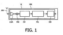
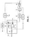
- Fig.1 describes an example of receiver device R in which the invention may be applied. It is important to notice that the invention is not limited to receiver devices. Indeed it applies also to transceiver device, and more generally to any type of device adapted to receive analog radio signals to be converted into digital signals.
- the receiver (or transceiver) device R is intended for mobile communication equipment such as a mobile phone, for instance a GSM or GPRS/EDGE or UMTS mobile phone, or Bluetooth or WLAN (Wireless Local Area Network) communication equipment.
- mobile communication equipment such as a mobile phone, for instance a GSM or GPRS/EDGE or UMTS mobile phone, or Bluetooth or WLAN (Wireless Local Area Network) communication equipment.
- the invention is not limited to this type of radio communication equipment.
- it may also be used for television on mobile applications (DVB-H), and for all DVB standards (DVB-S, DVB-T or DVB-C, for instance).
- a receiver (device) R notably comprises an antenna AN adapted to receive analog modulated signals and a processing module PM fed with the received analog signals.
- the processing module PM comprises a low noise amplifier LNA arranged to amplify the analog signals received by the antenna AN to feed a mixer MX which feeds a continuous-time sigma-delta analog-to-digital converter or CT ⁇ ADC (hereafter named "converter”) CV according to the invention, arranged to convert and filter the amplified analog signals into digital signals to feed a module M1 dedicated to channel filtering and noise-shaping digital filtering and feeding a digital demodulator DD arranged to demodulate the filtered digital signals.
- LNA low noise amplifier
- CT ⁇ ADC continuously-time sigma-delta analog-to-digital converter
- the converter CV comprises at least a signal path SP comprising at least one combiner C1 for combining the amplified analog signals to be converted with feedback analog signals, at least two integrators H1 and H2, mounted in series, for integrating the combined analog signals output by the combiner C 1, a quantizer Q for converting the integrated signals output by the integrators H1 and H2 into digital signals Y, and a decimation filter DF for filtering the high-frequency quantization noise and reducing the bitstream data rate, and outputting filtered digital signals Y d .
- the converter CV comprises five integrators H1-H5 mounted in series in the signal path SP to define a 5-th order filter.
- the number of integrators (and then the order of the filter) is not limited to this example. It may be equal to any value greater than 2 to define at least a 2nd order filter in the signal path SP.
- OTA-RC Orthogonal Transconductance Amplifier-RC
- the converter CV further comprises a feedback path FP comprising at least a digital-to-analog converter DAC arranged to convert the digital signals Y output by the quantizer Q into feedback analog signals intended for the combiner C1 (at least).
- the feedback path FP could be provided with at least one analog weighting means arranged to apply a chosen weighting coefficient to the feedback analog signals output by the DAC to convert them into weighted feedback analog signals intended for the combiner C1.
- the analog weighting means may be transconductances or voltage attenuators, for instance. They are used to stabilize the ADC loop.
- the signal path SP must comprise one combiner before each integrator in order to feed the latter with combined received analog signals and weighted feedback analog signals. Each combiner is then arranged to subtract the weighted feedback analog signals it receives from the associated analog weighting means from the analog signals it receives either from the mixer MX or from the preceding integrator Hj-1.
- the converter CV may have a feedback and/or feedforward topology.
- FIG.2 A non mandatory 1-bit, single-loop, feedforward topology is illustrated in Fig.2 . More precisely in this example of embodiment the converter CV comprises two local resonator feedback means b1 and b2 mounted in parallel with the signal path SP. These local resonator feedback means may be transconductances or voltage attenuators, for instance. They are used to create notch(es) in the noise transfer function (NTF) to optimize the signal-to-quantization noise ratio (SQNR) in the bandwidth.
- NTF noise transfer function
- SQL signal-to-quantization noise ratio
- Each local resonator feedback means b1 or b2 is arranged to weight the integrated analog signals output by a chosen integrator H3 or H5 with a chosen coefficient to feed a combiner C2 or C3 with weighted analog signals, which combiner is located in the signal path SP before the integrator H2 or H4, itself located before this chosen integrator H3 or H5.
- each combiner (here C2 and C3) has an additional additive input to combine the integrated analog signals output by the preceding integrator (H1 or H3) with the weighted analog signals output by the local resonator feedback means b1 or b2 (and possibly with weighted feedback analog signals output by analog weighting means).
- the converter CV may comprise only one local resonator feedback means (for instance b1 or b2) or more than two local resonator feedback means when the number of integrators Hj (or the filter order) is greater than or equal to 4.
- the converter CV further comprises four weighted feedforward summation path a1-a4 mounted in parallel with the signal path SP, respectively between the output of the first H1, second H2, third H3 and fourth H4 integrators and the fourth combiner C4, and another weighted feedforward summation means a5 mounted in series in the signal path SP between the output of the fifth integrator H5 and the fourth combiner C4.
- Each weighted feedforward summation path or means aj is arranged to weight, with a chosen coefficient, the integrated analog signals output by the preceding integrator (here Hj) to feed the fourth combiner C4 with weighted analog signals.
- the fourth combiner C4 has as many additive inputs as weighted feedforward summation paths and means aj (here five) to feed the quantizer Q with the sum of all the weighted integrated analog signals output by the integrators H1-H5.
- weighted feedforward summation paths and means aj are also used to stabilize the ADC loop. Therefore, they may be mixed with the analog weighting means dj to maximize the advantages and minimize the drawbacks of the two topologies. But the cumulated number of weighted feedforward summation paths and means aj and analog weighting means must be equal to the filter order (L).
- the invention proposes to integrate digital self-calibration means into the converter CV to allow calibration of the analog capacitors and/or resistors of at least one RC integrator Hj, to compensate process variations and temperature spread.
- At least one integrator Hj of the converter CV comprises variable capacitance means Cj and/or variable resistance means Rj.
- the integrators H1 and H5 (but this is also the case of integrators H2 to H4 of Fig.2 ) only comprise a variable capacitance means Cj arranged to be set in chosen states depending on the values of a digital word. So a specific capacitance value of each variable capacitor means Cj of each integrator Hj corresponds to each digital word value.
- the feedforward coefficients Aj are implemented with resistors, but they could be also implemented with capacitors.
- each integrator Hj comprises a transconductance Tj with a differential input and a differential output.
- Each differential input receives differential analog signals coming either from differential input nodes N1 and N2 of the converter CV (case of H1) or from a differential output of the preceding integrator Hj-1 (case of H2 to H5), through a resistor Rj (which can be variable and addressable by the digital word).
- a two-state control switch SW may be provided between the first N1 and second N2 differential input nodes.
- each integrator Hj comprises a transconductance Tj with a single-ended input fed with analog signals and a single-ended output.
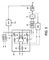
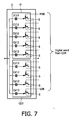
- variable capacitance means Cj A non-limiting example of embodiment of a variable capacitance means Cj is illustrated in Fig.7 .
- the variable capacitance means Cj consists of 9 couples connected in parallel and each comprising a capacitor, with a chosen capacitance, and a two-state switch S mounted in series with the capacitor.
- Each two-state switch S is controlled by one bit value of the digital word generated by a self-calibration control module CCM which will be described below.
- the number of couples may be equal to 9.
- the nine capacitors mounted in parallel offer together a maximum capacitance value equal to 4/3 of a starting capacitance Ci (4Ci/3).
- a first one of the nine capacitors has a value equal to 2/3 of the starting capacitance Ci (2Ci/3), while each one of the eight other capacitors has a value equal to 1/12 of the starting capacitance Ci (Ci/12), for instance.
- the switch S connected to the first capacitor is preferably controlled by the digital word bit having the most significant weight (MSB), while the switch S connected to the last (or ninth) capacitor (with a capacitance value equal to Ci/12) is controlled by the digital word bit being the least significant bit (LSB).
- first and second parts into a variable capacitance means Cj.
- the first part comprises the first to fifth couples and offers a maximum capacitance value equal to the starting capacitance Ci
- the second part comprises the sixth to ninth couples and offers a maximum capacitance value equal to 1/3 of the starting capacitance Ci (Ci/3).
- this arrangement allows to vary the capacitance value of each variable capacitance means Cj by a decrement (or increment) equal to 1/12 of the starting capacitance Ci (Ci/12).
- variable resistance means Rj A non-limiting example of embodiment of a variable resistance means Rj (with j ⁇ 1 as will be explained below) is illustrated in Fig.8 .
- the variable resistance means Rj consists of nine resistors, connected in series and having chosen respective resistances, and nine two-state switches connected in parallel between the last resistor and two consecutive resistors, respectively.
- Each two-state switch S is controlled by one bit value of the digital word generated by the self-calibration control module CCM.
- the number of couples may be equal to 9.
- the nine resistors mounted in series offer together a maximum resistance value equal to 4/3 of a starting resistance Ri (4Ri/3).
- a first one of the nine resistors has a value equal to 2/3 of the starting resistance Ri (2Ri/3), while each one of the eight other resistors has a value equal to 1/12 of the starting resistance Ri(Ri/12), for instance.
- the switch S connected to the first resistor on the right side (to offer a cumulative resistance value equal to 4Ri/3) is preferably controlled by the digital word bit being the most significant bit (MSB), while the switch S connected to the last (or ninth) resistor on the left (to offer a resistance value equal to 2Ri/3) is controlled by the digital word bit being the least significant bit (LSB).
- MSB most significant bit
- LSB least significant bit
- first and second parts into a variable resistance means Rj.
- the first part comprises the first to fifth resistors and offers a maximum resistance value equal to the starting resistance Ri
- the second part comprises the sixth to ninth resistors and offers a maximum resistance value equal to 1/3 of the starting resistance Ri (Ri/3).
- each variable resistance means Rj (with j ⁇ 1) by a decrement (or increment) equal to 1/12 of the starting resistance Ri (Ri/12).
- the digital-to-analog converter DAC of the feedback path FP has one input connected to the signal path SP to be fed with digital signals Y and differential outputs connected to the differential inputs of the first integrator H1.
- a DAC may be a switched capacitor DAC, for instance.
- the digital-to-analog converter DAC of the feedback path FP has one input connected to the signal path SP to be fed with digital signals Y and one output connected to the single-ended input of the first integrator H1.
- each integrator Hj comprises two banks of variable capacitors Cj respectively connected in series with resistances rj (not variable - each resistance "rj" helps to stabilize the OTA-RC structure and has preferably a different value for each integrator Hj) into a differential feedback path.
- each integrator Hj comprises one bank of variable capacitors Cj respectively connected in series with resistances rj in a single-ended feedback path.
- the optional weighted feedforward summation paths and means a1-a5 are differential.
- the optional local resonator feedback means b1 and b2 are differential.
- the converter CV according to the invention also comprises a self-calibration control module CCM having an input connected to the signal path SP after the decimation filter DF, to be fed with filtered digital signals Y d , and coupled to each variable capacitor means Cj and/or each variable resistor means Rj, to provide it (them) with a chosen digital word to control its (their) capacitance and/or resistance.
- CCM self-calibration control module having an input connected to the signal path SP after the decimation filter DF, to be fed with filtered digital signals Y d , and coupled to each variable capacitor means Cj and/or each variable resistor means Rj, to provide it (them) with a chosen digital word to control its (their) capacitance and/or resistance.
- This self-calibration control module CCM is arranged to implement a calibration algorithm comprising the following four main steps.
- a) the self-calibration control module CCM generates a digital word with a chosen first value. This value corresponds to a chosen first capacitance value and/or first resistance value of each variable capacitor means Cj and/or each variable resistor means Rj (with j ⁇ 1, i.e. R2 to R5).
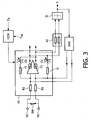
- the converter CV comprises integrators Hj such as the one illustrated in Fig.3
- the first value of the digital word corresponds to a first capacitance of each variable capacitor means Cj equal to a chosen starting capacitance Ci with a chosen increase step.
- This starting capacitance Ci corresponds preferably to a chosen spread of the integrator RC product (or time constant).
- the nominal value for a component Ropt and Copt for instance
- the standard deviation from this nominal value due to process variations and temperature spread are well known inputs and are included in the modeling of the components. These inputs are used to set the starting capacitance Ci.
- Copt Copt.
- the capacitance step must not only compensate for the capacitance variations but also for the resistance variations and temperature spread.
- the process variations and temperature spread depend on the technology (for instance they are different in CMOS 90 nm and CMOS 65 nm). Therefore, the Ci value must be chosen according to the CMOS technology used for the design.
- the chosen increase step of the starting capacitance Ci may be equal to 33% (1/3) of this starting capacitance Ci, for instance +Ci/3. So, in this case the first value of the digital word corresponds to a first capacitance of each variable capacitance means Cj equal to 4Ci/3 (Ci + Ci/3).
- This example of chosen increase step (+33%) is well adapted to the examples of variable capacitance means Cj and variable resistance means Rj described above with reference to Figs.7 and 8 .
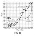
- These examples of embodiment of variable capacitance means Cj and variable resistance means Rj illustrated in Figs.7 and 8 allow a capacitance coverage corresponding to a RC spread comprised in the range [-25%; +33%].
- the IBN variations due to RC spread are not monotonic.
- the minimum of the IBN corresponds to the nominal RC value (no spread).
- the absolute value of the IBN depends on the circuit noise. Since the circuit noise is temperature dependent, the absolute value of the IBN will vary depending on the die temperature during the calibration process. So, it is desirable to calibrate the RC product with a constant circuit noise.
- resistor(s) R1 of the first integrator H1 is(are) usually the main noise contributor(s). So, it is not desirable to increase the resistance value of resistor(s) R1 and thus their thermal noise contribution because this would increase the total in-band noise (IBN) and reduce the signal-to-noise ratio (SNR). This situation happens as soon as the unity-gain frequencies of the integrators Hj are too high (i.e. when the RC product is smaller than the nominal one).
- the loop filter topology being not sensitive to unity-gain variations of the first integrator H1, but very sensitive to the unity-gain frequency of the second to fifth integrators H2 to H5, a resistance calibration of the resistors Rj of each integrator Hj, except the first one H1, can be carried out. It is also possible to calibrate the capacitance value of the capacitors Cj of each integrator Hj and the resistance of the resistors Rj of each integrator Hj, except the first one H1.
- the self-calibration control module CCM may comprise an estimation module such as the one illustrated as an example in Fig.9 .
- the upper branch (sub-modules SM1-SM4) determines the first member of the right part of the relation (P Q ) cited above
- the lower branch (sub-modules SMS-SM8) determines the second member of the right part of the relation cited above
- the combiner SM9 subtracts the value provided by the sub-modules SM5-SM8 of the second branch from the value provided by the sub-modules SM1-SM4 of the first branch.
- the self-calibration control module CCM stores it in a register A and compares it to the preceding estimated in-band noise IBN(n-1), stored in a register B.
- the self-calibration control module CCM modifies the value of the digital word generated last in order to decrease the current capacitance value Ci of each variable capacitance means Cj of each integrator Hj from a chosen decrement Cstep and/or the resistance value of each variable resistance means Rj of each integrator Hj except the first one H1, when IBN(n) is smaller than IBN(n-1).
- This decrement Cstep (or Rstep) may be equal to a chosen proportion of the starting capacitance Ci (or starting resistance Rj). It depends on the final accuracy.
- the decrement Cstep (or Rstep) may be equal to Ci/12 (or Ri/12) when a +/-10% accuracy on the RC spread must be achieved. It is worth noting that the IBN must be predicted with less accuracy, which fixes the number of samples N s required for the IBN estimation.
- This example of decrement is well adapted to the examples of variable capacitance means Cj and variable resistance means Rj described above with reference to Figs.7 and 8 .
- variable capacitance means Cj and variable resistance means Rj illustrated in Figs.7 and 8 allow to choose a decrement Cstep (or Rstep) situated in the range [Copt/15; Copt/10] (or [Ropt/15; Ropt/10]) when the accuracy is situated in the range [5%; 10%], for an initial capacitance (or resistance) increase step equal to 33%. So, the value of the decrement depends on the accuracy wanted.
- a fourth main step d) the self-calibration control module CCM iterates steps b) and c) till the currently estimated IBN(n) is equal to or greater than the previously estimated IBN(N-1). At most 9 iterations are necessary to converge to a final calibration value of the digital word.
- the self-calibration control module CCM chooses as the final calibration value of the digital word the value that corresponds to IBN(n-1). Then it generates this final calibration value in order to set the calibration state of each variable capacitance means Cj and/or each variable resistance means Rj.
- a preliminary starting step 10 one specifies in the self-calibration control module CCM the number N S of samples to be used for estimating the IBN, and the length of two registers A and B respectively intended for storing the current IBN estimate (IBN(n)) and the preceding IBN estimate (IBN(n-1)).
- the self-calibration control module CCM carries out a test to determine whether a calibration must be started or not.
- the calibration algorithm ends in a step 30 in which the self-calibration control module CCM may decide not to shortcut the differential input nodes N1 and N2 of the converter CV, for instance.
- the self-calibration control module CCM may start by shortcutting the differential input nodes N1 and N2 of the converter CV by means of the control switch SW illustrated in Fig.3 .
- This shortcutting operation is not mandatory because converter CV is self-biased due to the feedback mechanism. But this is preferable in order to avoid any distortion effect that could corrupt the IBN estimation.
- the self-calibration control module CCM stores the estimated IBN value (IBN(1)) in register A.
- the self-calibration control module CCM carries out a test to determine if the value of the counter is greater than 1 (Count > 1).
- the self-calibration control module CCM carries out another test in a step 90 to determine whether the value stored in register A is smaller than the value stored in register B.
- the self-calibration control module CCM carries out a step 110 in which it chooses the value that corresponds to IBN(n-1), stored in register B, as the final calibration value of the digital word. So it generates this final calibration value in order to set the calibration state of each variable capacitor means Cj. And the calibration algorithm ends in a final step 120.
- the converter CV is an integrated circuit IC, and possibly a baseband integrated circuit.
- Such an integrated circuit may be realized in CMOS technology or in any technology currently used in chip manufacture, and notably in AsGa or BiCMOS technology.
- a converter CV according to the invention offers several advantages, and notably:
- the invention is not limited to the embodiments of continuous-time sigma-delta analog-to-digital converter, (baseband) integrated circuit, receiver device, transceiver device and radio communication equipment described above only by way of example, but it includes all alternative embodiments which may be considered by one skilled in the art to be within the scope of the claims hereafter.
Claims (25)
- Zeitkontinuierlicher Sigma-Delta-Analog-zu-Digital-Wandler (CV) zum Wandeln analoger Signale in digitale Signale, umfassend: i) einen Signalweg (SP), der wenigstens einen Kombinator (C1), der so ausgeführt ist, dass er zu konvertierende analoge Signale mit analogen Rückkopplungssignalen kombiniert, wenigstens zwei Integratoren (Hj), die in Reihe montiert sind und so ausgeführt sind, dass sie die kombinierten analogen Signale integrieren, einen Quantisierer (Q), der so ausgeführt ist, dass er die integrierten Signale in digitale Signale wandelt, und ein Dezimationsfilter (DF) zum Filtern digitaler Signale umfasst; und ii) einen Rückkopplungsweg (FP), der wenigstens einen Digital-zu-Analog-Wandler (DAC) umfasst, der so ausgeführt ist, dass er die vom Quantisierer (Q) ausgegebenen digitalen Signale in analoge Rückkopplungssignale wandelt, die für den Kombinator (C1) vorgesehen sind, wobei wenigstens einer der Integratoren (Hj) veränderliche Kapazitätsmittel (Cj) und/oder veränderliche Widerstandsmittel (Rj) umfasst, die so ausgeführt sind, dass sie in Abhängigkeit von den Werten eines digitalen Wortes in ausgewählte Zustände versetzt werden, um ausgewählte Kapazitätswerte und/oder ausgewählte Widerstandswerte darzustellen, und ferner ein Selbstkalibrierungs-Steuermittel (CCM) umfasst, dadurch gekennzeichnet, dass das Selbstkalibrierungs-Steuermittel (CCM) so ausgeführt ist, dass es a) ein digitales Wort mit einem ausgewählten ersten Wert erzeugt, b) anschließend das bandinterne Rauschen IBN(n) anhand der gefilterten digitalen Signale schätzt und das bandinterne Rauschen IBN(n) mit dem vorangehenden bandinternen Rauschen IBN(n-1) vergleicht, c) anschließend den Wert des digitalen Wortes modifiziert, um den Kapazitätswert und/oder den Widerstandswert jedes betreffenden Integrators (Hj) ausgehend von einem ausgewähltem Dekrement zu verringern, wenn IBN(n) kleiner ist als IBN(n-1), d) anschließend die Schritte b) und c) wiederholt, bis IBN(n) gleich oder größer als IBN(n-1) ist, und als digitalen Kalibrierungswortwert den Wert auswählt, der dem vorangehenden bandinternen Rauschen IBN(n-1) entspricht, um den Kalibrierungszustand festzulegen.
- Wandler nach Anspruch 1, dadurch gekennzeichnet, dass jedes veränderliche Kapazitätsmittel (Cj) eine ausgewählte Anzahl von Bänken von Kapazitäten mit einem ausgewählten Kapazitätswert umfasst, die in Reihe mit einem Zwei-Zustand-Schalter (s) montiert sind, der durch einen Bitwert des digitalen Wertes gesteuert wird.
- Wandler nach Anspruch 2, dadurch gekennzeichnet, dass im Schritt a) das Selbstkalibrierungs-Steuermittel (CCM) so ausgeführt ist, dass es ein digitales Wort erzeugt, das einen ersten Wert aufweist, der einem ersten Kapazitätswert gleich einem gewählten Anfangskapazitätswert (Ci) mit einem ausgewählten Erhöhungsschritt entspricht.
- Wandler nach Anspruch 3, dadurch gekennzeichnet, dass der Anfangskapazitätswert (Ci) einer gegebenen Streuung des Integrator-RC-Produkts entspricht.
- Wandler nach irgendeinem der Ansprüche 3 und 4, dadurch gekennzeichnet, dass der ausgewählte Erhöhungsschritt gleich 33% des Anfangskapazitätswertes (Ci) ist.
- Wandler nach irgendeinem der Ansprüche 3 bis 5, dadurch gekennzeichnet, dass das Dekrement (Cstep) gleich einem ausgewähltem Anteil des Anfangskapazitätswertes (Ci) abhängig von einem Prozessvariationswert, einer Temperaturstreuung und einer endgültigen Sollgenauigkeit ist.
- Wandler nach irgendeinem der Ansprüche 5 und 6, dadurch gekennzeichnet, dass die Anzahl der Kapazitäten gleich neun ist, wobei die neun Kapazitäten gemeinsam einen maximalen Wert gleich 4/3 des Anfangskapazitätswertes (Ci) bieten, eine erste der neun Kapazitäten einen Wert gleich 2/3 des Anfangskapazitätswertes (Ci) aufweist, jede der acht anderen Kapazitäten einen Wert gleich 1/12 des Anfangskapazitätswertes (Ci) aufweist, und das Dekrement gleich 1/12 des Anfangskapazitätswertes (Ci) ist.
- Wandler nach irgendeinem der Ansprüche 1 bis 7, dadurch gekennzeichnet, dass jedes veränderliche Widerstandsmittel (Rj) eine ausgewählte Anzahl von Widerständen umfasst, die in Reihe verbunden sind und ausgewählte entsprechende Widerstandswerte und eine gleiche ausgewählte Anzahl von Zwei-Zustand-Schaltern (s) aufweisen, die jeweils durch einen Bitwert des digitalen Wortes gesteuert werden und entsprechend die Zugriffe auf die Widerstände steuern.
- Wandler nach Anspruch 8, dadurch gekennzeichnet, dass im Schritt a) das Selbstkalibrierungs-Steuermittel (CCM) so ausgeführt ist, dass es ein digitales Wort erzeugt, das einen ersten Wert aufweist, der einem ersten Widerstandswert gleich einem gewählten Anfangswiderstandswert (Ri) mit einem ausgewähltem Erhöhungsschritt entspricht.
- Wandler nach Anspruch 9, dadurch gekennzeichnet, dass der Anfangswiderstandswert (Ri) einer ausgewählten Streuung des Integrator-RC-Produkts entspricht.
- Wandler nach irgendeinem der Ansprüche 9 und 10, dadurch gekennzeichnet, dass der ausgewählte Erhöhungsschritt gleich 33% des Anfangswiderstandswertes ist.
- Wandler nach irgendeinem der Ansprüche 9 bis 11, dadurch gekennzeichnet, dass das Dekrement (Rstep) gleich einem ausgewähltem Anteil des Anfangswiderstandswertes (Ri) ist.
- Wandler nach irgendeinem der Ansprüche 11 und 12, dadurch gekennzeichnet, dass die Anzahl der Widerstände gleich neun ist, wobei die neun Widerstände gemeinsam einen maximalen Wert gleich 4/3 des Anfangswiderstandswertes (Ri) bieten, ein erster der neun Widerstände einen Wert gleich 2/3 des Anfangswiderstandwertes (Ri) aufweist, jeder der acht anderen Widerstände einen Wert gleich 1/12 des Anfangswiderstandswertes (Ri) aufweist, und das Dekrement (Rstep) gleich 1/12 der Anfangswiderstandswertes (Ri) ist.
- Wandler nach irgendeinem der Ansprüche 1 bis 13, dadurch gekennzeichnet, dass er so ausgeführt ist, dass er in einem Differenzialmodus arbeitet und zwei Differenzialeingangsknoten (N1, N2) umfasst, die so ausgeführt sind, dass sie mit differenziellen Analogsignalen gespeist werden, die zu wandeln sind.
- Wandler nach Anspruch 14, dadurch gekennzeichnet, dass die zwei differenziellen Eingangsknoten (N1, N2) während der Kalibrierungsschritte a) bis d) kurzgeschlossen sind.
- Wandler nach irgendeinem der Ansprüche 1 bis 15, dadurch gekennzeichnet, dass der Signalweg (SP) fünf unterschiedliche Integratoren (H1-H5) umfasst, die in Reihe montiert sind.
- Wandler nach irgendeinem der Ansprüche 1 bis 16, dadurch gekennzeichnet, dass der Digital-zu-Analog-Wandler (DAC) und der Quantisierer (Q) dem Einzel-Bit-Typ oder dem Multi-Bit-Typ entsprechen.
- Wandler nach irgendeinem der Ansprüche 1 bis 17, dadurch gekennzeichnet, dass er mit einer Filterschleife aufgebaut ist.
- Wandler nach irgendeinem der Ansprüche 1 bis 17, dadurch gekennzeichnet, dass er aufgebaut ist, indem mehrere CT-ΣΔ-ADC-Stufen kaskadiert sind, die jeweils entweder ein CT-ΣΔ-ADC erster Ordnung oder ein CT-ΣΔ-ADC oder ein zweiter Ordnung sind.
- Wandler nach irgendeinem der Ansprüche 1 bis 19, dadurch gekennzeichnet, dass er Hochfrequenz-Stabilisierungsmittel umfasst.
- Integrierte Schaltung, dadurch gekennzeichnet, dass sie einen Wandler (CV) nach irgendeinem der vorangehenden Ansprüche umfasst.
- Integrierte Schaltung nach Anspruch 21, dadurch gekennzeichnet, dass sie eine integrierte Basisband-Schaltung definiert.
- Empfangsvorrichtung, dadurch gekennzeichnet, dass sie eine integrierte Schaltung nach irgendeinem der Ansprüche 21 und 22 umfasst.
- Sendevorrichtung, dadurch gekennzeichnet, dass sie einen Wandler (CV) nach irgendeinem der Ansprüche 1 bis 20 umfasst.
- Mobilfunk-Kommunikationseinrichtung, dadurch gekennzeichnet, dass sie einen Wandler (CV) oder eine integrierte Schaltung oder eine Empfangsvorrichtung oder eine Sendevorrichtung nach irgendeinem der vorangehenden Ansprüche umfasst.
Priority Applications (1)
| Application Number | Priority Date | Filing Date | Title |
|---|---|---|---|
| EP07700660A EP1980021B1 (de) | 2006-01-25 | 2007-01-22 | Zeitkontinuierlicher sigma-delta-analog-digital-wandler mit selbstkalibrierung für kondensator und/oder widerstand für rc-spreizungskompensation |
Applications Claiming Priority (3)
| Application Number | Priority Date | Filing Date | Title |
|---|---|---|---|
| EP06300070 | 2006-01-25 | ||
| PCT/IB2007/050213 WO2007085997A1 (en) | 2006-01-25 | 2007-01-22 | Continuous-time sigma-delta analog-to-digital converter with capacitor and/or resistance digital self-calibration means for rc spread compensation |
| EP07700660A EP1980021B1 (de) | 2006-01-25 | 2007-01-22 | Zeitkontinuierlicher sigma-delta-analog-digital-wandler mit selbstkalibrierung für kondensator und/oder widerstand für rc-spreizungskompensation |
Publications (2)
| Publication Number | Publication Date |
|---|---|
| EP1980021A1 EP1980021A1 (de) | 2008-10-15 |
| EP1980021B1 true EP1980021B1 (de) | 2009-12-02 |
Family
ID=37951898
Family Applications (1)
| Application Number | Title | Priority Date | Filing Date |
|---|---|---|---|
| EP07700660A Active EP1980021B1 (de) | 2006-01-25 | 2007-01-22 | Zeitkontinuierlicher sigma-delta-analog-digital-wandler mit selbstkalibrierung für kondensator und/oder widerstand für rc-spreizungskompensation |
Country Status (8)
| Country | Link |
|---|---|
| US (1) | US7944385B2 (de) |
| EP (1) | EP1980021B1 (de) |
| JP (1) | JP2009524966A (de) |
| KR (1) | KR20080097442A (de) |
| CN (1) | CN101375507B (de) |
| AT (1) | ATE450930T1 (de) |
| DE (1) | DE602007003564D1 (de) |
| WO (1) | WO2007085997A1 (de) |
Cited By (1)
| Publication number | Priority date | Publication date | Assignee | Title |
|---|---|---|---|---|
| DE102015110846B4 (de) * | 2014-07-17 | 2020-08-13 | Analog Devices Global | Analog-Digitalwandler und Verfahren zum Eichen desselben |
Families Citing this family (35)
| Publication number | Priority date | Publication date | Assignee | Title |
|---|---|---|---|---|
| US7960772B2 (en) | 2007-04-26 | 2011-06-14 | Peregrine Semiconductor Corporation | Tuning capacitance to enhance FET stack voltage withstand |
| US20090085785A1 (en) * | 2007-09-28 | 2009-04-02 | Friedel Gerfers | Digital-to-analog converter calibration for multi-bit analog-to-digital converters |
| EP2760136B1 (de) | 2008-02-28 | 2018-05-09 | Peregrine Semiconductor Corporation | Verfahren und Vorrichtung zur Verwendung beim digitalen Abstimmen eines Kondensators in einer integrierten Schaltungsvorrichtung |
| CN101299599B (zh) * | 2008-06-16 | 2011-12-28 | 华为技术有限公司 | 获取跨导滤波器校准电容值的方法、装置和系统 |
| KR101575245B1 (ko) * | 2009-02-17 | 2015-12-09 | 삼성전자주식회사 | Rc 시정수 보상기를 이용한 아날로그 디지털 변환방법 및이를 위한 아날로그 디지털 변환 장치 |
| US8299947B2 (en) * | 2009-06-26 | 2012-10-30 | Syntropy Systems, Llc | Sampling/quantization converters |
| US8634766B2 (en) * | 2010-02-16 | 2014-01-21 | Andrew Llc | Gain measurement and monitoring for wireless communication systems |
| US8018365B1 (en) * | 2010-03-14 | 2011-09-13 | Mediatek Inc. | Continuous-time delta-sigma ADC with compact structure |
| US8711980B2 (en) | 2010-09-10 | 2014-04-29 | Intel IP Corporation | Receiver with feedback continuous-time delta-sigma modulator with current-mode input |
| WO2012073117A1 (en) * | 2010-12-03 | 2012-06-07 | Marvell World Trade Ltd. | A continuous time sigma-delta adc with embedded low-pass filter |
| US8643518B2 (en) * | 2010-12-30 | 2014-02-04 | Mediatek Singapore Pte. Ltd. | Calibration of time constants in a continuous-time delta-sigma converter |
| TWI452847B (zh) | 2011-01-21 | 2014-09-11 | Mediatek Singapore Pte Ltd | 類比至數位轉換器 |
| US8552894B2 (en) * | 2011-06-15 | 2013-10-08 | Mediatek Inc. | Sigma-delta modulator having a feed-forward path and a hybrid portion |
| CN102832945B (zh) * | 2011-06-15 | 2015-03-04 | 联发科技股份有限公司 | Σ-δ调制器 |
| US8519873B2 (en) * | 2011-09-09 | 2013-08-27 | Texas Instruments Incorporated | Correcting for non-linearities in a continuous-time sigma-delta modulator |
| US8791848B2 (en) * | 2012-02-22 | 2014-07-29 | Mediatek Inc. | Sigma-delta modulators with excess loop delay compensation |
| US8947142B2 (en) | 2012-05-16 | 2015-02-03 | Cypress Semiconductor Corporation | Common mode trimming with variable duty cycle |
| US20130314271A1 (en) * | 2012-05-25 | 2013-11-28 | Brandt Braswell | Vehicle-borne radar systems with continuous-time, sigma delta analog-to-digital converters, and methods of their operation |
| ITMI20121116A1 (it) * | 2012-06-26 | 2013-12-27 | St Microelectronics Srl | Anello di conversione analogico-digitale particolarmente per sistemi psi5 e wss |
| KR20140001565A (ko) | 2012-06-27 | 2014-01-07 | 한국전자통신연구원 | 시정수 보정 장치 및 방법과 이를 포함한 저역 통과 델타 시그마 변조 장치 |
| TWI493884B (zh) * | 2012-08-28 | 2015-07-21 | Univ Nat Chiao Tung | 三角積分調變器及其校正方法 |
| US9543978B2 (en) | 2013-02-21 | 2017-01-10 | Telefonaktiebolaget Lm Ericsson (Publ) | Frequency selective circuit configured to convert an analog input signal to a digital output signal |
| DE102013007030A1 (de) * | 2013-04-24 | 2014-10-30 | Micronas Gmbh | Zeitkontinuierlicher Delta-Sigma-Modulator |
| US9407238B2 (en) | 2014-08-28 | 2016-08-02 | Qualcomm Technologies International, Ltd. | Devices and methods for pulse-width modulation |
| JP6910301B2 (ja) * | 2015-02-20 | 2021-07-28 | コミサリヤ・ア・レネルジ・アトミク・エ・オ・エネルジ・アルテルナテイブ | 高直線性シグマ−デルタ変換器 |
| CN107810604B (zh) * | 2015-04-01 | 2021-04-16 | Tdk株式会社 | 西格玛-德尔塔调制器装置、用于校准连续时间西格玛-德尔塔调制器的方法以及控制装置 |
| US9379728B1 (en) * | 2015-06-26 | 2016-06-28 | Stmicroelectronics International N.V. | Self-calibrated digital-to-analog converter |
| US9438266B1 (en) * | 2016-02-10 | 2016-09-06 | Texas Instruments Incorporated | Calibrated-output analog-to-digital converter apparatus and methods |
| US9871504B2 (en) * | 2016-02-16 | 2018-01-16 | Analog Devices, Inc. | Differential phase adjustment of clock input signals |
| CN108123719A (zh) * | 2017-11-23 | 2018-06-05 | 天津工业大学 | 一种基于FPGA的Sigma-Delta调制器 |
| CN108415244B (zh) * | 2017-12-28 | 2020-12-18 | 中国空间技术研究院 | 一种多自由度静电悬浮系统几何对称性逼近方法 |
| CN111010188B (zh) * | 2019-12-03 | 2023-06-30 | 芯创智创新设计服务中心(宁波)有限公司 | 一种连续时间sigma-delta模数转换器的电阻电容校准电路 |
| US10862505B1 (en) | 2020-02-27 | 2020-12-08 | Nxp Usa, Inc. | Arbitrary rate decimator and timing error corrector for an FSK receiver |
| CN113452369B (zh) * | 2021-05-17 | 2022-09-20 | 清华大学深圳国际研究生院 | 一种模数转换器及其数字校准方法 |
| US11863205B2 (en) * | 2021-11-30 | 2024-01-02 | Analog Devices International Unlimited Company | Adaptive bias techniques for amplifiers in sigma delta modulators |
Family Cites Families (12)
| Publication number | Priority date | Publication date | Assignee | Title |
|---|---|---|---|---|
| US5625316A (en) * | 1994-07-01 | 1997-04-29 | Motorola, Inc. | Tuning circuit for an RC filter |
| US5574678A (en) * | 1995-03-01 | 1996-11-12 | Lattice Semiconductor Corp. | Continuous time programmable analog block architecture |
| US6069505A (en) * | 1997-03-20 | 2000-05-30 | Plato Labs, Inc. | Digitally controlled tuner circuit |
| US5914633A (en) * | 1997-08-08 | 1999-06-22 | Lucent Technologies Inc. | Method and apparatus for tuning a continuous time filter |
| IT1313303B1 (it) | 1999-07-06 | 2002-07-17 | Telital S P A Ora Telit Mobile | Apparecchio ricevente digitale multi-standard e metodo di definizionedi parametri in esso. |
| US6424209B1 (en) * | 2000-02-18 | 2002-07-23 | Lattice Semiconductor Corporation | Integrated programmable continuous time filter with programmable capacitor arrays |
| US6577258B2 (en) * | 2001-10-01 | 2003-06-10 | Nokia Corporation | Adaptive sigma-delta data converter for mobile terminals |
| US6639534B2 (en) * | 2002-02-14 | 2003-10-28 | Silicon Laboratories, Inc. | Digital-to-analog converter switching circuitry |
| US6954159B1 (en) * | 2003-07-01 | 2005-10-11 | Impinj, Inc. | Low distortion band-pass analog to digital converter with feed forward |
| US7034730B2 (en) * | 2003-10-03 | 2006-04-25 | Wright State University | Pipelined delta sigma modulator analog to digital converter |
| US6940436B2 (en) * | 2003-10-31 | 2005-09-06 | Texas Instruments Incorporated | Analog-to-digital conversion system with second order noise shaping and a single amplifier |
| US7095345B2 (en) * | 2004-06-29 | 2006-08-22 | Analog Devices, Inc. | Hybrid tuning circuit for continuous-time sigma-delta analog-to-digital converter |
-
2007
- 2007-01-22 US US12/161,532 patent/US7944385B2/en active Active
- 2007-01-22 EP EP07700660A patent/EP1980021B1/de active Active
- 2007-01-22 WO PCT/IB2007/050213 patent/WO2007085997A1/en active Application Filing
- 2007-01-22 CN CN2007800033060A patent/CN101375507B/zh active Active
- 2007-01-22 AT AT07700660T patent/ATE450930T1/de not_active IP Right Cessation
- 2007-01-22 KR KR1020087020753A patent/KR20080097442A/ko not_active Application Discontinuation
- 2007-01-22 DE DE602007003564T patent/DE602007003564D1/de active Active
- 2007-01-22 JP JP2008551923A patent/JP2009524966A/ja not_active Withdrawn
Cited By (1)
| Publication number | Priority date | Publication date | Assignee | Title |
|---|---|---|---|---|
| DE102015110846B4 (de) * | 2014-07-17 | 2020-08-13 | Analog Devices Global | Analog-Digitalwandler und Verfahren zum Eichen desselben |
Also Published As
| Publication number | Publication date |
|---|---|
| DE602007003564D1 (de) | 2010-01-14 |
| CN101375507A (zh) | 2009-02-25 |
| CN101375507B (zh) | 2011-04-13 |
| WO2007085997A1 (en) | 2007-08-02 |
| US7944385B2 (en) | 2011-05-17 |
| EP1980021A1 (de) | 2008-10-15 |
| ATE450930T1 (de) | 2009-12-15 |
| US20100219997A1 (en) | 2010-09-02 |
| JP2009524966A (ja) | 2009-07-02 |
| KR20080097442A (ko) | 2008-11-05 |
Similar Documents
| Publication | Publication Date | Title |
|---|---|---|
| EP1980021B1 (de) | Zeitkontinuierlicher sigma-delta-analog-digital-wandler mit selbstkalibrierung für kondensator und/oder widerstand für rc-spreizungskompensation | |
| US9735797B2 (en) | Digital measurement of DAC timing mismatch error | |
| US9543978B2 (en) | Frequency selective circuit configured to convert an analog input signal to a digital output signal | |
| Loeda et al. | A 10/20/30/40 MHz Feedforward FIR DAC Continuous-Time $\Delta\Sigma $ ADC With Robust Blocker Performance for Radio Receivers | |
| EP2119005B1 (de) | Vorrichtung mit einer frequenzselektiven schaltung und verfahren | |
| Breems et al. | A cascaded continuous-time/spl Sigma//spl Delta/Modulator with 67-dB dynamic range in 10-MHz bandwidth | |
| Breems et al. | A 56 mW Continuous-Time Quadrature Cascaded $\Sigma\Delta $ Modulator With 77 dB DR in a Near Zero-IF 20 MHz Band | |
| US8159380B2 (en) | Continuous-time sigma-delta analog-to-digital converter with non-invasive filter(s) for immunity preservation against interferers | |
| EP1604458B1 (de) | Mischtechnologie mems/bicmos lc bandpass-sigma-delta für direkte funkfrequenzabtastung | |
| US9178530B2 (en) | Delta sigma modulator, as well as receiver device and wireless communication device provided with same | |
| EP2229734B1 (de) | Multi-bit-sigma-delta-modulator mit reduzierter bitzahl im rückkopplungpfad | |
| US8223051B2 (en) | Multi-bit sigma-delta modulator with reduced number of bits in feedback path | |
| KR102317594B1 (ko) | 시그마-델타 변조기 | |
| US9648562B2 (en) | Transceiver front-end circuit for a cellular radio that employs components for reducing power consumption | |
| US7034730B2 (en) | Pipelined delta sigma modulator analog to digital converter | |
| CN108336998B (zh) | 模数转换装置与模数转换方法 | |
| Morgado et al. | Nanometer CMOS sigma-delta modulators for software defined radio | |
| US7495595B2 (en) | Analog-to-digital converter, receiver arrangement, filter arrangement and signal processing method | |
| Yamamoto et al. | A 63 mA 112/94 dB DR IF Bandpass $\Delta\Sigma $ Modulator With Direct Feed-Forward Compensation and Double Sampling | |
| Breems et al. | Continuous-time sigma-delta modulators for highly digitised receivers | |
| CN115694511A (zh) | 连续时间Sigma-Delta模数转换系统及其运行方法和应用 | |
| Bilhan | Very low power sigma delta modulator for WCDMA | |
| Gao | A survey on continuous-time modulators: theory, designs and implementations |
Legal Events
| Date | Code | Title | Description |
|---|---|---|---|
| PUAI | Public reference made under article 153(3) epc to a published international application that has entered the european phase |
Free format text: ORIGINAL CODE: 0009012 |
|
| 17P | Request for examination filed |
Effective date: 20080825 |
|
| AK | Designated contracting states |
Kind code of ref document: A1 Designated state(s): AT BE BG CH CY CZ DE DK EE ES FI FR GB GR HU IE IS IT LI LT LU LV MC NL PL PT RO SE SI SK TR |
|
| GRAP | Despatch of communication of intention to grant a patent |
Free format text: ORIGINAL CODE: EPIDOSNIGR1 |
|
| GRAS | Grant fee paid |
Free format text: ORIGINAL CODE: EPIDOSNIGR3 |
|
| GRAA | (expected) grant |
Free format text: ORIGINAL CODE: 0009210 |
|
| AK | Designated contracting states |
Kind code of ref document: B1 Designated state(s): AT BE BG CH CY CZ DE DK EE ES FI FR GB GR HU IE IS IT LI LT LU LV MC NL PL PT RO SE SI SK TR |
|
| REG | Reference to a national code |
Ref country code: GB Ref legal event code: FG4D |
|
| REG | Reference to a national code |
Ref country code: CH Ref legal event code: EP |
|
| REG | Reference to a national code |
Ref country code: IE Ref legal event code: FG4D |
|
| REF | Corresponds to: |
Ref document number: 602007003564 Country of ref document: DE Date of ref document: 20100114 Kind code of ref document: P |
|
| REG | Reference to a national code |
Ref country code: NL Ref legal event code: VDEP Effective date: 20091202 |
|
| PG25 | Lapsed in a contracting state [announced via postgrant information from national office to epo] |
Ref country code: LT Free format text: LAPSE BECAUSE OF FAILURE TO SUBMIT A TRANSLATION OF THE DESCRIPTION OR TO PAY THE FEE WITHIN THE PRESCRIBED TIME-LIMIT Effective date: 20091202 Ref country code: FI Free format text: LAPSE BECAUSE OF FAILURE TO SUBMIT A TRANSLATION OF THE DESCRIPTION OR TO PAY THE FEE WITHIN THE PRESCRIBED TIME-LIMIT Effective date: 20091202 Ref country code: SE Free format text: LAPSE BECAUSE OF FAILURE TO SUBMIT A TRANSLATION OF THE DESCRIPTION OR TO PAY THE FEE WITHIN THE PRESCRIBED TIME-LIMIT Effective date: 20091202 |
|
| LTIE | Lt: invalidation of european patent or patent extension |
Effective date: 20091202 |
|
| PG25 | Lapsed in a contracting state [announced via postgrant information from national office to epo] |
Ref country code: CY Free format text: LAPSE BECAUSE OF FAILURE TO SUBMIT A TRANSLATION OF THE DESCRIPTION OR TO PAY THE FEE WITHIN THE PRESCRIBED TIME-LIMIT Effective date: 20091202 Ref country code: LV Free format text: LAPSE BECAUSE OF FAILURE TO SUBMIT A TRANSLATION OF THE DESCRIPTION OR TO PAY THE FEE WITHIN THE PRESCRIBED TIME-LIMIT Effective date: 20091202 Ref country code: SI Free format text: LAPSE BECAUSE OF FAILURE TO SUBMIT A TRANSLATION OF THE DESCRIPTION OR TO PAY THE FEE WITHIN THE PRESCRIBED TIME-LIMIT Effective date: 20091202 Ref country code: PL Free format text: LAPSE BECAUSE OF FAILURE TO SUBMIT A TRANSLATION OF THE DESCRIPTION OR TO PAY THE FEE WITHIN THE PRESCRIBED TIME-LIMIT Effective date: 20091202 |
|
| PG25 | Lapsed in a contracting state [announced via postgrant information from national office to epo] |
Ref country code: AT Free format text: LAPSE BECAUSE OF FAILURE TO SUBMIT A TRANSLATION OF THE DESCRIPTION OR TO PAY THE FEE WITHIN THE PRESCRIBED TIME-LIMIT Effective date: 20091202 |
|
| PG25 | Lapsed in a contracting state [announced via postgrant information from national office to epo] |
Ref country code: NL Free format text: LAPSE BECAUSE OF FAILURE TO SUBMIT A TRANSLATION OF THE DESCRIPTION OR TO PAY THE FEE WITHIN THE PRESCRIBED TIME-LIMIT Effective date: 20091202 Ref country code: RO Free format text: LAPSE BECAUSE OF FAILURE TO SUBMIT A TRANSLATION OF THE DESCRIPTION OR TO PAY THE FEE WITHIN THE PRESCRIBED TIME-LIMIT Effective date: 20091202 Ref country code: ES Free format text: LAPSE BECAUSE OF FAILURE TO SUBMIT A TRANSLATION OF THE DESCRIPTION OR TO PAY THE FEE WITHIN THE PRESCRIBED TIME-LIMIT Effective date: 20100313 Ref country code: PT Free format text: LAPSE BECAUSE OF FAILURE TO SUBMIT A TRANSLATION OF THE DESCRIPTION OR TO PAY THE FEE WITHIN THE PRESCRIBED TIME-LIMIT Effective date: 20100402 Ref country code: IS Free format text: LAPSE BECAUSE OF FAILURE TO SUBMIT A TRANSLATION OF THE DESCRIPTION OR TO PAY THE FEE WITHIN THE PRESCRIBED TIME-LIMIT Effective date: 20100402 Ref country code: EE Free format text: LAPSE BECAUSE OF FAILURE TO SUBMIT A TRANSLATION OF THE DESCRIPTION OR TO PAY THE FEE WITHIN THE PRESCRIBED TIME-LIMIT Effective date: 20091202 Ref country code: BG Free format text: LAPSE BECAUSE OF FAILURE TO SUBMIT A TRANSLATION OF THE DESCRIPTION OR TO PAY THE FEE WITHIN THE PRESCRIBED TIME-LIMIT Effective date: 20100302 |
|
| PG25 | Lapsed in a contracting state [announced via postgrant information from national office to epo] |
Ref country code: SK Free format text: LAPSE BECAUSE OF FAILURE TO SUBMIT A TRANSLATION OF THE DESCRIPTION OR TO PAY THE FEE WITHIN THE PRESCRIBED TIME-LIMIT Effective date: 20091202 Ref country code: MC Free format text: LAPSE BECAUSE OF NON-PAYMENT OF DUE FEES Effective date: 20100131 Ref country code: CZ Free format text: LAPSE BECAUSE OF FAILURE TO SUBMIT A TRANSLATION OF THE DESCRIPTION OR TO PAY THE FEE WITHIN THE PRESCRIBED TIME-LIMIT Effective date: 20091202 Ref country code: BE Free format text: LAPSE BECAUSE OF FAILURE TO SUBMIT A TRANSLATION OF THE DESCRIPTION OR TO PAY THE FEE WITHIN THE PRESCRIBED TIME-LIMIT Effective date: 20091202 |
|
| PLBE | No opposition filed within time limit |
Free format text: ORIGINAL CODE: 0009261 |
|
| STAA | Information on the status of an ep patent application or granted ep patent |
Free format text: STATUS: NO OPPOSITION FILED WITHIN TIME LIMIT |
|
| PG25 | Lapsed in a contracting state [announced via postgrant information from national office to epo] |
Ref country code: GR Free format text: LAPSE BECAUSE OF FAILURE TO SUBMIT A TRANSLATION OF THE DESCRIPTION OR TO PAY THE FEE WITHIN THE PRESCRIBED TIME-LIMIT Effective date: 20100303 |
|
| 26N | No opposition filed |
Effective date: 20100903 |
|
| PG25 | Lapsed in a contracting state [announced via postgrant information from national office to epo] |
Ref country code: IE Free format text: LAPSE BECAUSE OF NON-PAYMENT OF DUE FEES Effective date: 20100122 Ref country code: DK Free format text: LAPSE BECAUSE OF FAILURE TO SUBMIT A TRANSLATION OF THE DESCRIPTION OR TO PAY THE FEE WITHIN THE PRESCRIBED TIME-LIMIT Effective date: 20091202 |
|
| PG25 | Lapsed in a contracting state [announced via postgrant information from national office to epo] |
Ref country code: IT Free format text: LAPSE BECAUSE OF FAILURE TO SUBMIT A TRANSLATION OF THE DESCRIPTION OR TO PAY THE FEE WITHIN THE PRESCRIBED TIME-LIMIT Effective date: 20091202 |
|
| REG | Reference to a national code |
Ref country code: CH Ref legal event code: PL |
|
| PG25 | Lapsed in a contracting state [announced via postgrant information from national office to epo] |
Ref country code: CH Free format text: LAPSE BECAUSE OF NON-PAYMENT OF DUE FEES Effective date: 20110131 Ref country code: LI Free format text: LAPSE BECAUSE OF NON-PAYMENT OF DUE FEES Effective date: 20110131 |
|
| PG25 | Lapsed in a contracting state [announced via postgrant information from national office to epo] |
Ref country code: HU Free format text: LAPSE BECAUSE OF FAILURE TO SUBMIT A TRANSLATION OF THE DESCRIPTION OR TO PAY THE FEE WITHIN THE PRESCRIBED TIME-LIMIT Effective date: 20100603 Ref country code: LU Free format text: LAPSE BECAUSE OF NON-PAYMENT OF DUE FEES Effective date: 20100122 |
|
| PG25 | Lapsed in a contracting state [announced via postgrant information from national office to epo] |
Ref country code: TR Free format text: LAPSE BECAUSE OF FAILURE TO SUBMIT A TRANSLATION OF THE DESCRIPTION OR TO PAY THE FEE WITHIN THE PRESCRIBED TIME-LIMIT Effective date: 20091202 |
|
| PGFP | Annual fee paid to national office [announced via postgrant information from national office to epo] |
Ref country code: GB Payment date: 20121224 Year of fee payment: 7 |
|
| GBPC | Gb: european patent ceased through non-payment of renewal fee |
Effective date: 20140122 |
|
| PG25 | Lapsed in a contracting state [announced via postgrant information from national office to epo] |
Ref country code: GB Free format text: LAPSE BECAUSE OF NON-PAYMENT OF DUE FEES Effective date: 20140122 |
|
| REG | Reference to a national code |
Ref country code: FR Ref legal event code: PLFP Year of fee payment: 10 |
|
| REG | Reference to a national code |
Ref country code: FR Ref legal event code: PLFP Year of fee payment: 11 |
|
| REG | Reference to a national code |
Ref country code: FR Ref legal event code: PLFP Year of fee payment: 12 |
|
| P01 | Opt-out of the competence of the unified patent court (upc) registered |
Effective date: 20230724 |
|
| PGFP | Annual fee paid to national office [announced via postgrant information from national office to epo] |
Ref country code: FR Payment date: 20231219 Year of fee payment: 18 |
|
| PGFP | Annual fee paid to national office [announced via postgrant information from national office to epo] |
Ref country code: DE Payment date: 20231219 Year of fee payment: 18 |