EP1970883A2 - Ansteuerung und Ansteuerungsverfahren für lichtemittierende Anzeigevorrichtungen - Google Patents
Ansteuerung und Ansteuerungsverfahren für lichtemittierende Anzeigevorrichtungen Download PDFInfo
- Publication number
- EP1970883A2 EP1970883A2 EP08002641A EP08002641A EP1970883A2 EP 1970883 A2 EP1970883 A2 EP 1970883A2 EP 08002641 A EP08002641 A EP 08002641A EP 08002641 A EP08002641 A EP 08002641A EP 1970883 A2 EP1970883 A2 EP 1970883A2
- Authority
- EP
- European Patent Office
- Prior art keywords
- drive transistor
- light emitting
- switch
- drive
- circuit
- Prior art date
- Legal status (The legal status is an assumption and is not a legal conclusion. Google has not performed a legal analysis and makes no representation as to the accuracy of the status listed.)
- Withdrawn
Links
Images




Classifications
-
- G—PHYSICS
- G09—EDUCATION; CRYPTOGRAPHY; DISPLAY; ADVERTISING; SEALS
- G09G—ARRANGEMENTS OR CIRCUITS FOR CONTROL OF INDICATING DEVICES USING STATIC MEANS TO PRESENT VARIABLE INFORMATION
- G09G3/00—Control arrangements or circuits, of interest only in connection with visual indicators other than cathode-ray tubes
- G09G3/20—Control arrangements or circuits, of interest only in connection with visual indicators other than cathode-ray tubes for presentation of an assembly of a number of characters, e.g. a page, by composing the assembly by combination of individual elements arranged in a matrix no fixed position being assigned to or needed to be assigned to the individual characters or partial characters
- G09G3/22—Control arrangements or circuits, of interest only in connection with visual indicators other than cathode-ray tubes for presentation of an assembly of a number of characters, e.g. a page, by composing the assembly by combination of individual elements arranged in a matrix no fixed position being assigned to or needed to be assigned to the individual characters or partial characters using controlled light sources
- G09G3/30—Control arrangements or circuits, of interest only in connection with visual indicators other than cathode-ray tubes for presentation of an assembly of a number of characters, e.g. a page, by composing the assembly by combination of individual elements arranged in a matrix no fixed position being assigned to or needed to be assigned to the individual characters or partial characters using controlled light sources using electroluminescent panels
-
- G—PHYSICS
- G09—EDUCATION; CRYPTOGRAPHY; DISPLAY; ADVERTISING; SEALS
- G09G—ARRANGEMENTS OR CIRCUITS FOR CONTROL OF INDICATING DEVICES USING STATIC MEANS TO PRESENT VARIABLE INFORMATION
- G09G3/00—Control arrangements or circuits, of interest only in connection with visual indicators other than cathode-ray tubes
- G09G3/20—Control arrangements or circuits, of interest only in connection with visual indicators other than cathode-ray tubes for presentation of an assembly of a number of characters, e.g. a page, by composing the assembly by combination of individual elements arranged in a matrix no fixed position being assigned to or needed to be assigned to the individual characters or partial characters
- G09G3/22—Control arrangements or circuits, of interest only in connection with visual indicators other than cathode-ray tubes for presentation of an assembly of a number of characters, e.g. a page, by composing the assembly by combination of individual elements arranged in a matrix no fixed position being assigned to or needed to be assigned to the individual characters or partial characters using controlled light sources
- G09G3/30—Control arrangements or circuits, of interest only in connection with visual indicators other than cathode-ray tubes for presentation of an assembly of a number of characters, e.g. a page, by composing the assembly by combination of individual elements arranged in a matrix no fixed position being assigned to or needed to be assigned to the individual characters or partial characters using controlled light sources using electroluminescent panels
- G09G3/32—Control arrangements or circuits, of interest only in connection with visual indicators other than cathode-ray tubes for presentation of an assembly of a number of characters, e.g. a page, by composing the assembly by combination of individual elements arranged in a matrix no fixed position being assigned to or needed to be assigned to the individual characters or partial characters using controlled light sources using electroluminescent panels semiconductive, e.g. using light-emitting diodes [LED]
- G09G3/3208—Control arrangements or circuits, of interest only in connection with visual indicators other than cathode-ray tubes for presentation of an assembly of a number of characters, e.g. a page, by composing the assembly by combination of individual elements arranged in a matrix no fixed position being assigned to or needed to be assigned to the individual characters or partial characters using controlled light sources using electroluminescent panels semiconductive, e.g. using light-emitting diodes [LED] organic, e.g. using organic light-emitting diodes [OLED]
- G09G3/3225—Control arrangements or circuits, of interest only in connection with visual indicators other than cathode-ray tubes for presentation of an assembly of a number of characters, e.g. a page, by composing the assembly by combination of individual elements arranged in a matrix no fixed position being assigned to or needed to be assigned to the individual characters or partial characters using controlled light sources using electroluminescent panels semiconductive, e.g. using light-emitting diodes [LED] organic, e.g. using organic light-emitting diodes [OLED] using an active matrix
- G09G3/3233—Control arrangements or circuits, of interest only in connection with visual indicators other than cathode-ray tubes for presentation of an assembly of a number of characters, e.g. a page, by composing the assembly by combination of individual elements arranged in a matrix no fixed position being assigned to or needed to be assigned to the individual characters or partial characters using controlled light sources using electroluminescent panels semiconductive, e.g. using light-emitting diodes [LED] organic, e.g. using organic light-emitting diodes [OLED] using an active matrix with pixel circuitry controlling the current through the light-emitting element
-
- G—PHYSICS
- G09—EDUCATION; CRYPTOGRAPHY; DISPLAY; ADVERTISING; SEALS
- G09G—ARRANGEMENTS OR CIRCUITS FOR CONTROL OF INDICATING DEVICES USING STATIC MEANS TO PRESENT VARIABLE INFORMATION
- G09G3/00—Control arrangements or circuits, of interest only in connection with visual indicators other than cathode-ray tubes
- G09G3/20—Control arrangements or circuits, of interest only in connection with visual indicators other than cathode-ray tubes for presentation of an assembly of a number of characters, e.g. a page, by composing the assembly by combination of individual elements arranged in a matrix no fixed position being assigned to or needed to be assigned to the individual characters or partial characters
-
- G—PHYSICS
- G09—EDUCATION; CRYPTOGRAPHY; DISPLAY; ADVERTISING; SEALS
- G09G—ARRANGEMENTS OR CIRCUITS FOR CONTROL OF INDICATING DEVICES USING STATIC MEANS TO PRESENT VARIABLE INFORMATION
- G09G3/00—Control arrangements or circuits, of interest only in connection with visual indicators other than cathode-ray tubes
- G09G3/20—Control arrangements or circuits, of interest only in connection with visual indicators other than cathode-ray tubes for presentation of an assembly of a number of characters, e.g. a page, by composing the assembly by combination of individual elements arranged in a matrix no fixed position being assigned to or needed to be assigned to the individual characters or partial characters
- G09G3/22—Control arrangements or circuits, of interest only in connection with visual indicators other than cathode-ray tubes for presentation of an assembly of a number of characters, e.g. a page, by composing the assembly by combination of individual elements arranged in a matrix no fixed position being assigned to or needed to be assigned to the individual characters or partial characters using controlled light sources
- G09G3/30—Control arrangements or circuits, of interest only in connection with visual indicators other than cathode-ray tubes for presentation of an assembly of a number of characters, e.g. a page, by composing the assembly by combination of individual elements arranged in a matrix no fixed position being assigned to or needed to be assigned to the individual characters or partial characters using controlled light sources using electroluminescent panels
- G09G3/32—Control arrangements or circuits, of interest only in connection with visual indicators other than cathode-ray tubes for presentation of an assembly of a number of characters, e.g. a page, by composing the assembly by combination of individual elements arranged in a matrix no fixed position being assigned to or needed to be assigned to the individual characters or partial characters using controlled light sources using electroluminescent panels semiconductive, e.g. using light-emitting diodes [LED]
-
- G—PHYSICS
- G09—EDUCATION; CRYPTOGRAPHY; DISPLAY; ADVERTISING; SEALS
- G09G—ARRANGEMENTS OR CIRCUITS FOR CONTROL OF INDICATING DEVICES USING STATIC MEANS TO PRESENT VARIABLE INFORMATION
- G09G3/00—Control arrangements or circuits, of interest only in connection with visual indicators other than cathode-ray tubes
- G09G3/20—Control arrangements or circuits, of interest only in connection with visual indicators other than cathode-ray tubes for presentation of an assembly of a number of characters, e.g. a page, by composing the assembly by combination of individual elements arranged in a matrix no fixed position being assigned to or needed to be assigned to the individual characters or partial characters
- G09G3/22—Control arrangements or circuits, of interest only in connection with visual indicators other than cathode-ray tubes for presentation of an assembly of a number of characters, e.g. a page, by composing the assembly by combination of individual elements arranged in a matrix no fixed position being assigned to or needed to be assigned to the individual characters or partial characters using controlled light sources
- G09G3/30—Control arrangements or circuits, of interest only in connection with visual indicators other than cathode-ray tubes for presentation of an assembly of a number of characters, e.g. a page, by composing the assembly by combination of individual elements arranged in a matrix no fixed position being assigned to or needed to be assigned to the individual characters or partial characters using controlled light sources using electroluminescent panels
- G09G3/32—Control arrangements or circuits, of interest only in connection with visual indicators other than cathode-ray tubes for presentation of an assembly of a number of characters, e.g. a page, by composing the assembly by combination of individual elements arranged in a matrix no fixed position being assigned to or needed to be assigned to the individual characters or partial characters using controlled light sources using electroluminescent panels semiconductive, e.g. using light-emitting diodes [LED]
- G09G3/3208—Control arrangements or circuits, of interest only in connection with visual indicators other than cathode-ray tubes for presentation of an assembly of a number of characters, e.g. a page, by composing the assembly by combination of individual elements arranged in a matrix no fixed position being assigned to or needed to be assigned to the individual characters or partial characters using controlled light sources using electroluminescent panels semiconductive, e.g. using light-emitting diodes [LED] organic, e.g. using organic light-emitting diodes [OLED]
- G09G3/3275—Details of drivers for data electrodes
- G09G3/3291—Details of drivers for data electrodes in which the data driver supplies a variable data voltage for setting the current through, or the voltage across, the light-emitting elements
-
- H—ELECTRICITY
- H05—ELECTRIC TECHNIQUES NOT OTHERWISE PROVIDED FOR
- H05B—ELECTRIC HEATING; ELECTRIC LIGHT SOURCES NOT OTHERWISE PROVIDED FOR; CIRCUIT ARRANGEMENTS FOR ELECTRIC LIGHT SOURCES, IN GENERAL
- H05B33/00—Electroluminescent light sources
- H05B33/12—Light sources with substantially two-dimensional [2D] radiating surfaces
-
- G—PHYSICS
- G09—EDUCATION; CRYPTOGRAPHY; DISPLAY; ADVERTISING; SEALS
- G09G—ARRANGEMENTS OR CIRCUITS FOR CONTROL OF INDICATING DEVICES USING STATIC MEANS TO PRESENT VARIABLE INFORMATION
- G09G2300/00—Aspects of the constitution of display devices
- G09G2300/04—Structural and physical details of display devices
- G09G2300/0404—Matrix technologies
- G09G2300/0417—Special arrangements specific to the use of low carrier mobility technology
-
- G—PHYSICS
- G09—EDUCATION; CRYPTOGRAPHY; DISPLAY; ADVERTISING; SEALS
- G09G—ARRANGEMENTS OR CIRCUITS FOR CONTROL OF INDICATING DEVICES USING STATIC MEANS TO PRESENT VARIABLE INFORMATION
- G09G2300/00—Aspects of the constitution of display devices
- G09G2300/04—Structural and physical details of display devices
- G09G2300/0421—Structural details of the set of electrodes
- G09G2300/043—Compensation electrodes or other additional electrodes in matrix displays related to distortions or compensation signals, e.g. for modifying TFT threshold voltage in column driver
-
- G—PHYSICS
- G09—EDUCATION; CRYPTOGRAPHY; DISPLAY; ADVERTISING; SEALS
- G09G—ARRANGEMENTS OR CIRCUITS FOR CONTROL OF INDICATING DEVICES USING STATIC MEANS TO PRESENT VARIABLE INFORMATION
- G09G2300/00—Aspects of the constitution of display devices
- G09G2300/08—Active matrix structure, i.e. with use of active elements, inclusive of non-linear two terminal elements, in the pixels together with light emitting or modulating elements
- G09G2300/0809—Several active elements per pixel in active matrix panels
- G09G2300/0819—Several active elements per pixel in active matrix panels used for counteracting undesired variations, e.g. feedback or autozeroing
-
- G—PHYSICS
- G09—EDUCATION; CRYPTOGRAPHY; DISPLAY; ADVERTISING; SEALS
- G09G—ARRANGEMENTS OR CIRCUITS FOR CONTROL OF INDICATING DEVICES USING STATIC MEANS TO PRESENT VARIABLE INFORMATION
- G09G2300/00—Aspects of the constitution of display devices
- G09G2300/08—Active matrix structure, i.e. with use of active elements, inclusive of non-linear two terminal elements, in the pixels together with light emitting or modulating elements
- G09G2300/0809—Several active elements per pixel in active matrix panels
- G09G2300/0842—Several active elements per pixel in active matrix panels forming a memory circuit, e.g. a dynamic memory with one capacitor
- G09G2300/0861—Several active elements per pixel in active matrix panels forming a memory circuit, e.g. a dynamic memory with one capacitor with additional control of the display period without amending the charge stored in a pixel memory, e.g. by means of additional select electrodes
-
- G—PHYSICS
- G09—EDUCATION; CRYPTOGRAPHY; DISPLAY; ADVERTISING; SEALS
- G09G—ARRANGEMENTS OR CIRCUITS FOR CONTROL OF INDICATING DEVICES USING STATIC MEANS TO PRESENT VARIABLE INFORMATION
- G09G2310/00—Command of the display device
- G09G2310/02—Addressing, scanning or driving the display screen or processing steps related thereto
- G09G2310/0262—The addressing of the pixel, in a display other than an active matrix LCD, involving the control of two or more scan electrodes or two or more data electrodes, e.g. pixel voltage dependent on signals of two data electrodes
-
- G—PHYSICS
- G09—EDUCATION; CRYPTOGRAPHY; DISPLAY; ADVERTISING; SEALS
- G09G—ARRANGEMENTS OR CIRCUITS FOR CONTROL OF INDICATING DEVICES USING STATIC MEANS TO PRESENT VARIABLE INFORMATION
- G09G2320/00—Control of display operating conditions
- G09G2320/04—Maintaining the quality of display appearance
- G09G2320/043—Preventing or counteracting the effects of ageing
Definitions
- the present invention relates to a drive circuit and a drive method of a light emitting display apparatus using light emitting display devices, especially using organic electro-luminescence (hereinafter briefly referred to as EL) devices.
- EL organic electro-luminescence
- the organic EL device can be formed by depositing layers on a glass substrate and a flexible substrate such as a film, the full-scale practical realization of the organic EL device has been expected from the recent improvement of the luminous efficiency and the reliability thereof.
- the drive of the organic EL device is principally performed by an active matrix drive system, which has been proven in liquid crystal displays and is realized by thin film transistors (hereinafter referred to as TFTs) using poly-silicon, an amorphous semiconductor, or the like.
- TFTs thin film transistors
- the amorphous semiconductor can be formed on a film substrate by a low temperature process, and thereby has a technological advantage in the use of large-size and thin-shaped displays.
- the active-matrix (hereinafter referred to as AM) type organic EL display apparatus adjusts the brightness thereof and performs gradation display by controlling the voltages and the currents that are supplied to the organic EL devices according to voltage signals or current signals that are supplied on drive transistors (see FIG. 15 ).
- the US Patent 6,809,706 discloses an example of a pixel circuit of the AM type organic EL display apparatus including the drive transistors.
- the electric characteristics of the drive transistors are sometimes dispersed in respective pixels owing to the variation of manufacturing processes. Moreover, the electric characteristics of the drive transistors sometimes change dependently on environments and electrification times. When the electric characteristics change, the changes of threshold values are especially remarkable.
- the gradation control of the devices is more complicated because the brightness-voltage characteristics of the devices do not have linearity.
- the method of such a control is also needed to be changed according to the aged deterioration of the characteristics.
- a drive circuit and a drive method of a light emitting display apparatus are both capable of realizing good image quality by correcting the threshold values of drive transistors when the light emitting operations of light emitting devices are performed at desired brightness gradation.
- a drive circuit of the present invention for a light emitting display apparatus including a pixel circuit having a light emitting device for emitting a light having brightness determined based on a supplied current and a drive transistor for supplying the current to the light emitting device, comprises: a threshold value correction circuit for converting a second signal including a threshold voltage of the drive transistor and a data voltage, the second voltage being output from the drive transistor when a first signal including the data voltage is input into a control electrode of the drive transistor, into a third signal including the threshold voltage of an inverted polarity and the data voltage or a voltage corresponding to the data voltage, and outputting the third voltage to the pixel circuit, wherein the pixel circuit includes a switch for supplying the third signal to the control electrode of the drive transistor.
- a drive circuit of the present invention for a light emitting display apparatus including a pixel circuit having a light emitting device for emitting a light having brightness determined based on a supplied current, a drive transistor to supply the current to the light emitting device, a first to a fifth switches, and a capacitor , and a threshold value correction circuit for correcting a threshold value of the drive transistor of the pixel circuit, wherein the threshold value correction circuit includes a first and a second operational amplifiers, and a first and a second resistor devices so that the first operational amplifier has an output terminal connected to an inversion input(also called negative input) terminal of the second operational amplifier through the first resistor device, a non-inversion input(also called positive input) terminal connected to a source terminal of the drive transistor through the first switch, and an inversion input terminal connected to the output terminal of the first operational amplifier, wherein the second operational amplifier has an output terminal connected to an inversion input terminal thereof through the second resistor device, wherein the capacitor is connected to the output terminal of the second operational amplifier through
- a drive circuit of the present invention for a light emitting display apparatus including a pixel circuit having a light emitting device for emitting a light having brightness determined based on a supplied current, a drive transistor for supplying the current to the light emitting device, a first to a fourth switches, and a capacitor, and a threshold value correction circuit for correcting a threshold value of the drive transistor of the pixel circuit, wherein the threshold value correction circuit includes a first and a second operational amplifiers, and a first and a second resistor devices, wherein the first operational amplifier has an output terminal connected to an inversion input terminal of the second operational amplifier through the first resistor device, a non-inversion input terminal connected to a source terminal of the drive transistor through the first switch, and an inversion input terminal connected to the output terminal of the first operational amplifier, wherein the second operational amplifier has an output terminal connected to the capacitor through the second switch, wherein the third switch is connected between the source terminal of the drive transistor and the ground, and wherein a connection point between the capacity device and the second
- a drive method of the present invention for a light emitting display apparatus including a pixel circuit having a light emitting device for emitting a light having brightness determined based on a supplied current and a drive transistor for supplying the current to the light emitting device, comprises: a first period in which a first signal including a data voltage is input into a control electrode of the drive transistor and a second signal, output from the drive transistor and including a threshold voltage of the drive transistor and the data voltage, is converted into a third signal including the threshold voltage of an inverted polarity and the data voltage or a voltage corresponding to the data voltage, to be stored in a capacitor; and a second period in which the third signal stored in the capacitor is supplied to the control electrode of the drive transistor to make the light emitting device emit a light.
- a camera of the present invention is the one using any one of the above-mentioned drive circuits of the present invention for the light emitting display apparatus.
- the present invention it can be attained to stably provide a high quality light emitting display apparatus that does not cause a problem of display unevenness of image quality and the like even if variation of threshold values of drive transistors is caused owing to the factors of manufacturing processes, environmental conditions, and electrification times.
- FIG. 1 is a diagram illustrating the configuration and the operation of an exemplary embodiment of a drive circuit of the present invention.
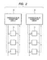
- FIG. 2 is a diagram illustrating a configuration of providing a threshold value correction circuit to each pixel circuit column.
- FIG. 3 is a diagram illustrating the configurations of a pixel circuit and a threshold value correction circuit of an AM type organic EL display apparatus, which is a first exemplary embodiment of the drive circuit of the present invention.
- FIG. 4 is a timing chart illustrating the operation of the pixel circuit of the first exemplary embodiment.
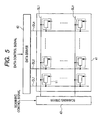
- FIG. 5 is a diagram illustrating the schematic configuration of the whole body of the AM type organic EL display apparatus of the first exemplary embodiment.
- FIG. 6 is a diagram illustrating a data driver and a threshold value correction circuit portion.
- FIG. 7 is a diagram illustrating a D/A converter, the threshold value correction circuit portion, and pixel circuit columns.
- FIG. 8 is a diagram illustrating a circuit configuration of a pixel circuit portion and a threshold value correction circuit (also called compensation circuit) in a threshold value programming period.
- FIG. 9 is a diagram illustrating the circuit configuration in a region in which the connection with a light emitting device is performed.
- FIG. 10 is a diagram illustrating a fifth exemplary embodiment of a drive circuit of a light emitting display apparatus of the present invention.
- FIG. 11 is a diagram illustrating a time chart of the fifth exemplary embodiment.
- FIG. 12 is a diagram illustrating the circuit configuration of a pixel circuit portion and a threshold value correction circuit in a threshold value programming period.
- FIG. 13 is a diagram illustrating the circuit configuration of the pixel circuit portion and the threshold value correction circuit in a light emitting device driving period.
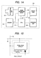
- FIG. 14 is a block diagram of an example of a digital still camera.
- FIG. 15 is a diagram illustrating an arrangement of a pixel circuit in an active matrix type organic EL display apparatus.
- the drive transistors that can be used for the present invention are those having variation of threshold values among the parameters pertaining to electric optical characteristics, or having shift of threshold values as changes of electric optical characteristics owing to electric stresses.
- the present invention corrects the variation of the threshold voltages of the transistors for driving to obtain the stable emission intensity of light emitting devices with the suppressed influences of the threshold voltages of the transistors for driving.
- the light emitting devices the light emitting devices emitting lights having the brightness determined by supplied currents, for example, AM type organic EL devices can be used.
- the drain terminal of a drive transistor is connected to a light emitting device, and the source terminal of the drive transistor is connected to a threshold value correction circuit for correcting the threshold value of the drive transistor.
- Either of a data voltage Vdata and an output from the threshold value correction circuit is input into the gate of the drive transistor, which gate is the control electrode thereof.
- the data voltage Vdata is input into the gate of the drive transistor by turning on a switch in a period before a light emitting device driving period of the light emitting device.
- a voltage of (Vdata - Vth) (Vth denotes a threshold voltage) is input into the threshold value correction circuit, and the threshold value correction circuit inverts the polarity (positive or negative) of the threshold voltage Vth to output a voltage (Vdata + Vth) to the gate of the drive transistor.
- inversion of the polarity (positive and negative) of the above-described threshold voltage Vth will be given.
- the current to be supplied to the light emitting device by the drive transistor during the light emitting device driving period has a value independent of the threshold value Vth of the drive transistor, and the current scarcely receives the influences of the value of the threshold voltage Vth and the changes of the value.
- the threshold value correction circuit may output, for example, a voltage (2V1 - Vdata + Vth) as it will be described in a second exemplary embodiment described below.
- V1 denotes an arbitrary DC voltage
- the threshold value correction circuit is provided to each pixel circuit including a drive transistor, and the threshold value correction circuit and the pixel circuit may constitute a pixel.
- a threshold value correction circuit 31 may be provided to each pixel circuit column, in which a plurality of pixel circuits 11 are arranged.
- FIG. 2 the configuration illustrated in FIG. 2 will be described.
- the configuration of the pixel circuit will be described in the exemplary embodiment described below, but the configuration of the pixel circuit is not limited to that of the exemplary embodiment.
- a field-effect transistor for driving is described as the drive transistor.
- FIG. 3 is a diagram illustrating a pixel circuit and a threshold value correction circuit of an AM type organic EL display apparatus, which are a first exemplary embodiment of the drive circuit of the present invention
- FIG. 4 is a timing chart illustrating the operation of the pixel circuit.
- FIG. 5 is a diagram illustrating the schematic configuration of the whole body of the AM type organic EL display apparatus.
- FIG. 6 is a diagram illustrating a data driver and a threshold value correction circuit portion.
- FIG. 7 is a diagram illustrating a D/A converter, the threshold value correction circuit portion, and pixel circuit columns.
- FIG. 5 does not illustrate the threshold value correction circuit for simplification.
- an AM type organic EL device is used as the light emitting device emitting a light having the brightness determined by a supplied current.
- the AM type organic EL display apparatus includes a pixel region 41 having pixel circuits 11 arranged two-dimensionally in a plane, a data driver 42, and a scanning driver 43.
- the data driver 42 transmits data signals to the respective pixel circuits 11 through data lines DL1-DLn.
- the scanning driver 43 transmits scanning signals through scanning lines SL1-SLn to perform the scanning for each pixel circuit row.
- the data driver 42 includes a shift register, a data register, a data latch circuit, and a D/A converter. As illustrated in FIGS.
- the threshold value correction circuit 31 is provided to each pixel circuit column, and a plurality of threshold value correction circuits 31 are arranged to constitute the threshold value correction circuit portion, which is disposed between the D/A converter and the pixel region 41. That is, the threshold value correction circuits 31 are arranged in the vicinity region of the pixel region 41, in which a plurality of pixel circuits 11 are arranged.
- each of the pixel circuits 11 includes an organic EL device 9, switches SW1-SW6, which are a first switch to a sixth switch, respectively, a drive transistor Tr10, and a capacitor 19.
- Each of the threshold value correction circuits 31 includes a current source (which is a current source circuit) 12, operational amplifiers AMP7 and AMP8, and resistor devices R14 and R15.
- the cathode of the organic EL device 9 is connected to the drain terminal of the N type drive transistor Tr10.
- the data voltage Vdata is input into the gate of the drive transistor Tr10, which is the control electrode thereof, through the fifth switch SW5.
- the output from the threshold value correction circuit 31 is accumulated in the capacitor 19 through the second switch SW2.
- the signal from the threshold value correction circuit 31 is output to the gate of the drive transistor Tr10 by turning off the fifth switch SW5 and by turning on the fourth switch SW4.
- the output terminal of the operational amplifier AMP7 which is a first operational amplifier, is connected to the inversion input terminal of the operational amplifier AMP8, which is a second operational amplifier, through the resistor device R14, which is a first resistor device.
- the non-inversion input terminal of the operational amplifier AMP7 is connected to the source terminal of the drive transistor Tr10 through the first switch SW1, and the inversion input terminal of the operational amplifier AMP7 is connected to its own output terminal.
- the output terminal of the operational amplifier AMP8 is connected to its own inversion input terminal through the resistor device R15.
- the capacitor 19 is connected to the output terminal of the operational amplifier AMP8 through the second switch SW2.
- the third switch SW3 is connected between the source terminal of the drive transistor Tr10 and the ground.
- One of the terminals of each of the fourth switch SW4 and the fifth switch SW5 is connected to the gate terminal of the drive transistor Tr10.
- the other terminal of the fourth switch SW4 is connected to the connection point of the capacitor 19 and the second switch SW2.
- the other terminal of the fifth switch SW5 is connected to the signal line from the data driver 42.
- the sixth switch SW6 is connected to both the terminals of the organic EL device 9 in parallel to the organic EL device 9.
- the transistors and the capacitor 11 in the pixel circuit 11 are formed by an amorphous semiconductor process, and the current source 12, the resistor devices R14 and R15, and the operational amplifiers AMP7 and AMP8 in the threshold value correction circuit 31 are produced by a crystal Si process.
- the data driver section is similarly produced by the crystal Si process.
- the circuit configuration of the present exemplary embodiment uses the first switch SW1 to the sixth switch SW6, and includes a circuit configuration to realize at least two modes of a "threshold value programming period" and a "light emitting device driving period” at the time of image display.
- the timing chart of each switch at that time is illustrated in FIG. 4 .
- P1 denotes the timing of the control signals of the first, second, and sixth switches SW1, SW2, and SW6;
- P2 denotes the timing of the control signal of the fifth switch SW5;
- P3 denotes the timing of the control signal of the third switch SW3; and
- P4 denotes the timing of the control signal of the fourth switch SW4.
- FIG. 8 is a diagram illustrating the circuit configuration of the pixel circuit portion and the threshold value correction circuit 31 in the threshold value programming period.
- the first to the sixth switches SW1-SW6 are opened or closed so that there may be a period in which the first, second, fifth, and sixth switches SW1, SW2, SW5, and SW6 are simultaneously in their on-states and the third and fourth switches SW3 and SW4 are simultaneously in their off-states.
- FIG. 9 is a diagram illustrating the circuit configuration of the region in which the connection with the light emitting device in the light emitting device driving period is performed. As illustrated in FIG. 9 , the switches SW1-SW6 are opened or closed so that there may be a period in which the third and fourth switches SW3 and SW4 are simultaneously in their on-states and the first, second, fifth, and sixth switches SW1, SW2, SW5, and SW6 are simultaneously in their off-states.
- a signal Vdata from the D/A converter of the data driver 42 in Fig.5 is input into the gate of the drive transistor Tr10 having the threshold value Vth and the reference power source Vref13 of the operational amplifier AMP8.
- the drain of the drive transistor Tr10 at this time is connected to the power source, and the source thereof is connected to the current source 12.
- the drive transistor Tr10 and the current source 12 constitutes a source follower circuit, and the source voltage is input into the inversion input terminal of the operational amplifier AMP8, which is an inversion amplifier having the gain of one time, through the operational amplifier AMP7, which is a voltage follower.
- the resistor devices R14 and R15 are set to have the same resistance values.
- the output of the source follower is a node 16
- the output of the voltage follower amplifier is a node 17 in FIG. 8 here
- the electric potential of the node 16 is Vdata - Vth
- the electric potential of the node 17 is Vdata - Vth.
- the gate terminal of the drive transistor Tr10 is isolated from the signal line from the data driver 42, and is connected to the capacitor 19 instead.
- the drain terminal of the drive transistor Tr10 is connected to the cathode of the organic EL device, and the source terminal thereof is connected to the ground.
- the drain current Ids of the drive transistor Tr10 can be expressed here as Ids ⁇ Vgs - Vth 2 where Vgs denotes the gate-to-source voltage thereof.
- drain current Ids can be expressed as Ids ⁇ Vdata 2
- the current supplied from the drive transistor Tr10 to the organic EL device 9 takes a value independent of the threshold value Vth of the drive transistor Tr10, and is scarcely influenced by the value of the threshold value Vth and the changes of the value.
- the present invention can be also applied to a light emitting display apparatus that emits a light based on a supplied current and a current load device using a general current load expressing an arbitrary function base on a supplied current.
- FIGS. 3, 4 , 8, and 9 The configuration of a second exemplary embodiment of the present invention is illustrated in FIGS. 3, 4 , 8, and 9 almost similarly to that of the first exemplary embodiment. However, in the configuration of the second exemplary embodiment, the sixth switch SW6 illustrated in FIG. 3 is removed. One switching device in a pixel region can be hereby reduced in comparison with the configuration of the first exemplary embodiment.
- the organic EL device 9 emits a light based on a supplied current having a parameter of the threshold voltage Vth of the drive transistor Tr10 as expressed by: Ids ⁇ (Vdata - Vth) 2 .
- the threshold value programming period is a sufficiently short period as compared with the normal light emitting device driving period, the influences of the brightness in that period can be neglected when the influences are observed in the entire frame period.
- FIGS. 3, 4 , 8, and 9 The configuration of a third exemplary embodiment of the present invention is illustrated in FIGS. 3, 4 , 8, and 9 almost similarly to that of the first exemplary embodiment. However, in the configuration of the third exemplary embodiment, the current source 12 of the first exemplary embodiment is removed.
- the node 16 takes substantially the electric potential level of (Vdata - Vth), and consequently, almost the same advantages can be obtained by the similar operation to that of the first exemplary embodiment.
- FIGS. 3, 4 , 8, and 9 The configuration of a fourth exemplary embodiment of the present invention can be illustrated by FIGS. 3, 4 , 8, and 9 similarly to that of the first exemplary embodiment.
- the reference power source 13 of the operational amplifier AMP8 which functions as an inversion amplifier, is not the signal from the data driver 42, but a DC power source having another electric potential level.
- the supplied current to the organic EL device 9 is scarcely influenced by the value of the threshold voltage Vth and the changes of the value similarly to that of the first exemplary embodiment.
- FIG. 10 A fifth exemplary embodiment of a drive circuit of the light emitting display apparatus of the present invention is illustrated in FIG. 10 .
- the configuration of the fifth exemplary embodiment differs from that illustrated in FIG. 3 in that a capacitor 20 is provided and the switch SW5 are removed, and in that the data signal Vdata is input into the gate of the drive transistor Tr10, which is the control electrode thereof, through the fourth switch SW4.
- the capacitor 20 is shown here to generally express the parasitic capacitance components of the wiring from the data driver 42 to the second switch SW2 in the pixel and the switching transistors connected to the wiring.
- the circuit configuration of the present exemplary embodiment includes a circuit configuration for realizing at least two modes of the "threshold value programming period" and the "light emitting device driving period” at the time of image display similarly to that of the first exemplary embodiment.
- the timing chart of each switch at that time is illustrated in FIG. 11 .
- FIG. 12 is a diagram illustrating the circuit configuration of the pixel circuit portion and the threshold value correction circuit 31 in the threshold value programming period. As illustrated in FIG. 12 , the switches are opened or closed so that there may be a period in which the first, fourth, and sixth switches SW1, SW4, and SW6 are simultaneously in their on-states and the second and third switches SW2 and SW3 are simultaneously in their off-states.
- the first, fourth, and sixth switches SW1, SW4, and SW6 are turned to be in their off-states, and the second switch SW2 is turned to be in its on-states. Thereby, the charges of the capacitor device 20 are moved to the capacitor 19.
- the second switch SW2 is turned to be in its off-state, and the third switch SW3 is turned to be in its on-state.
- the capacitor 19 is connected to the gate terminal of the drive transistor Tr10; the organic light emitting device 9 is connected to the drain terminal of the drive transistor Tr10; and the source terminal of the drive transistor Tr10 is connected to the ground.
- the operation of the fifth exemplary embodiment is similar to that of the first exemplary embodiment. However, as illustrated in FIG. 12 , the electric potential of the node 18 is accumulated in the capacitor 20. In this period, the organic EL device 9 does not emit any lights.
- the terminal of the capacitor 19 is first isolated from the signal line from the data driver 42, and is connected to the capacitor 20 instead, by turning the switch SW2 to be in its on-state and by turning the switch SW4 to be in its off-sate.
- the switch SW2 is turned to be in its off-state, and the charges of the capacitor 20 have moved to the capacitor 19.
- the gate terminal of the drive transistor Tr10 is held by the capacitor 19 to be the voltage (Vdata + Vth).
- the drain terminal of the drive transistor Tr10 is connected to the cathode of the organic EL device 9, and the source terminal thereof is connected to the ground.
- the drain current Ids of the drive transistor Tr10 may be expressed here similarly in the first exemplary embodiment as Ids ⁇ Vdata 2
- the current supplied from the drive transistor Tr10 to the organic EL device 9 takes a value independent of the threshold value Vth of the drive transistor Tr10, and is scarcely influenced by the changes of the value of the threshold voltage Vth.
- the number of the switches in a pixel can be reduced by one as compared with six of the first exemplary embodiment.
- the present exemplary embodiment can operated with four switches in a pixel.
- the AM type organic EL display apparatus of each of the aforesaid exemplary embodiments may configure an information display apparatus.
- the information display apparatus is used in a cellar phone, a portable computer, a camera such as a still camera and a video camera, and an apparatus realizing their plural functions.
- FIG. 14 is a block diagram illustrating an example of a digital still camera.
- the entire system 129 includes a photographing unit 123 for picking up an object image, an image signal processing circuit (which is an image signal processing unit) 124, a display panel 125, a memory 126, a CPU 127, and an operation unit 128.
- An image photographed by the photographing unit 123 or an image recorded in a memory 126 is subjected to the signal processing by the image signal processing circuit 124, and the image can be observed on the display panel 125.
- the CPU 127 controls the photographing unit 123, the memory 126, and the image signal processing circuit 124 based on an input from the operation unit 128 to perform photographing, recording, reproducing, and displaying suitable to a situation.
Landscapes
- Engineering & Computer Science (AREA)
- Physics & Mathematics (AREA)
- Computer Hardware Design (AREA)
- General Physics & Mathematics (AREA)
- Theoretical Computer Science (AREA)
- Control Of Indicators Other Than Cathode Ray Tubes (AREA)
- Control Of El Displays (AREA)
- Electroluminescent Light Sources (AREA)
Applications Claiming Priority (1)
| Application Number | Priority Date | Filing Date | Title |
|---|---|---|---|
| JP2007061871A JP5566000B2 (ja) | 2007-03-12 | 2007-03-12 | 発光表示装置の駆動回路、その駆動方法並びにカメラ |
Publications (2)
| Publication Number | Publication Date |
|---|---|
| EP1970883A2 true EP1970883A2 (de) | 2008-09-17 |
| EP1970883A3 EP1970883A3 (de) | 2009-12-16 |
Family
ID=39552732
Family Applications (1)
| Application Number | Title | Priority Date | Filing Date |
|---|---|---|---|
| EP08002641A Withdrawn EP1970883A3 (de) | 2007-03-12 | 2008-02-13 | Ansteuerung und Ansteuerungsverfahren für lichtemittierende Anzeigevorrichtungen |
Country Status (6)
| Country | Link |
|---|---|
| US (2) | US8009157B2 (de) |
| EP (1) | EP1970883A3 (de) |
| JP (1) | JP5566000B2 (de) |
| KR (1) | KR100966502B1 (de) |
| CN (1) | CN101266751B (de) |
| TW (1) | TWI390488B (de) |
Families Citing this family (11)
| Publication number | Priority date | Publication date | Assignee | Title |
|---|---|---|---|---|
| JP2010002498A (ja) * | 2008-06-18 | 2010-01-07 | Sony Corp | パネルおよび駆動制御方法 |
| JP5676945B2 (ja) | 2010-07-08 | 2015-02-25 | キヤノン株式会社 | 電子装置、電子装置の素子分離方法、電子装置の製造方法、及び電子装置を備えた表示装置 |
| JP6124573B2 (ja) * | 2011-12-20 | 2017-05-10 | キヤノン株式会社 | 表示装置 |
| TWI682632B (zh) * | 2014-12-26 | 2020-01-11 | 日商半導體能源研究所股份有限公司 | 半導體裝置 |
| CN109644243B (zh) * | 2018-11-20 | 2020-11-24 | 深圳市汇顶科技股份有限公司 | 像素电路及相关影像感测器 |
| CN110503920B (zh) * | 2019-08-29 | 2021-02-23 | 云谷(固安)科技有限公司 | 一种显示装置及其驱动方法 |
| KR102736770B1 (ko) * | 2019-12-30 | 2024-11-29 | 엘지디스플레이 주식회사 | 표시 장치 및 표시 장치의 구동 방법 |
| KR102289926B1 (ko) * | 2020-05-25 | 2021-08-19 | 주식회사 사피엔반도체 | 디스플레이 밝기 제어 장치 |
| US11462162B1 (en) * | 2021-06-01 | 2022-10-04 | Sharp Display Technology Corporation | High current active matrix pixel architecture |
| CN114067728B (zh) * | 2021-10-18 | 2023-04-07 | 浙江大学 | 一种静态阈值电压补偿电路 |
| CN117198221B (zh) * | 2023-11-07 | 2024-02-06 | 上海视涯技术有限公司 | 一种数据存储电路、硅基显示面板及显示装置 |
Citations (1)
| Publication number | Priority date | Publication date | Assignee | Title |
|---|---|---|---|---|
| US6809706B2 (en) | 2001-08-09 | 2004-10-26 | Nec Corporation | Drive circuit for display device |
Family Cites Families (18)
| Publication number | Priority date | Publication date | Assignee | Title |
|---|---|---|---|---|
| US4856090A (en) | 1984-05-22 | 1989-08-08 | Canon Kabushiki Kaisha | Light communication equipment |
| DE69328230T2 (de) | 1992-12-01 | 2000-08-10 | Canon K.K., Tokio/Tokyo | Entfernungbildverarbeitungsvorrichtung und -verfahren |
| US5952789A (en) | 1997-04-14 | 1999-09-14 | Sarnoff Corporation | Active matrix organic light emitting diode (amoled) display pixel structure and data load/illuminate circuit therefor |
| CN1201280C (zh) | 2000-05-22 | 2005-05-11 | 皇家菲利浦电子有限公司 | 有源矩阵电致发光显示设备 |
| JP4069437B2 (ja) * | 2000-12-15 | 2008-04-02 | 富士フイルム株式会社 | 携帯端末、店頭端末、通信システム及び通信方法 |
| JP2003224767A (ja) * | 2002-01-29 | 2003-08-08 | Fuji Photo Film Co Ltd | 撮像装置、主要被写体位置決定方法、及びプログラム |
| JP2003280588A (ja) * | 2002-03-20 | 2003-10-02 | Sanyo Electric Co Ltd | 携帯型電話機 |
| KR20050057388A (ko) * | 2002-09-18 | 2005-06-16 | 코닌클리케 필립스 일렉트로닉스 엔.브이. | 패시브 매트릭스 자가 방출 디스플레이 소자용 구동 장치 |
| JP3832415B2 (ja) | 2002-10-11 | 2006-10-11 | ソニー株式会社 | アクティブマトリクス型表示装置 |
| JP4378087B2 (ja) * | 2003-02-19 | 2009-12-02 | 奇美電子股▲ふん▼有限公司 | 画像表示装置 |
| JP2007506145A (ja) * | 2003-09-23 | 2007-03-15 | イグニス イノベーション インコーポレーテッド | 発光ピクセルのアレイを駆動する回路及び方法 |
| CA2443206A1 (en) * | 2003-09-23 | 2005-03-23 | Ignis Innovation Inc. | Amoled display backplanes - pixel driver circuits, array architecture, and external compensation |
| JP2005321433A (ja) * | 2004-05-06 | 2005-11-17 | Mitsubishi Electric Corp | 画像表示装置およびその検査方法 |
| JP4081462B2 (ja) * | 2004-08-02 | 2008-04-23 | 沖電気工業株式会社 | 表示パネルの色合い調整回路 |
| TWI237913B (en) | 2004-10-13 | 2005-08-11 | Chi Mei Optoelectronics Corp | Circuit and method for OLED with voltage compensation abstract of the invention |
| FR2884639A1 (fr) * | 2005-04-14 | 2006-10-20 | Thomson Licensing Sa | Panneau d'affichage d'images a matrice active, dont les emetteurs sont alimentes par des generateurs de courant pilotables en tension |
| JP2006313412A (ja) * | 2005-05-06 | 2006-11-16 | Oki Electric Ind Co Ltd | 電流駆動回路 |
| TWI317925B (en) * | 2005-08-19 | 2009-12-01 | Toppoly Optoelectronics Corp | An active matrix organic light emitting diodes pixel circuit |
-
2007
- 2007-03-12 JP JP2007061871A patent/JP5566000B2/ja not_active Expired - Fee Related
-
2008
- 2008-02-08 US US12/028,588 patent/US8009157B2/en not_active Expired - Fee Related
- 2008-02-13 EP EP08002641A patent/EP1970883A3/de not_active Withdrawn
- 2008-02-21 TW TW097106086A patent/TWI390488B/zh not_active IP Right Cessation
- 2008-03-12 KR KR1020080022701A patent/KR100966502B1/ko not_active Expired - Fee Related
- 2008-03-12 CN CN2008100835797A patent/CN101266751B/zh not_active Expired - Fee Related
-
2011
- 2011-04-13 US US13/086,226 patent/US8610695B2/en not_active Expired - Fee Related
Patent Citations (1)
| Publication number | Priority date | Publication date | Assignee | Title |
|---|---|---|---|---|
| US6809706B2 (en) | 2001-08-09 | 2004-10-26 | Nec Corporation | Drive circuit for display device |
Also Published As
| Publication number | Publication date |
|---|---|
| TW200903418A (en) | 2009-01-16 |
| KR20080083598A (ko) | 2008-09-18 |
| CN101266751A (zh) | 2008-09-17 |
| US8009157B2 (en) | 2011-08-30 |
| KR100966502B1 (ko) | 2010-06-29 |
| EP1970883A3 (de) | 2009-12-16 |
| JP5566000B2 (ja) | 2014-08-06 |
| TWI390488B (zh) | 2013-03-21 |
| US8610695B2 (en) | 2013-12-17 |
| US20110187888A1 (en) | 2011-08-04 |
| JP2008224958A (ja) | 2008-09-25 |
| US20080225023A1 (en) | 2008-09-18 |
| CN101266751B (zh) | 2011-01-19 |
Similar Documents
| Publication | Publication Date | Title |
|---|---|---|
| US8610695B2 (en) | Drive circuit and drive method of light emitting display apparatus | |
| CN100520883C (zh) | 图像显示装置 | |
| US7109952B2 (en) | Light emitting display, light emitting display panel, and driving method thereof | |
| KR101089050B1 (ko) | 반도체 장치 | |
| US20060221009A1 (en) | Drive circuit for electroluminescent device | |
| JP4504926B2 (ja) | 有機電界発光表示装置及びその動作方法 | |
| JP2010249955A (ja) | 表示装置 | |
| US7663575B2 (en) | Driving circuit for driving organic electroluminescent element, display panel and display apparatus having the same | |
| WO2010041426A1 (ja) | 画像表示装置およびその制御方法 | |
| KR100610711B1 (ko) | 표시 장치 | |
| US7920120B2 (en) | Display device, driving method of the same and electronic equipment having the same | |
| WO2006103797A1 (ja) | 表示装置およびその駆動方法 | |
| JP2001042826A (ja) | アクティブマトリクス型発光パネル及び表示装置 | |
| KR101457035B1 (ko) | 표시 장치 및 그의 구동 방법 | |
| KR100556180B1 (ko) | 표시 회로 | |
| EP1580719A1 (de) | Anzeige, aktivmatrixsubstrat und ansteuerverfahren | |
| KR101502070B1 (ko) | 표시 장치 및 그의 구동 방법 | |
| US7573442B2 (en) | Display, active matrix substrate, and driving method | |
| US20060202919A1 (en) | Display, array substrate, and method of driving display | |
| JP5570644B2 (ja) | 発光表示装置の駆動回路 | |
| KR102888465B1 (ko) | 전계 발광 표시장치 | |
| JP4044537B2 (ja) | 表示装置及びその駆動方法 | |
| KR20190053688A (ko) | 유기 발광 표시장치 | |
| KR100581806B1 (ko) | 발광 표시장치 및 데이터 구동부 |
Legal Events
| Date | Code | Title | Description |
|---|---|---|---|
| PUAI | Public reference made under article 153(3) epc to a published international application that has entered the european phase |
Free format text: ORIGINAL CODE: 0009012 |
|
| AK | Designated contracting states |
Kind code of ref document: A2 Designated state(s): AT BE BG CH CY CZ DE DK EE ES FI FR GB GR HR HU IE IS IT LI LT LU LV MC MT NL NO PL PT RO SE SI SK TR |
|
| AX | Request for extension of the european patent |
Extension state: AL BA MK RS |
|
| PUAL | Search report despatched |
Free format text: ORIGINAL CODE: 0009013 |
|
| AK | Designated contracting states |
Kind code of ref document: A3 Designated state(s): AT BE BG CH CY CZ DE DK EE ES FI FR GB GR HR HU IE IS IT LI LT LU LV MC MT NL NO PL PT RO SE SI SK TR |
|
| AX | Request for extension of the european patent |
Extension state: AL BA MK RS |
|
| 17P | Request for examination filed |
Effective date: 20100616 |
|
| AKX | Designation fees paid |
Designated state(s): AT BE BG CH CY CZ DE DK EE ES FI FR GB GR HR HU IE IS IT LI LT LU LV MC MT NL NO PL PT RO SE SI SK TR |
|
| 17Q | First examination report despatched |
Effective date: 20110510 |
|
| STAA | Information on the status of an ep patent application or granted ep patent |
Free format text: STATUS: THE APPLICATION HAS BEEN WITHDRAWN |
|
| 18W | Application withdrawn |
Effective date: 20130527 |