EP1968188B1 - Klasse-D Verstärkeranordnung - Google Patents
Klasse-D Verstärkeranordnung Download PDFInfo
- Publication number
- EP1968188B1 EP1968188B1 EP07004878A EP07004878A EP1968188B1 EP 1968188 B1 EP1968188 B1 EP 1968188B1 EP 07004878 A EP07004878 A EP 07004878A EP 07004878 A EP07004878 A EP 07004878A EP 1968188 B1 EP1968188 B1 EP 1968188B1
- Authority
- EP
- European Patent Office
- Prior art keywords
- amplifier arrangement
- arrangement according
- switching elements
- bypass capacitor
- bridge
- Prior art date
- Legal status (The legal status is an assumption and is not a legal conclusion. Google has not performed a legal analysis and makes no representation as to the accuracy of the status listed.)
- Active
Links
Images
Classifications
-
- H—ELECTRICITY
- H03—ELECTRONIC CIRCUITRY
- H03F—AMPLIFIERS
- H03F3/00—Amplifiers with only discharge tubes or only semiconductor devices as amplifying elements
- H03F3/20—Power amplifiers, e.g. Class B amplifiers, Class C amplifiers
- H03F3/21—Power amplifiers, e.g. Class B amplifiers, Class C amplifiers with semiconductor devices only
- H03F3/217—Class D power amplifiers; Switching amplifiers
-
- H—ELECTRICITY
- H01—ELECTRIC ELEMENTS
- H01J—ELECTRIC DISCHARGE TUBES OR DISCHARGE LAMPS
- H01J37/00—Discharge tubes with provision for introducing objects or material to be exposed to the discharge, e.g. for the purpose of examination or processing thereof
- H01J37/32—Gas-filled discharge tubes
- H01J37/32009—Arrangements for generation of plasma specially adapted for examination or treatment of objects, e.g. plasma sources
- H01J37/32082—Radio frequency generated discharge
- H01J37/32174—Circuits specially adapted for controlling the RF discharge
-
- H—ELECTRICITY
- H05—ELECTRIC TECHNIQUES NOT OTHERWISE PROVIDED FOR
- H05H—PLASMA TECHNIQUE; PRODUCTION OF ACCELERATED ELECTRICALLY-CHARGED PARTICLES OR OF NEUTRONS; PRODUCTION OR ACCELERATION OF NEUTRAL MOLECULAR OR ATOMIC BEAMS
- H05H1/00—Generating plasma; Handling plasma
- H05H1/24—Generating plasma
- H05H1/26—Plasma torches
- H05H1/32—Plasma torches using an arc
- H05H1/34—Details, e.g. electrodes, nozzles
- H05H1/36—Circuit arrangements
-
- H—ELECTRICITY
- H05—ELECTRIC TECHNIQUES NOT OTHERWISE PROVIDED FOR
- H05H—PLASMA TECHNIQUE; PRODUCTION OF ACCELERATED ELECTRICALLY-CHARGED PARTICLES OR OF NEUTRONS; PRODUCTION OR ACCELERATION OF NEUTRAL MOLECULAR OR ATOMIC BEAMS
- H05H1/00—Generating plasma; Handling plasma
- H05H1/24—Generating plasma
- H05H1/46—Generating plasma using applied electromagnetic fields, e.g. high frequency or microwave energy
-
- H—ELECTRICITY
- H10—SEMICONDUCTOR DEVICES; ELECTRIC SOLID-STATE DEVICES NOT OTHERWISE PROVIDED FOR
- H10W—GENERIC PACKAGES, INTERCONNECTIONS, CONNECTORS OR OTHER CONSTRUCTIONAL DETAILS OF DEVICES COVERED BY CLASS H10
- H10W44/00—Electrical arrangements for controlling or matching impedance
- H10W44/601—Capacitive arrangements
-
- H—ELECTRICITY
- H10—SEMICONDUCTOR DEVICES; ELECTRIC SOLID-STATE DEVICES NOT OTHERWISE PROVIDED FOR
- H10W—GENERIC PACKAGES, INTERCONNECTIONS, CONNECTORS OR OTHER CONSTRUCTIONAL DETAILS OF DEVICES COVERED BY CLASS H10
- H10W90/00—Package configurations
-
- H—ELECTRICITY
- H10—SEMICONDUCTOR DEVICES; ELECTRIC SOLID-STATE DEVICES NOT OTHERWISE PROVIDED FOR
- H10W—GENERIC PACKAGES, INTERCONNECTIONS, CONNECTORS OR OTHER CONSTRUCTIONAL DETAILS OF DEVICES COVERED BY CLASS H10
- H10W72/00—Interconnections or connectors in packages
- H10W72/50—Bond wires
- H10W72/541—Dispositions of bond wires
- H10W72/547—Dispositions of multiple bond wires
- H10W72/5475—Dispositions of multiple bond wires multiple bond wires connected to common bond pads at both ends of the wires
-
- H—ELECTRICITY
- H10—SEMICONDUCTOR DEVICES; ELECTRIC SOLID-STATE DEVICES NOT OTHERWISE PROVIDED FOR
- H10W—GENERIC PACKAGES, INTERCONNECTIONS, CONNECTORS OR OTHER CONSTRUCTIONAL DETAILS OF DEVICES COVERED BY CLASS H10
- H10W72/00—Interconnections or connectors in packages
- H10W72/851—Dispositions of multiple connectors or interconnections
- H10W72/874—On different surfaces
- H10W72/884—Die-attach connectors and bond wires
-
- H—ELECTRICITY
- H10—SEMICONDUCTOR DEVICES; ELECTRIC SOLID-STATE DEVICES NOT OTHERWISE PROVIDED FOR
- H10W—GENERIC PACKAGES, INTERCONNECTIONS, CONNECTORS OR OTHER CONSTRUCTIONAL DETAILS OF DEVICES COVERED BY CLASS H10
- H10W90/00—Package configurations
- H10W90/701—Package configurations characterised by the relative positions of pads or connectors relative to package parts
- H10W90/751—Package configurations characterised by the relative positions of pads or connectors relative to package parts of bond wires
- H10W90/753—Package configurations characterised by the relative positions of pads or connectors relative to package parts of bond wires between laterally-adjacent chips
-
- H—ELECTRICITY
- H10—SEMICONDUCTOR DEVICES; ELECTRIC SOLID-STATE DEVICES NOT OTHERWISE PROVIDED FOR
- H10W—GENERIC PACKAGES, INTERCONNECTIONS, CONNECTORS OR OTHER CONSTRUCTIONAL DETAILS OF DEVICES COVERED BY CLASS H10
- H10W90/00—Package configurations
- H10W90/701—Package configurations characterised by the relative positions of pads or connectors relative to package parts
- H10W90/751—Package configurations characterised by the relative positions of pads or connectors relative to package parts of bond wires
- H10W90/754—Package configurations characterised by the relative positions of pads or connectors relative to package parts of bond wires between a chip and a stacked insulating package substrate, interposer or RDL
Definitions
- the invention relates to an HF class D amplifier arrangement which is suitable for operation at supply voltages ⁇ 100 V and at output powers ⁇ 1 kW, with a half bridge formed by two series-connected switching elements, in particular MOSFETs, with two supply voltage connections and one between the switching elements Output terminal, wherein a bypass capacitor is provided parallel to the series connection of the switching elements.
- High-frequency is usually used when the signal propagation time of a signal from point A to point B on a track is in the range of the period of the signal. This condition is given for frequencies ⁇ 3 MHz. Radio frequency in the sense of the invention thus means frequencies ⁇ 3 MHz. At high frequency, trace lengths and texture play an essential role. It can no longer be assumed that a signal at point 1 adjacent to the same time is also applied at point 2, which is a few centimeters away, and is connected to a conductor track. Rather, the signal is only a few seconds later and may have changed its value under some circumstances. Therefore, own technologies are necessary for such frequencies ⁇ 3 MHz. Technologies known for lower frequencies are not transferable to the frequency range in which the present invention moves.
- Class A and B amplifiers which have the disadvantage of high power loss
- Class D or Class E amplifiers especially RF generators with one or more switching elements
- the class E amplifier has the disadvantage that the voltages on the switching elements formed as transistors increase to over three times the DC supply voltages, while the bridge-formed class-D amplifier limits the voltages at the transistors to the supply voltage.
- the class D amplifier two series connected switching elements, e.g. MOSFETs, used.
- This amplifier arrangement is often referred to as a half-bridge.
- the usual circuit is as follows:
- the upper transistor or switch (High Side Switch, HSS) located at the positive DC supply voltage is connected with its drain connection to the positive DC supply voltage (+ V) and with its source connection to the drain of the lower transistor or switch (LSS).
- the source terminal of the lower transistor is connected to the negative DC supply voltage (-V).
- the output of the half-bridge is tapped between the two switching elements (source from the top and drain from the bottom MOSFET). Both transistors are controlled via their gate connection (control connection).
- the Advanced Power Technology MOSFET Driver Hybrid DRF 1200 is a MOSFET with an integrated driver chip.
- the object of the present invention is to provide an amplifier arrangement suitable for high frequencies.
- All switching elements have an output capacitance (output capacitance in MOSFETs: drain-source capacitance Coss), which is not negligible in high-frequency applications.
- output capacitance in MOSFETs drain-source capacitance Coss
- a MOSFET must discharge its own drain-source capacitance through its R DSON conduction resistor, consuming power (1/2 CU 2 ).
- the half-bridge it must recharge the drain-source capacitance of the other MOSFET, which is locked at this time, while also exciting a swing between the capacitance of the MOSFET and the inductance of the lead.
- the MOSFETs of the half-bridge in high-frequency switching operation and high operating voltage necessarily turn off the power. This is achieved by an inductive portion of the load impedance which, when one MOSFET turns off, still allows enough current to flow to reload the capacitances of the MOSFET to the opposite potential before the other MOSFET turns on.
- switching discharge zero voltage switching
- ZVS zero voltage switching
- the current path from the positive supply voltage across the two transistors to the negative supply voltage is called the load current path.
- the so-called parasitic current path This consists essentially of the so-called bypass capacitor between the positive supply voltage and the negative supply voltage. It serves to avoid voltage drops in the supply voltage at the current pulses occurring in the switching transistors in the switching. It also prevents the destruction of the transistors due to current spikes.
- parts of the load current path and parts of the parasitic current path become a current path (Loop), which contains the switching transistors and the bypass capacitor. Supply lines from the supply voltage connections are not part of this current path.
- This current path has lead inductances and capacitances, eg the output capacitance of the MOSFETs (Coss), and thus forms a resonant circuit.
- This resonant circuit is excited by the switching on and off of the transistors.
- This resonant circuit When this resonant circuit is excited, eg when the zero voltage switching can no longer be achieved, it usually oscillates at significantly higher frequencies (eg 80 MHz) than the fundamental frequency (eg 13.56 MHz). These vibrations are undesirable in the plasma process and also interfere with the function and safety of the RF generator in which the half-bridge is used.
- a meaningful damping of the resonant circuit is associated with power loss, which is extremely undesirable for this high power range.
- both transistors must never be in the conductive state at the same time, otherwise the supply voltage would be short-circuited. That's rising Frequency increasingly difficult to ensure.
- Decisive for the switching on and off of the transistors is the voltage at the gate of the transistors.
- the gate has capacitances to source and drain. If the voltage at the gate terminal of the transistor is now set to a level which is intended to cause the transistor to be switched on or off, then this voltage is only really at the gate after a recharging time, which is dependent on the gate capacitances and connection inductances effective. Since these gate capacitances and lead inductances tend to oscillate, it is customary in the prior art to also provide resistors for damping. This additionally increases the reloading times.
- the specimen scattering of the individual transistors is a problem, which is why transistors are often measured and selected for use in bridge circuits.
- the recharge time varies from transistor to transistor. The time differences are often in a time range that can not be ignored at high frequencies. The synchronization of the transistors is difficult.
- the capacitances in the current path resulting from the load current circuit and the parasitic current path are connected in series, that is to say the total capacitance is determined essentially by the smallest capacitances. These are the output capacitances in the transistors. These can not be reduced arbitrarily. They are determined by the area of the transistors, which in turn depends on the current carrying capacity and thus ultimately on the power that should be able to switch the half-bridge.
- the amplifier arrangement is designed to be particularly low induction. As a result, the unwanted vibrations that occur when a zero voltage switching is not possible because of a changing load, moved to high frequencies that can be damped easier, and certainly can no longer arise by limiting the switching speed of the switching elements.
- the amplifier arrangement according to the invention is particularly suitable for use in HF generators for power over 1kW with supply voltages over 100V and frequencies ⁇ 3 MHz.
- the half-bridge and the bypass capacitor are arranged on an area ⁇ 30 cm 2 , inductances in the current path can be kept so low that disturbing parasitic oscillations are avoided or shifted to such high frequencies that they no longer disturb or simply attenuate them can be.
- the local concentration of the resonant circuit reduces its influence on other circuits, in particular on the clock signal generation.
- the (parasitic) oscillating circuit formed by capacitances and inductances in the current path through the half-bridge and the bypass capacitor has a resonant frequency ⁇ 100 MHz, the resonant frequency resulting from mismatching can be easily damped. Since the capacitance Coss remains the same, a higher resonant frequency means that a higher discharge current occurs earlier, which in turn leads to increased ohmic damping (ohmic losses).
- the connecting lines between the bypass capacitor and the switching elements and between the switching elements each have a length ⁇ 10mm, preferably ⁇ 5mm, more preferably ⁇ 3mm, the switching elements are particularly low inductively hard wired together.
- Connecting lines are understood here as part of the connecting lines. The short lines cause a shortening of the current path through the two switching elements and the parallel bypass capacitor and thus a reduction of the inductances.
- the connecting lines can be made flat, for example a connecting line can be used as a surface, e.g. be designed as copper track, or by many parallel lines in about as wide as long.
- the width and length of the connecting lines, wherein the width can be determined by a plurality of parallel-guided individual connection lines, so are of the same order of magnitude.
- the length and width of the connecting lines correspond. This reduces the inductance of the conductor track.
- At least one driver arrangement may be provided, which is connected to the control terminals of the switching elements, wherein the connecting lines of the driver arrangement to the switching elements have a length ⁇ 10mm, preferably ⁇ 5mm, more preferably ⁇ 3mm.
- the inductances in the connecting lines can also be reduced, so that a low-inductance connection of the driver arrangement is also possible.
- the driver arrangement is located closer to the switching elements, in particular the gates of the MOSFETs, the MOSFETs are less susceptible to the Miller feedback of the oscillation in the parasitic resonant circuit.
- the half-bridge and the bypass capacitor may be arranged on a common substrate.
- the Drivers for the transistors are arranged according to the invention on the substrate.
- the semiconductor devices are applied directly to the substrate and directly connected (bonded) to interconnection line sections located in, on, or on the substrate.
- Both MOSFETs and drivers are designed as semiconductor components. Since a plurality of connecting wires (bonding wires) are laid in parallel from the semiconductor components to the connecting line sections, the connection is particularly low in inductance.
- the connecting lines together with the connecting line sections represent connecting lines.
- the connecting lines can also be wired (bonded) directly from semiconductor module to semiconductor module.
- Connection lines can be constructed on, in or on the substrate particularly low induction. If the semiconductor wiring components are housed in a closed housing, shorter safety distances can be realized without the risk of flashovers, because the risk of contamination is lower and thus minimum creepage distances can be realized shorter. If the wired semiconductor devices are encapsulated in a housing, even shorter safety distances can be realized without the risk of flashovers, because now instead of creepage distances insulation coordinates of the potting compound can be considered.
- a particularly space-saving arrangement with short current path and short connecting lines between the components is obtained if at least the half-bridge and the bypass capacitor are integrated in a semiconductor module.
- the switching elements are arranged on a heat sink.
- the heat sink may be formed as a cooling plate or multilayer board. If the heat sink is made of ceramic, it can dissipate the heat particularly well.
- the connecting lines between the bypass capacitor and the switching elements can be kept short and thus the line inductances can be kept low if the bypass capacitor is arranged above or below the switching elements.
- bypass capacitor is formed as a substrate for the switching elements, extremely short connecting lines can be realized.
- the bypass capacitor in this case can also serve as a heat sink for the switching elements.
- a module in the sense of the invention is an assembly which represents a unit and as such can be installed, for example, in an HF generator.
- the module has no connection to the heat sink.
- the module is electrically insulated from the heat sink.
- connection pins or connection lugs are arranged as connection pins or connection lugs on the side opposite the heat sink.
- connection lugs offer a lower resistance for high-frequency currents than cables with a round cross-section.
- the amplifier arrangement for good thermal conductivity can be arranged directly on the heat sink without additional electrical insulation plates.
- the terminals can be connected to a printed circuit board, which is arranged above the modules, in particular soldered thereto.
- An advantageous embodiment is characterized in that two capacitors connected in series are provided between the supply voltage terminals.
- a midpoint between a positive supply voltage + V and the negative supply voltage -V can be generated.
- these capacitors are also low induction, i. with short connecting cables, connected.
- they are arranged in the module.
- the lines to the capacitors have a length ⁇ 10 mm, preferably ⁇ 5 mm, especially preferably have ⁇ 3mm. By this measure, these capacitors are connected with low induction.
- Such a low-inductance compound results in particular in that the connecting line of the heat sink to ground has a length ⁇ 10 mm, preferably ⁇ 5 mm, particularly preferably ⁇ 3 mm.
- the scope of the invention also includes an RF generator with an amplifier arrangement as described above.
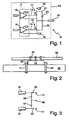
- the FIG. 1 shows an RF class D amplifier arrangement 10, which comprises two series-connected designed as MOSFETs switching elements 11,12, which form a half-bridge.
- the control terminals 13, 14 of the switching elements 11, 12 are each driven by a driver module 15, 16 of a driver arrangement 17.
- the upper switching element 11 is connected to a positive supply voltage 18 and the lower switching element 12 to a negative supply voltage 19.
- Between the switching elements 11, 12 is the output terminal 24th
- a bypass capacitor 20 Parallel to the switching elements 11,12 and between the positive and negative supply voltage 18,19 a bypass capacitor 20 is designed.
- the connection between the switching elements 11,12 and the connecting lines 21,22 to the bypass capacitor 20 are formed induction poor. This means that they are as short as possible. In particular, this also makes the current path through the switching elements 12, 13 and the bypass capacitor 20 very short.
- the entire amplifier arrangement 10 is arranged in a housing 23.
- the amplifier arrangement 10 in particular its switching elements 11, 12 is arranged on a heat sink 30 and screwed thereto by means of screws 31,32.
- a ground connection of the amplifier assembly 10 is made with the heat sink 30.
- Connection pins 33 of the amplifier arrangement 10 are brought up out of the housing 23, so that they can be connected to a printed circuit board 34, which is arranged above the amplifier arrangement 10.
- capacitors 36, 37 are shown, which are connected between the positive supply voltage 18 and the negative supply voltage 19. Through them, a center 38 (center potential) between the supply voltages 18,19 realized. Furthermore, capacitors 39, 40 are provided between the supply voltages 18, 19 and ground 41. The mass 41 may be low inductively connected to the heat sink 30.
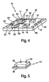
- the switching elements 11, 12 are each designed as semiconductor components (dice) and arranged on a substrate 50, which can serve as a heat sink.
- the switching elements 11, 12 sit with their drain D1, D2 respectively on the substrate 50 and are contacted from below.
- the source connection S1, S2 is located at the top.
- the source terminals S1, S2 are connected via connecting lines 51, 52, which are designed as bonding wires, with connecting line sections extending in the substrate.
- the connecting lines 51, 52 are also kept as short as possible and can be considered as part of the connecting lines between components.
- the bypass capacitor 20 is also disposed on the substrate 50.
- the gate terminals (control terminals) G1, G2 are also overhead and via connecting lines 53, 54, which are also designed as bonding wires, with arranged on the substrate 50 driver chips 15, 16 connected.
- the capacitors 36, 37 are also arranged on the substrate 50. Connecting pins 33 and terminal lugs protrude from the substrate 50, in which inter alia the connecting lines 21, 22 extend.
- the substrate has fastening means 55 - here through-holes - for fixing the substrate 50.
- the amplifier arrangement 10 is arranged in a housing 60 on a substrate 50.
- the connection pins 33 protrude upward from the housing 60.
Landscapes
- Physics & Mathematics (AREA)
- Engineering & Computer Science (AREA)
- Plasma & Fusion (AREA)
- Chemical & Material Sciences (AREA)
- Analytical Chemistry (AREA)
- Spectroscopy & Molecular Physics (AREA)
- Power Engineering (AREA)
- Electromagnetism (AREA)
- Amplifiers (AREA)
- Plasma Technology (AREA)
Priority Applications (3)
| Application Number | Priority Date | Filing Date | Title |
|---|---|---|---|
| EP07004878A EP1968188B1 (de) | 2007-03-09 | 2007-03-09 | Klasse-D Verstärkeranordnung |
| US12/044,572 US7705676B2 (en) | 2007-03-09 | 2008-03-07 | Class D amplifier arrangement |
| JP2008059620A JP5675033B2 (ja) | 2007-03-09 | 2008-03-10 | D級増幅装置 |
Applications Claiming Priority (1)
| Application Number | Priority Date | Filing Date | Title |
|---|---|---|---|
| EP07004878A EP1968188B1 (de) | 2007-03-09 | 2007-03-09 | Klasse-D Verstärkeranordnung |
Publications (2)
| Publication Number | Publication Date |
|---|---|
| EP1968188A1 EP1968188A1 (de) | 2008-09-10 |
| EP1968188B1 true EP1968188B1 (de) | 2012-08-08 |
Family
ID=38123951
Family Applications (1)
| Application Number | Title | Priority Date | Filing Date |
|---|---|---|---|
| EP07004878A Active EP1968188B1 (de) | 2007-03-09 | 2007-03-09 | Klasse-D Verstärkeranordnung |
Country Status (3)
| Country | Link |
|---|---|
| US (1) | US7705676B2 (https=) |
| EP (1) | EP1968188B1 (https=) |
| JP (1) | JP5675033B2 (https=) |
Families Citing this family (40)
| Publication number | Priority date | Publication date | Assignee | Title |
|---|---|---|---|---|
| DE102011087106B4 (de) * | 2011-11-25 | 2017-10-19 | TRUMPF Hüttinger GmbH + Co. KG | Hochfrequenz-Klasse-D-MOSFET-Verstärkermodul |
| US9279722B2 (en) | 2012-04-30 | 2016-03-08 | Agilent Technologies, Inc. | Optical emission system including dichroic beam combiner |
| EP2667409A1 (en) * | 2012-05-21 | 2013-11-27 | Nxp B.V. | Amplifier circuit with a low inductance bond wire arrangement |
| JP5578745B1 (ja) | 2013-08-22 | 2014-08-27 | 株式会社京三製作所 | D級増幅器 |
| DE102013226273B4 (de) * | 2013-12-17 | 2018-10-31 | Siemens Healthcare Gmbh | Leistungsverstärkereinrichtung für eine Magnetresonanzeinrichtung und Magnetresonanzeinrichtung |
| US20170170821A1 (en) | 2015-12-11 | 2017-06-15 | Freebird Semiconductor Corporation | Voltage detection circuit |
| US10510575B2 (en) | 2017-09-20 | 2019-12-17 | Applied Materials, Inc. | Substrate support with multiple embedded electrodes |
| US10264663B1 (en) | 2017-10-18 | 2019-04-16 | Lam Research Corporation | Matchless plasma source for semiconductor wafer fabrication |
| US10555412B2 (en) | 2018-05-10 | 2020-02-04 | Applied Materials, Inc. | Method of controlling ion energy distribution using a pulse generator with a current-return output stage |
| US10515781B1 (en) * | 2018-06-13 | 2019-12-24 | Lam Research Corporation | Direct drive RF circuit for substrate processing systems |
| CN112585715B (zh) * | 2018-08-17 | 2024-04-26 | 朗姆研究公司 | 在衬底处理系统中用于无匹配式等离子体源的直接频率调谐 |
| US11476145B2 (en) | 2018-11-20 | 2022-10-18 | Applied Materials, Inc. | Automatic ESC bias compensation when using pulsed DC bias |
| CN118315254A (zh) | 2019-01-22 | 2024-07-09 | 应用材料公司 | 用于控制脉冲电压波形的反馈回路 |
| US11508554B2 (en) | 2019-01-24 | 2022-11-22 | Applied Materials, Inc. | High voltage filter assembly |
| JP6772355B1 (ja) | 2019-10-15 | 2020-10-21 | 株式会社京三製作所 | スイッチングモジュール |
| US12212287B1 (en) * | 2020-05-15 | 2025-01-28 | AmpliTech, Inc. | Low noise amplifiers/front-ends optimized for use in 5G networks |
| US12224714B1 (en) | 2020-05-15 | 2025-02-11 | AmpliTech, Inc. | Multiple transistor low noise amplifier optimized for cryogenic temperatures |
| US11848176B2 (en) | 2020-07-31 | 2023-12-19 | Applied Materials, Inc. | Plasma processing using pulsed-voltage and radio-frequency power |
| US11798790B2 (en) | 2020-11-16 | 2023-10-24 | Applied Materials, Inc. | Apparatus and methods for controlling ion energy distribution |
| US11901157B2 (en) | 2020-11-16 | 2024-02-13 | Applied Materials, Inc. | Apparatus and methods for controlling ion energy distribution |
| DE202021100710U1 (de) * | 2021-02-12 | 2021-02-19 | TRUMPF Hüttinger GmbH + Co. KG | Leistungsversorgungseinrichtung und Plasmasystem |
| US11495470B1 (en) | 2021-04-16 | 2022-11-08 | Applied Materials, Inc. | Method of enhancing etching selectivity using a pulsed plasma |
| US11948780B2 (en) | 2021-05-12 | 2024-04-02 | Applied Materials, Inc. | Automatic electrostatic chuck bias compensation during plasma processing |
| US11791138B2 (en) | 2021-05-12 | 2023-10-17 | Applied Materials, Inc. | Automatic electrostatic chuck bias compensation during plasma processing |
| US11967483B2 (en) | 2021-06-02 | 2024-04-23 | Applied Materials, Inc. | Plasma excitation with ion energy control |
| US12148595B2 (en) | 2021-06-09 | 2024-11-19 | Applied Materials, Inc. | Plasma uniformity control in pulsed DC plasma chamber |
| US12525441B2 (en) | 2021-06-09 | 2026-01-13 | Applied Materials, Inc. | Plasma chamber and chamber component cleaning methods |
| US20220399186A1 (en) | 2021-06-09 | 2022-12-15 | Applied Materials, Inc. | Method and apparatus to reduce feature charging in plasma processing chamber |
| US11810760B2 (en) | 2021-06-16 | 2023-11-07 | Applied Materials, Inc. | Apparatus and method of ion current compensation |
| US11569066B2 (en) | 2021-06-23 | 2023-01-31 | Applied Materials, Inc. | Pulsed voltage source for plasma processing applications |
| US11776788B2 (en) | 2021-06-28 | 2023-10-03 | Applied Materials, Inc. | Pulsed voltage boost for substrate processing |
| US11476090B1 (en) | 2021-08-24 | 2022-10-18 | Applied Materials, Inc. | Voltage pulse time-domain multiplexing |
| US12106938B2 (en) | 2021-09-14 | 2024-10-01 | Applied Materials, Inc. | Distortion current mitigation in a radio frequency plasma processing chamber |
| US11694876B2 (en) | 2021-12-08 | 2023-07-04 | Applied Materials, Inc. | Apparatus and method for delivering a plurality of waveform signals during plasma processing |
| US11972924B2 (en) | 2022-06-08 | 2024-04-30 | Applied Materials, Inc. | Pulsed voltage source for plasma processing applications |
| US12315732B2 (en) | 2022-06-10 | 2025-05-27 | Applied Materials, Inc. | Method and apparatus for etching a semiconductor substrate in a plasma etch chamber |
| US12586768B2 (en) | 2022-08-10 | 2026-03-24 | Applied Materials, Inc. | Pulsed voltage compensation for plasma processing applications |
| US12272524B2 (en) | 2022-09-19 | 2025-04-08 | Applied Materials, Inc. | Wideband variable impedance load for high volume manufacturing qualification and on-site diagnostics |
| US12111341B2 (en) | 2022-10-05 | 2024-10-08 | Applied Materials, Inc. | In-situ electric field detection method and apparatus |
| EP4645365A1 (en) * | 2024-05-02 | 2025-11-05 | TRUMPF Huettinger Sp. Z o. o. | Integrated power module, plasma supply unit, and plasma process |
Family Cites Families (43)
| Publication number | Priority date | Publication date | Assignee | Title |
|---|---|---|---|---|
| FR2489592A1 (fr) * | 1980-09-02 | 1982-03-05 | Thomson Csf | Micro-boitier ceramique d'encapsulation de circuit electronique |
| CN1005809B (zh) * | 1985-04-01 | 1989-11-15 | 于志伟 | 可集成化的高频宽带超线性放大器及其制造方法 |
| US4668919A (en) * | 1986-02-19 | 1987-05-26 | Advanced Micro Devices, Inc. | High speed operational amplifier |
| US4733137A (en) * | 1986-03-14 | 1988-03-22 | Walker Magnetics Group, Inc. | Ion nitriding power supply |
| US5103283A (en) * | 1989-01-17 | 1992-04-07 | Hite Larry R | Packaged integrated circuit with in-cavity decoupling capacitors |
| DE3908996C2 (de) * | 1989-03-18 | 1993-09-30 | Abb Patent Gmbh | Verfahren zur Herstellung eines Flüssigkeitskühlkörpers |
| DE3937045A1 (de) * | 1989-11-07 | 1991-05-08 | Abb Ixys Semiconductor Gmbh | Leistungshalbleitermodul |
| US5043859A (en) * | 1989-12-21 | 1991-08-27 | General Electric Company | Half bridge device package, packaged devices and circuits |
| US5077595A (en) * | 1990-01-25 | 1991-12-31 | Mitsubishi Denki Kabushiki Kaisha | Semiconductor device |
| JPH03255709A (ja) * | 1990-03-06 | 1991-11-14 | Nec Corp | 広帯域増幅器 |
| DE4007566C2 (de) * | 1990-03-09 | 1998-07-16 | Siemens Ag | Leistungsverstärker für die Speisung einer Induktivität mit geschalteten Transistoren |
| FR2681187A1 (fr) * | 1991-09-06 | 1993-03-12 | Eurofarad | Substrat capacitif pour circuit integre. |
| US5306986A (en) * | 1992-05-20 | 1994-04-26 | Diablo Research Corporation | Zero-voltage complementary switching high efficiency class D amplifier |
| KR100307465B1 (ko) * | 1992-10-20 | 2001-12-15 | 야기 추구오 | 파워모듈 |
| JPH06276737A (ja) * | 1993-03-18 | 1994-09-30 | Hitachi Ltd | Dc−dcコンバータ |
| JPH0919157A (ja) * | 1995-06-30 | 1997-01-17 | Toshiba Lighting & Technol Corp | 電源装置及び放電灯点灯装置並びに照明装置 |
| JP3357220B2 (ja) * | 1995-07-07 | 2002-12-16 | 三菱電機株式会社 | 半導体装置 |
| KR0163871B1 (ko) * | 1995-11-25 | 1998-12-01 | 김광호 | 하부에 히트 싱크가 부착된 솔더 볼 어레이 패키지 |
| US5982231A (en) * | 1997-07-23 | 1999-11-09 | Linfinity Microelectronics, Inc. | Multiple channel class D audio amplifier |
| JPH1197576A (ja) * | 1997-09-22 | 1999-04-09 | Matsushita Electric Ind Co Ltd | 半導体装置 |
| US6020636A (en) | 1997-10-24 | 2000-02-01 | Eni Technologies, Inc. | Kilowatt power transistor |
| JPH11233712A (ja) * | 1998-02-12 | 1999-08-27 | Hitachi Ltd | 半導体装置及びその製法とそれを使った電気機器 |
| US6222260B1 (en) * | 1998-05-07 | 2001-04-24 | Vlsi Technology, Inc. | Integrated circuit device with integral decoupling capacitor |
| DE19900603A1 (de) * | 1999-01-11 | 2000-07-13 | Bosch Gmbh Robert | Elektronisches Halbleitermodul |
| JP4044265B2 (ja) * | 2000-05-16 | 2008-02-06 | 三菱電機株式会社 | パワーモジュール |
| JP4009056B2 (ja) * | 2000-05-25 | 2007-11-14 | 三菱電機株式会社 | パワーモジュール |
| US20020034088A1 (en) * | 2000-09-20 | 2002-03-21 | Scott Parkhill | Leadframe-based module DC bus design to reduce module inductance |
| US6750711B2 (en) * | 2001-04-13 | 2004-06-15 | Eni Technology, Inc. | RF power amplifier stability |
| JP3676268B2 (ja) * | 2001-08-01 | 2005-07-27 | 株式会社日立製作所 | 伝熱構造体及び半導体装置 |
| DE10161743B4 (de) | 2001-12-15 | 2004-08-05 | Hüttinger Elektronik GmbH & Co. KG | Hochfrequenzanregungsanordnung |
| JP2003347086A (ja) * | 2002-05-24 | 2003-12-05 | Harison Toshiba Lighting Corp | 高圧放電ランプ点灯装置 |
| JP3641785B2 (ja) * | 2002-08-09 | 2005-04-27 | 株式会社京三製作所 | プラズマ発生用電源装置 |
| JP2004146495A (ja) * | 2002-10-23 | 2004-05-20 | Toppan Printing Co Ltd | プリント配線板内蔵用チップコンデンサ及びそれを内蔵した素子内蔵基板 |
| DE60314184T2 (de) * | 2003-01-09 | 2008-01-24 | Gyrus Medical Ltd., St. Mellons | Elektrochirurgischer generator |
| US7034345B2 (en) * | 2003-03-27 | 2006-04-25 | The Boeing Company | High-power, integrated AC switch module with distributed array of hybrid devices |
| JP4055643B2 (ja) * | 2003-05-06 | 2008-03-05 | 株式会社日立製作所 | インバータ装置 |
| KR100651151B1 (ko) * | 2003-05-09 | 2006-11-28 | 에이비씨타이완일렉트로닉스코포레이션 | 미세공 구조를 가진 세라믹 히트 싱크 |
| US6906404B2 (en) * | 2003-05-16 | 2005-06-14 | Ballard Power Systems Corporation | Power module with voltage overshoot limiting |
| US7522822B2 (en) * | 2004-01-06 | 2009-04-21 | Robert Trujillo | Halogen lamp assembly with integrated heat sink |
| US7243706B2 (en) * | 2004-05-28 | 2007-07-17 | Ixys Corporation | Heatsink for power devices |
| JP2006050740A (ja) * | 2004-08-03 | 2006-02-16 | Canon Inc | 電力変換装置及びacモジュール及び太陽光発電システム |
| DE102005036116B4 (de) * | 2005-08-01 | 2012-03-22 | Infineon Technologies Ag | Leistungshalbleitermodul |
| US7719141B2 (en) * | 2006-11-16 | 2010-05-18 | Star Rf, Inc. | Electronic switch network |
-
2007
- 2007-03-09 EP EP07004878A patent/EP1968188B1/de active Active
-
2008
- 2008-03-07 US US12/044,572 patent/US7705676B2/en active Active
- 2008-03-10 JP JP2008059620A patent/JP5675033B2/ja active Active
Also Published As
| Publication number | Publication date |
|---|---|
| US7705676B2 (en) | 2010-04-27 |
| EP1968188A1 (de) | 2008-09-10 |
| JP2008228304A (ja) | 2008-09-25 |
| US20080218264A1 (en) | 2008-09-11 |
| JP5675033B2 (ja) | 2015-02-25 |
Similar Documents
| Publication | Publication Date | Title |
|---|---|---|
| EP1968188B1 (de) | Klasse-D Verstärkeranordnung | |
| EP2097921B1 (de) | Hochfrequenzstromversorgungsanordnung, insbesondere eine plasmaversorgungseinrichtung und verfahren zum betreiben einer hochfrequenzstromversorgungseinrichtung | |
| DE102012218670B4 (de) | Elektronikmodul und leistungstransistorsystem | |
| DE112018004893T5 (de) | Halbleitermodul und Leistungswandlervorrichtung | |
| EP2532084B1 (de) | Elektronische baugruppe zum schalten elektrischer leistung | |
| WO2015091468A1 (de) | Leistungsversorgungssystem mit mehreren verstärkerpfaden sowie verfahren zur anregung eines plasmas | |
| DE202020103539U1 (de) | Schaltbare-Reaktanz-Einheit, veränderbare Reaktanz, Hochfrequenzgenerator und Impedanzanpassungsanordnung mit einer Schaltbare-Reaktanz- Einheit | |
| DE102011082986B4 (de) | Integrierte schaltkreisbaugruppe mit reduzierter parasitärerschleifeninduktivität und verfahren zu deren betrieb | |
| DE102008047028B4 (de) | Schaltungsanordnung zur Ansteuerung eines Leistungshalbleiterschalters und Halbleitermodul | |
| DE102015101086A1 (de) | Leistungshalbleitermodulanordnung | |
| DE102017213872B4 (de) | Einseitige Leistungsvorrichtungsbaugruppe und Verfahren zur Herstellung | |
| DE4302056A1 (de) | Resonanter Wechselrichter | |
| DE102004046806B4 (de) | Leistungshalbleitermodul | |
| EP2557595A1 (de) | Leistungselektronisches System mit einer Schalt- und einer Ansteuereinrichtung | |
| DE102017219674A1 (de) | Halbleiter-Leistungsmodul mit integriertem Kondensator | |
| EP3281287B1 (de) | Schnellschaltende schaltungsanordnung für einen umrichter | |
| DE102008010467A1 (de) | Schaltungsanordnung und Verfahren zum verlustarmen Schalten einer Schaltungsanordnung | |
| WO2022128999A1 (de) | Inverter | |
| DE102015115312B4 (de) | Halbleitermodul und Verfahren zum Betrieb eines Halbleitermoduls | |
| DE102012216326B4 (de) | HF-Leistungsinvertersystem | |
| EP3281289B1 (de) | Leistungsstromrichter mit parallel geschalteten halbleiterschaltern | |
| WO2024022935A1 (de) | Leistungshalbleitermodul | |
| DE102011087106B4 (de) | Hochfrequenz-Klasse-D-MOSFET-Verstärkermodul | |
| DE212022000388U1 (de) | Leistungsmodul | |
| DE10152879B4 (de) | Halbleiterschalteranordnung |
Legal Events
| Date | Code | Title | Description |
|---|---|---|---|
| PUAI | Public reference made under article 153(3) epc to a published international application that has entered the european phase |
Free format text: ORIGINAL CODE: 0009012 |
|
| AK | Designated contracting states |
Kind code of ref document: A1 Designated state(s): AT BE BG CH CY CZ DE DK EE ES FI FR GB GR HU IE IS IT LI LT LU LV MC MT NL PL PT RO SE SI SK TR |
|
| AX | Request for extension of the european patent |
Extension state: AL BA HR MK RS |
|
| 17P | Request for examination filed |
Effective date: 20090220 |
|
| 17Q | First examination report despatched |
Effective date: 20090312 |
|
| AKX | Designation fees paid |
Designated state(s): AT BE BG CH CY CZ DE DK EE ES FI FR GB GR HU IE IS IT LI LT LU LV MC MT NL PL PT RO SE SI SK TR |
|
| REG | Reference to a national code |
Ref country code: DE Ref legal event code: R079 Ref document number: 502007010326 Country of ref document: DE Free format text: PREVIOUS MAIN CLASS: H03F0003217000 Ipc: H01L0023340000 |
|
| RIC1 | Information provided on ipc code assigned before grant |
Ipc: H05H 1/46 20060101ALI20120314BHEP Ipc: H01L 25/04 20060101ALI20120314BHEP Ipc: H01L 25/00 20060101ALI20120314BHEP Ipc: H01L 25/16 20060101ALI20120314BHEP Ipc: H03F 3/217 20060101ALI20120314BHEP Ipc: H01L 23/373 20060101ALI20120314BHEP Ipc: H01J 37/32 20060101ALI20120314BHEP Ipc: H01L 23/64 20060101ALI20120314BHEP Ipc: H05H 1/36 20060101ALI20120314BHEP Ipc: H01L 25/07 20060101ALI20120314BHEP Ipc: H01L 23/34 20060101AFI20120314BHEP |
|
| GRAP | Despatch of communication of intention to grant a patent |
Free format text: ORIGINAL CODE: EPIDOSNIGR1 |
|
| GRAJ | Information related to disapproval of communication of intention to grant by the applicant or resumption of examination proceedings by the epo deleted |
Free format text: ORIGINAL CODE: EPIDOSDIGR1 |
|
| GRAS | Grant fee paid |
Free format text: ORIGINAL CODE: EPIDOSNIGR3 |
|
| GRAP | Despatch of communication of intention to grant a patent |
Free format text: ORIGINAL CODE: EPIDOSNIGR1 |
|
| GRAA | (expected) grant |
Free format text: ORIGINAL CODE: 0009210 |
|
| AK | Designated contracting states |
Kind code of ref document: B1 Designated state(s): AT BE BG CH CY CZ DE DK EE ES FI FR GB GR HU IE IS IT LI LT LU LV MC MT NL PL PT RO SE SI SK TR |
|
| REG | Reference to a national code |
Ref country code: GB Ref legal event code: FG4D Free format text: NOT ENGLISH |
|
| REG | Reference to a national code |
Ref country code: CH Ref legal event code: EP Ref country code: AT Ref legal event code: REF Ref document number: 570159 Country of ref document: AT Kind code of ref document: T Effective date: 20120815 |
|
| REG | Reference to a national code |
Ref country code: IE Ref legal event code: FG4D Free format text: LANGUAGE OF EP DOCUMENT: GERMAN |
|
| REG | Reference to a national code |
Ref country code: DE Ref legal event code: R082 Ref document number: 502007010326 Country of ref document: DE Representative=s name: KOHLER SCHMID MOEBUS PATENTANWAELTE, DE |
|
| REG | Reference to a national code |
Ref country code: DE Ref legal event code: R096 Ref document number: 502007010326 Country of ref document: DE Effective date: 20120927 |
|
| REG | Reference to a national code |
Ref country code: NL Ref legal event code: VDEP Effective date: 20120808 |
|
| REG | Reference to a national code |
Ref country code: LT Ref legal event code: MG4D Effective date: 20120808 |
|
| PG25 | Lapsed in a contracting state [announced via postgrant information from national office to epo] |
Ref country code: IS Free format text: LAPSE BECAUSE OF FAILURE TO SUBMIT A TRANSLATION OF THE DESCRIPTION OR TO PAY THE FEE WITHIN THE PRESCRIBED TIME-LIMIT Effective date: 20121208 Ref country code: LT Free format text: LAPSE BECAUSE OF FAILURE TO SUBMIT A TRANSLATION OF THE DESCRIPTION OR TO PAY THE FEE WITHIN THE PRESCRIBED TIME-LIMIT Effective date: 20120808 Ref country code: CY Free format text: LAPSE BECAUSE OF FAILURE TO SUBMIT A TRANSLATION OF THE DESCRIPTION OR TO PAY THE FEE WITHIN THE PRESCRIBED TIME-LIMIT Effective date: 20120808 Ref country code: FI Free format text: LAPSE BECAUSE OF FAILURE TO SUBMIT A TRANSLATION OF THE DESCRIPTION OR TO PAY THE FEE WITHIN THE PRESCRIBED TIME-LIMIT Effective date: 20120808 |
|
| PG25 | Lapsed in a contracting state [announced via postgrant information from national office to epo] |
Ref country code: LV Free format text: LAPSE BECAUSE OF FAILURE TO SUBMIT A TRANSLATION OF THE DESCRIPTION OR TO PAY THE FEE WITHIN THE PRESCRIBED TIME-LIMIT Effective date: 20120808 Ref country code: GR Free format text: LAPSE BECAUSE OF FAILURE TO SUBMIT A TRANSLATION OF THE DESCRIPTION OR TO PAY THE FEE WITHIN THE PRESCRIBED TIME-LIMIT Effective date: 20121109 Ref country code: PT Free format text: LAPSE BECAUSE OF FAILURE TO SUBMIT A TRANSLATION OF THE DESCRIPTION OR TO PAY THE FEE WITHIN THE PRESCRIBED TIME-LIMIT Effective date: 20121210 Ref country code: SE Free format text: LAPSE BECAUSE OF FAILURE TO SUBMIT A TRANSLATION OF THE DESCRIPTION OR TO PAY THE FEE WITHIN THE PRESCRIBED TIME-LIMIT Effective date: 20120808 Ref country code: PL Free format text: LAPSE BECAUSE OF FAILURE TO SUBMIT A TRANSLATION OF THE DESCRIPTION OR TO PAY THE FEE WITHIN THE PRESCRIBED TIME-LIMIT Effective date: 20120808 Ref country code: SI Free format text: LAPSE BECAUSE OF FAILURE TO SUBMIT A TRANSLATION OF THE DESCRIPTION OR TO PAY THE FEE WITHIN THE PRESCRIBED TIME-LIMIT Effective date: 20120808 |
|
| PG25 | Lapsed in a contracting state [announced via postgrant information from national office to epo] |
Ref country code: NL Free format text: LAPSE BECAUSE OF FAILURE TO SUBMIT A TRANSLATION OF THE DESCRIPTION OR TO PAY THE FEE WITHIN THE PRESCRIBED TIME-LIMIT Effective date: 20120808 |
|
| PG25 | Lapsed in a contracting state [announced via postgrant information from national office to epo] |
Ref country code: EE Free format text: LAPSE BECAUSE OF FAILURE TO SUBMIT A TRANSLATION OF THE DESCRIPTION OR TO PAY THE FEE WITHIN THE PRESCRIBED TIME-LIMIT Effective date: 20120808 Ref country code: RO Free format text: LAPSE BECAUSE OF FAILURE TO SUBMIT A TRANSLATION OF THE DESCRIPTION OR TO PAY THE FEE WITHIN THE PRESCRIBED TIME-LIMIT Effective date: 20120808 Ref country code: ES Free format text: LAPSE BECAUSE OF FAILURE TO SUBMIT A TRANSLATION OF THE DESCRIPTION OR TO PAY THE FEE WITHIN THE PRESCRIBED TIME-LIMIT Effective date: 20121119 Ref country code: DK Free format text: LAPSE BECAUSE OF FAILURE TO SUBMIT A TRANSLATION OF THE DESCRIPTION OR TO PAY THE FEE WITHIN THE PRESCRIBED TIME-LIMIT Effective date: 20120808 Ref country code: CZ Free format text: LAPSE BECAUSE OF FAILURE TO SUBMIT A TRANSLATION OF THE DESCRIPTION OR TO PAY THE FEE WITHIN THE PRESCRIBED TIME-LIMIT Effective date: 20120808 |
|
| PG25 | Lapsed in a contracting state [announced via postgrant information from national office to epo] |
Ref country code: SK Free format text: LAPSE BECAUSE OF FAILURE TO SUBMIT A TRANSLATION OF THE DESCRIPTION OR TO PAY THE FEE WITHIN THE PRESCRIBED TIME-LIMIT Effective date: 20120808 Ref country code: IT Free format text: LAPSE BECAUSE OF FAILURE TO SUBMIT A TRANSLATION OF THE DESCRIPTION OR TO PAY THE FEE WITHIN THE PRESCRIBED TIME-LIMIT Effective date: 20120808 |
|
| PLBE | No opposition filed within time limit |
Free format text: ORIGINAL CODE: 0009261 |
|
| STAA | Information on the status of an ep patent application or granted ep patent |
Free format text: STATUS: NO OPPOSITION FILED WITHIN TIME LIMIT |
|
| 26N | No opposition filed |
Effective date: 20130510 |
|
| PG25 | Lapsed in a contracting state [announced via postgrant information from national office to epo] |
Ref country code: BG Free format text: LAPSE BECAUSE OF FAILURE TO SUBMIT A TRANSLATION OF THE DESCRIPTION OR TO PAY THE FEE WITHIN THE PRESCRIBED TIME-LIMIT Effective date: 20121108 |
|
| REG | Reference to a national code |
Ref country code: CH Ref legal event code: PFA Owner name: TRUMPF HUETTINGER GMBH + CO. KG, DE Free format text: FORMER OWNER: HUETTINGER ELEKTRONIK GMBH + CO. KG, DE |
|
| REG | Reference to a national code |
Ref country code: DE Ref legal event code: R097 Ref document number: 502007010326 Country of ref document: DE Effective date: 20130510 |
|
| REG | Reference to a national code |
Ref country code: DE Ref legal event code: R082 Ref document number: 502007010326 Country of ref document: DE Representative=s name: KOHLER SCHMID MOEBUS PATENTANWAELTE, DE Effective date: 20130801 Ref country code: DE Ref legal event code: R081 Ref document number: 502007010326 Country of ref document: DE Owner name: TRUMPF HUETTINGER GMBH + CO. KG, DE Free format text: FORMER OWNER: HUETTINGER ELEKTRONIK GMBH + CO. KG, 79111 FREIBURG, DE Effective date: 20130801 Ref country code: DE Ref legal event code: R082 Ref document number: 502007010326 Country of ref document: DE Representative=s name: KOHLER SCHMID MOEBUS PATENTANWAELTE PARTNERSCH, DE Effective date: 20130801 Ref country code: DE Ref legal event code: R082 Ref document number: 502007010326 Country of ref document: DE Representative=s name: KOHLER SCHMID MOEBUS PATENTANWAELTE PARTNERSCH, DE Effective date: 20120830 Ref country code: DE Ref legal event code: R082 Ref document number: 502007010326 Country of ref document: DE Representative=s name: KOHLER SCHMID MOEBUS PATENTANWAELTE, DE Effective date: 20120830 |
|
| BERE | Be: lapsed |
Owner name: HUTTINGER ELEKTRONIK G.M.B.H. + CO. KG Effective date: 20130331 |
|
| PG25 | Lapsed in a contracting state [announced via postgrant information from national office to epo] |
Ref country code: MC Free format text: LAPSE BECAUSE OF NON-PAYMENT OF DUE FEES Effective date: 20130331 |
|
| REG | Reference to a national code |
Ref country code: IE Ref legal event code: MM4A |
|
| PG25 | Lapsed in a contracting state [announced via postgrant information from national office to epo] |
Ref country code: IE Free format text: LAPSE BECAUSE OF NON-PAYMENT OF DUE FEES Effective date: 20130309 Ref country code: BE Free format text: LAPSE BECAUSE OF NON-PAYMENT OF DUE FEES Effective date: 20130331 |
|
| REG | Reference to a national code |
Ref country code: AT Ref legal event code: MM01 Ref document number: 570159 Country of ref document: AT Kind code of ref document: T Effective date: 20130309 |
|
| PG25 | Lapsed in a contracting state [announced via postgrant information from national office to epo] |
Ref country code: MT Free format text: LAPSE BECAUSE OF FAILURE TO SUBMIT A TRANSLATION OF THE DESCRIPTION OR TO PAY THE FEE WITHIN THE PRESCRIBED TIME-LIMIT Effective date: 20120808 |
|
| PG25 | Lapsed in a contracting state [announced via postgrant information from national office to epo] |
Ref country code: AT Free format text: LAPSE BECAUSE OF NON-PAYMENT OF DUE FEES Effective date: 20130309 |
|
| PG25 | Lapsed in a contracting state [announced via postgrant information from national office to epo] |
Ref country code: TR Free format text: LAPSE BECAUSE OF FAILURE TO SUBMIT A TRANSLATION OF THE DESCRIPTION OR TO PAY THE FEE WITHIN THE PRESCRIBED TIME-LIMIT Effective date: 20120808 |
|
| PG25 | Lapsed in a contracting state [announced via postgrant information from national office to epo] |
Ref country code: LU Free format text: LAPSE BECAUSE OF NON-PAYMENT OF DUE FEES Effective date: 20130309 Ref country code: HU Free format text: LAPSE BECAUSE OF FAILURE TO SUBMIT A TRANSLATION OF THE DESCRIPTION OR TO PAY THE FEE WITHIN THE PRESCRIBED TIME-LIMIT; INVALID AB INITIO Effective date: 20070309 |
|
| REG | Reference to a national code |
Ref country code: FR Ref legal event code: PLFP Year of fee payment: 10 |
|
| REG | Reference to a national code |
Ref country code: FR Ref legal event code: PLFP Year of fee payment: 11 |
|
| REG | Reference to a national code |
Ref country code: FR Ref legal event code: PLFP Year of fee payment: 12 |
|
| PGFP | Annual fee paid to national office [announced via postgrant information from national office to epo] |
Ref country code: FR Payment date: 20220322 Year of fee payment: 16 |
|
| PG25 | Lapsed in a contracting state [announced via postgrant information from national office to epo] |
Ref country code: FR Free format text: LAPSE BECAUSE OF NON-PAYMENT OF DUE FEES Effective date: 20230331 |
|
| PGFP | Annual fee paid to national office [announced via postgrant information from national office to epo] |
Ref country code: DE Payment date: 20250319 Year of fee payment: 19 |
|
| PGFP | Annual fee paid to national office [announced via postgrant information from national office to epo] |
Ref country code: GB Payment date: 20250319 Year of fee payment: 19 |
|
| PGFP | Annual fee paid to national office [announced via postgrant information from national office to epo] |
Ref country code: CH Payment date: 20250401 Year of fee payment: 19 |
|
| REG | Reference to a national code |
Ref country code: DE Ref legal event code: R079 Ref document number: 502007010326 Country of ref document: DE Free format text: PREVIOUS MAIN CLASS: H01L0023340000 Ipc: H10W0040000000 |