EP1964679A1 - Ink jet printer head drive device, drive control method, and ink jet printer - Google Patents
Ink jet printer head drive device, drive control method, and ink jet printer Download PDFInfo
- Publication number
- EP1964679A1 EP1964679A1 EP06843085A EP06843085A EP1964679A1 EP 1964679 A1 EP1964679 A1 EP 1964679A1 EP 06843085 A EP06843085 A EP 06843085A EP 06843085 A EP06843085 A EP 06843085A EP 1964679 A1 EP1964679 A1 EP 1964679A1
- Authority
- EP
- European Patent Office
- Prior art keywords
- signal
- drive
- ink jet
- drive waveform
- pulse
- Prior art date
- Legal status (The legal status is an assumption and is not a legal conclusion. Google has not performed a legal analysis and makes no representation as to the accuracy of the status listed.)
- Granted
Links
Images







Classifications
-
- B—PERFORMING OPERATIONS; TRANSPORTING
- B41—PRINTING; LINING MACHINES; TYPEWRITERS; STAMPS
- B41J—TYPEWRITERS; SELECTIVE PRINTING MECHANISMS, i.e. MECHANISMS PRINTING OTHERWISE THAN FROM A FORME; CORRECTION OF TYPOGRAPHICAL ERRORS
- B41J2/00—Typewriters or selective printing mechanisms characterised by the printing or marking process for which they are designed
- B41J2/005—Typewriters or selective printing mechanisms characterised by the printing or marking process for which they are designed characterised by bringing liquid or particles selectively into contact with a printing material
- B41J2/01—Ink jet
- B41J2/015—Ink jet characterised by the jet generation process
- B41J2/04—Ink jet characterised by the jet generation process generating single droplets or particles on demand
- B41J2/045—Ink jet characterised by the jet generation process generating single droplets or particles on demand by pressure, e.g. electromechanical transducers
- B41J2/04501—Control methods or devices therefor, e.g. driver circuits, control circuits
- B41J2/04588—Control methods or devices therefor, e.g. driver circuits, control circuits using a specific waveform
-
- B—PERFORMING OPERATIONS; TRANSPORTING
- B41—PRINTING; LINING MACHINES; TYPEWRITERS; STAMPS
- B41J—TYPEWRITERS; SELECTIVE PRINTING MECHANISMS, i.e. MECHANISMS PRINTING OTHERWISE THAN FROM A FORME; CORRECTION OF TYPOGRAPHICAL ERRORS
- B41J2/00—Typewriters or selective printing mechanisms characterised by the printing or marking process for which they are designed
- B41J2/005—Typewriters or selective printing mechanisms characterised by the printing or marking process for which they are designed characterised by bringing liquid or particles selectively into contact with a printing material
- B41J2/01—Ink jet
- B41J2/015—Ink jet characterised by the jet generation process
- B41J2/04—Ink jet characterised by the jet generation process generating single droplets or particles on demand
- B41J2/045—Ink jet characterised by the jet generation process generating single droplets or particles on demand by pressure, e.g. electromechanical transducers
- B41J2/04501—Control methods or devices therefor, e.g. driver circuits, control circuits
- B41J2/04541—Specific driving circuit
-
- B—PERFORMING OPERATIONS; TRANSPORTING
- B41—PRINTING; LINING MACHINES; TYPEWRITERS; STAMPS
- B41J—TYPEWRITERS; SELECTIVE PRINTING MECHANISMS, i.e. MECHANISMS PRINTING OTHERWISE THAN FROM A FORME; CORRECTION OF TYPOGRAPHICAL ERRORS
- B41J2/00—Typewriters or selective printing mechanisms characterised by the printing or marking process for which they are designed
- B41J2/005—Typewriters or selective printing mechanisms characterised by the printing or marking process for which they are designed characterised by bringing liquid or particles selectively into contact with a printing material
- B41J2/01—Ink jet
- B41J2/015—Ink jet characterised by the jet generation process
- B41J2/04—Ink jet characterised by the jet generation process generating single droplets or particles on demand
- B41J2/045—Ink jet characterised by the jet generation process generating single droplets or particles on demand by pressure, e.g. electromechanical transducers
- B41J2/04501—Control methods or devices therefor, e.g. driver circuits, control circuits
- B41J2/0455—Details of switching sections of circuit, e.g. transistors
-
- B—PERFORMING OPERATIONS; TRANSPORTING
- B41—PRINTING; LINING MACHINES; TYPEWRITERS; STAMPS
- B41J—TYPEWRITERS; SELECTIVE PRINTING MECHANISMS, i.e. MECHANISMS PRINTING OTHERWISE THAN FROM A FORME; CORRECTION OF TYPOGRAPHICAL ERRORS
- B41J2/00—Typewriters or selective printing mechanisms characterised by the printing or marking process for which they are designed
- B41J2/005—Typewriters or selective printing mechanisms characterised by the printing or marking process for which they are designed characterised by bringing liquid or particles selectively into contact with a printing material
- B41J2/01—Ink jet
- B41J2/015—Ink jet characterised by the jet generation process
- B41J2/04—Ink jet characterised by the jet generation process generating single droplets or particles on demand
- B41J2/045—Ink jet characterised by the jet generation process generating single droplets or particles on demand by pressure, e.g. electromechanical transducers
- B41J2/04501—Control methods or devices therefor, e.g. driver circuits, control circuits
- B41J2/04581—Control methods or devices therefor, e.g. driver circuits, control circuits controlling heads based on piezoelectric elements
-
- B—PERFORMING OPERATIONS; TRANSPORTING
- B41—PRINTING; LINING MACHINES; TYPEWRITERS; STAMPS
- B41J—TYPEWRITERS; SELECTIVE PRINTING MECHANISMS, i.e. MECHANISMS PRINTING OTHERWISE THAN FROM A FORME; CORRECTION OF TYPOGRAPHICAL ERRORS
- B41J2/00—Typewriters or selective printing mechanisms characterised by the printing or marking process for which they are designed
- B41J2/005—Typewriters or selective printing mechanisms characterised by the printing or marking process for which they are designed characterised by bringing liquid or particles selectively into contact with a printing material
- B41J2/01—Ink jet
- B41J2/015—Ink jet characterised by the jet generation process
- B41J2/04—Ink jet characterised by the jet generation process generating single droplets or particles on demand
- B41J2/045—Ink jet characterised by the jet generation process generating single droplets or particles on demand by pressure, e.g. electromechanical transducers
- B41J2/04501—Control methods or devices therefor, e.g. driver circuits, control circuits
- B41J2/04593—Dot-size modulation by changing the size of the drop
-
- B—PERFORMING OPERATIONS; TRANSPORTING
- B41—PRINTING; LINING MACHINES; TYPEWRITERS; STAMPS
- B41J—TYPEWRITERS; SELECTIVE PRINTING MECHANISMS, i.e. MECHANISMS PRINTING OTHERWISE THAN FROM A FORME; CORRECTION OF TYPOGRAPHICAL ERRORS
- B41J2/00—Typewriters or selective printing mechanisms characterised by the printing or marking process for which they are designed
- B41J2/005—Typewriters or selective printing mechanisms characterised by the printing or marking process for which they are designed characterised by bringing liquid or particles selectively into contact with a printing material
- B41J2/01—Ink jet
- B41J2/015—Ink jet characterised by the jet generation process
- B41J2/04—Ink jet characterised by the jet generation process generating single droplets or particles on demand
- B41J2/045—Ink jet characterised by the jet generation process generating single droplets or particles on demand by pressure, e.g. electromechanical transducers
- B41J2/04501—Control methods or devices therefor, e.g. driver circuits, control circuits
- B41J2/04596—Non-ejecting pulses
-
- H—ELECTRICITY
- H03—ELECTRONIC CIRCUITRY
- H03F—AMPLIFIERS
- H03F3/00—Amplifiers with only discharge tubes or only semiconductor devices as amplifying elements
- H03F3/20—Power amplifiers, e.g. Class B amplifiers, Class C amplifiers
- H03F3/21—Power amplifiers, e.g. Class B amplifiers, Class C amplifiers with semiconductor devices only
- H03F3/217—Class D power amplifiers; Switching amplifiers
- H03F3/2173—Class D power amplifiers; Switching amplifiers of the bridge type
Definitions
- the present invention relates to an ink jet printer in which a plurality of nozzles jet minute ink drops of liquid ink of a plurality of colors and particles of ink (ink dots) are formed on a print medium to draw pre-determined characters and images.
- An ink jet printer as in the above generally accomplishes low-cost and high-quality color printed material easily. As such, it is widely used not only in offices but also by general users along with popularization of a personal computer and a digital camera.
- a moving part called a carriage for example, integrally comprising ink cartridges and print heads moves back and forth on a print medium in a direction crossing a direction to convey the medium and nozzles of the print head jet (eject) liquid ink drops to form minute ink dots on the print medium. In this manner, pre-determined characters or images are drawn on the print medium to create desired printed material.
- the carriage comprises ink cartridges for four colors including black (and yellow, magenta, cyan) and a print head for each of the colors, so that not only monochrome print but also full color print in combination of the respective colors can be easily performed (further, print in six colors including the colors, light cyan and light magenta, seven colors, and eight colors are practically implemented).
- the above type of ink jet printer for executing print by moving the ink jet heads on the carriage back and forth in a direction crossing a direction to convey a print medium in the above manner, the ink jet heads must be moved back and forth for about ten times or for more than tens of times to neatly print a whole page. Therefore, it has a drawback in that it takes a longer time for printing than a print apparatus in another scheme, for example, a laser printer or a copying machine using electrographic technique.
- an ink jet printer comprising ink jet heads (do not need to be integrated) of the same length as the width of a print medium but not comprising a carriage
- the ink jet heads do not need to be moved in a width direction of the print medium so that one-pass printing is possible, enabling quick printing similar to a laser printer.
- An ink jet printer in the former scheme is generally called a “multi-pass (serial) ink jet printer”
- an ink jet printer in the latter scheme is generally called a "line head ink jet printer”.
- Gradation is the density of each color included in a pixel represented by an ink dot: the size of an ink dot depending on the density of a color of each pixel is called gradient, while the number of gradients represented by an ink dot is called the number of gradations. High gradation means that the number of gradations is large.
- an actuator is a piezoelectric element, when a voltage value applied to the piezoelectric element is large, the magnitude of displacement (distortion) of the piezoelectric element (precisely, a vibrating plate) is also large. This is used to change the gradient of an ink dot.
- a plurality of drive pulses having different voltage peak values are combined and coupled to generate a drive signal.
- the signal is outputted to piezoelectric elements of nozzles for the same color provided for an ink jet head.
- a drive pulse for the gradient of an ink dot to be formed is selected for each nozzle.
- the selected drive pulse is supplied to a piezoelectric element of an appropriate nozzle to jet an ink drop. In this manner, a requested gradient of an ink dot is achieved.
- FIG. 2 of JP-A-2004-306434 A method of generating a drive signal (or drive pulse) is illustrated in FIG. 2 of JP-A-2004-306434 . That is, data is read out from a memory for storing drive signal data, a D/A converter converts the data into analog data, and a drive signal is supplied to an ink jet head through a current amplifier.
- a circuit of the current amplifier comprises the transistors in push-pull connection, as shown in FIG. 3 of the document, in which a linear drive amplifies a drive signal.
- a linear drive itself of a transistor is inefficient.
- such an amplifier has a drawback of a large circuit size since the transistor itself should be large for a countermeasure against heat, or the transistor needs a cooling plate radiator. Particularly, the largeness of the cooling plate radiator is a major obstacle to the layout.
- JP-A-2005-35062 discloses an ink jet printer for generating a drive signal by controlling the reference voltage of a DC/DC converter.
- an efficient DC/DC converter is used to dispense with a radiating unit for cooling.
- a PWM signal is used so that a D/A converter can be realized using a simple low-pass filter. These can realize a small circuit.
- a DC/DC converter is originally designed to generate a constant voltage.
- the head drive apparatus of an ink jet printer using the DC/DC converter in JP-A-2005-35062 has a problem in that a waveform, for example, rapid rise and fall of a drive signal cannot be gained necessary for an ink jet head to jet ink drops well.
- the head drive apparatus of an ink jet printer in which a push-pull transistor amplifies current of an actuator drive signal in JP-A-2004-306434 has a problem in that a cooling plate radiator is so large that it cannot be actually laid out particularly in a line head ink jet printer having a large number of nozzles, i.e., a large number of actuators.
- An object of the present invention is to provide a head drive apparatus of an ink jet printer that enables rapid rise and fall of a drive signal to an actuator, does not require a cooling unit such as a cooling plate radiator, and can inhibit or prevent distortion of a drive signal or power loss.
- a head drive apparatus of an ink jet printer characterized by including: a plurality of nozzles for jetting liquid drops that are provided for an ink jet head; actuator provided in correspondence to the nozzles; and a drive unit that applies a drive signal to the actuators, wherein the drive unit comprises: a drive waveform generator that generates a drive waveform signal being standard of a signal to control drive of the actuators; a modulator that modulates a pulse of a drive waveform signal generated by the drive waveform generator; a digital power amplifier for amplifying power of a modulated signal subjected to the pulse modulation by the modulator; and a low pass filter for smoothing a power-amplified modulated signal subjected to the power amplification by the digital power amplifier and supplying the signal as a drive signal to the actuators.
- the drive unit comprises: a drive waveform generator that generates a drive waveform signal being standard of a signal to control drive of the actuators; a modulator that modulates a pulse of a drive wave
- the drive waveform generator generates a drive waveform signal being standard of a signal to control drive of the actuators
- the modulator modulates a pulse of the generated drive waveform signal
- the digital power amplifier amplifies the power of the modulated signal subjected to the pulse modulation
- the low pass filter smoothes the power-amplified modulated signal subjected to the power amplification and supplies the signal as a drive signal to the actuator.
- filter characteristics of the low pass filter are set to sufficiently smooth only a power-amplified modulated signal component so that rapid rise and fall of a drive signal to the actuators are enabled and the digital power amplifier with efficient power amplification can efficiently amplify the power of a drive signal.
- This dispenses with a cooling unit such as a cooling plate radiator.
- a head drive apparatus of an ink jet printer characterized by including: a plurality of nozzles for jetting liquid drops that are provided for an ink jet head; actuators provided in correspondence to the nozzles; and a drive unit that applies a drive signal to the actuators
- the drive unit comprises: a drive waveform generator that generates a drive waveform signal being standard of a signal to control drive of the actuators; a modulator that modulates a pulse of a drive waveform signal generated by the drive waveform generator; a digital power amplifier for amplifying power of a modulated signal subjected to the pulse modulation by the modulator; and a low pass filter for smoothing a power-amplified modulated signal subjected to the power amplification by the digital power amplifier and supplying the signal as a drive signal to the actuators, and the modulator comprises a pulse modulation method changing unit that changes a pulse modulation method depending on an input signal level of a drive waveform signal.
- the purse modulation method includes well known triangular wave comparison pulse width modulation to compare an analog signal and a standard triangular wave and decide Hi/Lo.
- the triangular wave comparison pulse width modulation can gain a modulated signal with a pulse duty in proportion to an input signal.
- simultaneous and opposite ON/OFF control of two switching transistors of a digital power amplifier by using a modulated signal produced by the triangular wave comparison pulse width modulation causes large power loss.
- self-oscillating pulse width modulation has an advantage in that a power-amplified modulated signal can be generated in a low ON-duty area or a low OFF-duty area.
- the duty ratio is closer to 50%, the pulse frequency is higher and switching loss increases.
- the drive waveform generator generates a drive waveform signal being standard of a signal to control drive of the actuators
- the modulator modulates a pulse of the generated drive waveform signal
- the digital power amplifier amplifies the power of the modulated signal subjected to the pulse modulation
- the low pass filter smoothes the power-amplified modulated signal subjected to the power amplification and supplies the signal as a drive signal to the actuator.
- filter characteristics of the low pass filter are set to sufficiently smooth only a high frequency component of a power-amplified modulated signal so that a correct drive signal can be generated to the actuators and the digital power amplifier with efficient power amplification can efficiently amplify the power of a drive signal.
- This dispenses with a cooling unit such as a cooling plate radiator.
- a pulse modulation method can be changed depending on an input signal level of a drive waveform signal.
- a triangular wave comparison pulse width modulation method is used. This can inhibit or prevent distortion of a drive signal and power loss.
- a head drive apparatus of an ink jet printer is characterized in that in the head drive apparatus of an ink jet printer according to the second aspect, the pulse modulation method changing unit uses the triangular wave comparison pulse width modulation method for pulse modulation if the input signal level of the drive waveform signal is in a preset range, and uses the self-oscillating pulse width modulation method for pulse modulation if the input signal level of the drive waveform signal is lower than the preset range.
- the triangular wave comparison pulse width modulation method is used for pulse modulation
- the self-oscillating pulse width modulation method is used for pulse modulation. This can effectively inhibit or prevent distortion of a drive signal or power loss.
- a head drive apparatus of an ink jet printer is characterized in that in the head drive apparatus of an ink jet printer according to the second or third aspect, the pulse modulation method changing unit uses the triangular wave comparison pulse width modulation method for pulse modulation if the input signal level of the drive waveform signal is in a preset range, and uses the self-oscillating pulse width modulation method for pulse modulation if the input signal level of the drive waveform signal is higher than the preset range.
- the triangular wave comparison pulse width modulation method is used for pulse modulation
- the self-oscillating pulse width modulation method is used for pulse modulation. This can effectively inhibit or prevent distortion of a drive signal or power loss.
- a head drive control method for an ink jet printer is characterized by controlling drive of the actuator by: a drive waveform signal generation step of generating a drive waveform signal being standard of a signal to control drive of actuators provided in correspondence to a plurality of nozzles for jetting liquid drops provided for the ink jet head; a modulation step of modulating a pulse of the drive waveform signal generated at the drive waveform signal generation step; a step of amplifying power of a modulated signal subjected to the pulse modulation at the modulation step by a digital power amplifier; and a step of smoothing a power-amplified modulated signal subjected to the power amplification by the digital power amplifier and supplying the signal as a drive signal to the actuator.
- a head drive control method for an ink jet printer according to a sixth aspect is characterized in that the modulation step includes using the triangular wave comparison pulse width modulation method for pulse modulation if the input signal level of the drive waveform signal is in a preset range, and using the self-oscillating pulse width modulation method for pulse modulation if the input signal level of the drive waveform signal is lower or higher than the preset range.
- An ink jet printer according to a seventh aspect comprises the head drive apparatus according to any of the first to fourth aspects.
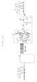
- FIGS. 1A and 1B are the overall configuration diagrams of the ink jet printer according to this embodiment: FIG. 1A is a top plain view of the printer; and FIG. 18 is a front view of the printer.
- a print medium 1 is a line head ink jet printer that is conveyed from the right to the left in the figure in a direction indicated by an arrow in the figure and printed in a printing area on the way of the conveyor.
- ink jet heads according to this embodiment are arranged not only on one place, but also two places.
- Reference numeral 2 in the figure denotes first ink jet heads being provided in the upstream side in the direction to convey the print medium 1.
- Reference numeral 3 denotes second ink jet heads being provided in the downstream side.
- a first conveyor unit 4 is provided below the first ink jet heads 2 for conveying the print medium 1, while a second conveyor unit 5 is provided below the second ink jet heads 3.
- the first conveyor unit 4 comprises four first conveyor belts 6 being spaced apart in a direction crossing the direction to convey the print medium 1 (hereinafter, also referred to as a nozzle array direction).
- the second conveyor unit 5 similarly comprises four second conveyor belts 7 being spaced apart in the direction (nozzles array direction) crossing the direction to convey the print medium 1.
- the four second conveyor belts 7 and the four first conveyor belts 6 are provided alternately.
- This embodiment divides the conveyor belts into two of the first conveyor belts 6 and two of the second conveyor belts 7 at the left side in the nozzle array direction and two of the first conveyor belts 6 and two of the second conveyor belts 7 at the right side in the nozzle array direction. That is, a right drive roller 8R is provided in an overlapping part of the two first conveyor belts 6 and the two second conveyor belts 7 at the right side in the nozzle array direction.
- a left drive roller 8L is provided in an overlapping part of the two first conveyor belts 6 and the two second conveyor belts 7 at the left side in the nozzle array direction.
- a first right driven roller 9R and a first left driven roller 9L are provided at the upstream side, while a second right driven roller low and a second left driven roller 10L are provided at the downstream side.
- the rollers are actually separated at the center part of FIG. 1A , though they are viewed as a series of rollers.
- the two first conveyor belts 6 at the right side in the nozzle array direction are wound around the right drive roller 8R and the first right driven roller 9R.
- the two first conveyor belts 6 at the left side in the nozzle array direction are wound around the left drive roller 8L and the first left driven roller 9L.
- the two second conveyor belts 7 at the right side in the nozzle array direction are wound around the right drive roller 8R and the second right driven roller 10R.
- the two second conveyor belts 7 at the left side in the nozzle array direction are wound around the left drive roller 8L and the second left driven roller 10L.
- the right drive roller 8R connects to the right electric motor 11R, while the left drive roller 8L connect to the left electric motor 11L.
- the first conveyor unit 4 comprising the two first conveyor belts 6 at the right side in the nozzle array direction and the second conveyor unit 5 similarly comprising the two second conveyor belts 7 at the right side in the nozzle array direction synchronize with each other and move at the same speed.
- the first conveyor unit 4 comprising the two first conveyor belts 6 at the left side in the nozzle array direction and the second conveyor unit 5 similarly comprising the two second conveyor belts 7 at the left side in the nozzle array direction synchronize with each other and move at the same speed.
- the right electric motor 11R and the left electric motor 11L rotate at different speeds, conveyor speeds of left and right sides in the nozzle array direction can be changed. Specifically, if the rotation speed of the right electric motor 11R is higher than the rotation speed of the left electric motor 11L, the conveyor speed of the right side in the nozzle array direction can be higher than that of the left side. If the rotation speed of the left electric motor 11L is higher than the rotation speed of the right electric motor 11R, the conveyor speed of the left side in the nozzle array direction can be higher than that of the right side.
- the first ink jet heads 2 and the second ink jet heads 3 are provided to be shifted in the direction to convey the print medium 1 for each of four colors of yellow (Y), magenta (M), cyan (C) and black (K).
- ink is supplied from ink tanks (not shown) for the respective colors via ink supply tubes.
- Each of the ink jet heads 2 and 3 has a plurality of nozzles formed in the direction crossing the direction to convey the print medium 1 (i.e., the nozzle array direction). The nozzles simultaneously jet a necessary amount of ink drops to a necessary position to form and output minute ink dots on the print medium 1.
- a method of jetting and outputting ink from each nozzle of an ink jet head includes an electrostatic scheme, a piezoelectric inkjet, a film-boiling ink jet and the like.
- a drive signal given to an electrostatic gap being an actuator causes a displacement of a vibrating plate in a cavity and a change of pressure in the cavity, in which the change of pressure causes jet and output of ink drops from a nozzle.
- a drive signal given to a piezoelectric element being an actuator causes a displacement of a vibrating plate in a cavity and a change of pressure in the cavity, in which the change of pressure causes jet and output of ink drops from a nozzle.
- a microheater in a cavity is instantaneously heated to 300°C or more to make ink in the film-boiling state and generate bubbles, in which a change of pressure causes jet and output of ink drops from a nozzle.
- Any of the ink output methods can be applied to the present invention.
- the present invention is particularly preferable to a piezoelectric element since the amount of ink drop jet can be modified by modifying the peak value or a degree of voltage increase and decrease of a drive signal.
- the ink drop jetting nozzles of the first ink jet heads 2 are formed only between the four first conveyor belts 6 of the first conveyor unit 4, while the ink drop jetting nozzles of the second ink jet heads 3 are formed only between the four second conveyor belts 7 of the second conveyor unit 5. This is because a cleaning unit described later cleans the respective ink jet heads 2 and 3.
- the first ink jet heads 2 and the second ink jet heads 3 are provided to be shifted from each other in the direction to convey the print medium 1 to cover parts that either of them cannot print.
- a first cleaning cap 12 for cleaning the first ink jet heads 2 is provided under the first ink jet heads 2.
- a second cleaning cap 13 for cleaning the second ink jet heads 3 is provided under the second ink jet heads 3.
- the cleaning caps 12 and 13 are the size to pass between the four first conveyor belts 6 of the first conveyor unit 4 and between the four second conveyor belts 7 of the second conveyor unit 5, respectively.
- the cleaning caps 12 or 13 comprises: a square cap body with a bottom that covers the nozzles formed on the bottom surface of the ink jet heads 2 or 3, i.e., the nozzle side and can be adhered to the nozzle side; an ink absorber provided on the bottom; a tube pump connected to the bottom of the cap body; and an elevator for moving up and down the cap body.
- the elevator moves up the cap body to adhere the body to the nozzle side of the ink jet heads 2 or 3.
- the tube pump makes the cap body under negative pressure in that state, ink drops and bubbles are siphoned off the nozzles being set up on the nozzle side of the ink jet heads 2 or 3 to clean the ink jet heads 2 or 3.
- the cleaning caps 12 and 13 are moved down.
- a pair of gate rollers 14 is provided for modifying timing to feed paper the print medium 1 supplied from a paper feeder 15 and for correcting the skew of the print medium 1, at the upstream side of the first driven rollers 9R and 9L.
- the skew is the torsion of the print medium 1 to the conveyor direction.
- a pickup roller 16 for supplying the print medium 1 is provided above the paper feeder 15.
- Reference numeral 17 in the figure denotes a gate roller motor for driving the gate rollers 14.
- a belt charging unit 19 is provided below the drive rollers 8R and 8L.
- the belt charging unit 19 comprises: a charging roller 20 contacting the first conveyor belts 6 and the second conveyor belts 7 across the drive rollers 8R and 8L; a spring 21 for pressing the charging roller 20 against the first conveyor belts 6 and the second conveyor belts 7; and a power source 18 for imparting electric charge to the charging roller 20.
- the belt charging unit 19 imparts electric charge to the first conveyor belts 6 and the second conveyor belts 7 from the charging roller 20 to charge the belts.
- the belt charging unit 19 when such a type of belt, which incudes a medium or high resistor or insulator, are charged by the belt charging unit 19, electric charge applied on the surface causes induced polarization to the print medium 1 similarly including a high resistor or insulator.
- the print medium 1 can be adsorbed to the belt by electrostatic force that occurs between electric charge generated by the induced polarization and electric charge of the belt surface.
- a charging unit can be a corotron causing electric charge to flood.
- the belt charging unit 19 charges the surfaces of the first conveyor belts 6 and the second conveyor belts 7.
- the gate rollers 14 feed the print medium 1, and a paper pressing roller comprising a spur (not shown) and a roller presses the print medium 1 against the first conveyor belts 6.
- the operation of the induced polarization described above causes the print medium 1 to be adsorbed to the surface of the first conveyor belts 6.
- the electric motors 11R and 11L rotate the drive rollers 8R and 8L, respectively, the rotary drive force is transmitted to the first driven rollers 9R and 9L via the first conveyor belts 6.
- the first conveyor belts 6 are moved downstream in the conveyor direction, the print medium 1 is moved under the first ink jet heads 2, and the nozzles formed on the first ink jet heads 2 jet ink drops for printing.
- the print medium 1 is moved downstream in the conveyor direction toward the second conveyor belts 7 of the second conveyor unit 5.
- the surfaces of the second conveyor belts 7 are also charged by the belt charging unit 19, so that the operation of the induced polarization described above causes the print medium 1 to be adsorbed to the surfaces of the second conveyor belts 7.
- the second conveyor belts 7 are moved downstream in the conveyor direction, the print medium 1 is moved under the second ink jet heads 3, and the nozzles formed on the second ink jet heads jet ink drops for printing.
- a separation unit (not shown) separates the print medium 1 from the surfaces of the second conveyor belts 7 to eject paper toward a paper ejector. If the first and second ink jet heads 2 and 3 need to be cleaned, as described above, the first and second cleaning caps 12 and 13 are moved upward to adhere the cap body to the nozzle side of the first and second ink jet heads 2 and 3. In that state, the cap body made to be under negative pressure to perform cleaning by siphoning off ink drops and bubbles from the nozzles of the first and second ink jet heads 2 and 3. After the cleaning, the first and second cleaning caps 12 and 13 are moved downward.
- the ink jet printer includes a control apparatus for controlling the printer itself.
- the control apparatus processes printing on a print medium by controlling a print unit or a paper feed unit based on print data inputted from a host computer 60 such as a personal computer or a digital camera, as shown in FIG. 2 .
- the control apparatus comprises: an input interface unit 61 for receiving print data inputted from the host computer 60; a control unit 62 comprising a micro computer for executing print processing based on the print data inputted from the input interface unit 61; a gate roller motor driver 63 for controlling drive of the gate roller motor 17; a pickup roller motor driver 64 for controlling drive of a pickup roller motor 51 for driving the pickup roller 16; a head driver 65 for controlling drive of the ink jet heads 2 and 3; a right electric motor driver 66R for controlling drive of the right electric motor 11R; a left electric motor driver 66L for controlling drive of the left electric motor 11L; and an interface 67 for converting an output signal from each of the drivers 63 to 65, 66R and 66L into a control signal used by the external gate roller motor 17, the pickup roller motor 51, the ink jet heads 2 and 3, the right electric motor 11R and the left electric motor 11L and outputting the signal.
- the control unit 62 comprises: a CPU (Central Processing Unit) 62a for executing various processing such as print processing; a RAM (Random Access Memory) 62c for temporally storing print data inputted via the input interface 61 or various data to execute processing to print the print data, or for temporally deploying an application program such as for print processing; and a ROM (Read-Only Memory) 62d comprising a non-volatile semiconductor memory for storing a control program executed by the CPU 62a.
- a CPU Central Processing Unit
- RAM Random Access Memory
- ROM Read-Only Memory
- control unit 62 gets print data (image data) from the host computer 60 via the interface unit 61
- the CPU 62a executes pre-determined processing on the print data, outputs print data (drive signal selection data SI) including which nozzle jets ink drops or how many ink drops are jetted, and outputs a control signal to each of the drivers 63 to 65, 66R and 66L based on the print data and input data from various sensors.
- print data drive signal selection data SI
- the interface unit 67 converts the signal into a drive signal, an actuator corresponding to a plurality of nozzles of an ink jet head, the gate roller motor 17, the pickup roller motor 51, the right electric motor 11R and the left electric motor 111 are actuated to execute paper feed and conveyor of the print medium 1, posture control of the print medium 1, and print processing on the print medium 1.
- the respective components of the control unit 62 are electrically connected to one another via a bus (not shown) .
- the control unit 62 To write waveform forming data DATA to form a drive signal described later into a waveform memory 701 described later, the control unit 62 also outputs a write enable signal DEN, a write clock signal WCLK, and write address data A0 to A3 and writes the 16-bit waveform forming data DATA into the waveform memory 701. Further, the unit 62 outputs the following to the head driver 65: read address data A0 to A3 to read out the waveform forming data DATA stored in the waveform memory 701, a first clock signal ACLK to set timing to latch the waveform forming data DATA being read out from the waveform memory 701, a second clock signal BCLK to set timing to add the latched waveform data, and a clear signal CLER to clear the latch data.
- the head driver 65 comprises a drive waveform generator 70 for forming a drive waveform signal WCOM and an oscillation circuit 71 for outputting a clock signal SCK.
- the drive waveform generator 70 comprises: the waveform memory 701 for storing waveform forming data DATA to generate a drive waveform signal inputted from the control unit 62 in a storage element corresponding to a pre-determined address; a latch circuit 702 for latching the waveform forming data DATA read out from the waveform memory 701 with the first clock signal ACLK described above; an adder 703 for adding output of the latch circuit 702 and the waveform generation data WDATA outputted from a latch circuit 704 described later; the latch circuit 704 for latching addition output of the adder 703 with the second clock signal BCLK described above; and a D/A converter 705 for converting the waveform generation data WDATA outputted from the latch circuit 704 into an analog signal, as shown in FIG. 3 .
- a clear signal CLER outputted from the control unit 62 is inputted to the latch
- the waveform memory 701 includes several bit memory elements being arranged at each designated address stores addresses A0 to A3 and the waveform data DATA, as shown in FIG. 4 .
- the clock signal WCLK and the waveform data DATA are inputted to the addresses A0 to A3 designated by the control unit 62, and input of write enable signal DEN causes the waveform data DATA to be stored in the memory elements.
- write enable signal DEN causes the waveform data DATA to be stored in the memory elements.
- waveform data + ⁇ V1 is written at the address A1
- waveform data - ⁇ V2 is written at the address A2
- waveform data + ⁇ V3 is written at the address A3.
- the clear signal CLER clears data saved by the latch circuits 702 and 704.
- the drive waveform signal WCOM rises to the midpoint potential (offset) according to the waveform data.
- the digital data + ⁇ V1 is saved in the latch circuit 702, as shown in FIG. 5 .
- the saved digital data + ⁇ V1 is inputted to the latch circuit 704 via the adder 703.
- the latch circuit 704 saves output of the adder 703 in synchronization with a rise of the second clock signal BCLK.
- the output of the latch circuit 704 is also inputted to the adder 703. Accordingly, the output of the latch circuit 704, i.e., the drive signal COM is incremented by + ⁇ V1 whenever the second clock signal BCLK rises.
- the waveform data at the address A1 is read in duration T1.
- the signal COM is incremented until the digital data + ⁇ V1 is the triple.
- a drive waveform signal WCOM as shown in FIG. 6 is gained.
- a drive signal output circuit shown in FIG. 7 amplifies the power of the analog signal and supplies the signal as a drive signal COM to the ink jet heads 2 and 3. In this way, actuators such as piezoelectric elements provided for the respective nozzles can be driven, so that the nozzles can jet ink drops.
- the drive signal output circuit comprises: a modulator 24 for modulating a pulse of a drive waveform signal WCOM generated by the drive waveform generator 70; a digital power amplifier 25 for amplifying power of the modulated (PWM) signal subjected to the pulse modulation by the modulator 24; and a low pass filter 26 for smoothing the modulated (PWM) signal subjected to the power amplification by the digital power amplifier 25.
- a time of a rise of the drive signal COM is a stage to increase the volume of a cavity (pressure chamber) communicating with a nozzle and to pull in ink (pull in meniscus, from the viewpoint of the ink-jetted surface).
- a time of a fall of the drive signal COM is a stage to decrease the volume of the cavity and to push out ink (push out meniscus, from the viewpoint of the ink-jetted surface). As a result of the pushing-cut of ink, the nozzle jets ink drops.
- a waveform of the drive signal COM or the drive waveform signal WCOM can be modified with waveform data 0, + ⁇ V1, - ⁇ V2, + ⁇ V3, the first clock signal ACLK and the second clock signal BCLK written at the addresses A0 to A3, as easily inferred from the above description.
- a voltage increase and decrease degree and the peak value of the drive signal COM in a voltage trapezoid wave are variously changed so that the amount of pulled in ink, the pull-in speed, the amount of pushed out ink and the push-out speed can be changed. This can change the amount of jet of ink drops to gain different sizes of ink dots.
- a single drive signal CCM is selected from the signals to be supplied to a piezoelectric actuator 22 for jet of ink drops; or a plurality of drive signals COM are selected to be supplied to the piezoelectric actuator 22 for jet of ink drops for times, thereby gaining various sizes of ink dots.
- a drive pulse at the far left in FIG. 6 only pulls in ink but does not pull out ink. This is called fine vibration, which is used to inhibit or prevent a nozzle from being dried without jetting ink drops.
- the following are inputted to the ink jet heads 2 and 3: the drive signal COM generated by the drive signal output circuit; a drive signal selection data signal SI to select a nozzle for jet based on print data and to decide time of connection to the drive signal COM of an actuator such as a piezoelectric element; a latch signal LAT and a channel signal CH to connect the drive signal COM and the actuators of the ink jet heads 2 and 3 based on the drive signal selection data SI after nozzle selection data is inputted to all nozzles; and a clock signal SCK to transmit the drive signal selection data signal SI as a serial signal to the ink jet heads 2 and 3.
- the drive signal COM generated by the drive signal output circuit
- a drive signal selection data signal SI to select a nozzle for jet based on print data and to decide time of connection to the drive signal COM of an actuator such as a piezoelectric element
- a latch signal LAT and a channel signal CH to connect the drive signal COM and the actuators of the ink jet heads 2 and 3
- FIG. 8 is a block diagram of a selector for connecting the drive signal COM to the actuator such as a piezoelectric element.
- the selector comprises: a shift register 211 for saving drive signal selection data SI to designate an actuator such as a piezoelectric element corresponding to a nozzle for jetting ink drops; a latch circuit 212 for temporally saving data of the shift register 211; a level shifter 213 for converting a level of output of the latch circuit 212; and a selection switch 201 for connecting a drive signal COM to an actuator such as a piezoelectric element depending on output of the level shifter.
- a storage area of the register serially shifts from the first part to latter parts depending on an inputted pulse of a clock signal SICK.
- the latch circuit 212 latches each output signal of the shift register 211 according to an inputted latch signal LAT.
- the level of a signal saved in the latch circuit 212 is converted into a voltage level to turn on/off the selection switch 201 in the next part by the level shifter 213. This is because voltage of the drive signal COM is higher than output voltage of the latch circuit 212, and a range of the operating voltage of the selection switch 201 is also set to a high range accordingly.
- the actuator such as a piezoelectric element of which selection switch 201 is closed by the level shifter 213 is connected to the drive signal COM at a time for connection of the drive signal selection data SI.
- a drive signal selection data signal SI of the shift register 211 is saved in the latch circuit 212
- the next print information is inputted to the shift register 211, and data saved in the latch circuit 212 is serially updated each time ink drops are jetted.
- Reference character HGND in the figure denotes a ground terminal of the actuator such as a piezoelectric element.
- the selection switch 201 also maintains input voltage of the actuator 22 at voltage immediately before separation even after the actuator such as a piezoelectric element is separated from a drive signal COM.
- FIG. 9 shows specific configuration between the modulator 24 of the drive signal output circuit and the low pass filter 26 described above.
- a general pulse width modulator (PWM) is used for the modulator 24 for modulating a pulse of a drive waveform signal WCOM.
- the modulator 24 comprises a known triangular wave oscillator 32, and a comparator 31 for comparing a triangular wave outputted from the triangular wave oscillator 32 and the drive waveform signal WCOM.
- the modulator 24 outputs a modulated (PWM) signal Hi if the drive waveform signal WCOM is a triangular wave or above, and outputs a modulated (PWM) signal Lo if the drive waveform signal WCOM is below a triangular wave, as shown in FIG. 10 .
- This embodiment employs a pulse width modulator as a pulse modulator; instead, a pulse density modulator (PDM) can be employed.
- PDM pulse density modulator
- the digital power amplifier 25 comprises a half bridge driver stage 33 including both a MOSFETTrP and a MOSFETTrN to actually amplify power, and a gate drive circuit 34 for modifying the gate-source signals GP and GN of the MOSFETTrP and TrN based on a modulated (PWM) signal from the modulator 24.
- the half bridge driver stage 33 is push-pull combination of the high-side MOSFETTrP and the low-side MOSFETTrN. Label a gate-source signal of the high-side MOSFETTrP as GP, a gate-source signal of the low-side MOSFETPrN as GN, and output of the half bridge driver stage 33 as Va.
- a voltage value Vgs of the gate-source signals GP and GN of the respective MOSFETTrP and TrN is an enough voltage value to turn ON the MOSFETTrP and TrN.
- the output Va from the half bridge driver stage 33 of the digital power amplifier 25 is supplied as a drive signal COM to the selection switch 201 via the low pass filter 26.
- the low pass filter 26 is a low-pass filter including combination of two coils L1 and L2 and two capacitors C1 and C2.
- the low pass filter 26 being a low-pass filter is designed to sufficiently attenuate a high-frequency component, i.e., a power-amplified modulated (PWM) signal component of the output Va from the half bridge driver stage 33 of the digital power amplifier 25 and not to attenuate a drive signal component COM (or drive waveform component WCOM).
- PWM power-amplified modulated
- the MOSFETs operate as switch elements so that currents flow into the MOSFETs in the ON state.
- a drain-source resistance value is very small, hence the power loss hardly generates.
- the power loss of the digital power amplifier 25 is significantly small so that small MOSFETs can be used, dispensing with a cooling unit such as a cooling plate radiator.
- the efficiency is about 30% to linearly drive a transistor, while the efficiency of a digital power amplifier is 90% or more.
- a cooling plate radiator of a transistor should be of a size of a 60-mm square for a single transistor. Dispensing with such a cooling plate radiator is overwhelmingly advantageous in actual layout.
- the drive waveform generator 70 generates a drive waveform signal WCOM being standard of a signal to control drive of an actuator such as a piezoelectric element
- the modulator 24 such as a pulse width modulator modulates a pulse of the generated drive waveform signal WCOM
- the digital power amplifier 25 amplifies the power of the modulated signal subjected to the pulse modulation
- the low pass filter 26 smoothes the powder-amplified modulated signal subjected to the power amplification and supplies the signal as a drive signal to the actuator.
- filter characteristics of the low pass filter 26 are set to sufficiently smooth only a power-amplified modulated signal component so that rapid rise and fall of a drive signal to the actuators are enabled and the digital power amplifier 25 with efficient power amplification can efficiently amplify the power of a drive signal.
- This dispenses with a cooling unit such as a cooling plate radiator.
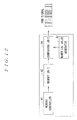
- FIG. 12 shows another embodiment of the drive waveform generator and the modulator of the head drive apparatus of an ink jet printer according to the present invention.
- the D/A converter 705 converts drive waveform signals subjected to digital composition into analog signals and outputs the result.
- a memory controller 41 reads out digital waveform data from a memory unit 42
- a comparing unit 44 compares the read out digital waveform data with a numerical value from a numerical value generator 43 corresponding to a triangular wave to decide whether a modulated (PWM) signal is Hi or Lo, and outputs the result as a modulated (PWM) signal.
- PWM modulated
- the memory controller 41, the memory unit 42, the numerical value generator 43 and the comparing unit 44 can be embedded in a CPU or a gate array.
- the memory controller 41 and the memory unit 42 correspond to the drive waveform signal generation unit of the present invention, and the numerical value generator 43 and the comparing unit 44 constitute the modulator.
- FIG. 14 shows overall configuration of a drive signal output circuit employing a triangular wave comparison pulse width modulator 41 as the modulator 24.
- the triangular wave comparison pulse width modulator 41 comprises the known triangular wave oscillator 32, and the comparator 31 for comparing a triangular wave outputted from the triangular wave oscillator 32 with the drive waveform signal WCOM.
- the triangular wave comparison pulse width modulator 41 outputs a modulated (PWM) signals Hi if the drive waveform signal WCOM is a triangular wave or above, and outputs a modulated (PWM) signal Lo if the drive waveform signal WCOM is below a triangular wave, as described above.
- PWM modulated
- Modulated signals from the triangular wave comparison pulse width modulator 41 are referred to as IH and IL.
- IH and IL are complete rectangular waves (pulses)
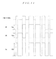
- output signals of a gate driver 34 i.e., gate signals GP and GN of the MOSFETTrP and TrN rise during a short time Tr and fall during a short time Tf so that the signals change to trapezoid waves.
- the gate signals GP and GN are in opposite directions (i.e., reversed) at a time so that the two gate signals GP and GN sometimes overlap with each other.
- the MOSFETTrP and TrN of the half bridge driver stage 33 When the gate signals GP and GN overlap with each other, the MOSFETTrP and TrN of the half bridge driver stage 33 simultaneously turn to the ON state and a short-through current flows into them, causing power loss.
- the power loss is referred to as transition loss or switching loss. The power loss occurs whenever the MOSFETTrP and TrN turn ON/OFF so that it is larger as a frequency is higher.
- a dead time Td can be set for the modulated signals IH and IL to be inputted to the gate driver 34 at different times so that the gate signals GP and GN from the gate driver 34 do not actually overlap with each other.
- a drive waveform signal level and pulse duty should be originally linear.
- pulse duty is not linear in an area of a low or high drive waveform signal level as shown by a solid line in FIG. 17 , causing distortion of a drive signal COM shown by a solid line in FIG. 18 .
- a self-oscillating pulse width modulator PWM
- the circuit has an advantage of generating a power-amplified modulated signal of the half bridge driver stage 33.
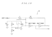
- FIG. 19 shows one example of a self-oscillating pulse width modulator 42.
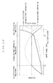
- FIG. 20 shows output characteristics of the self-oscillating pulse width modulator 42.
- the seif-oscillating pulse width modulator 42 when a level of an input signal, or a drive waveform signal WCOM in this case is low, the frequency of a triangular wave is low.
- the pulse width of a modulated signal can be large in an area of a low input signal level of the input signal, i.e., drive waveform signal WCOM. This can cause generation of a power-amplified modulated signal of the half bridge driver stage 33.
- the frequency of a triangular wave is large and the operation frequency of the switching transistor is also large at the median of input signal levels of an input signal, or a drive waveform signal WCOM in this case, i.e., around duty ratio 50%, increasing switching loss as described above.
- a frequency band of a high frequency component of output Va is wide so that it is difficult to design a low pass filter in a latter part.
- the triangular wave comparison pulse width modulator 41 and the self-oscillating pulse width modulator 42 are arranged to be together in the modulator 24, as shown in FIG. 21 .
- a drive waveform signal WCOM is inputted to one of the pulse width modulators selected by a modulation method selection circuit 43. Output from the modulator is labeled as a modulated signal IH, while an output being further reversed by an inverter 44 is labeled as a modulated signal IL.
- the modulation method selection circuit 43 selects a pulse width modulator by referring to the drive waveform signal WCOM itself.
- PWM triangular wave comparison pulse width modulation
- VL low voltage pre-determined value
- VH high voltage pre-determined value
- PWM self-oscillating pulse width modulation
- the drive waveform generator 70 generates a drive waveform signal WCOM being standard of a signal to control drive of an actuator such as a piezoelectric element
- the modulator 24 such as a pulse width modulator modulates a pulse of the generated drive waveform signal WCOM
- the digital power amplifier 25 amplifies the power of the modulated signal subjected to the pulse modulation
- the low pass filter 26 smoothes the power-amplified modulated signal subjected to the power amplification and supplies the signal as a drive signal to the actuator.
- filter characteristics of the low pass filter 26 are set to sufficiently smooth only a high frequency component of a power-amplified modulated signal so that a correct drive signal can be generated to the actuators and the digital power amplifier 25 with efficient power amplification can efficiently amplify the power of a drive signal.
- This dispenses with a cooling unit such as a cooling plate radiator.
- a pulse modulation method can be changed depending on an input signal level of a drive waveform signal.
- a triangular wave comparison pulse width modulation method is used. This can inhibit or prevent distortion of an output signal and power loss.
- FIG. 23 shows another example of the modulator 24 as another embodiment of the head drive apparatus of an ink jet printer according to the present invention.
- a first pulse width modulator 45 and a second pulse width modulator 46 employing different pulse width modulation methods are arranged to be adjacent to each other in the modulator 24.
- a drive waveform signal WCOM is inputted to one of the pulse width modulators selected by a modulation method selection circuit 43. Output from the modulator is labeled as a modulated signal IH, while an output being further reversed by an inverter 44 is labeled as a modulated signal IL.
- the modulation method selection circuit 43 is configured to select the first pulse width modulator 45 or the second pulse width modulator 46 depending on each control signal.
- a pulse width modulation method to be selected is not limited to the triangular wave comparative or self-oscillating described above. A method of selecting a pulse width modulation method can also depend on each control signal.
- the head drive apparatus of an ink jet printer according to the present invention can be applied to all types of ink jet printers including a multipass printer.
Landscapes
- Engineering & Computer Science (AREA)
- Microelectronics & Electronic Packaging (AREA)
- Power Engineering (AREA)
- Particle Formation And Scattering Control In Inkjet Printers (AREA)
Abstract
Description
- The present invention relates to an ink jet printer in which a plurality of nozzles jet minute ink drops of liquid ink of a plurality of colors and particles of ink (ink dots) are formed on a print medium to draw pre-determined characters and images.
- An ink jet printer as in the above generally accomplishes low-cost and high-quality color printed material easily. As such, it is widely used not only in offices but also by general users along with popularization of a personal computer and a digital camera.
Generally, in such an ink jet printer, a moving part called a carriage, for example, integrally comprising ink cartridges and print heads moves back and forth on a print medium in a direction crossing a direction to convey the medium and nozzles of the print head jet (eject) liquid ink drops to form minute ink dots on the print medium. In this manner, pre-determined characters or images are drawn on the print medium to create desired printed material. The carriage comprises ink cartridges for four colors including black (and yellow, magenta, cyan) and a print head for each of the colors, so that not only monochrome print but also full color print in combination of the respective colors can be easily performed (further, print in six colors including the colors, light cyan and light magenta, seven colors, and eight colors are practically implemented). - The above type of ink jet printer for executing print by moving the ink jet heads on the carriage back and forth in a direction crossing a direction to convey a print medium in the above manner, the ink jet heads must be moved back and forth for about ten times or for more than tens of times to neatly print a whole page. Therefore, it has a drawback in that it takes a longer time for printing than a print apparatus in another scheme, for example, a laser printer or a copying machine using electrographic technique.
On the other hand, in an ink jet printer comprising ink jet heads (do not need to be integrated) of the same length as the width of a print medium but not comprising a carriage, the ink jet heads do not need to be moved in a width direction of the print medium so that one-pass printing is possible, enabling quick printing similar to a laser printer. An ink jet printer in the former scheme is generally called a "multi-pass (serial) ink jet printer", while an ink jet printer in the latter scheme is generally called a "line head ink jet printer". - The above types of ink jet printers are required to provide further higher gradation. Gradation is the density of each color included in a pixel represented by an ink dot: the size of an ink dot depending on the density of a color of each pixel is called gradient, while the number of gradients represented by an ink dot is called the number of gradations. High gradation means that the number of gradations is large. To change gradient, it is necessary to change a drive pulse to an actuator provided for an ink jet head. For example, if an actuator is a piezoelectric element, when a voltage value applied to the piezoelectric element is large, the magnitude of displacement (distortion) of the piezoelectric element (precisely, a vibrating plate) is also large. This is used to change the gradient of an ink dot.
- According to
JP-A-10-81013 - A method of generating a drive signal (or drive pulse) is illustrated in
FIG. 2 ofJP-A-2004-306434 FIG. 3 of the document, in which a linear drive amplifies a drive signal. However, in a current amplifier with such configuration, a linear drive itself of a transistor is inefficient. Moreover, such an amplifier has a drawback of a large circuit size since the transistor itself should be large for a countermeasure against heat, or the transistor needs a cooling plate radiator. Particularly, the largeness of the cooling plate radiator is a major obstacle to the layout. - To resolve the drawback,
JP-A-2005-35062 - However, a DC/DC converter is originally designed to generate a constant voltage. As such, the head drive apparatus of an ink jet printer using the DC/DC converter in
JP-A-2005-35062 JP-A-2004-306434 - An object of the present invention is to provide a head drive apparatus of an ink jet printer that enables rapid rise and fall of a drive signal to an actuator, does not require a cooling unit such as a cooling plate radiator, and can inhibit or prevent distortion of a drive signal or power loss.
[First Aspect] To solve the above problems, a head drive apparatus of an ink jet printer according to a first aspect characterized by including: a plurality of nozzles for jetting liquid drops that are provided for an ink jet head; actuator provided in correspondence to the nozzles; and a drive unit that applies a drive signal to the actuators, wherein the drive unit comprises: a drive waveform generator that generates a drive waveform signal being standard of a signal to control drive of the actuators; a modulator that modulates a pulse of a drive waveform signal generated by the drive waveform generator; a digital power amplifier for amplifying power of a modulated signal subjected to the pulse modulation by the modulator; and a low pass filter for smoothing a power-amplified modulated signal subjected to the power amplification by the digital power amplifier and supplying the signal as a drive signal to the actuators. - In the head drive apparatus of an ink jet printer according to the first aspect, the drive waveform generator generates a drive waveform signal being standard of a signal to control drive of the actuators, the modulator modulates a pulse of the generated drive waveform signal, the digital power amplifier amplifies the power of the modulated signal subjected to the pulse modulation, the low pass filter smoothes the power-amplified modulated signal subjected to the power amplification and supplies the signal as a drive signal to the actuator. Thus, filter characteristics of the low pass filter are set to sufficiently smooth only a power-amplified modulated signal component so that rapid rise and fall of a drive signal to the actuators are enabled and the digital power amplifier with efficient power amplification can efficiently amplify the power of a drive signal. This dispenses with a cooling unit such as a cooling plate radiator.
- [Second Aspect] A head drive apparatus of an ink jet printer according to a second aspect characterized by including: a plurality of nozzles for jetting liquid drops that are provided for an ink jet head; actuators provided in correspondence to the nozzles; and a drive unit that applies a drive signal to the actuators, wherein the drive unit comprises: a drive waveform generator that generates a drive waveform signal being standard of a signal to control drive of the actuators; a modulator that modulates a pulse of a drive waveform signal generated by the drive waveform generator; a digital power amplifier for amplifying power of a modulated signal subjected to the pulse modulation by the modulator; and a low pass filter for smoothing a power-amplified modulated signal subjected to the power amplification by the digital power amplifier and supplying the signal as a drive signal to the actuators, and the modulator comprises a pulse modulation method changing unit that changes a pulse modulation method depending on an input signal level of a drive waveform signal.
- The purse modulation method includes well known triangular wave comparison pulse width modulation to compare an analog signal and a standard triangular wave and decide Hi/Lo. The triangular wave comparison pulse width modulation can gain a modulated signal with a pulse duty in proportion to an input signal. However, simultaneous and opposite ON/OFF control of two switching transistors of a digital power amplifier by using a modulated signal produced by the triangular wave comparison pulse width modulation causes large power loss. However, if ON/OFF control of the switching transistors at different times, a power-amplified modulated signal is not generated in a low ON-duty area (= high OFF-duty) or a low OFF-duty (= high ON-duty) area, causing distortion of a drive signal. Meanwhile, self-oscillating pulse width modulation has an advantage in that a power-amplified modulated signal can be generated in a low ON-duty area or a low OFF-duty area. However, there is a trade-off that when the duty ratio is closer to 50%, the pulse frequency is higher and switching loss increases.
- In the head drive apparatus of an ink jet printer according to the second aspect, the drive waveform generator generates a drive waveform signal being standard of a signal to control drive of the actuators, the modulator modulates a pulse of the generated drive waveform signal, the digital power amplifier amplifies the power of the modulated signal subjected to the pulse modulation, the low pass filter smoothes the power-amplified modulated signal subjected to the power amplification and supplies the signal as a drive signal to the actuator. Thus, filter characteristics of the low pass filter are set to sufficiently smooth only a high frequency component of a power-amplified modulated signal so that a correct drive signal can be generated to the actuators and the digital power amplifier with efficient power amplification can efficiently amplify the power of a drive signal. This dispenses with a cooling unit such as a cooling plate radiator.
- A pulse modulation method can be changed depending on an input signal level of a drive waveform signal. Thus, a self-oscillating pulse width modulation method is used in a low ON-duty (= high OFF-duty) area, that is an area with a low input signal level of a drive waveform signal, and a low OFF-duty (= high ON-duty) area, that is an area with a high input signal level of a drive waveform signal. In the other areas, a triangular wave comparison pulse width modulation method is used. This can inhibit or prevent distortion of a drive signal and power loss.
- [Third Aspect] A head drive apparatus of an ink jet printer according to a third aspect is characterized in that in the head drive apparatus of an ink jet printer according to the second aspect, the pulse modulation method changing unit uses the triangular wave comparison pulse width modulation method for pulse modulation if the input signal level of the drive waveform signal is in a preset range, and uses the self-oscillating pulse width modulation method for pulse modulation if the input signal level of the drive waveform signal is lower than the preset range.
- In the head drive apparatus of an ink jet printer according to the third aspect, if an input signal level of a drive waveform signal is in a preset range, the triangular wave comparison pulse width modulation method is used for pulse modulation, and if an input signal level of a drive waveform signal is lower than the preset range, the self-oscillating pulse width modulation method is used for pulse modulation. This can effectively inhibit or prevent distortion of a drive signal or power loss.
[Fourth Aspect] A head drive apparatus of an ink jet printer according to a fourth aspect is characterized in that in the head drive apparatus of an ink jet printer according to the second or third aspect, the pulse modulation method changing unit uses the triangular wave comparison pulse width modulation method for pulse modulation if the input signal level of the drive waveform signal is in a preset range, and uses the self-oscillating pulse width modulation method for pulse modulation if the input signal level of the drive waveform signal is higher than the preset range. - In the head drive apparatus of an ink jet printer according to the fourth aspect, if an input signal level of a drive waveform signal is in a preset range, the triangular wave comparison pulse width modulation method is used for pulse modulation, and if an input signal level of a drive waveform signal is higher than the preset range, the self-oscillating pulse width modulation method is used for pulse modulation. This can effectively inhibit or prevent distortion of a drive signal or power loss.
[Fifth Aspect] A head drive control method for an ink jet printer according to a fifth aspect is characterized by controlling drive of the actuator by: a drive waveform signal generation step of generating a drive waveform signal being standard of a signal to control drive of actuators provided in correspondence to a plurality of nozzles for jetting liquid drops provided for the ink jet head; a modulation step of modulating a pulse of the drive waveform signal generated at the drive waveform signal generation step; a step of amplifying power of a modulated signal subjected to the pulse modulation at the modulation step by a digital power amplifier; and a step of smoothing a power-amplified modulated signal subjected to the power amplification by the digital power amplifier and supplying the signal as a drive signal to the actuator. - With the head drive control method for an ink jet printer according to the fifth aspect, rapid rise and fall of a drive signal to the actuators are enabled and the power of a drive signal can be efficiently amplified so that it is no longer necessary to cool a cooling plate radiator and the like, similarly to the first aspect. [Sixth Aspect] A head drive control method for an ink jet printer according to a sixth aspect is characterized in that the modulation step includes using the triangular wave comparison pulse width modulation method for pulse modulation if the input signal level of the drive waveform signal is in a preset range, and using the self-oscillating pulse width modulation method for pulse modulation if the input signal level of the drive waveform signal is lower or higher than the preset range.
- Witch the head drive control method for an ink jet printer according to the sixth aspect, distortion of a drive signal or power loss can be effectively inhibited or prevented similarly the second to fourth aspects. [Seventh Aspect] An ink jet printer according to a seventh aspect comprises the head drive apparatus according to any of the first to fourth aspects.
-
-
FIGS. 1A and 1B are the overall configuration diagrams showing a first embodiment of a line head ink jet printer to which a head drive apparatus of the ink jet printer according to the present invention is applied: (a) is a top plain view and (b) is a front view; -
FIG. 2 is a block diagram of a control apparatus of the ink jet printer inFIGS. 1A and 1B ; -
FIG. 3 is a block diagram of a drive waveform generator inFIG. 2 ; -
FIG. 4 is a diagram illustrating a waveform memory inFIG. 3 ; -
FIG. 5 is a diagram illustrating drive waveform signal generation; -
FIG. 6 is a diagram illustrating a drive waveform signal or a drive signal joined time-sequentially; -
FIG. 7 is a block diagram of a drive signal output circuit; -
FIG. 8 is a block diagram of a selector for connecting a drive signal to an actuator; -
FIG. 9 is a block diagram showing details of a modulator, a digital power amplifier and a low pass filter of the drive signal output circuit inFIG. 7 ; -
FIG. 10 is a diagram illustrating the operation of the modulator inFIG. 9 ; -
FIG. 11 is a diagram illustrating the operation of the digital power amplifier inFIG. 9 ; -
FIG. 12 shows another embodiment of the head drive apparatus of an ink jet printer according to the present invention, and is a block diagram of a drive waveform generator and a modulator; -
FIG. 13 shows a second embodiment of the line head ink jet printer to which the head drive apparatus of an ink jet printer according to the present invention is applied, and is a block diagram showing details of a modulator, a digital power amplifier and a low pass filter of a drive signal output circuit; -
FIG. 14 is an overall configuration diagram of a drive signal output circuit using a triangular wave comparison pulse width modulator; -
FIG. 15 is a diagram illustrating a MOSFET gate signal in a digital power amplifier with the triangular wave comparison pulse width modulator; -
FIG. 16 is a diagram illustrating a MOSFET gate signal and an output signal in the digital power amplifier if dead time is set; -
FIG. 17 is a diagram illustrating the relation between an input signal level and pulse duty according to the gate signal inFIG. 16 ; -
FIG. 18 is a diagram illustrating distortion of a drive signals according to the pulse duty inFIG. 17 ; -
FIG. 19 is a diagram illustrating one example of a self-oscillating pulse width modulator; -
FIG. 20 is a diagram illustrating frequency and pulse width characteristics in self-oscillating pulse width modulation; -
FIG. 21 is a block diagram of the modulator inFIG. 13 ; -
FIG. 22 is a diagram illustrating frequency and pulse width characteristics in the pulse width modulation inFIG. 21 ; and -
FIG. 23 is a block diagram of a modulator showing another embodiment of the head drive apparatus of an ink jet printer according to the present invention. - 1: print medium; 2: first ink jet head; 3: second ink jet head; 4: first conveyor unit; 5: second conveyor unit; 6: first conveyor belt; 7: second conveyor belt; 8R, 8L: drive rollers; 9R, 9L: first driven rollers; 10R, 10L: second driven rollers; 11R, 11L: electric motors; 24: modulator; 25: digital power amplifier; 26: low pass filter; 31: comparator; 32: triangular wave oscillator; 33: half bridge driver stage; 34: gate drive circuit; 41: memory controller; 42: memory unit; 43: numerical value generator; 44: comparing unit; 70: drive waveform generator
- A first embodiment of an ink jet printer according to the present invention will be described with reference to the drawings.
FIGS. 1A and 1B are the overall configuration diagrams of the ink jet printer according to this embodiment:FIG. 1A is a top plain view of the printer; andFIG. 18 is a front view of the printer. InFIGS. 1A and 1B , aprint medium 1 is a line head ink jet printer that is conveyed from the right to the left in the figure in a direction indicated by an arrow in the figure and printed in a printing area on the way of the conveyor. However, ink jet heads according to this embodiment are arranged not only on one place, but also two places. -
Reference numeral 2 in the figure denotes first ink jet heads being provided in the upstream side in the direction to convey theprint medium 1.Reference numeral 3 denotes second ink jet heads being provided in the downstream side. Afirst conveyor unit 4 is provided below the first ink jet heads 2 for conveying theprint medium 1, while asecond conveyor unit 5 is provided below the second ink jet heads 3. Thefirst conveyor unit 4 comprises fourfirst conveyor belts 6 being spaced apart in a direction crossing the direction to convey the print medium 1 (hereinafter, also referred to as a nozzle array direction). Thesecond conveyor unit 5 similarly comprises foursecond conveyor belts 7 being spaced apart in the direction (nozzles array direction) crossing the direction to convey theprint medium 1. - The four
second conveyor belts 7 and the fourfirst conveyor belts 6 are provided alternately. This embodiment divides the conveyor belts into two of thefirst conveyor belts 6 and two of thesecond conveyor belts 7 at the left side in the nozzle array direction and two of thefirst conveyor belts 6 and two of thesecond conveyor belts 7 at the right side in the nozzle array direction. That is, aright drive roller 8R is provided in an overlapping part of the twofirst conveyor belts 6 and the twosecond conveyor belts 7 at the right side in the nozzle array direction. Aleft drive roller 8L is provided in an overlapping part of the twofirst conveyor belts 6 and the twosecond conveyor belts 7 at the left side in the nozzle array direction. A first right drivenroller 9R and a first left drivenroller 9L are provided at the upstream side, while a second right driven roller low and a second left drivenroller 10L are provided at the downstream side. The rollers are actually separated at the center part ofFIG. 1A , though they are viewed as a series of rollers. The twofirst conveyor belts 6 at the right side in the nozzle array direction are wound around theright drive roller 8R and the first right drivenroller 9R. The twofirst conveyor belts 6 at the left side in the nozzle array direction are wound around theleft drive roller 8L and the first left drivenroller 9L. The twosecond conveyor belts 7 at the right side in the nozzle array direction are wound around theright drive roller 8R and the second right drivenroller 10R. The twosecond conveyor belts 7 at the left side in the nozzle array direction are wound around theleft drive roller 8L and the second left drivenroller 10L. Theright drive roller 8R connects to the rightelectric motor 11R, while theleft drive roller 8L connect to the leftelectric motor 11L. As such, when the rightelectric motor 11R rotates theright drive roller 8R, thefirst conveyor unit 4 comprising the twofirst conveyor belts 6 at the right side in the nozzle array direction and thesecond conveyor unit 5 similarly comprising the twosecond conveyor belts 7 at the right side in the nozzle array direction synchronize with each other and move at the same speed. When the leftelectric motor 11L rotates theleft drive roller 8L, thefirst conveyor unit 4 comprising the twofirst conveyor belts 6 at the left side in the nozzle array direction and thesecond conveyor unit 5 similarly comprising the twosecond conveyor belts 7 at the left side in the nozzle array direction synchronize with each other and move at the same speed. However, if the rightelectric motor 11R and the leftelectric motor 11L rotate at different speeds, conveyor speeds of left and right sides in the nozzle array direction can be changed. Specifically, if the rotation speed of the rightelectric motor 11R is higher than the rotation speed of the leftelectric motor 11L, the conveyor speed of the right side in the nozzle array direction can be higher than that of the left side. If the rotation speed of the leftelectric motor 11L is higher than the rotation speed of the rightelectric motor 11R, the conveyor speed of the left side in the nozzle array direction can be higher than that of the right side. - The first ink jet heads 2 and the second ink jet heads 3 are provided to be shifted in the direction to convey the
print medium 1 for each of four colors of yellow (Y), magenta (M), cyan (C) and black (K). To the respective ink jet heads 2 and 3, ink is supplied from ink tanks (not shown) for the respective colors via ink supply tubes. Each of the ink jet heads 2 and 3 has a plurality of nozzles formed in the direction crossing the direction to convey the print medium 1 (i.e., the nozzle array direction). The nozzles simultaneously jet a necessary amount of ink drops to a necessary position to form and output minute ink dots on theprint medium 1. This is performed for each color so that one-pass printing can be performed by causing theprint medium 1 conveyed by thefirst conveyor unit 4 and thesecond conveyor unit 5 to pass through the heads only once. That is, the areas where the ink jet heads 2 and 3 are arranged correspond to printing areas. - A method of jetting and outputting ink from each nozzle of an ink jet head includes an electrostatic scheme, a piezoelectric inkjet, a film-boiling ink jet and the like. In the electrostatic scheme, a drive signal given to an electrostatic gap being an actuator causes a displacement of a vibrating plate in a cavity and a change of pressure in the cavity, in which the change of pressure causes jet and output of ink drops from a nozzle. In the piezoelectric inkjet, a drive signal given to a piezoelectric element being an actuator causes a displacement of a vibrating plate in a cavity and a change of pressure in the cavity, in which the change of pressure causes jet and output of ink drops from a nozzle. In the film-boiling ink jet, a microheater in a cavity is instantaneously heated to 300°C or more to make ink in the film-boiling state and generate bubbles, in which a change of pressure causes jet and output of ink drops from a nozzle. Any of the ink output methods can be applied to the present invention. Along them, the present invention is particularly preferable to a piezoelectric element since the amount of ink drop jet can be modified by modifying the peak value or a degree of voltage increase and decrease of a drive signal.
- The ink drop jetting nozzles of the first ink jet heads 2 are formed only between the four
first conveyor belts 6 of thefirst conveyor unit 4, while the ink drop jetting nozzles of the second ink jet heads 3 are formed only between the foursecond conveyor belts 7 of thesecond conveyor unit 5. This is because a cleaning unit described later cleans the respective ink jet heads 2 and 3. However, one-pass full-page printing cannot be accomplished only by either of the ink jet heads. Accordingly, the first ink jet heads 2 and the second ink jet heads 3 are provided to be shifted from each other in the direction to convey theprint medium 1 to cover parts that either of them cannot print. - A
first cleaning cap 12 for cleaning the first ink jet heads 2 is provided under the first ink jet heads 2. Asecond cleaning cap 13 for cleaning the second ink jet heads 3 is provided under the second ink jet heads 3. The cleaning caps 12 and 13 are the size to pass between the fourfirst conveyor belts 6 of thefirst conveyor unit 4 and between the foursecond conveyor belts 7 of thesecond conveyor unit 5, respectively. The cleaning caps 12 or 13 comprises: a square cap body with a bottom that covers the nozzles formed on the bottom surface of the ink jet heads 2 or 3, i.e., the nozzle side and can be adhered to the nozzle side; an ink absorber provided on the bottom; a tube pump connected to the bottom of the cap body; and an elevator for moving up and down the cap body. As such, the elevator moves up the cap body to adhere the body to the nozzle side of the ink jet heads 2 or 3. When the tube pump makes the cap body under negative pressure in that state, ink drops and bubbles are siphoned off the nozzles being set up on the nozzle side of the ink jet heads 2 or 3 to clean the ink jet heads 2 or 3. When the cleaning finishes, the cleaning caps 12 and 13 are moved down. - A pair of
gate rollers 14 is provided for modifying timing to feed paper theprint medium 1 supplied from apaper feeder 15 and for correcting the skew of theprint medium 1, at the upstream side of the first drivenrollers print medium 1 to the conveyor direction. Apickup roller 16 for supplying theprint medium 1 is provided above thepaper feeder 15.Reference numeral 17 in the figure denotes a gate roller motor for driving thegate rollers 14. - A
belt charging unit 19 is provided below thedrive rollers belt charging unit 19 comprises: a chargingroller 20 contacting thefirst conveyor belts 6 and thesecond conveyor belts 7 across thedrive rollers spring 21 for pressing the chargingroller 20 against thefirst conveyor belts 6 and thesecond conveyor belts 7; and a power source 18 for imparting electric charge to the chargingroller 20. Thebelt charging unit 19 imparts electric charge to thefirst conveyor belts 6 and thesecond conveyor belts 7 from the chargingroller 20 to charge the belts. Generally, when such a type of belt, which incudes a medium or high resistor or insulator, are charged by thebelt charging unit 19, electric charge applied on the surface causes induced polarization to theprint medium 1 similarly including a high resistor or insulator. Theprint medium 1 can be adsorbed to the belt by electrostatic force that occurs between electric charge generated by the induced polarization and electric charge of the belt surface. A charging unit can be a corotron causing electric charge to flood. - In the ink jet printer, the
belt charging unit 19 charges the surfaces of thefirst conveyor belts 6 and thesecond conveyor belts 7. In that state, thegate rollers 14 feed theprint medium 1, and a paper pressing roller comprising a spur (not shown) and a roller presses theprint medium 1 against thefirst conveyor belts 6. Then, the operation of the induced polarization described above causes theprint medium 1 to be adsorbed to the surface of thefirst conveyor belts 6. In that state, when theelectric motors drive rollers rollers first conveyor belts 6. - In the state in that the
print medium 1 is adsorbed in the above manner, thefirst conveyor belts 6 are moved downstream in the conveyor direction, theprint medium 1 is moved under the first ink jet heads 2, and the nozzles formed on the first ink jet heads 2 jet ink drops for printing. When the printing by the firstink jet heads 2 finishs, theprint medium 1 is moved downstream in the conveyor direction toward thesecond conveyor belts 7 of thesecond conveyor unit 5. As described above, the surfaces of thesecond conveyor belts 7 are also charged by thebelt charging unit 19, so that the operation of the induced polarization described above causes theprint medium 1 to be adsorbed to the surfaces of thesecond conveyor belts 7. - In the above state, the
second conveyor belts 7 are moved downstream in the conveyor direction, theprint medium 1 is moved under the second ink jet heads 3, and the nozzles formed on the second ink jet heads jet ink drops for printing. When the printing by the second ink jet heads finishes, theprint medium 1 is further moved downstream in the conveyor direction, a separation unit (not shown) separates theprint medium 1 from the surfaces of thesecond conveyor belts 7 to eject paper toward a paper ejector.
If the first and second ink jet heads 2 and 3 need to be cleaned, as described above, the first and second cleaning caps 12 and 13 are moved upward to adhere the cap body to the nozzle side of the first and second ink jet heads 2 and 3. In that state, the cap body made to be under negative pressure to perform cleaning by siphoning off ink drops and bubbles from the nozzles of the first and second ink jet heads 2 and 3. After the cleaning, the first and second cleaning caps 12 and 13 are moved downward. - The ink jet printer includes a control apparatus for controlling the printer itself. The control apparatus processes printing on a print medium by controlling a print unit or a paper feed unit based on print data inputted from a
host computer 60 such as a personal computer or a digital camera, as shown inFIG. 2 . The control apparatus comprises: aninput interface unit 61 for receiving print data inputted from thehost computer 60; acontrol unit 62 comprising a micro computer for executing print processing based on the print data inputted from theinput interface unit 61; a gateroller motor driver 63 for controlling drive of thegate roller motor 17; a pickuproller motor driver 64 for controlling drive of apickup roller motor 51 for driving thepickup roller 16; ahead driver 65 for controlling drive of the ink jet heads 2 and 3; a rightelectric motor driver 66R for controlling drive of the rightelectric motor 11R; a leftelectric motor driver 66L for controlling drive of the leftelectric motor 11L; and aninterface 67 for converting an output signal from each of thedrivers 63 to 65, 66R and 66L into a control signal used by the externalgate roller motor 17, thepickup roller motor 51, the ink jet heads 2 and 3, the rightelectric motor 11R and the leftelectric motor 11L and outputting the signal. - The
control unit 62 comprises: a CPU (Central Processing Unit) 62a for executing various processing such as print processing; a RAM (Random Access Memory) 62c for temporally storing print data inputted via theinput interface 61 or various data to execute processing to print the print data, or for temporally deploying an application program such as for print processing; and a ROM (Read-Only Memory) 62d comprising a non-volatile semiconductor memory for storing a control program executed by theCPU 62a. When thecontrol unit 62 gets print data (image data) from thehost computer 60 via theinterface unit 61, theCPU 62a executes pre-determined processing on the print data, outputs print data (drive signal selection data SI) including which nozzle jets ink drops or how many ink drops are jetted, and outputs a control signal to each of thedrivers 63 to 65, 66R and 66L based on the print data and input data from various sensors. When each of thedrivers 63 to 65, 66R and 66L outputs the control signal, theinterface unit 67 converts the signal into a drive signal, an actuator corresponding to a plurality of nozzles of an ink jet head, thegate roller motor 17, thepickup roller motor 51, the rightelectric motor 11R and the left electric motor 111 are actuated to execute paper feed and conveyor of theprint medium 1, posture control of theprint medium 1, and print processing on theprint medium 1. The respective components of thecontrol unit 62 are electrically connected to one another via a bus (not shown) . - To write waveform forming data DATA to form a drive signal described later into a
waveform memory 701 described later, thecontrol unit 62 also outputs a write enable signal DEN, a write clock signal WCLK, and write address data A0 to A3 and writes the 16-bit waveform forming data DATA into thewaveform memory 701. Further, theunit 62 outputs the following to the head driver 65: read address data A0 to A3 to read out the waveform forming data DATA stored in thewaveform memory 701, a first clock signal ACLK to set timing to latch the waveform forming data DATA being read out from thewaveform memory 701, a second clock signal BCLK to set timing to add the latched waveform data, and a clear signal CLER to clear the latch data. - The
head driver 65 comprises adrive waveform generator 70 for forming a drive waveform signal WCOM and anoscillation circuit 71 for outputting a clock signal SCK. Thedrive waveform generator 70 comprises: thewaveform memory 701 for storing waveform forming data DATA to generate a drive waveform signal inputted from thecontrol unit 62 in a storage element corresponding to a pre-determined address; alatch circuit 702 for latching the waveform forming data DATA read out from thewaveform memory 701 with the first clock signal ACLK described above; anadder 703 for adding output of thelatch circuit 702 and the waveform generation data WDATA outputted from alatch circuit 704 described later; thelatch circuit 704 for latching addition output of theadder 703 with the second clock signal BCLK described above; and a D/A converter 705 for converting the waveform generation data WDATA outputted from thelatch circuit 704 into an analog signal, as shown inFIG. 3 . A clear signal CLER outputted from thecontrol unit 62 is inputted to thelatch circuits - The
waveform memory 701 includes several bit memory elements being arranged at each designated address stores addresses A0 to A3 and the waveform data DATA, as shown inFIG. 4 . Specifically, the clock signal WCLK and the waveform data DATA are inputted to the addresses A0 to A3 designated by thecontrol unit 62, and input of write enable signal DEN causes the waveform data DATA to be stored in the memory elements.
Next, principles of drive waveform signal generation by thedrive waveform generator 70 will be described. First, waveform data of which amount of voltage change is 0 during a unit of time is written at the address A0 described above. Similarly, waveform data +ΔV1 is written at the address A1, waveform data -ΔV2 is written at the address A2, and waveform data +ΔV3 is written at the address A3. The clear signal CLER clears data saved by thelatch circuits - In the above state, when the waveform data at the address A1 is read and the first clock signal ACLK is inputted, the digital data +ΔV1 is saved in the
latch circuit 702, as shown inFIG. 5 . The saved digital data +ΔV1 is inputted to thelatch circuit 704 via theadder 703. Thelatch circuit 704 saves output of theadder 703 in synchronization with a rise of the second clock signal BCLK. The output of thelatch circuit 704 is also inputted to theadder 703. Accordingly, the output of thelatch circuit 704, i.e., the drive signal COM is incremented by +ΔV1 whenever the second clock signal BCLK rises. In this example, the waveform data at the address A1 is read in duration T1. As a result, the signal COM is incremented until the digital data +ΔV1 is the triple. - Then, when the waveform data address A0 is read and the first clock signal ACLK is inputted, digital data saved in the
latch circuit 702 switches to 0. The digital data being 0 goes through theadder 703 to be incremented whenever the second clock signal BCLK rises, similarly to the above description. However, since the digital data is 0, a previous value is actually retained. In this example, the drive signal COM is retained at a certain value in duration T0. - Then, when the waveform data address A2 is read and the first clock signals ACLK is inputted, digital data saved in the
latch circuit 702 switches to -ΔV2. The digital data being -ΔV2 goes through theadder 703 to be incremented whenever the second clock signal BCLK rises, similarly to the above description. However, since the digital data is -ΔV2, the drive signal COM is actually decremented by -ΔV2 according to the second clock signal. In this example, the signal COM is decremented in a duration T2 until the digital data -ΔV2 is sixfold. - When the D/
A converter 705 converts the digital signal generated in the above manner into an analog signal, a drive waveform signal WCOM as shown inFIG. 6 is gained. A drive signal output circuit shown inFIG. 7 amplifies the power of the analog signal and supplies the signal as a drive signal COM to the ink jet heads 2 and 3. In this way, actuators such as piezoelectric elements provided for the respective nozzles can be driven, so that the nozzles can jet ink drops. The drive signal output circuit comprises: amodulator 24 for modulating a pulse of a drive waveform signal WCOM generated by thedrive waveform generator 70; adigital power amplifier 25 for amplifying power of the modulated (PWM) signal subjected to the pulse modulation by themodulator 24; and alow pass filter 26 for smoothing the modulated (PWM) signal subjected to the power amplification by thedigital power amplifier 25. - A time of a rise of the drive signal COM is a stage to increase the volume of a cavity (pressure chamber) communicating with a nozzle and to pull in ink (pull in meniscus, from the viewpoint of the ink-jetted surface). A time of a fall of the drive signal COM is a stage to decrease the volume of the cavity and to push out ink (push out meniscus, from the viewpoint of the ink-jetted surface). As a result of the pushing-cut of ink, the nozzle jets ink drops. A waveform of the drive signal COM or the drive waveform signal WCOM can be modified with
waveform data 0, +ΔV1, -ΔV2, +ΔV3, the first clock signal ACLK and the second clock signal BCLK written at the addresses A0 to A3, as easily inferred from the above description. - A voltage increase and decrease degree and the peak value of the drive signal COM in a voltage trapezoid wave are variously changed so that the amount of pulled in ink, the pull-in speed, the amount of pushed out ink and the push-out speed can be changed. This can change the amount of jet of ink drops to gain different sizes of ink dots. Thus, even if a plurality of drive signals COM are coupled time-sequentially as shown in
FIG. 6 , a single drive signal CCM is selected from the signals to be supplied to apiezoelectric actuator 22 for jet of ink drops; or a plurality of drive signals COM are selected to be supplied to thepiezoelectric actuator 22 for jet of ink drops for times, thereby gaining various sizes of ink dots. That is, if a plurality of ink drops are dripped at the same position while ink is wet, actually a large ink drop is jetted, so that the size of an ink dot can be large. The combination of such techniques can accomplish the multiple tones. A drive pulse at the far left inFIG. 6 only pulls in ink but does not pull out ink. This is called fine vibration, which is used to inhibit or prevent a nozzle from being dried without jetting ink drops. - As a result, the following are inputted to the ink jet heads 2 and 3: the drive signal COM generated by the drive signal output circuit; a drive signal selection data signal SI to select a nozzle for jet based on print data and to decide time of connection to the drive signal COM of an actuator such as a piezoelectric element; a latch signal LAT and a channel signal CH to connect the drive signal COM and the actuators of the ink jet heads 2 and 3 based on the drive signal selection data SI after nozzle selection data is inputted to all nozzles; and a clock signal SCK to transmit the drive signal selection data signal SI as a serial signal to the ink jet heads 2 and 3.
- Next, a mechanism to connect the drive signal COM outputted from the drive signal output circuit to the actuator such as a piezoelectric element will be described.
FIG. 8 is a block diagram of a selector for connecting the drive signal COM to the actuator such as a piezoelectric element. The selector comprises: ashift register 211 for saving drive signal selection data SI to designate an actuator such as a piezoelectric element corresponding to a nozzle for jetting ink drops; alatch circuit 212 for temporally saving data of theshift register 211; alevel shifter 213 for converting a level of output of thelatch circuit 212; and aselection switch 201 for connecting a drive signal COM to an actuator such as a piezoelectric element depending on output of the level shifter. - As drive signal selection data signals SI are serially inputted to the
shift register 211, a storage area of the register serially shifts from the first part to latter parts depending on an inputted pulse of a clock signal SICK. After drive signal selection data SI for the number of nozzles is stored in theshift register 211, thelatch circuit 212 latches each output signal of theshift register 211 according to an inputted latch signal LAT. The level of a signal saved in thelatch circuit 212 is converted into a voltage level to turn on/off theselection switch 201 in the next part by thelevel shifter 213. This is because voltage of the drive signal COM is higher than output voltage of thelatch circuit 212, and a range of the operating voltage of theselection switch 201 is also set to a high range accordingly. Thus, the actuator such as a piezoelectric element of whichselection switch 201 is closed by thelevel shifter 213 is connected to the drive signal COM at a time for connection of the drive signal selection data SI. After a drive signal selection data signal SI of theshift register 211 is saved in thelatch circuit 212, the next print information is inputted to theshift register 211, and data saved in thelatch circuit 212 is serially updated each time ink drops are jetted. Reference character HGND in the figure denotes a ground terminal of the actuator such as a piezoelectric element. Theselection switch 201 also maintains input voltage of theactuator 22 at voltage immediately before separation even after the actuator such as a piezoelectric element is separated from a drive signal COM. -
FIG. 9 shows specific configuration between themodulator 24 of the drive signal output circuit and thelow pass filter 26 described above. A general pulse width modulator (PWM) is used for themodulator 24 for modulating a pulse of a drive waveform signal WCOM. Themodulator 24 comprises a knowntriangular wave oscillator 32, and acomparator 31 for comparing a triangular wave outputted from thetriangular wave oscillator 32 and the drive waveform signal WCOM. Themodulator 24 outputs a modulated (PWM) signal Hi if the drive waveform signal WCOM is a triangular wave or above, and outputs a modulated (PWM) signal Lo if the drive waveform signal WCOM is below a triangular wave, as shown inFIG. 10 . This embodiment employs a pulse width modulator as a pulse modulator; instead, a pulse density modulator (PDM) can be employed. - The
digital power amplifier 25 comprises a halfbridge driver stage 33 including both a MOSFETTrP and a MOSFETTrN to actually amplify power, and agate drive circuit 34 for modifying the gate-source signals GP and GN of the MOSFETTrP and TrN based on a modulated (PWM) signal from themodulator 24. The halfbridge driver stage 33 is push-pull combination of the high-side MOSFETTrP and the low-side MOSFETTrN. Label a gate-source signal of the high-side MOSFETTrP as GP, a gate-source signal of the low-side MOSFETPrN as GN, and output of the halfbridge driver stage 33 as Va.FIG. 11 shows how GP, GN and Va change depending on a modulated (PWM) signal. A voltage value Vgs of the gate-source signals GP and GN of the respective MOSFETTrP and TrN is an enough voltage value to turn ON the MOSFETTrP and TrN. - When a modulated (PWM) signal is at a Hi level, the gate-source signal GP of the high-side MOSFETTrP is at a Hi level and the gate-source signal GN of the low-side MOSFETTrN is at a Lo level. Thus, the high-side MOSFETTrP is in the ON state and the low-side MOSFETTrN is in the OFF state. As a result, the output Va of the half
bridge driver stage 33 becomes supply power VDD. Meanwhile, when a modulated (PWN) signal is at the Lo level, the gate-source signal GP of the high-side MOSFETTrP is at a Lo level, and the gate-source signal GN of the low-side MOSFETTrN is at a Hi level. Thus, the high-side MOSFETTrP is in the OFF state and the low-side MOSFETTrN is in the ON state. As a result, the output Va of the halfbridge driver stage 33 is 0. - The output Va from the half
bridge driver stage 33 of thedigital power amplifier 25 is supplied as a drive signal COM to theselection switch 201 via thelow pass filter 26. Thelow pass filter 26 is a low-pass filter including combination of two coils L1 and L2 and two capacitors C1 and C2. Thelow pass filter 26 being a low-pass filter is designed to sufficiently attenuate a high-frequency component, i.e., a power-amplified modulated (PWM) signal component of the output Va from the halfbridge driver stage 33 of thedigital power amplifier 25 and not to attenuate a drive signal component COM (or drive waveform component WCOM). - As described above, when the MOSFETTrP and TrN of the
digital power amplifier 25 are digitally driven, the MOSFETs operate as switch elements so that currents flow into the MOSFETs in the ON state. However, a drain-source resistance value is very small, hence the power loss hardly generates. On the other hand, no current flows into the MOSFETs in the OFF state so that the power loss does not generate. Thus, the power loss of thedigital power amplifier 25 is significantly small so that small MOSFETs can be used, dispensing with a cooling unit such as a cooling plate radiator. The efficiency is about 30% to linearly drive a transistor, while the efficiency of a digital power amplifier is 90% or more. A cooling plate radiator of a transistor should be of a size of a 60-mm square for a single transistor. Dispensing with such a cooling plate radiator is overwhelmingly advantageous in actual layout. - As described above, in the head drive apparatus of an ink jet printer according to this embodiment, the
drive waveform generator 70 generates a drive waveform signal WCOM being standard of a signal to control drive of an actuator such as a piezoelectric element, themodulator 24 such as a pulse width modulator modulates a pulse of the generated drive waveform signal WCOM, thedigital power amplifier 25 amplifies the power of the modulated signal subjected to the pulse modulation, and thelow pass filter 26 smoothes the powder-amplified modulated signal subjected to the power amplification and supplies the signal as a drive signal to the actuator. Thus, filter characteristics of thelow pass filter 26 are set to sufficiently smooth only a power-amplified modulated signal component so that rapid rise and fall of a drive signal to the actuators are enabled and thedigital power amplifier 25 with efficient power amplification can efficiently amplify the power of a drive signal. This dispenses with a cooling unit such as a cooling plate radiator. -
FIG. 12 shows another embodiment of the drive waveform generator and the modulator of the head drive apparatus of an ink jet printer according to the present invention. In thedrive waveform generator 70 inFIG. 3 , the D/A converter 705 converts drive waveform signals subjected to digital composition into analog signals and outputs the result. On the other hand, inFIG. 12 , amemory controller 41 reads out digital waveform data from amemory unit 42, a comparingunit 44 compares the read out digital waveform data with a numerical value from anumerical value generator 43 corresponding to a triangular wave to decide whether a modulated (PWM) signal is Hi or Lo, and outputs the result as a modulated (PWM) signal. In that case, since whole processing till output of a modulated (PWM) signal is performed digitally, thememory controller 41, thememory unit 42, thenumerical value generator 43 and the comparingunit 44 can be embedded in a CPU or a gate array. Thememory controller 41 and thememory unit 42 correspond to the drive waveform signal generation unit of the present invention, and thenumerical value generator 43 and the comparingunit 44 constitute the modulator. - Next, a second embodiment of the head drive apparatus of an ink jet printer according to the present invention will be described. In this embodiment, the configuration between the modulator and the low pass filter of the drive signal output circuit in
FIG. 9 according to the first embodiment is modified as inFIG. 13 . Specifically, the internal configuration of themodulator 24 is modified. The internal configuration of themodulator 24 will be described below.
FIG. 14 shows overall configuration of a drive signal output circuit employing a triangular wave comparisonpulse width modulator 41 as themodulator 24. The triangular wave comparisonpulse width modulator 41 comprises the knowntriangular wave oscillator 32, and thecomparator 31 for comparing a triangular wave outputted from thetriangular wave oscillator 32 with the drive waveform signal WCOM. The triangular wave comparisonpulse width modulator 41 outputs a modulated (PWM) signals Hi if the drive waveform signal WCOM is a triangular wave or above, and outputs a modulated (PWM) signal Lo if the drive waveform signal WCOM is below a triangular wave, as described above. - Modulated signals from the triangular wave comparison
pulse width modulator 41 are referred to as IH and IL. As shown inFIG. 15 , even if the modulated signals IH and IL are complete rectangular waves (pulses), output signals of agate driver 34, i.e., gate signals GP and GN of the MOSFETTrP and TrN rise during a short time Tr and fall during a short time Tf so that the signals change to trapezoid waves. As described above, the gate signals GP and GN are in opposite directions (i.e., reversed) at a time so that the two gate signals GP and GN sometimes overlap with each other. When the gate signals GP and GN overlap with each other, the MOSFETTrP and TrN of the halfbridge driver stage 33 simultaneously turn to the ON state and a short-through current flows into them, causing power loss. The power loss is referred to as transition loss or switching loss. The power loss occurs whenever the MOSFETTrP and TrN turn ON/OFF so that it is larger as a frequency is higher. - To avoid the above circumstances, as shown in
FIG. 16 , a dead time Td can be set for the modulated signals IH and IL to be inputted to thegate driver 34 at different times so that the gate signals GP and GN from thegate driver 34 do not actually overlap with each other. However, a time when one of the gate signals GP and GN of the MOSFETTrP and TrN is ON (Hi) is shorter than a time when the modulated signals IH and IL are ON (Hi). That is, output Va of the halfbridge driver stage 33 is 0 in a low ON-duty (= high OFF-duty) area, while the output Va of the halfbridge driver stage 33 is VDD in a low OFF-duty (= high ON-duty) area. - Regard the above as the relation between an input signal level, i.e., drive waveform signal level and pulse duty. As shown by a broken line in
FIG. 17 , a drive waveform signal level and pulse duty should be originally linear. However, pulse duty is not linear in an area of a low or high drive waveform signal level as shown by a solid line inFIG. 17 , causing distortion of a drive signal COM shown by a solid line inFIG. 18 .
Meanwhile, a self-oscillating pulse width modulator (PWM) can widen the pulse width in an area of a low or high drive waveform signal level. As a result, the circuit has an advantage of generating a power-amplified modulated signal of the halfbridge driver stage 33.FIG. 19 shows one example of a self-oscillatingpulse width modulator 42.FIG. 20 shows output characteristics of the self-oscillatingpulse width modulator 42. In the seif-oscillatingpulse width modulator 42, when a level of an input signal, or a drive waveform signal WCOM in this case is low, the frequency of a triangular wave is low. As a result, the pulse width of a modulated signal can be large in an area of a low input signal level of the input signal, i.e., drive waveform signal WCOM. This can cause generation of a power-amplified modulated signal of the halfbridge driver stage 33. On the contrary, in the self-oscillatingpulse width modulator 42, the frequency of a triangular wave is large and the operation frequency of the switching transistor is also large at the median of input signal levels of an input signal, or a drive waveform signal WCOM in this case, i.e., around duty ratio 50%, increasing switching loss as described above. Further, a frequency band of a high frequency component of output Va is wide so that it is difficult to design a low pass filter in a latter part. - In view of the above, according to this embodiment, the triangular wave comparison
pulse width modulator 41 and the self-oscillatingpulse width modulator 42 are arranged to be together in themodulator 24, as shown inFIG. 21 . A drive waveform signal WCOM is inputted to one of the pulse width modulators selected by a modulationmethod selection circuit 43. Output from the modulator is labeled as a modulated signal IH, while an output being further reversed by aninverter 44 is labeled as a modulated signal IL. The modulationmethod selection circuit 43 selects a pulse width modulator by referring to the drive waveform signal WCOM itself. Specifically, it selects a triangular wave comparison pulse width modulation (PWM) method if an input signal level of the drive waveform signal WCOM is in a pre-determined area between a low voltage pre-determined value VL and a high voltage pre-determined value VH, and selects a self-oscillating pulse width modulation (PWM) method if the drive waveform signal WCOM is in an area smaller or larger than the pre-determined area, as shown inFIG. 22 . - As described above, in the head drive apparatus of an ink jet printer according to this embodiment, the
drive waveform generator 70 generates a drive waveform signal WCOM being standard of a signal to control drive of an actuator such as a piezoelectric element, themodulator 24 such as a pulse width modulator modulates a pulse of the generated drive waveform signal WCOM, thedigital power amplifier 25 amplifies the power of the modulated signal subjected to the pulse modulation, and thelow pass filter 26 smoothes the power-amplified modulated signal subjected to the power amplification and supplies the signal as a drive signal to the actuator. Thus, filter characteristics of thelow pass filter 26 are set to sufficiently smooth only a high frequency component of a power-amplified modulated signal so that a correct drive signal can be generated to the actuators and thedigital power amplifier 25 with efficient power amplification can efficiently amplify the power of a drive signal. This dispenses with a cooling unit such as a cooling plate radiator. - A pulse modulation method can be changed depending on an input signal level of a drive waveform signal. Thus, a self-oscillating pulse width modulation method is used in a low ON-duty (= high OFF-duty) area, that is an area with a low input signal level of a drive waveform signal, and a low OFF-duty (= high ON-duty) area, that is an area with a high input signal level of a drive waveform signal. In the other areas, a triangular wave comparison pulse width modulation method is used. This can inhibit or prevent distortion of an output signal and power loss.
-
FIG. 23 shows another example of themodulator 24 as another embodiment of the head drive apparatus of an ink jet printer according to the present invention. According to this embodiment, a firstpulse width modulator 45 and a secondpulse width modulator 46 employing different pulse width modulation methods are arranged to be adjacent to each other in themodulator 24. A drive waveform signal WCOM is inputted to one of the pulse width modulators selected by a modulationmethod selection circuit 43. Output from the modulator is labeled as a modulated signal IH, while an output being further reversed by aninverter 44 is labeled as a modulated signal IL. The modulationmethod selection circuit 43 is configured to select the firstpulse width modulator 45 or the secondpulse width modulator 46 depending on each control signal. A pulse width modulation method to be selected is not limited to the triangular wave comparative or self-oscillating described above. A method of selecting a pulse width modulation method can also depend on each control signal. - In the embodiments, examples have been described in detail to apply the head drive apparatus of an ink jet printer according to the present invention to a line head ink jet printer. However, the head drive apparatus of an ink jet printer according to the present invention can be applied to all types of ink jet printers including a multipass printer.
Claims (7)
- A head drive apparatus of an ink jet printer having:a plurality of nozzles for jetting liquid drops that are provided for an ink jet head;a plurality of actuators provided in correspondence to the nozzles; anda drive unit that applies a drive signal to the actuators,wherein the drive unit comprising:a drive waveform generator that generates a drive waveform signal being standard of a signal to control drive of the actuators;a modulator that modulates a pulse of a drive waveform signal generated by the drive waveform generator;a digital power amplifier for amplifying power of a modulated signal subjected to the pulse modulation by the modulator; anda low pass filter for smoothing a power-amplified modulated signal subjected to the power amplification by the digital power amplifier and supplying the signal as a drive signal to the actuators.
- A head drive apparatus of an ink jet printer having:a plurality of nozzles for jetting liquid drops that are provided for an ink jet head;a plurality of actuators provided in correspondence to the nozzles; anda drive unit that applies a drive signal to the actuators,wherein the drive unit comprising:a drive waveform generator that generates a drive waveform signal being standard of a signal to control drive of the actuators;a modulator that modulates a pulse of a drive waveform signal generated by the drive waveform generator;a digital power amplifier for amplifying power of a modulated signal subjected to the pulse modulation by the modulator; anda low pass filter for smoothing a power-amplified modulated signal subjected to the power amplification by the digital power amplifier and supplying the signal as a drive signal to the actuators, in whichthe modulator comprises a pulse modulation method changing unit that changes a pulse modulation method depending on an input signal level of a drive waveform signal.
- The head drive apparatus of an ink jet printer according to claim 2, wherein the pulse modulation method changing unit uses a triangular wave comparison pulse width modulation method for pulse modulation if the input signal level of the drive waveform signal is in a preset range, and uses a self-oscillating pulse width modulation method for pulse modulation if the input signal level of the drive waveform signal is in a range lower than the preset range.
- The head drive apparatus of an ink jet printer according to claim 2, wherein the pulse modulation method changing unit uses a triangular wave comparison pulse width modulation method for pulse modulation if the input signal level of the drive waveform signal is in a preset range, and uses a self-oscillating pulse width modulation method for pulse modulation if the input signal level of the drive waveform signal is in a range higher than the preset range.
- A head drive control method for an ink jet printer wherein a drive of an actuator is controlled by:a drive waveform signal generation step of generating a drive waveform signal being standard of a signal to control drive of the actuators provided in correspondence to a plurality of nozzles for jetting liquid drops provided for the ink jet head;a modulation step of modulating a pulse of the drive waveform signal generated at the drive waveform signal generation step;a step of amplifying power of a modulated signal subjected to the pulse modulation at the modulation step by a digital power amplifier; anda step of smoothing a power-amplified modulated signal subjected to the power amplification by the digital power amplifier and supplying the signal as a drive signal to the actuator.
- The head drive control method for an ink jet printer according to claim 5, wherein the modulation step includes using a triangular wave comparison pulse width modulation method for pulse modulation if the input signal level of the drive waveform signal is in a preset range, and using a self-oscillating pulse width modulation method for pulse modulation if the input signal level of the drive waveform signal is in a range lower or higher than the preset range.
- An ink jet printer comprising the head drive apparatus according to any of claims 1 to 4.
Applications Claiming Priority (2)
| Application Number | Priority Date | Filing Date | Title |
|---|---|---|---|
| JP2005369449 | 2005-12-22 | ||
| PCT/JP2006/325628 WO2007072945A1 (en) | 2005-12-22 | 2006-12-22 | Ink jet printer head drive device, drive control method, and ink jet printer |
Publications (3)
| Publication Number | Publication Date |
|---|---|
| EP1964679A1 true EP1964679A1 (en) | 2008-09-03 |
| EP1964679A4 EP1964679A4 (en) | 2009-03-18 |
| EP1964679B1 EP1964679B1 (en) | 2011-09-07 |
Family
ID=38188720
Family Applications (1)
| Application Number | Title | Priority Date | Filing Date |
|---|---|---|---|
| EP06843085A Not-in-force EP1964679B1 (en) | 2005-12-22 | 2006-12-22 | Ink jet printer head drive device, drive control method, and ink jet printer |
Country Status (5)
| Country | Link |
|---|---|
| US (1) | US8287069B2 (en) |
| EP (1) | EP1964679B1 (en) |
| JP (2) | JP4992723B2 (en) |
| CN (2) | CN101346234B (en) |
| WO (1) | WO2007072945A1 (en) |
Cited By (1)
| Publication number | Priority date | Publication date | Assignee | Title |
|---|---|---|---|---|
| EP3293003A1 (en) * | 2016-09-12 | 2018-03-14 | Toshiba TEC Kabushiki Kaisha | Ink jet head drive device and ink jet head |
Families Citing this family (48)
| Publication number | Priority date | Publication date | Assignee | Title |
|---|---|---|---|---|
| CN101898451B (en) | 2006-01-17 | 2012-09-26 | 精工爱普生株式会社 | Ink jet printer head drive device and ink jet printer |
| JP4877234B2 (en) * | 2006-01-20 | 2012-02-15 | セイコーエプソン株式会社 | Inkjet printer head drive device and inkjet printer |
| JPWO2007086375A1 (en) * | 2006-01-25 | 2009-06-18 | セイコーエプソン株式会社 | Inkjet printer head drive apparatus, head drive method, and inkjet printer |
| JP4930231B2 (en) * | 2006-07-20 | 2012-05-16 | セイコーエプソン株式会社 | Liquid ejector |
| JP2008049699A (en) | 2006-07-24 | 2008-03-06 | Seiko Epson Corp | Liquid ejecting apparatus and printing apparatus |
| JP4946685B2 (en) * | 2006-07-24 | 2012-06-06 | セイコーエプソン株式会社 | Liquid ejecting apparatus and printing apparatus |
| JP5141117B2 (en) * | 2006-07-24 | 2013-02-13 | セイコーエプソン株式会社 | Liquid ejecting apparatus and printing apparatus |
| US7731317B2 (en) * | 2007-01-12 | 2010-06-08 | Seiko Epson Corporation | Liquid jetting device |
| JP2008193233A (en) * | 2007-02-01 | 2008-08-21 | Sanyo Electric Co Ltd | Motor drive integrated circuit |
| JP4321600B2 (en) * | 2007-02-07 | 2009-08-26 | セイコーエプソン株式会社 | Inkjet printer |
| JP5145921B2 (en) * | 2007-12-25 | 2013-02-20 | セイコーエプソン株式会社 | Liquid ejector |
| JP4518152B2 (en) | 2008-01-16 | 2010-08-04 | セイコーエプソン株式会社 | Liquid ejecting apparatus and ink jet printer |
| JP5256768B2 (en) * | 2008-02-21 | 2013-08-07 | セイコーエプソン株式会社 | Liquid ejector |
| JP5045936B2 (en) * | 2008-02-21 | 2012-10-10 | セイコーエプソン株式会社 | Capacitive load drive circuit and liquid ejection device |
| JP4957756B2 (en) * | 2009-06-25 | 2012-06-20 | セイコーエプソン株式会社 | Capacitive load driving circuit, liquid ejecting apparatus, and printing apparatus |
| JP5407763B2 (en) * | 2009-10-30 | 2014-02-05 | セイコーエプソン株式会社 | Liquid ejecting apparatus and liquid ejecting printing apparatus |
| JP5494108B2 (en) * | 2010-03-26 | 2014-05-14 | セイコーエプソン株式会社 | Capacitive load driving device, liquid ejecting apparatus, and printing apparatus |
| JP5625437B2 (en) * | 2010-03-30 | 2014-11-19 | セイコーエプソン株式会社 | Surgical equipment |
| CN102336059B (en) * | 2010-07-22 | 2014-10-29 | 北京美科艺数码科技发展有限公司 | Piezoelectric spray nozzle control panel |
| KR20120049439A (en) * | 2010-11-08 | 2012-05-17 | 삼성전기주식회사 | Driving apparatus of inkjet printer head and driving method thereof |
| JP5728962B2 (en) | 2011-01-18 | 2015-06-03 | セイコーエプソン株式会社 | Capacitive load drive circuit and fluid ejection device |
| CN102653168B (en) * | 2011-03-02 | 2014-12-03 | 北京美科艺数码科技发展有限公司 | Nozzle driving circuit for inkjet printers |
| JP5776237B2 (en) | 2011-03-17 | 2015-09-09 | セイコーエプソン株式会社 | Capacitive load drive circuit and fluid ejection device |
| JP2013146968A (en) * | 2012-01-23 | 2013-08-01 | Seiko Epson Corp | Liquid ejecting apparatus and liquid ejecting method |
| JP2013150228A (en) * | 2012-01-23 | 2013-08-01 | Seiko Epson Corp | Liquid discharge apparatus and liquid discharge method |
| US9612011B2 (en) | 2012-08-30 | 2017-04-04 | Honda Motor Co., Ltd. | Preheat burner assembly and method |
| JP6098792B2 (en) * | 2012-10-19 | 2017-03-22 | セイコーエプソン株式会社 | Capacitive load driving circuit and liquid ejecting apparatus |
| JP6020806B2 (en) * | 2012-09-06 | 2016-11-02 | セイコーエプソン株式会社 | Liquid ejecting apparatus and printing apparatus |
| US9539390B2 (en) | 2012-09-06 | 2017-01-10 | Seiko Epson Corporation | Medical instrument |
| JP2014076567A (en) * | 2012-10-10 | 2014-05-01 | Seiko Epson Corp | Liquid jet device |
| JP2014076561A (en) * | 2012-10-10 | 2014-05-01 | Seiko Epson Corp | Liquid jet device and liquid jet method |
| JP6036139B2 (en) * | 2012-10-10 | 2016-11-30 | セイコーエプソン株式会社 | Printing apparatus and printing method |
| JP6079117B2 (en) | 2012-10-10 | 2017-02-15 | セイコーエプソン株式会社 | Liquid ejection device and liquid ejection method |
| US9061492B2 (en) * | 2013-03-07 | 2015-06-23 | Ricoh Company, Ltd. | Image recording apparatus, image recording method, and recording medium storing a program for recording image |
| US20140285087A1 (en) * | 2013-03-15 | 2014-09-25 | Nuventix, Inc. | Smart led controller |
| JP6098802B2 (en) * | 2013-03-25 | 2017-03-22 | セイコーエプソン株式会社 | Liquid ejecting apparatus and printing apparatus |
| JP5664752B2 (en) * | 2013-12-18 | 2015-02-04 | セイコーエプソン株式会社 | Capacitive load driving device, liquid ejecting apparatus, and printing apparatus |
| JP6372333B2 (en) * | 2014-12-11 | 2018-08-15 | セイコーエプソン株式会社 | Liquid ejection device, head unit, integrated circuit device for capacitive load driving, and capacitive load driving circuit |
| JP6572645B2 (en) * | 2015-07-01 | 2019-09-11 | セイコーエプソン株式会社 | Liquid ejection device |
| JP2016032939A (en) * | 2015-09-25 | 2016-03-10 | セイコーエプソン株式会社 | Control apparatus and fluid ejection apparatus |
| WO2018048403A1 (en) * | 2016-09-08 | 2018-03-15 | Hewlett-Packard Development Company, L.P. | Printer dryer monitor |
| JP6222333B2 (en) * | 2016-11-04 | 2017-11-01 | セイコーエプソン株式会社 | Printing apparatus and printing method |
| JP6222332B2 (en) * | 2016-11-04 | 2017-11-01 | セイコーエプソン株式会社 | Printing apparatus and printing method |
| JP7362396B2 (en) | 2019-09-27 | 2023-10-17 | キヤノン株式会社 | liquid discharge head |
| CN113752700B (en) * | 2020-06-03 | 2022-12-09 | 深圳市汉森软件有限公司 | Dynamic switching method, device, equipment and medium for voltage driving waveform of spray head |
| JP7648416B2 (en) * | 2021-03-25 | 2025-03-18 | 理想テクノロジーズ株式会社 | Liquid ejection head drive circuit, liquid ejection head |
| EP4067088A1 (en) * | 2021-03-30 | 2022-10-05 | Brother Kogyo Kabushiki Kaisha | Fluid discharge head |
| CN116619907B (en) * | 2023-07-24 | 2023-10-20 | 季华实验室 | Method and device for optimizing nozzle driving waveform data, electronic equipment and storage medium |
Family Cites Families (100)
| Publication number | Priority date | Publication date | Assignee | Title |
|---|---|---|---|---|
| US2915589A (en) | 1957-02-19 | 1959-12-01 | Speech Res For The Deaf Ltd | Frequency indicators |
| US4254439A (en) | 1979-12-26 | 1981-03-03 | International Business Machines Corporation | Facsimile mid-page restart |
| JPH0641208B2 (en) | 1987-04-03 | 1994-06-01 | キヤノン株式会社 | Inkjet recording device |
| US4992749A (en) | 1988-12-28 | 1991-02-12 | Pioneer Electronic Corporation | Pulse-width modulating amplifier circuit |
| US5283658A (en) | 1989-05-10 | 1994-02-01 | Canon Kabushiki Kaisha | Image forming apparatus with TTL to ECL conversion between reading and printing circuits |
| JPH03147446A (en) | 1989-11-01 | 1991-06-24 | Matsushita Electric Ind Co Ltd | Data transmitter |
| US6116710A (en) | 1991-01-18 | 2000-09-12 | Canon Kabushiki Kaisha | Ink jet recording method and apparatus using thermal energy |
| ATE237474T1 (en) * | 1991-01-18 | 2003-05-15 | Canon Kk | INK JET RECORDING METHOD AND APPARATUS USING THERMAL ENERGY |
| JPH04281606A (en) | 1991-03-11 | 1992-10-07 | Matsushita Electric Ind Co Ltd | pulse width modulation amplifier |
| JPH0577456A (en) | 1991-09-18 | 1993-03-30 | Seiko Epson Corp | Piezoelectric element driving circuit |
| IL103705A (en) | 1991-11-15 | 1995-12-08 | Kuehnle Manfred R | Electrothermal printing ink and method and apparatus for electronic printing therewith |
| JPH05199044A (en) | 1992-01-22 | 1993-08-06 | Nec Ic Microcomput Syst Ltd | Pulse width modulation amplifier circuit |
| JPH0660218B2 (en) | 1993-04-30 | 1994-08-10 | 株式会社クラレ | Method for producing high degree of polymerization polyvinyl ester polymer |
| US5475405A (en) | 1993-12-14 | 1995-12-12 | Hewlett-Packard Company | Control circuit for regulating temperature in an ink-jet print head |
| JPH08307199A (en) | 1995-01-11 | 1996-11-22 | Yoshiro Tomikawa | Capacitive component reduction circuit for electrostatic conversion means and driver and detector for electrostatic conversion means |
| JPH09234865A (en) | 1996-03-01 | 1997-09-09 | Citizen Watch Co Ltd | Driving circuit of ink jet head |
| JPH09308264A (en) | 1996-05-14 | 1997-11-28 | Hitachi Ltd | Self-excited power converter |
| JP3528426B2 (en) | 1996-05-15 | 2004-05-17 | セイコーエプソン株式会社 | Driving method of ink jet head, ink jet recording apparatus, ink jet head, and semiconductor device for driving ink jet head |
| JP3219241B2 (en) | 1996-09-09 | 2001-10-15 | セイコーエプソン株式会社 | Ink jet print head and ink jet printer using the print head |
| JPH10210757A (en) | 1997-01-27 | 1998-08-07 | Matsushita Electric Works Ltd | Zero current turn off type pwm inverter device |
| JP2940542B2 (en) | 1997-05-07 | 1999-08-25 | セイコーエプソン株式会社 | Driving waveform generating apparatus and driving waveform generating method for ink jet print head |
| JP3530717B2 (en) | 1997-06-19 | 2004-05-24 | キヤノン株式会社 | Ink jet recording method and apparatus |
| JPH1158733A (en) | 1997-08-13 | 1999-03-02 | Mitsubishi Electric Corp | Ink jet recording device |
| JP3950522B2 (en) | 1997-09-12 | 2007-08-01 | キヤノン株式会社 | Image processing apparatus and image processing method |
| JPH11204850A (en) | 1998-01-09 | 1999-07-30 | Nec Corp | Piezo drive circuit |
| JP3223891B2 (en) | 1998-10-20 | 2001-10-29 | 日本電気株式会社 | Drive circuit for inkjet recording head |
| US6133844A (en) | 1998-12-21 | 2000-10-17 | Lexmark International, Inc. | System and method for programming an operator panel LED for printer |
| EP1153476B1 (en) | 1999-02-05 | 2003-01-08 | Texas Instruments Denmark A/S | A circuit for compensating noise and errors from an output stage of a digital amplifier |
| JP4074414B2 (en) | 1999-02-10 | 2008-04-09 | セイコーエプソン株式会社 | Adjusting the recording position misalignment during bidirectional printing where the correction value is changed between monochrome printing and color printing |
| JP3040767B1 (en) | 1999-02-23 | 2000-05-15 | 株式会社ケーヒン | Portable generator |
| JP2000238262A (en) | 1999-02-25 | 2000-09-05 | Seiko Epson Corp | Ink jet recording device |
| US6344811B1 (en) | 1999-03-16 | 2002-02-05 | Audio Logic, Inc. | Power supply compensation for noise shaped, digital amplifiers |
| DE60000889T2 (en) | 1999-04-06 | 2003-08-21 | Alps Electric Co., Ltd. | Thermal printers and their recording methods |
| US6499821B1 (en) | 1999-07-22 | 2002-12-31 | Canon Kabushiki Kaisha | Ink jet printing apparatus and printing head |
| JP2001121697A (en) | 1999-10-28 | 2001-05-08 | Seiko Epson Corp | Generation of drive waveforms for operating drive elements |
| JP2001138515A (en) * | 1999-11-16 | 2001-05-22 | Seiko Epson Corp | Ink jet recording device |
| EP1120255A3 (en) | 2000-01-28 | 2002-01-30 | Seiko Epson Corporation | Generation of driving waveforms to actuate driving elements of print head |
| JP2001268922A (en) | 2000-03-15 | 2001-09-28 | Yaskawa Electric Corp | Power converter |
| JP2001315328A (en) | 2000-05-08 | 2001-11-13 | Fuji Xerox Co Ltd | Driver for ink jet recorder |
| JP4196523B2 (en) * | 2000-07-04 | 2008-12-17 | ブラザー工業株式会社 | Recording device |
| US7319763B2 (en) | 2001-07-11 | 2008-01-15 | American Technology Corporation | Power amplification for parametric loudspeakers |
| DE60134929D1 (en) | 2000-09-29 | 2008-09-04 | Canon Kk | Ink jet printing apparatus and ink jet printing method |
| US6573912B1 (en) | 2000-11-07 | 2003-06-03 | Zaxel Systems, Inc. | Internet system for virtual telepresence |
| JP3630102B2 (en) | 2001-01-09 | 2005-03-16 | 日産自動車株式会社 | Compound current supply device |
| JP3748210B2 (en) | 2001-02-21 | 2006-02-22 | シャープ株式会社 | Transceiver circuit |
| US6652058B2 (en) | 2001-02-22 | 2003-11-25 | Canon Kabushiki Kaisha | Recording apparatus and recording control method, and ink jet recording method and apparatus |
| JP3944712B2 (en) | 2001-04-17 | 2007-07-18 | セイコーエプソン株式会社 | Inkjet printer |
| WO2002091565A2 (en) | 2001-05-04 | 2002-11-14 | Ok-Sang Jin | Signal amplifying method, signal amplifier and devices related therewith |
| JP4425509B2 (en) | 2001-11-30 | 2010-03-03 | ブラザー工業株式会社 | Ink jet device |
| JP3937831B2 (en) | 2001-12-18 | 2007-06-27 | 富士ゼロックス株式会社 | Power supply device and image forming apparatus using the same |
| PL198380B1 (en) | 2002-01-21 | 2008-06-30 | Adb Polska Sp | Electroaciustic amplifier of dc class and method of compensating te influence of supply voltage on useful output signal of suc amplifier |
| JP2003237068A (en) | 2002-02-14 | 2003-08-26 | Fuji Xerox Co Ltd | Device for generating driving waveform of inkjet head and inkjet printer |
| US7111755B2 (en) | 2002-07-08 | 2006-09-26 | Canon Kabushiki Kaisha | Liquid discharge method and apparatus and display device panel manufacturing method and apparatus |
| JP3783159B2 (en) | 2002-07-10 | 2006-06-07 | 株式会社日立製作所 | Synchronous motor drive control device |
| JP2004090501A (en) | 2002-08-30 | 2004-03-25 | Seiko Epson Corp | Head drive device for inkjet printer |
| WO2004047287A1 (en) | 2002-11-15 | 2004-06-03 | Matsushita Electric Industrial Co., Ltd. | Power amplifying apparatus |
| US7232199B2 (en) * | 2003-03-28 | 2007-06-19 | Seiko Epson Corporation | Droplet ejection apparatus and method of detecting and judging ejection failure in droplet ejection heads |
| JP2004306434A (en) | 2003-04-07 | 2004-11-04 | Seiko Epson Corp | Head drive device for inkjet printer |
| JP4065533B2 (en) | 2003-05-16 | 2008-03-26 | キヤノン株式会社 | Modulator |
| US6811239B1 (en) | 2003-05-20 | 2004-11-02 | The Procter & Gamble Company | Method of inkjet printing in high efficiency production of hygienic articles |
| JP2005035062A (en) | 2003-07-17 | 2005-02-10 | Funai Electric Co Ltd | Ink ejection quantity controller of ink jet printer |
| JP4351882B2 (en) | 2003-08-19 | 2009-10-28 | 新日本無線株式会社 | Digital power amplifier |
| JP4192726B2 (en) | 2003-08-28 | 2008-12-10 | 富士ゼロックス株式会社 | Inkjet image forming apparatus |
| JP2005094611A (en) * | 2003-09-19 | 2005-04-07 | Tamura Seisakusho Co Ltd | Power supply noise reducing filter, power unit, method for designing the power supply noise reducing filter, and choke coil with resistance component |
| JP4218477B2 (en) | 2003-09-19 | 2009-02-04 | 富士ゼロックス株式会社 | Inkjet recording device |
| JP2005131928A (en) | 2003-10-30 | 2005-05-26 | Fuji Xerox Co Ltd | Recorder |
| JP4639922B2 (en) * | 2004-04-20 | 2011-02-23 | 富士ゼロックス株式会社 | Capacitive load drive circuit and method, droplet discharge apparatus, droplet discharge unit, and inkjet head drive circuit |
| JP2005322957A (en) | 2004-05-06 | 2005-11-17 | Nec Electronics Corp | Class d amplifier |
| JP2006025151A (en) | 2004-07-07 | 2006-01-26 | Kyocera Mita Corp | Image reader |
| JP4356625B2 (en) | 2005-02-14 | 2009-11-04 | ヤマハ株式会社 | Digital amplifier |
| JP2006231882A (en) | 2005-02-28 | 2006-09-07 | Fuji Xerox Co Ltd | Image forming apparatus and liquid discharge state judging method |
| JP2006256151A (en) | 2005-03-17 | 2006-09-28 | Fuji Xerox Co Ltd | Image forming device and liquid ejection state determining method |
| JP4572722B2 (en) | 2005-03-30 | 2010-11-04 | セイコーエプソン株式会社 | Liquid ejection apparatus and liquid ejection method |
| JP2006304490A (en) | 2005-04-20 | 2006-11-02 | Seiko Epson Corp | Piezoelectric actuator driving method, piezoelectric actuator driving device, electronic device, piezoelectric actuator driving device control program, and recording medium |
| JP2007069555A (en) | 2005-09-09 | 2007-03-22 | Seiko Epson Corp | Inkjet printer |
| JP4770361B2 (en) | 2005-09-26 | 2011-09-14 | 富士ゼロックス株式会社 | Capacitive load drive circuit and droplet discharge device |
| JP2007144867A (en) | 2005-11-29 | 2007-06-14 | Seiko Epson Corp | Inkjet printer |
| US7576763B2 (en) | 2005-11-30 | 2009-08-18 | Xerox Corporation | Hybrid imager printer using reflex writing to color register an image |
| US7357496B2 (en) | 2005-12-05 | 2008-04-15 | Silverbrook Research Pty Ltd | Inkjet printhead assembly with resilient ink connectors |
| JP2007168172A (en) | 2005-12-20 | 2007-07-05 | Seiko Epson Corp | Inkjet printer head drive device |
| JP4735279B2 (en) | 2006-01-17 | 2011-07-27 | 富士ゼロックス株式会社 | Droplet discharge head drive circuit and method, and droplet discharge apparatus |
| CN101898451B (en) | 2006-01-17 | 2012-09-26 | 精工爱普生株式会社 | Ink jet printer head drive device and ink jet printer |
| JP4877234B2 (en) | 2006-01-20 | 2012-02-15 | セイコーエプソン株式会社 | Inkjet printer head drive device and inkjet printer |
| JPWO2007086375A1 (en) | 2006-01-25 | 2009-06-18 | セイコーエプソン株式会社 | Inkjet printer head drive apparatus, head drive method, and inkjet printer |
| JP4930231B2 (en) | 2006-07-20 | 2012-05-16 | セイコーエプソン株式会社 | Liquid ejector |
| JP4946685B2 (en) | 2006-07-24 | 2012-06-06 | セイコーエプソン株式会社 | Liquid ejecting apparatus and printing apparatus |
| JP2008049699A (en) | 2006-07-24 | 2008-03-06 | Seiko Epson Corp | Liquid ejecting apparatus and printing apparatus |
| JP5141117B2 (en) | 2006-07-24 | 2013-02-13 | セイコーエプソン株式会社 | Liquid ejecting apparatus and printing apparatus |
| JP5034771B2 (en) | 2006-09-05 | 2012-09-26 | セイコーエプソン株式会社 | Drive circuit, liquid ejecting apparatus, and printing apparatus |
| US7384128B2 (en) | 2006-10-10 | 2008-06-10 | Silverbrook Research Pty Ltd | Printhead IC with nozzle array for linking with adjacent printhead IC's |
| JP2008132765A (en) | 2006-10-25 | 2008-06-12 | Seiko Epson Corp | Liquid ejecting apparatus and printing apparatus |
| US7731317B2 (en) | 2007-01-12 | 2010-06-08 | Seiko Epson Corporation | Liquid jetting device |
| JP4321600B2 (en) | 2007-02-07 | 2009-08-26 | セイコーエプソン株式会社 | Inkjet printer |
| JP4333753B2 (en) | 2007-02-20 | 2009-09-16 | セイコーエプソン株式会社 | Inkjet printer |
| JP5256713B2 (en) | 2007-11-29 | 2013-08-07 | セイコーエプソン株式会社 | Capacitive load driving circuit, liquid ejecting apparatus, and printing apparatus |
| JP5109651B2 (en) | 2007-12-27 | 2012-12-26 | セイコーエプソン株式会社 | Liquid ejecting apparatus and printing apparatus |
| JP4518152B2 (en) | 2008-01-16 | 2010-08-04 | セイコーエプソン株式会社 | Liquid ejecting apparatus and ink jet printer |
| JP5256768B2 (en) | 2008-02-21 | 2013-08-07 | セイコーエプソン株式会社 | Liquid ejector |
| JP5212336B2 (en) | 2009-10-29 | 2013-06-19 | セイコーエプソン株式会社 | Liquid ejecting apparatus, liquid ejecting printing apparatus, and driving method of liquid ejecting apparatus |
| JP5471325B2 (en) | 2009-11-10 | 2014-04-16 | セイコーエプソン株式会社 | Liquid ejecting apparatus, printing apparatus, and surgical tool |
-
2006
- 2006-12-22 JP JP2007551164A patent/JP4992723B2/en not_active Expired - Fee Related
- 2006-12-22 CN CN2006800489774A patent/CN101346234B/en not_active Expired - Fee Related
- 2006-12-22 EP EP06843085A patent/EP1964679B1/en not_active Not-in-force
- 2006-12-22 US US12/158,591 patent/US8287069B2/en not_active Expired - Fee Related
- 2006-12-22 CN CN2010101140237A patent/CN101797838B/en not_active Expired - Fee Related
- 2006-12-22 WO PCT/JP2006/325628 patent/WO2007072945A1/en not_active Ceased
-
2011
- 2011-07-25 JP JP2011162271A patent/JP5212525B2/en not_active Expired - Fee Related
Cited By (1)
| Publication number | Priority date | Publication date | Assignee | Title |
|---|---|---|---|---|
| EP3293003A1 (en) * | 2016-09-12 | 2018-03-14 | Toshiba TEC Kabushiki Kaisha | Ink jet head drive device and ink jet head |
Also Published As
| Publication number | Publication date |
|---|---|
| EP1964679A4 (en) | 2009-03-18 |
| US20090303271A1 (en) | 2009-12-10 |
| CN101346234A (en) | 2009-01-14 |
| JP2011207234A (en) | 2011-10-20 |
| JP4992723B2 (en) | 2012-08-08 |
| JP5212525B2 (en) | 2013-06-19 |
| CN101797838B (en) | 2012-07-18 |
| US8287069B2 (en) | 2012-10-16 |
| CN101797838A (en) | 2010-08-11 |
| EP1964679B1 (en) | 2011-09-07 |
| WO2007072945A1 (en) | 2007-06-28 |
| JPWO2007072945A1 (en) | 2009-06-04 |
| CN101346234B (en) | 2011-04-06 |
Similar Documents
| Publication | Publication Date | Title |
|---|---|---|
| EP1964679B1 (en) | Ink jet printer head drive device, drive control method, and ink jet printer | |
| EP1980401B1 (en) | Inkjet printer head driving apparatus and inkjet printer | |
| EP1980400B1 (en) | Ink jet printer head drive device and ink jet printer | |
| US8201905B2 (en) | Head drive apparatus of ink jet printer, head driving method, and ink jet printer | |
| US7984957B2 (en) | Liquid jet apparatus, printing apparatus, and method of adjusting phase of drive pulse | |
| JP5141117B2 (en) | Liquid ejecting apparatus and printing apparatus | |
| JP4333753B2 (en) | Inkjet printer | |
| JP2007168172A (en) | Inkjet printer head drive device | |
| JP2008049700A (en) | Liquid ejecting apparatus and printing apparatus | |
| JP2009196197A (en) | Liquid jet device |
Legal Events
| Date | Code | Title | Description |
|---|---|---|---|
| PUAI | Public reference made under article 153(3) epc to a published international application that has entered the european phase |
Free format text: ORIGINAL CODE: 0009012 |
|
| 17P | Request for examination filed |
Effective date: 20080708 |
|
| AK | Designated contracting states |
Kind code of ref document: A1 Designated state(s): DE FR GB |
|
| RBV | Designated contracting states (corrected) |
Designated state(s): DE FR GB |
|
| A4 | Supplementary search report drawn up and despatched |
Effective date: 20090218 |
|
| RIC1 | Information provided on ipc code assigned before grant |
Ipc: B41J 2/045 20060101AFI20070820BHEP |
|
| 17Q | First examination report despatched |
Effective date: 20090616 |
|
| GRAP | Despatch of communication of intention to grant a patent |
Free format text: ORIGINAL CODE: EPIDOSNIGR1 |
|
| GRAS | Grant fee paid |
Free format text: ORIGINAL CODE: EPIDOSNIGR3 |
|
| GRAA | (expected) grant |
Free format text: ORIGINAL CODE: 0009210 |
|
| DAX | Request for extension of the european patent (deleted) | ||
| REG | Reference to a national code |
Ref country code: GB Ref legal event code: FG4D |
|
| REG | Reference to a national code |
Ref country code: DE Ref legal event code: R096 Ref document number: 602006024298 Country of ref document: DE Effective date: 20111117 |
|
| PLBE | No opposition filed within time limit |
Free format text: ORIGINAL CODE: 0009261 |
|
| STAA | Information on the status of an ep patent application or granted ep patent |
Free format text: STATUS: NO OPPOSITION FILED WITHIN TIME LIMIT |
|
| 26N | No opposition filed |
Effective date: 20120611 |
|
| REG | Reference to a national code |
Ref country code: DE Ref legal event code: R097 Ref document number: 602006024298 Country of ref document: DE Effective date: 20120611 |
|
| REG | Reference to a national code |
Ref country code: FR Ref legal event code: PLFP Year of fee payment: 10 |
|
| REG | Reference to a national code |
Ref country code: FR Ref legal event code: PLFP Year of fee payment: 11 |
|
| REG | Reference to a national code |
Ref country code: FR Ref legal event code: PLFP Year of fee payment: 12 |
|
| PGFP | Annual fee paid to national office [announced via postgrant information from national office to epo] |
Ref country code: DE Payment date: 20191210 Year of fee payment: 14 |
|
| PGFP | Annual fee paid to national office [announced via postgrant information from national office to epo] |
Ref country code: FR Payment date: 20191115 Year of fee payment: 14 |
|
| PGFP | Annual fee paid to national office [announced via postgrant information from national office to epo] |
Ref country code: GB Payment date: 20191219 Year of fee payment: 14 |
|
| REG | Reference to a national code |
Ref country code: DE Ref legal event code: R119 Ref document number: 602006024298 Country of ref document: DE |
|
| GBPC | Gb: european patent ceased through non-payment of renewal fee |
Effective date: 20201222 |
|
| PG25 | Lapsed in a contracting state [announced via postgrant information from national office to epo] |
Ref country code: FR Free format text: LAPSE BECAUSE OF NON-PAYMENT OF DUE FEES Effective date: 20201231 |
|
| PG25 | Lapsed in a contracting state [announced via postgrant information from national office to epo] |
Ref country code: GB Free format text: LAPSE BECAUSE OF NON-PAYMENT OF DUE FEES Effective date: 20201222 Ref country code: DE Free format text: LAPSE BECAUSE OF NON-PAYMENT OF DUE FEES Effective date: 20210701 |