EP1962231A2 - Herstellungsverfahren für eine elektronische Vorrichtung, Herstellungsverfahren für elektronische Geräte mit der darin enthaltenen elektronischen Vorrichtung und Herstellungsverfahren für einen Gegenstand mit der darin montierten elektronischen Vorrichtung - Google Patents
Herstellungsverfahren für eine elektronische Vorrichtung, Herstellungsverfahren für elektronische Geräte mit der darin enthaltenen elektronischen Vorrichtung und Herstellungsverfahren für einen Gegenstand mit der darin montierten elektronischen Vorrichtung Download PDFInfo
- Publication number
- EP1962231A2 EP1962231A2 EP07124166A EP07124166A EP1962231A2 EP 1962231 A2 EP1962231 A2 EP 1962231A2 EP 07124166 A EP07124166 A EP 07124166A EP 07124166 A EP07124166 A EP 07124166A EP 1962231 A2 EP1962231 A2 EP 1962231A2
- Authority
- EP
- European Patent Office
- Prior art keywords
- heating
- thermosetting adhesive
- base
- circuit chip
- conductor pattern
- Prior art date
- Legal status (The legal status is an assumption and is not a legal conclusion. Google has not performed a legal analysis and makes no representation as to the accuracy of the status listed.)
- Withdrawn
Links
Images



Classifications
-
- G—PHYSICS
- G06—COMPUTING OR CALCULATING; COUNTING
- G06K—GRAPHICAL DATA READING; PRESENTATION OF DATA; RECORD CARRIERS; HANDLING RECORD CARRIERS
- G06K19/00—Record carriers for use with machines and with at least a part designed to carry digital markings
- G06K19/06—Record carriers for use with machines and with at least a part designed to carry digital markings characterised by the kind of the digital marking, e.g. shape, nature, code
- G06K19/067—Record carriers with conductive marks, printed circuits or semiconductor circuit elements, e.g. credit or identity cards also with resonating or responding marks without active components
- G06K19/07—Record carriers with conductive marks, printed circuits or semiconductor circuit elements, e.g. credit or identity cards also with resonating or responding marks without active components with integrated circuit chips
- G06K19/077—Constructional details, e.g. mounting of circuits in the carrier
-
- G—PHYSICS
- G06—COMPUTING OR CALCULATING; COUNTING
- G06K—GRAPHICAL DATA READING; PRESENTATION OF DATA; RECORD CARRIERS; HANDLING RECORD CARRIERS
- G06K19/00—Record carriers for use with machines and with at least a part designed to carry digital markings
- G06K19/06—Record carriers for use with machines and with at least a part designed to carry digital markings characterised by the kind of the digital marking, e.g. shape, nature, code
- G06K19/067—Record carriers with conductive marks, printed circuits or semiconductor circuit elements, e.g. credit or identity cards also with resonating or responding marks without active components
- G06K19/07—Record carriers with conductive marks, printed circuits or semiconductor circuit elements, e.g. credit or identity cards also with resonating or responding marks without active components with integrated circuit chips
- G06K19/077—Constructional details, e.g. mounting of circuits in the carrier
- G06K19/07749—Constructional details, e.g. mounting of circuits in the carrier the record carrier being capable of non-contact communication, e.g. constructional details of the antenna of a non-contact smart card
-
- G—PHYSICS
- G06—COMPUTING OR CALCULATING; COUNTING
- G06K—GRAPHICAL DATA READING; PRESENTATION OF DATA; RECORD CARRIERS; HANDLING RECORD CARRIERS
- G06K19/00—Record carriers for use with machines and with at least a part designed to carry digital markings
- G06K19/06—Record carriers for use with machines and with at least a part designed to carry digital markings characterised by the kind of the digital marking, e.g. shape, nature, code
- G06K19/067—Record carriers with conductive marks, printed circuits or semiconductor circuit elements, e.g. credit or identity cards also with resonating or responding marks without active components
- G06K19/07—Record carriers with conductive marks, printed circuits or semiconductor circuit elements, e.g. credit or identity cards also with resonating or responding marks without active components with integrated circuit chips
- G06K19/077—Constructional details, e.g. mounting of circuits in the carrier
- G06K19/07749—Constructional details, e.g. mounting of circuits in the carrier the record carrier being capable of non-contact communication, e.g. constructional details of the antenna of a non-contact smart card
- G06K19/0775—Constructional details, e.g. mounting of circuits in the carrier the record carrier being capable of non-contact communication, e.g. constructional details of the antenna of a non-contact smart card arrangements for connecting the integrated circuit to the antenna
-
- H—ELECTRICITY
- H10—SEMICONDUCTOR DEVICES; ELECTRIC SOLID-STATE DEVICES NOT OTHERWISE PROVIDED FOR
- H10W—GENERIC PACKAGES, INTERCONNECTIONS, CONNECTORS OR OTHER CONSTRUCTIONAL DETAILS OF DEVICES COVERED BY CLASS H10
- H10W72/00—Interconnections or connectors in packages
-
- H—ELECTRICITY
- H10—SEMICONDUCTOR DEVICES; ELECTRIC SOLID-STATE DEVICES NOT OTHERWISE PROVIDED FOR
- H10W—GENERIC PACKAGES, INTERCONNECTIONS, CONNECTORS OR OTHER CONSTRUCTIONAL DETAILS OF DEVICES COVERED BY CLASS H10
- H10W44/00—Electrical arrangements for controlling or matching impedance
- H10W44/20—Electrical arrangements for controlling or matching impedance at high-frequency [HF] or radio frequency [RF]
- H10W44/241—Electrical arrangements for controlling or matching impedance at high-frequency [HF] or radio frequency [RF] for passive devices or passive elements
- H10W44/248—Electrical arrangements for controlling or matching impedance at high-frequency [HF] or radio frequency [RF] for passive devices or passive elements for antennas
-
- H—ELECTRICITY
- H10—SEMICONDUCTOR DEVICES; ELECTRIC SOLID-STATE DEVICES NOT OTHERWISE PROVIDED FOR
- H10W—GENERIC PACKAGES, INTERCONNECTIONS, CONNECTORS OR OTHER CONSTRUCTIONAL DETAILS OF DEVICES COVERED BY CLASS H10
- H10W72/00—Interconnections or connectors in packages
- H10W72/01—Manufacture or treatment
- H10W72/0198—Manufacture or treatment batch processes
-
- H—ELECTRICITY
- H10—SEMICONDUCTOR DEVICES; ELECTRIC SOLID-STATE DEVICES NOT OTHERWISE PROVIDED FOR
- H10W—GENERIC PACKAGES, INTERCONNECTIONS, CONNECTORS OR OTHER CONSTRUCTIONAL DETAILS OF DEVICES COVERED BY CLASS H10
- H10W72/00—Interconnections or connectors in packages
- H10W72/071—Connecting or disconnecting
- H10W72/0711—Apparatus therefor
- H10W72/07141—Means for applying energy, e.g. ovens or lasers
-
- H—ELECTRICITY
- H10—SEMICONDUCTOR DEVICES; ELECTRIC SOLID-STATE DEVICES NOT OTHERWISE PROVIDED FOR
- H10W—GENERIC PACKAGES, INTERCONNECTIONS, CONNECTORS OR OTHER CONSTRUCTIONAL DETAILS OF DEVICES COVERED BY CLASS H10
- H10W72/00—Interconnections or connectors in packages
- H10W72/071—Connecting or disconnecting
- H10W72/073—Connecting or disconnecting of die-attach connectors
-
- H—ELECTRICITY
- H10—SEMICONDUCTOR DEVICES; ELECTRIC SOLID-STATE DEVICES NOT OTHERWISE PROVIDED FOR
- H10W—GENERIC PACKAGES, INTERCONNECTIONS, CONNECTORS OR OTHER CONSTRUCTIONAL DETAILS OF DEVICES COVERED BY CLASS H10
- H10W72/00—Interconnections or connectors in packages
- H10W72/071—Connecting or disconnecting
- H10W72/073—Connecting or disconnecting of die-attach connectors
- H10W72/07331—Connecting techniques
- H10W72/07337—Connecting techniques using a polymer adhesive, e.g. an adhesive based on silicone or epoxy
- H10W72/07338—Connecting techniques using a polymer adhesive, e.g. an adhesive based on silicone or epoxy hardening the adhesive by curing, e.g. thermosetting
-
- H—ELECTRICITY
- H10—SEMICONDUCTOR DEVICES; ELECTRIC SOLID-STATE DEVICES NOT OTHERWISE PROVIDED FOR
- H10W—GENERIC PACKAGES, INTERCONNECTIONS, CONNECTORS OR OTHER CONSTRUCTIONAL DETAILS OF DEVICES COVERED BY CLASS H10
- H10W72/00—Interconnections or connectors in packages
- H10W72/071—Connecting or disconnecting
- H10W72/073—Connecting or disconnecting of die-attach connectors
- H10W72/07341—Controlling the bonding environment, e.g. atmosphere composition or temperature
-
- H—ELECTRICITY
- H10—SEMICONDUCTOR DEVICES; ELECTRIC SOLID-STATE DEVICES NOT OTHERWISE PROVIDED FOR
- H10W—GENERIC PACKAGES, INTERCONNECTIONS, CONNECTORS OR OTHER CONSTRUCTIONAL DETAILS OF DEVICES COVERED BY CLASS H10
- H10W72/00—Interconnections or connectors in packages
- H10W72/30—Die-attach connectors
- H10W72/351—Materials of die-attach connectors
- H10W72/353—Materials of die-attach connectors not comprising solid metals or solid metalloids, e.g. ceramics
- H10W72/354—Materials of die-attach connectors not comprising solid metals or solid metalloids, e.g. ceramics comprising polymers
-
- H—ELECTRICITY
- H10—SEMICONDUCTOR DEVICES; ELECTRIC SOLID-STATE DEVICES NOT OTHERWISE PROVIDED FOR
- H10W—GENERIC PACKAGES, INTERCONNECTIONS, CONNECTORS OR OTHER CONSTRUCTIONAL DETAILS OF DEVICES COVERED BY CLASS H10
- H10W74/00—Encapsulations, e.g. protective coatings
- H10W74/10—Encapsulations, e.g. protective coatings characterised by their shape or disposition
- H10W74/15—Encapsulations, e.g. protective coatings characterised by their shape or disposition on active surfaces of flip-chip devices, e.g. underfills
-
- H—ELECTRICITY
- H10—SEMICONDUCTOR DEVICES; ELECTRIC SOLID-STATE DEVICES NOT OTHERWISE PROVIDED FOR
- H10W—GENERIC PACKAGES, INTERCONNECTIONS, CONNECTORS OR OTHER CONSTRUCTIONAL DETAILS OF DEVICES COVERED BY CLASS H10
- H10W90/00—Package configurations
- H10W90/701—Package configurations characterised by the relative positions of pads or connectors relative to package parts
- H10W90/721—Package configurations characterised by the relative positions of pads or connectors relative to package parts of bump connectors
- H10W90/724—Package configurations characterised by the relative positions of pads or connectors relative to package parts of bump connectors between a chip and a stacked insulating package substrate, interposer or RDL
-
- H—ELECTRICITY
- H10—SEMICONDUCTOR DEVICES; ELECTRIC SOLID-STATE DEVICES NOT OTHERWISE PROVIDED FOR
- H10W—GENERIC PACKAGES, INTERCONNECTIONS, CONNECTORS OR OTHER CONSTRUCTIONAL DETAILS OF DEVICES COVERED BY CLASS H10
- H10W90/00—Package configurations
- H10W90/701—Package configurations characterised by the relative positions of pads or connectors relative to package parts
- H10W90/731—Package configurations characterised by the relative positions of pads or connectors relative to package parts of die-attach connectors
- H10W90/734—Package configurations characterised by the relative positions of pads or connectors relative to package parts of die-attach connectors between a chip and a stacked insulating package substrate, interposer or RDL
-
- Y—GENERAL TAGGING OF NEW TECHNOLOGICAL DEVELOPMENTS; GENERAL TAGGING OF CROSS-SECTIONAL TECHNOLOGIES SPANNING OVER SEVERAL SECTIONS OF THE IPC; TECHNICAL SUBJECTS COVERED BY FORMER USPC CROSS-REFERENCE ART COLLECTIONS [XRACs] AND DIGESTS
- Y10—TECHNICAL SUBJECTS COVERED BY FORMER USPC
- Y10T—TECHNICAL SUBJECTS COVERED BY FORMER US CLASSIFICATION
- Y10T156/00—Adhesive bonding and miscellaneous chemical manufacture
- Y10T156/10—Methods of surface bonding and/or assembly therefor
Definitions
- the present invention relates to a production method of an electronic apparatus, a production method of electronic equipment in which the electronic apparatus is packaged, and a production method of an article in which the electronic apparatus is mounted, and in particular, relates to a production method of an electronic apparatus in which a circuit chip is mounted on a film-shaped base, a production method of equipment in which this electronic apparatus is packaged, and a production method of an article in which this electronic apparatus is mounted.
- An RFID tag is requested for miniaturization and weight reduction, in particular, thinning and flexibility, and low cost. Accordingly, an RFID tag adopting a film made of a resin material, such as polyethylene terephthalate (PET) and the like as a material of the base on which the IC chip is mounted is proposed.
- PET polyethylene terephthalate
- Fig. 8 is an explanatory diagram of a method of producing an RFID tag in a conventional technique.
- Fig. 8 illustrates each step of producing an RFID tag in order from Part (a) to Part (d).
- a base 91 is prepared in which a conductor pattern 912, which functions as an antenna of the RFID tag, is formed on a film 911 made from PET.
- a thermosetting adhesive 93p cured by heating, is made to adhere to this base 91.
- an IC chip 92 is mounted on a portion of the base 91 which the thermosetting adhesive 93p adheres to.
- Bumps 921 to be connected to the conductor pattern 912 are formed on the IC chip 92.
- the IC chip 92 is mounted on the base 91 so that positions of the bumps 921 coincide with the position of the conductor pattern 912.
- the base 91 on which the IC chip 92 is mounted is clamped by a heating apparatus 8 while being pressed from both of the film 911 side and the IC chip 92 side.
- a heating head 81 of the heating apparatus 8 that abuts the IC chip 92 side heats and cures the thermosetting adhesive 93p.
- the IC chip 92 is fixed to the base 91 with the bumps 921 contacting the conductor pattern 912 and the small lightweight RFID tag is complete.
- PET which is a material of the film 911 has low heatproof temperature, it is easily deformed with heating at the time of curing the thermosetting adhesive 93p.
- Fig. 9 is an explanatory diagram of a state of the base at the heating step of Part (d) of Fig. 8 .
- thermosetting adhesive 93p under curing flows due to deformation of the film 911, bubbles are generated in the thermosetting adhesive 93p to become and remain as voids 931 even after curing. Since the voids in the cured thermosetting adhesive 93p lower adhesive strength between the IC chip 92 and base 91, reliability of the RFID tag is lowered.
- a problem of the reliability deterioration by generation of such voids is common to electronic apparatuses in each of which a circuit chip is mounted on a film-shaped base, besides the RFID tag.
- the present invention has been made in view of the above circumstances and provides a production method of an electronic apparatus whose reliability is improved by suppressing the generation of voids, a production method of electronic equipment in which this electronic apparatus is packaged, and a production method of an article in which this electronic apparatus is mounted.
- the production method of an electronic apparatus of the present invention includes:
- thermosetting adhesive is heated at the preheating step on the first heating condition which is such a low temperature that deformation of the film is suppressed and thermosetting adhesive becomes comparatively soft in the first cured state. Since the thermosetting adhesive has already become a first cured state by the time of the main heating step, at the main heating step, flow of the thermosetting adhesive is suppressed when heating and curing the thermosetting adhesive, which avoids generation of voids. Therefore, reliability of the electronic apparatus is improved. In addition, since a manufacturing yield of the electronic apparatus is improved, a manufacturing cost becomes cheap.
- the preheating step is a step of heating the thermosetting adhesive with the base being clamped and pressurized from both of the circuit chip side and film side.
- thermosetting adhesive is heated such that the base is clamped and pressurized by the heater
- the same kind of heating apparatus can be used at the main heating step and at the preheating step.
- the main heating step is a step using the second heating condition as a temperature condition
- the preheating step is a step using the first heating condition which is a lower than the temperature condition of the second heating condition, as a temperature condition.
- thermosetting adhesive Although a temperature and a time of heating are included in the heating condition, it is possible to control a cured state of the thermosetting adhesive without greatly changing the time at the main heating step and preheating step because the temperature condition of the first heating condition is made lower than the temperature condition of the second heating condition here. Hence, it is easy to perform the steps in a production line in parallel simultaneously.
- the electronic apparatus is an RFID tag which makes the conductor pattern function as an antenna for communication, and which performs radio communication through this conductor pattern by the circuit chip.
- An RFID tag used in a state of being installed in an article or a card is requested to have a thin film to meet the demand for miniaturization and flexibility.
- the production method of an electronic apparatus of the present invention is suitable for production of an RFID tag.
- a production method of electronic equipment of the present invention includes:
- an electronic apparatus to be mounted in the electronic equipment needs to be thin.
- the production method of electronic equipment of the present invention even when the apparatus mounted in electronic equipment is made into a low profile where the circuit chip is mounted on the base made of the film, through the thermosetting adhesive, generation of a void is suppressed when heating and curing the thermosetting adhesive. Hence, reliability of the electronic equipment is improved.
- the preheating step is a step of heating the thermosetting adhesive with the base being clamped and pressurized from both of the circuit chip side and film side.
- the main heating step is a step using the second heating condition as a temperature condition
- the preheating step is a step using the first temperature condition which is lower than the temperature condition of the second heating condition, as a temperature condition.
- the conductor pattern functions as an antenna for communication, and that the circuit chip performs radio communication through the conductor pattern.
- a production method of an article in which the electronic apparatus is mounted of the present invention includes:
- the preheating step is a step of heating the thermosetting adhesive with the base being clamped and pressurized from both of the circuit chip side and film side.
- the main heating step is a step using the second heating condition as a temperature condition
- the preheating step is a step using the first temperature condition which is lower than the temperature condition of the second heating condition, as a temperature condition.
- the conductor pattern functions as an antenna for communication, and that the circuit chip performs radio communication through the conductor pattern.
- the present invention realizes a production method of an electronic apparatus whose reliability is improved by suppressing the generation of voids, a production method of electronic equipment in which the electronic apparatus is packaged, and a production method of an article in which the electronic apparatus is mounted.
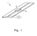
- Fig. 1 is a perspective view illustrating an RFID tag produced according to an embodiment of the present invention.
- An RFID tag 1 illustrated in Fig. 1 includes a base 11 in which a metal antenna pattern 112 is formed on a film 111 made of a PET material, an IC chip 12 mounted on the base 11, and a thermosetting adhesive 13p which bonds the base 11 and IC chip 12.
- the RFID tag 1 of this embodiment is an electronic apparatus which contactlessly exchanges information with a reader writer, which is not illustrated, and receives energy of an electromagnetic field, which the reader writer emits, as electric energy by the antenna pattern 112. Then, the IC chip 12 is driven with the electric energy.
- the antenna pattern 112 functions as an antenna for communication, and the IC chip 12 executes radio communication through the antenna pattern 112.
- the RFID tag 1 is equivalent to an example of the electronic apparatus of the present invention
- the antenna pattern 112 is equivalent to an example of the conductor pattern of the present invention
- the IC chip 12 is equivalent to an example of the circuit chip of the present invention.
- the "RFID tag” used in the specification of the present application may be called an “inlay for an RFID tag” which is an internal construction member (inlay) for the "RFID tag.”
- this "RFID tag” may be called a “wireless IC tag.”
- a noncontact IC card is also included in this "RFID tag.”
- Fig. 2 is an explanatory diagram of the production method of the RFID tag illustrated in Fig. 1 .
- Fig. 2 illustrates each step of producing the RFID tag in order from Part (a) to Part (e).
- Fig. 2 illustrates each step of producing the RFID tag in order from Part (a) to Part (e).
- dimensions of the RFID tag 1 in a thickness direction and the IC chip 12 are exaggeratedly expressed in comparison with those illustrated in Fig. 1 .
- two or more RFID tags are formed side by side on one sheet of long film, and RFID tags are completed by separating the film into respective individual RFID tags. But, here, a production method will be described paying attention to one RFID tag.
- the base 11 in which the antenna pattern 112 is formed on the film 111 made of a PET material is prepared, and the liquid thermosetting adhesive 13p is made to adhere to this base 11.
- the thermosetting adhesive 13p is applied to an area for mounting the IC chip 12 and its vicinity on a mounting surface 11a which the antenna pattern 112 of the base 11 is formed on.
- thermosetting adhesive 13p of this embodiment for example, an epoxy adhesive is adopted, and in further detail, an anoxic-anhydrous epoxy adhesive whose curing rate, that is, a ratio of components to be cured is not less than 90% when being heated on curing conditions of 190°C and 8 sec is adopted. Nevertheless, as the thermosetting adhesive 13p, a resin material which has thermosetting property is adoptable besides the anoxic-anhydrous epoxy adhesive.
- the thermosetting adhesive 13p of this embodiment exerts practical strength when a curing rate is not less than 90%.
- the curing conditions of 190°C and 8 sec in the thermosetting adhesive 13p are called practical curing condition.
- the IC chip 12 is mounted on the portion of the base 11, to which the thermosetting adhesive 13p is adhered, at a mounting step illustrated in Part (b) and Part (c) of Fig. 2 .
- the IC chip 12 is mounted on the base 11 by a flip chip assembly technique. That is, the IC chip 12 is mounted on the base 11 through the thermosetting adhesive 13p such that a face 12a of the IC chip 12, on which the circuit is formed, faces the base 11. Bumps 121 connected to the antenna pattern 112 are formed also on the face 12a.
- the IC chip 12 is mounted on the base 11 in a state where the bumps 121 are aligned with the antenna pattern 112.
- the base 11 on which the IC chip 12 is mounted is clamped and pressurized by a heating apparatus 2 from both of the film 111 side and the IC chip 12 side.
- the heating apparatus 2 has a heating head 21 as a hold-down section and a heating stage 22 as a supporting section, so that the base 11 is held between the heating head 21 and the heating stage 22.
- the heating head 21 embeds a heater which is not illustrated.
- the heating head 21 abuts the 1C chip 12, and the heating stage 22 abuts the film 111.
- the heating head 21 is made to generate heat and preheats the thermosetting adhesive 13p on the first heating condition.
- the first heating condition of this embodiment is set as a condition by which the thermosetting adhesive 13p starts a cure reaction, and has a curing rate of about 50% to become gel, that is, a semi hardened state.
- the first heating condition in this embodiment is 150°C and 8 sec, and is a lower temperature condition than the practical curing condition.
- the film 111 hardly deforms.
- the thermosetting adhesive 13p can be cured to the extent of having practical adhesive strength when it is applied for 30 sec even if a temperature is 150°C, a curing rate becomes about 50% by setting the time at 8 sec.
- a curing rate becomes about 50% by setting the time at 8 sec.
- To make the thermosetting adhesive 13p into a gel state where a curing rate is about 50% is also referred to as coming into a B stage. This gel state where the curing rate is about 50% is equivalent to an example of a first cured state
- the base 11 which is preheated is clamped and pressurized by a heating apparatus 3 from both of the film 111 side and the IC chip 12 side.
- the heating apparatus 3 also has a heating head 31 as a hold-down section, and a heating stage 32 as a supporting section such that the base 11 is held between the heating head 31 and the heating stage 32, and the heating head 31 embeds a heater which is not illustrated.
- the heating head 31 abuts on the IC chip 12, and the heating stage 32 abuts on the film 111.
- the heating head 31 is made to generate heat and preheats the thermosetting adhesive 13p on a second heating condition.
- the second heating condition of this embodiment is set at a condition by which a curing rate of the thermosetting adhesive 13p becomes not less than 90%.
- the thermosetting adhesive 13p has the curing rate of not less than 90% by being heated on the second heating condition, and has practical adhesive strength. This state where the curing rate is about 90% is equivalent to an example of a second cured state in the present invention.
- thermosetting adhesive 13p is cured to a state of the curing rate being not less than 90%.
- the preheating step is performed in the production method of this embodiment, and a temperature condition which is lower than the temperature condition of the second heating condition, is used as the first temperature condition at the preheating step. For this reason, when performing heating at the main heating step, the thermosetting adhesive 13p is already gel. Thus, flow of the thermosetting adhesive 13p is suppressed when heating the thermosetting adhesive 13p at the main heating step, and generation of a void is suppressed.
- the RFID tag 1 illustrated in Fig. 1 is obtained by cooling the base 11 with the circuit chip 12 mounted after the main heating step.
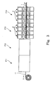
- Fig. 3 is a diagram illustrating a production line which performs the production method of RFID tags, illustrated in Fig. 2 , in a flow process.
- Fig. 3 illustrates roughly the production line which produces two or more RFID tags using the one sheet of long film-shaped base.
- two or more antenna patterns 112 (refer to Fig. 2 ) corresponding to two or more RFID tags are located and formed in a line at predetermined intervals on the one sheet of long film 111 (refer to Fig. 2 ).
- Two or more RFID tags are produced by passing through an adhesion step P11, a mounting step P12, a preheating step P13, and a main heating step P14 in this order while a base 11 is conveyed in the conveying direction D.
- Each of the adhesion step P11, mounting step P12, preheating step P13, and actual heating step P14 performs processing for four RFID tags at once.
- heating apparatuses 2 and four heating apparatuses 3 are arranged at the preheating step P13 and actual heating step P14, respectively. Respective steps proceed in parallel simultaneously, and a period of performing processing at each step is called a processing cycle. Whenever one processing cycle is executed, the base 11 is conveyed in the conveying direction D by a portion corresponding to four RFID tags. RFID tags are produced successively by repeating the processing cycle.
- thermosetting adhesive 13p is applied to the base 11 at the adhesion step P11, as illustrated in Part (a) of Fig. 2 .
- the IC chip 12 is mounted on the portion of the base 11, which the thermosetting adhesive 13p is applied to, at the mounting step P12 as illustrated in Part (b) and Part (c) of Fig. 2 .
- the base 11 is preheated on the first heating condition.
- the heating apparatus 2 is heated to a temperature corresponding to the first heating condition, and the heating apparatus 2 clamps the base 11 for a time corresponding to the first heating condition.
- the base 11 is heated on the second heating condition.
- the heating apparatus 3 is heated to a temperature corresponding to the second heating condition, and the heating apparatus 3 clamps the base 11 for a time corresponding to the second heating condition.
- the RFID tags 1 are obtained by cutting the base 11 separately after the main heating step P14.
- heating apparatuses 2 arranged at the preheating step P13 and four heating apparatuses 3 arranged at the main heating step P14 are the same kind of heating apparatuses, but heating conditions, particularly, heating temperatures among heating conditions are different.
- Fig. 4 is an explanatory diagram of a production method of the second embodiment which produces the RFID tag illustrated in Fig. 1 .
- Fig. 4 illustrates each step of producing the RFID tag 1 in order from Part (a) to Part (e).
- the preheating step illustrated in Part (d) of Fig. 4 is different from the preheating step in the first embodiment.
- the thermosetting adhesive 13p is heated by causing infrared irradiation equipment 4 to radiate infrared rays.
- the infrared irradiation equipment 4 radiates infrared rays having strength sufficient for heating the thermosetting adhesive 13p at a temperature of 150°C which is the first heating condition.
- the thermosetting adhesive 13p is already gel.
- generation of a void is suppressed.
- Fig. 5 is a diagram illustrating a production line which performs the production of RFID tags, illustrated in Fig. 4 , in a flow process.
- Fig. 5 illustrates roughly the production line which produces two or more RFID tags using one sheet of long film-shaped base.
- an adhesion step P21, a mounting step P22, a preheating step P23, and a main heating step P24 are different from those in the production line illustrated in Fig. 3 , respectively.
- the infrared irradiation equipment 4 performs processing at the preheating step, all of the eight heating apparatuses are arranged at the main heating step P24.
- the production method is one embodiment of the production method of an article in which an electronic apparatus is mounted according to the present invention.
- Fig. 6 is an explanatory diagram of a production method of clothes in which an RFID tag is mounted.
- the RFID tag 1 produced by either of the production methods described in Fig. 2 to Fig. 5 is mounted by attachment and the like on a tag 5a of clothes 5 at a mounting step illustrated in Part (a) of Fig. 6 .
- information representing an attribute of the clothes 5 is stored in the RFID tag 1 mounted in the clothes 5 at a storage step illustrated in Part (b) of Fig. 6 .
- attribution information of the clothes 5, such as JAN code system is transmitted to the RFID tag 1 via radio communication from an information writing apparatus 6, and the attribution information is stored in the circuit chip 12 (refer to Fig. 1 ).
- Fig. 7 illustrates a printed circuit board apparatus produced according to one embodiment of the present invention, and a cellular phone in which this printed circuit board apparatus is packaged.
- the cellular phone 7 illustrated in Fig. 7 has a telephone body section 71, and a printed circuit board apparatus 75 packaged in the telephone body section 71.
- the printed circuit board apparatus 75 has a flexible printed circuit 77 (FPC 77) as a base, and a circuit chip 76 fixed to the FPC 77 with a thermosetting adhesive.
- the telephone body section 71 is provided with a display section 71a which is driven on the basis of an operation of the circuit chip 76, and shows various displays.
- the printed circuit board apparatus 75 is produced by a method similar to the production methods of the RFID tag 1 illustrated in Fig. 2 to Fig. 5 . That is, the printed circuit board apparatus 75 has a thin structure in which a circuit chip is mounted on a base made of a film, through a thermosetting adhesive, and is produced by passing through an adhesion step, a mounting step, a preheating step, and a main heating step in this order.
- the printed circuit board apparatus 75 is packaged in the telephone body section 71.
- the printed circuit board apparatus 75 has a thin form but is reliable, because it is produced by a method of suppressing the generation of a void.
- the present invention is not limited to these.
- the present invention may be applied to a production method of an ultrathin IC card, and the like, for example, so long as it is a production method of an electronic apparatus in which a circuit chip is mounted on a film-shaped base.
- a film which constitutes a base of an RFID tag is described as that made of a PET material in the embodiments mentioned above, a film of an electronic apparatus of the present invention is not limited to this.
- a film may be formed of a material selected from a polyester material, a polyolefine material, a polycarbonate material, an acrylic material, and the like.
- a heating time for pressurizing the base 11 and a time for heating the thermosetting adhesive 13p by the heating apparatus 2 or 3 are the same, the preheating step and heating step of the present invention are not limited to this.
- the base after pressurizing a base by a heating apparatus, the base may be heated.
Landscapes
- Engineering & Computer Science (AREA)
- Microelectronics & Electronic Packaging (AREA)
- Computer Hardware Design (AREA)
- Physics & Mathematics (AREA)
- General Physics & Mathematics (AREA)
- Theoretical Computer Science (AREA)
- Encapsulation Of And Coatings For Semiconductor Or Solid State Devices (AREA)
- Wire Bonding (AREA)
- Credit Cards Or The Like (AREA)
Applications Claiming Priority (1)
| Application Number | Priority Date | Filing Date | Title |
|---|---|---|---|
| JP2007043183A JP2008209961A (ja) | 2007-02-23 | 2007-02-23 | 電子装置の製造方法、電子装置が実装された電子機器の製造方法、および、電子装置が装着された物品の製造方法 |
Publications (2)
| Publication Number | Publication Date |
|---|---|
| EP1962231A2 true EP1962231A2 (de) | 2008-08-27 |
| EP1962231A3 EP1962231A3 (de) | 2009-02-25 |
Family
ID=39512581
Family Applications (1)
| Application Number | Title | Priority Date | Filing Date |
|---|---|---|---|
| EP07124166A Withdrawn EP1962231A3 (de) | 2007-02-23 | 2007-12-28 | Herstellungsverfahren für eine elektronische Vorrichtung, Herstellungsverfahren für elektronische Geräte mit der darin enthaltenen elektronischen Vorrichtung und Herstellungsverfahren für einen Gegenstand mit der darin montierten elektronischen Vorrichtung |
Country Status (6)
| Country | Link |
|---|---|
| US (1) | US20080202678A1 (de) |
| EP (1) | EP1962231A3 (de) |
| JP (1) | JP2008209961A (de) |
| KR (1) | KR20080078538A (de) |
| CN (1) | CN101252094A (de) |
| TW (1) | TW200836603A (de) |
Cited By (3)
| Publication number | Priority date | Publication date | Assignee | Title |
|---|---|---|---|---|
| EP4084048A4 (de) * | 2019-12-26 | 2023-06-07 | Sato Holdings Kabushiki Kaisha | Ic-chip-montagevorrichtung und ic-chip-montageverfahren |
| US12568787B2 (en) | 2019-12-26 | 2026-03-03 | Sato Corporation | IC chip mounting device and IC chip mounting method |
| US12588532B2 (en) | 2019-12-26 | 2026-03-24 | Sato Corporation | IC chip mounting device, and IC chip mounting method |
Families Citing this family (4)
| Publication number | Priority date | Publication date | Assignee | Title |
|---|---|---|---|---|
| USD589828S1 (en) * | 2007-01-15 | 2009-04-07 | Murata Manufacturing Co., Ltd. | IC tag inlet |
| CN102204419A (zh) * | 2008-10-31 | 2011-09-28 | 东丽株式会社 | 电子部件和挠性薄膜基板的接合方法及接合装置 |
| TWI417525B (zh) * | 2009-11-12 | 2013-12-01 | 具有無線射頻系統標籤之溫度感測貼片 | |
| TWI564106B (zh) * | 2011-03-28 | 2017-01-01 | 山田尖端科技股份有限公司 | 接合裝置以及接合方法 |
Citations (1)
| Publication number | Priority date | Publication date | Assignee | Title |
|---|---|---|---|---|
| JP2001156110A (ja) | 1999-11-24 | 2001-06-08 | Omron Corp | 半導体チップの実装方法、並びに、電磁波読み取り可能なデータキャリアの製造方法 |
Family Cites Families (9)
| Publication number | Priority date | Publication date | Assignee | Title |
|---|---|---|---|---|
| US6333206B1 (en) * | 1996-12-24 | 2001-12-25 | Nitto Denko Corporation | Process for the production of semiconductor device |
| JP3402267B2 (ja) * | 1999-06-23 | 2003-05-06 | ソニーケミカル株式会社 | 電子素子の実装方法 |
| JP4311862B2 (ja) * | 2000-05-29 | 2009-08-12 | 東レエンジニアリング株式会社 | チップ実装方法 |
| JP3665579B2 (ja) * | 2001-02-26 | 2005-06-29 | ソニーケミカル株式会社 | 電気装置製造方法 |
| JP3753984B2 (ja) * | 2002-01-09 | 2006-03-08 | シャープ株式会社 | 非接触通信機器用モジュール及びその製造方法 |
| JP3750606B2 (ja) * | 2002-01-11 | 2006-03-01 | ソニーケミカル株式会社 | 半導体装置の製造方法 |
| JP2004213259A (ja) * | 2002-12-27 | 2004-07-29 | Konica Minolta Holdings Inc | Icカード、icカード製造方法及びicカード製造装置並びにicカード判定システム |
| JP4672384B2 (ja) * | 2004-04-27 | 2011-04-20 | 大日本印刷株式会社 | Icタグ付シートの製造方法、icタグ付シートの製造装置、icタグ付シート、icチップの固定方法、icチップの固定装置、およびicタグ |
| TWI339358B (en) * | 2005-07-04 | 2011-03-21 | Hitachi Ltd | Rfid tag and manufacturing method thereof |
-
2007
- 2007-02-23 JP JP2007043183A patent/JP2008209961A/ja active Pending
- 2007-12-25 TW TW096149879A patent/TW200836603A/zh unknown
- 2007-12-28 EP EP07124166A patent/EP1962231A3/de not_active Withdrawn
- 2007-12-28 US US11/966,434 patent/US20080202678A1/en not_active Abandoned
-
2008
- 2008-01-17 CN CNA2008100018705A patent/CN101252094A/zh active Pending
- 2008-01-17 KR KR1020080005308A patent/KR20080078538A/ko not_active Abandoned
Patent Citations (1)
| Publication number | Priority date | Publication date | Assignee | Title |
|---|---|---|---|---|
| JP2001156110A (ja) | 1999-11-24 | 2001-06-08 | Omron Corp | 半導体チップの実装方法、並びに、電磁波読み取り可能なデータキャリアの製造方法 |
Cited By (4)
| Publication number | Priority date | Publication date | Assignee | Title |
|---|---|---|---|---|
| EP4084048A4 (de) * | 2019-12-26 | 2023-06-07 | Sato Holdings Kabushiki Kaisha | Ic-chip-montagevorrichtung und ic-chip-montageverfahren |
| EP4485524A3 (de) * | 2019-12-26 | 2025-04-23 | Sato Holdings Kabushiki Kaisha | Ic-chip-anbringeinrichtung und ic-chip-anbringverfahren |
| US12568787B2 (en) | 2019-12-26 | 2026-03-03 | Sato Corporation | IC chip mounting device and IC chip mounting method |
| US12588532B2 (en) | 2019-12-26 | 2026-03-24 | Sato Corporation | IC chip mounting device, and IC chip mounting method |
Also Published As
| Publication number | Publication date |
|---|---|
| TW200836603A (en) | 2008-09-01 |
| CN101252094A (zh) | 2008-08-27 |
| US20080202678A1 (en) | 2008-08-28 |
| EP1962231A3 (de) | 2009-02-25 |
| KR20080078538A (ko) | 2008-08-27 |
| JP2008209961A (ja) | 2008-09-11 |
Similar Documents
| Publication | Publication Date | Title |
|---|---|---|
| EP1956873B1 (de) | RFID-Etikett und Herstellungsverfahren dafür | |
| EP1962231A2 (de) | Herstellungsverfahren für eine elektronische Vorrichtung, Herstellungsverfahren für elektronische Geräte mit der darin enthaltenen elektronischen Vorrichtung und Herstellungsverfahren für einen Gegenstand mit der darin montierten elektronischen Vorrichtung | |
| JP7562624B2 (ja) | 電子部品が埋め込まれた取引カード及び製造プロセス | |
| KR101107943B1 (ko) | 전자 장치, 전자 장치가 실장된 전자 기기, 전자 장치가 장착된 물품, 및 전자 장치의 제조 방법 | |
| KR100816107B1 (ko) | Rfid 태그의 제조 방법, 및 rfid 태그 | |
| US7789316B2 (en) | Electronic device, electronic apparatus mounted with electronic device, article equipped with electronic device and method of producing electronic device | |
| US7982295B2 (en) | Electronic device, electronic apparatus mounted with electronic device, article equipped with electronic device and method of producing electronic device | |
| US20100243743A1 (en) | Radio frequency identification tag and method for manufacturing the same | |
| KR20080068530A (ko) | 전자 장치의 제조 방법 | |
| EP1947687A2 (de) | Verfahren und Vorrichtung zur Herstellung einer elektronischen Vorrichtung | |
| EP1947918B1 (de) | Elektronische Vorrichtung und Herstellungsverfahren dafür | |
| KR20250043415A (ko) | 층상 전자 장치 및 이를 제조하는 방법 | |
| KR20100043945A (ko) | 무선 인식 태그의 제조 방법 및 제조 장치 |
Legal Events
| Date | Code | Title | Description |
|---|---|---|---|
| PUAI | Public reference made under article 153(3) epc to a published international application that has entered the european phase |
Free format text: ORIGINAL CODE: 0009012 |
|
| AK | Designated contracting states |
Kind code of ref document: A2 Designated state(s): AT BE BG CH CY CZ DE DK EE ES FI FR GB GR HU IE IS IT LI LT LU LV MC MT NL PL PT RO SE SI SK TR |
|
| AX | Request for extension of the european patent |
Extension state: AL BA HR MK RS |
|
| PUAL | Search report despatched |
Free format text: ORIGINAL CODE: 0009013 |
|
| AK | Designated contracting states |
Kind code of ref document: A3 Designated state(s): AT BE BG CH CY CZ DE DK EE ES FI FR GB GR HU IE IS IT LI LT LU LV MC MT NL PL PT RO SE SI SK TR |
|
| AX | Request for extension of the european patent |
Extension state: AL BA HR MK RS |
|
| AKX | Designation fees paid | ||
| REG | Reference to a national code |
Ref country code: DE Ref legal event code: 8566 |
|
| STAA | Information on the status of an ep patent application or granted ep patent |
Free format text: STATUS: THE APPLICATION IS DEEMED TO BE WITHDRAWN |
|
| 18D | Application deemed to be withdrawn |
Effective date: 20090826 |