EP1957397B1 - Verfahren zur herstellung von kohlenstoffnanoröhren(cnt)-paste und emitter mit hoher zuverlässigkeit - Google Patents
Verfahren zur herstellung von kohlenstoffnanoröhren(cnt)-paste und emitter mit hoher zuverlässigkeit Download PDFInfo
- Publication number
- EP1957397B1 EP1957397B1 EP06823857.5A EP06823857A EP1957397B1 EP 1957397 B1 EP1957397 B1 EP 1957397B1 EP 06823857 A EP06823857 A EP 06823857A EP 1957397 B1 EP1957397 B1 EP 1957397B1
- Authority
- EP
- European Patent Office
- Prior art keywords
- cnt
- paste
- metal particles
- emitter
- cnt paste
- Prior art date
- Legal status (The legal status is an assumption and is not a legal conclusion. Google has not performed a legal analysis and makes no representation as to the accuracy of the status listed.)
- Not-in-force
Links
Images
Classifications
-
- B—PERFORMING OPERATIONS; TRANSPORTING
- B82—NANOTECHNOLOGY
- B82B—NANOSTRUCTURES FORMED BY MANIPULATION OF INDIVIDUAL ATOMS, MOLECULES, OR LIMITED COLLECTIONS OF ATOMS OR MOLECULES AS DISCRETE UNITS; MANUFACTURE OR TREATMENT THEREOF
- B82B3/00—Manufacture or treatment of nanostructures by manipulation of individual atoms or molecules, or limited collections of atoms or molecules as discrete units
-
- H—ELECTRICITY
- H01—ELECTRIC ELEMENTS
- H01J—ELECTRIC DISCHARGE TUBES OR DISCHARGE LAMPS
- H01J9/00—Apparatus or processes specially adapted for the manufacture, installation, removal, maintenance of electric discharge tubes, discharge lamps, or parts thereof; Recovery of material from discharge tubes or lamps
- H01J9/02—Manufacture of electrodes or electrode systems
- H01J9/022—Manufacture of electrodes or electrode systems of cold cathodes
- H01J9/025—Manufacture of electrodes or electrode systems of cold cathodes of field emission cathodes
-
- H—ELECTRICITY
- H01—ELECTRIC ELEMENTS
- H01J—ELECTRIC DISCHARGE TUBES OR DISCHARGE LAMPS
- H01J1/00—Details of electrodes, of magnetic control means, of screens, or of the mounting or spacing thereof, common to two or more basic types of discharge tubes or lamps
- H01J1/02—Main electrodes
- H01J1/30—Cold cathodes, e.g. field-emissive cathode
- H01J1/304—Field-emissive cathodes
-
- B—PERFORMING OPERATIONS; TRANSPORTING
- B22—CASTING; POWDER METALLURGY
- B22F—WORKING METALLIC POWDER; MANUFACTURE OF ARTICLES FROM METALLIC POWDER; MAKING METALLIC POWDER; APPARATUS OR DEVICES SPECIALLY ADAPTED FOR METALLIC POWDER
- B22F2999/00—Aspects linked to processes or compositions used in powder metallurgy
-
- B—PERFORMING OPERATIONS; TRANSPORTING
- B82—NANOTECHNOLOGY
- B82Y—SPECIFIC USES OR APPLICATIONS OF NANOSTRUCTURES; MEASUREMENT OR ANALYSIS OF NANOSTRUCTURES; MANUFACTURE OR TREATMENT OF NANOSTRUCTURES
- B82Y40/00—Manufacture or treatment of nanostructures
-
- C—CHEMISTRY; METALLURGY
- C22—METALLURGY; FERROUS OR NON-FERROUS ALLOYS; TREATMENT OF ALLOYS OR NON-FERROUS METALS
- C22C—ALLOYS
- C22C26/00—Alloys containing diamond or cubic or wurtzitic boron nitride, fullerenes or carbon nanotubes
- C22C2026/002—Carbon nanotubes
-
- H—ELECTRICITY
- H01—ELECTRIC ELEMENTS
- H01J—ELECTRIC DISCHARGE TUBES OR DISCHARGE LAMPS
- H01J2201/00—Electrodes common to discharge tubes
- H01J2201/30—Cold cathodes
- H01J2201/304—Field emission cathodes
- H01J2201/30446—Field emission cathodes characterised by the emitter material
- H01J2201/30453—Carbon types
-
- H—ELECTRICITY
- H01—ELECTRIC ELEMENTS
- H01J—ELECTRIC DISCHARGE TUBES OR DISCHARGE LAMPS
- H01J2201/00—Electrodes common to discharge tubes
- H01J2201/30—Cold cathodes
- H01J2201/304—Field emission cathodes
- H01J2201/30446—Field emission cathodes characterised by the emitter material
- H01J2201/30453—Carbon types
- H01J2201/30469—Carbon nanotubes (CNTs)
Definitions
- the present invention relates to methods of manufacturing carbon nanotube (CNT) paste which has nano-sized metal particles as a metal filler, and a CNT emitter with high reliability.
- CNT carbon nanotube
- LCDs liquid crystal displays
- PDPs plasma display panels
- FEDs field emission displays
- FEDs follow similar physical principles to CRTs, except that electron emitters of CRTs are formed of a cold cathode material.
- a cathode a very fine field emitter
- FEDs can be manufactured lightweight and thin still with an excellent display characteristic.
- FEDs are ideal in all aspects of the display device, so that they are attracting attention as the next generation display devices with the most potential.
- Carbon nanotubes have recently been in the limelight as electron emitters of such FEDs.
- the CNTs provide the most excellent performance as emitters using a field emission principle in which an electron is emitted when an electric field is applied to a pointy conductive emitter in a vacuum state.
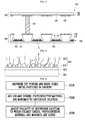
- FIG. 1 is a schematic cross-sectional view of an FED using a conventional CNT emitter. An operation principle of the FED using CNT will now be described with reference to FIG. 1 .
- the FED 100 includes an electron emission part 110 in which an emitter 114 is formed as an electron emitter, and an image display part 130 which has a fluorescent layer 135 generating light by colliding the light emitted from the electron emission part 110 with a fluorescent material.
- the image display part 130 includes a second substrate 131, an anode 133 formed on the second substrate 131, fluorescent layers 135 formed on the anode 133 to be spaced apart from each other, and a light shielding layer 137 formed between the fluorescent layers 135.
- the light shielding layer 137 serves as a boundary between pixels.
- the electron emission part 110 includes a first substrate 111, cathodes 113 formed on the first substrate 111 to be spaced apart from each other in a predetermined shape, a CNT emitter 114 manufactured using CNT on the cathode 113, and a gate electrode 119 insulated from and adjacent to the cathode 113.
- An insulating layer 118 is formed under the gate electrode 119.
- a spacer 140 is disposed between the electron emission part 110 and the image display part 130 to support them.
- CNT paste first has to be manufactured.
- the CNT paste may be manufactured by the steps of: (1) dispersing CNT and a metal filler; (2) adding an organic binder and a photosensitive resin; and (3) mixing the added materials using a solvent and adjusting its viscosity.
- the CNT paste manufactured by steps (1) to (3) is applied onto the cathode 113 of the electron emission part 110, and then exposed and patterned, and thus the CNT emitter 114 may be completed.
- the CNT emitter 114 is manufactured using the above-described CNT paste, there is a limitation to performance of the FED because adhesion between the cathode 113 and the CNT emitter 114 is not uniform, and thus resistance between the cathode 113 and the CNT emitter 114 or between CNTs of the CNT emitter 114 becomes high or non-uniform. That is, since the CNT emitter 114 is not formed on the cathode 113 with strong adhesion, when a strong electric field is generated in the CNT emitter 114, the CNT emitter 114 may be detached from the cathode 113.
- contact resistance between the CNT emitter 114 and the cathode 113 may be non-uniform or increased, and only some of the CNT emitters 114 contribute to electron emission, thereby deteriorating an electron emission characteristic, which results in a decrease in electron emission sites and non-uniform distribution of electron emission. Also, since the resistance between the CNTs of the CNT emitter 114 may not be uniform, only some of the CNT emitters 114 serve to emit electrons, and thus a lifespan of the CNT emitter 114 drastically decreases.
- FIG. 2 is a partial cross-sectional view of an enlarged region II of the CNT emitter 114 of FIG. 1 , in which the role of the metal filler 115 added to the CNT paste is reinforced.
- the submicrometer-sized metal filler 115 illustrated in FIG. 2 is significantly larger than the CNT 117, a dispersion degree in the CNT paste is not only very weak, but agglomeration A of the metal filler 115 and the CNT 117 may also occur. To reduce the agglomeration A, the metal filler 115 is made as small as possible, and thereby the non-uniform degree of dispersion between the metal filler 115 and the CNT 117 may be partially overcome.
- the problems of the adhesion between the cathode 113 and the CNT emitter 114, and the resistance non-uniformity between the cathode 113 and the CNT emitter 114 or between the CNTs of the CNT emitter 114 may not be thoroughly resolved only by reducing the size of the metal filler 115.
- the metal particles have a size of 0.5-1.0 ⁇ m.
- the metal particles have a size of 1-500nm.
- the concentration of the CNT powder in the CNT paste is 1-30wt%.
- the concentration of the metal particles in the CNT paste is 0.1-20wt%.
- the metal particles have a size of 0.01-100 ⁇ m
- the ratio of the weight percentages of the CNT powder and the metal particles in the CNT paste is not indicated.
- the concentration of the CNT powder in the CNT paste is about 0.01-6.0wt%.
- the concentration of the metal particles in the CNT paste is about 3-15wt% (cf. page 8).
- the ratio of the weight percentage of the CNT powder and the metal particles in the CNT paste may be 80/20, 60/40, 40/60 and 20/80 (cf. page 16).
- the present invention is directed to a method of manufacturing carbon nanotube (CNT) paste improving adhesion between a CNT emitter and a cathode by adding a nano-sized metal particle which is meltable at a low temperature at which CNTs do not deteriorate.
- CNT carbon nanotube
- the present invention is directed to a method of manufacturing a CNT emitter with high reliability, which can improve uniformity of electron emission and increase electron emission sites by using CNT paste having a nano-sized metal particle.
- the present invention provides a method of manufacturing carbon nanotube (CNT) paste as defined in present claim 1.
- the present invention may further comprise the step of adding a photosensitive material and a monomer which is polymerized with the organic binder by reacting with the photosensitive material in the mixed dispersion solution.
- the metal particle When the metal particle is formed in a powder type, the metal particle may be added in step (i), whereas, when the metal particle is formed in a paste type, the metal particle may be added in step (iii).
- the metal particle is melted at a lower temperature than a deterioration point of the CNT powder.
- the metal particle may comprise Ag, Ru, Ti, Pd, Zn, Fe, or Au, which has excellent conductivity.
- the deterioration temperature of the CNT powder may be between 400 and 550°C.
- the solvent may have a good surface active characteristic, and be formed of isopropyl alcohol (IPA) and terpineol.
- IPA isopropyl alcohol
- terpineol isopropyl alcohol
- the present invention also provides a method of manufacturing a CNT emitter as defined in present claim 8.
- the step of plasticizing the CNT paste may comprise at least one of the steps of: plasticizing the CNT paste at about 250 to 300°C in an atmosphere; and plasticizing the CNT paste at about 320 to 450°C in a vacuum.
- step of plasticizing the CNT paste in an atmosphere burning-out of the organic binder and melting of the metal particle may be performed.
- step of plasticizing the CNT paste in a vacuum carbonization of the remaining organic binder and additional melting of the metal particle may be performed.
- a rolling treatment in which glue does not get leftover may be performed.
- a nano-sized metal particle capable of being melted at a low temperature at which carbon nanotubes (CNTs) do not deteriorate is added, thereby improving adhesion between a CNT emitter and a cathode.
- CNT paste is evenly mixed in a conductor with excellent conductivity due to the melted metal particles, and thus the CNT emitter and the metal particle are stably adhered to a field emission device (FED), which induces uniform electron emission.
- FED field emission device
- the adhesion between the CNT emitter and the cathode is improved by the melted metal particles, thereby reducing resistance between the cathode and the CNT, or between the CNTs.
- the electron emission may be constantly maintained, and the density of an active emission site contributing to the electron emission may be increased, and thus the CNT emitter with high reliability may be provided.
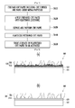
- FIG. 3 is a block diagram illustrating a method of manufacturing carbon nanotube (CNT) paste according to the present invention.
- CNT carbon nanotube
- the metal particle may have a size of several or several tens of nanometers, and be formed in a powder or paste type.
- the powdery metal particles are used.
- the step of dispersing the powdery metal particles together with the CNT powder is disclosed herein, the CNT paste may be manufactured using paste-type metal particles. In this case, the paste-type metal particles are added in a milling step that is a subsequent process.
- the metal particle may be a highly conductive metal capable of making an ohmic contact to lower interface resistances between the CNTs, and between the CNT and a cathode (not illustrated) of the CNT emitter formed using the CNT paste.
- the highly conductive metals usable for the CNT paste include Ag, Ti, Pd, Zn, Au, Fe and Ru, which are individually used or properly mixed for use. Since the nano-sized metal particle is formed by mixing various metals, its adhesion and electrical characteristics may be improved.
- the CNT powder and the nano-sized metal particles can be dispersed in most solvents such as a water-soluble solvent, an organic solvent, etc.
- solvents such as a water-soluble solvent, an organic solvent, etc.
- the solvent preferably has a good surface active characteristic. It is preferable that an additional solvent having a high temperature for vaporization (boiling point: about 150°C or more) is used together to protect rapid evaporation.
- the CNT powder and the nano-sized metal particles are dispersed in isopropyl alcohol (IPA) and terpineol which have a good surface active characteristic.
- IPA isopropyl alcohol
- terpineol which have a good surface active characteristic.
- the CNT powder and the nano-sized metal particles are included with an appropriate composition ratio in consideration of a configuration of the CNT emitter to be manufactured employing the same.
- a composition ratio of the CNT powder to the metal particle is 1:2.
- an organic binder, a photosensitive material and a monomer are added to the dispersion solution in which the CNT powder and the nano-sized metal particles are dispersed (S320).
- the organic binder added to the dispersion solution various kinds of polymers such as acryl resin series or ethyl cellulose may be commonly used.
- the photosensitive material directs the monomer to react when receiving light, which may be selected depending on the kind of the added organic binder, and particularly, a material matched with the organic binder may be preferably selected.
- the monomer is a material added to obtain a patterning characteristic by exposure, which serves to be polymerized with a polymer by being initiated by the photosensitive material.
- the photosensitive material has to be optimized with an appropriate weight ratio of the monomer to the organic binder, and if the ratio is not appropriate, it may affect the final configuration of the CNT emitter.
- the photosensitive material is added to have a weight ratio ranging from 1/10 to 1/100 of the organic binder, and the monomer is added to have the same ratio as the photosensitive material.
- the photosensitive material is mixed in the CNT paste, the CNT paste applied on the substrate or electrode may be formed in a specific shape by exposure.
- the CNT paste may be patterned by a screen printing method when the photosensitive material is not added. In this case, the patterning is more effective to form a large pattern of 100 ⁇ m or more.
- the viscosity of the dispersion solution, to which the organic binder, the photoresist material, and the monomer are added, is adjusted (S330).
- a milling process is used to adjust the viscosity of the dispersion solution.
- FIG. 4 is a block diagram illustrating a method of manufacturing a CNT emitter using the CNT paste manufactured in FIG. 3 ;
- FIG. 5A is an enlarged cross-sectional view schematically illustrating a CNT emitter patterned with a CNT paste to which a nano-sized metal particle is added according to an exemplary embodiment of the present invention; and
- FIG. 5B is an enlarged cross-sectional view schematically illustrating a CNT emitter completed after the step of plasticizing the CNT emitter of FIG. 3 .
- CNT paste 530 including CNT powder 531 and nano-sized metal particles 532 is first prepared (S410).
- the process of manufacturing the CNT paste 530 refers to the steps of FIG. 3 (from S310 to S330).
- the CNT paste 530 is applied onto an electrode 520 (a cathode) formed on a substrate 510 of a field emission device (FED) (S420).
- FED field emission device
- the CNT paste 530 applied onto the cathode 520 is exposed and patterned in a desired pattern (S430).
- the patterned CNT paste 530 is plasticized (S440).
- the step of plasticizing the CNT paste 530 includes a first plasticizing process performed at about 250 to 300°C in the atmosphere, and a second plasticizing process performed at about 320 to 450°C in a vacuum.
- an organic binder included in the CNT paste 530 can be burned out, and the metal particles can be melted depending on the kind of the metal particle.
- the metal particles may be melted under the above-mentioned conditions (in a vacuum and at a temperature of 320 to 450°C).
- the melting point of metal depends on the relative ratio between a surface area of the metal particle and a weight of the metal particle.
- Metal commonly having a melting point of 800°C can be melted at about 400°C, which is half the melting point, if the metal particle becomes smaller than ⁇ m or less, whereas it can be melted at about 100°C, if the metal particle is split into several to several tens nm size. These characteristics may depend on the kind of metal and the surrounding of a melting particle.
- a surface of the plasticized CNT paste 500 is surface-treated to be activated (S450).
- various methods may be used, such as a plasma treatment, a high field treatment, a taping treatment and a rolling treatment.
- the rolling treatment is preferable because it removes an out-gassing problem in a vacuum and glue does not get leftover.
- the CNT emitter 500 manufactured through the above-described steps unlike the conventional CNT emitter illustrated in FIG. 2 , nano-sized metal particles 532a and nano-sized CNTs 531 are evenly dispersed. Also, a contact between the CNTs may be uniformly made by the melted metal and the FED, which includes the CNT emitter 500 having an improved electron emission characteristic through the physical surface treatment steps, can be finally manufactured. Particularly, when the CNT emitter 500 is manufactured through the manufacturing process, the emitter may have an ideal configuration so that its adhesion is far more improved than when it is simply adhered with a metal filler, thereby reducing electrical resistance and improving uniformity thereof.
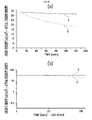
- FIGs. 6A and 6B are graphs respectively illustrating electron emission char acteristics and uniformity of current density versus time between the CNT emitter manufactured according to the present invention and the CNT manufactured according to the conventional art.
- FIG. 6A is a graph illustrating an electron emission characteristic, in which an x axis represents time, a y axis represents current density, and continuous electron emission is performed at a DC voltage.
- Graph (I) shows an electron emission characteristic of the CNT emitter manufactured using CNT paste according to the present invention
- graph (II) shows an electron emission characteristic of the CNT emitter manufactured using CNT paste according to conventional art.
- initial current densities in the both graphs are about 30mA/cm 2 . In the beginning of measuring the current density, the CNT emitter according to the present invention and the CNT emitter according to the conventional art have almost the same current density.
- the CNT emitter according to the present invention has a current density of about 30mA/cm 2
- the conventional CNT emitter has a current density of about 19mA/cm 2 after two hours. That is, it can be noted that the CNT emitter manufactured according to the present invention uniformly emits electrons as compared with the conventional CNT emitter in an environment of continuous electron emission for about two hours.
- FIG. 6B is a graph illustrating uniformity of current density, in which an x axis represents time (log scale), and a y axis represents current density.
- Graph (I') shows uniformity of current density of the CNT emitter manufactured using the CNT paste according to the present invention
- graph (II') shows uniformity of current density of the CNT paste according to the conventional art. It can be noted that the current density according to graph (I') is almost constant, but the current density according to graph (II') is reduced as the time goes on.
Landscapes
- Engineering & Computer Science (AREA)
- Manufacturing & Machinery (AREA)
- Chemical & Material Sciences (AREA)
- Crystallography & Structural Chemistry (AREA)
- Nanotechnology (AREA)
- Cold Cathode And The Manufacture (AREA)
- Conductive Materials (AREA)
Claims (12)
- Verfahren zur Herstellung von Kohlenstoff-Nanoröhrchen-(CNT-)Paste (530), umfassend die folgenden Schritte:(i) Dispergieren von CNT-Pulver (531) in einem Lösungsmittel (Schritt S310);(ii) Hinzufügen eines organischen Binders in die Lösung, in der das CNT-Pulver dispergiert ist (Schritt S320); und(iii) Durchführen eines Zerkleinerungsprozesses zum Anpassen der Viskosität der Dispersionslösung, in die der organische Binder hinzugefügt ist (Schritt S330),
wobei Nanogrößen-Metallpartikel (532) im Schritt (i) oder (iii) hinzugefügt werden;
wobei die Nanogrößen-Metallpartikel (532) eine Größe von mehreren oder mehreren zehn Nanometer haben; und
wobei das CNT-Pulver (531) und die Metallpartikel (532) die CNT-Paste (530) mit einem Gewichtsprozentanteil von 1:2 bilden;
derart, dass die Metallpartikel (532) in der Lage sind, bei einer niedrigen Temperatur geschmolzen zu werden, bei der sich das CNT-Pulver (531) nicht verschlechtert. - Verfahren nach Anspruch 1, ferner umfassend den Schritt (iv) des Hinzufügens eines fotosensitiven Materials und eines Monomers, das mit dem organischen Binder durch Reaktion mit dem fotosensitiven Material in der gemischten Dispersionslösung polymerisiert wird.
- Verfahren nach Anspruch 1, wobei dann, wenn die Metallpartikel (532) als Pulvertyp gebildet sind, die Metallpartikel im Schritt (i) hinzugefügt werden.
- Verfahren nach Anspruch 1, wobei dann, wenn die Metallpartikel (532) als Pastentyp gebildet sind, die Metallpartikel (532) im Schritt (iii) hinzugefügt werden.
- Verfahren nach Anspruch 1, wobei die Metallpartikel (532) Ag, Ru, Ti, Pd, Zn, Fe oder Au umfassen, welches hervorragende Leitfähigkeit hat.
- Verfahren nach Anspruch 1, wobei das Lösungsmittel eine gute Oberflächenaktivitätseigenschaft hat.
- Verfahren nach Anspruch 6, wobei das Lösungsmittel Isopropylalkohol (IPA) und Terpineol enthält.
- Verfahren zur Herstellung eines CNT-Emitters, umfassend die Schritte:Herstellen einer CNT-Paste (530) durch das Herstellungsverfahren für CNT-Paste gemäß Anspruch 1 (Schritt S410);Aufbringen der CNT-Paste (530) auf eine Elektrode (520), die über einem Substrat (510) gebildet ist (Schritt S420);Belichten und Mustern der CNT-Paste (530), die auf die Elektrode (520) aufgebracht ist (Schritt S430);Plastifizieren der gemusterten CNT-Paste (530) bei einer Temperatur, bei der Metallpartikel (532) in der CNT-Paste geschmolzen werden, aber CNT-Pulver (531) in der CNT-Paste sich nicht verschlechtert (Schritt S440);Behandeln einer Oberfläche der plastifizierten CNT-Paste (530) zur Aktivierung (Schritt S450).
- Verfahren nach Anspruch 8, wobei der Schritt des Plastifizierens der CNT-Paste (530) (Schritt S440) wenigstens einen der folgenden Schritte umfasst:Plastifizieren der CNT-Paste (530) bei ungefähr 250 bis 300 Grad Celsius in einer Atmosphäre; undPlastifizieren der CNT-Paste (530) bei ungefähr 320 bis 450 Grad Celsius in einem Vakuum.
- Verfahren nach Anspruch 9, wobei im Schritt des Plastifizierens der CNT-Paste (530) in einer Atmosphäre ein Ausbrennen des organischen Binders und ein Schmelzen der Metallpartikel (532) durchgeführt werden.
- Verfahren nach Anspruch 10, wobei im Schritt des Plastifizierens der CNT-Paste (530) in einem Vakuum eine Karbonisierung des verbleibenden organischen Binders und zusätzliches Schmelzen der Metallpartikel (532) durchgeführt werden.
- Verfahren nach Anspruch 8, wobei im Schritt des Behandelns der Oberfläche der CNT-Paste (530) eine Walzbehandlung durchgeführt wird, bei der kein Kleber übrig bleibt.
Applications Claiming Priority (3)
| Application Number | Priority Date | Filing Date | Title |
|---|---|---|---|
| KR20050118182 | 2005-12-06 | ||
| KR1020060084912A KR100911370B1 (ko) | 2005-12-06 | 2006-09-05 | 고 신뢰성 cnt 페이스트의 제조 방법 및 cnt 에미터제조 방법 |
| PCT/KR2006/005149 WO2007066932A1 (en) | 2005-12-06 | 2006-12-01 | Methods of manufacturing carbon nanotube (cnt) paste and emitter with high reliability |
Publications (3)
| Publication Number | Publication Date |
|---|---|
| EP1957397A1 EP1957397A1 (de) | 2008-08-20 |
| EP1957397A4 EP1957397A4 (de) | 2009-09-09 |
| EP1957397B1 true EP1957397B1 (de) | 2015-04-15 |
Family
ID=38356165
Family Applications (1)
| Application Number | Title | Priority Date | Filing Date |
|---|---|---|---|
| EP06823857.5A Not-in-force EP1957397B1 (de) | 2005-12-06 | 2006-12-01 | Verfahren zur herstellung von kohlenstoffnanoröhren(cnt)-paste und emitter mit hoher zuverlässigkeit |
Country Status (5)
| Country | Link |
|---|---|
| EP (1) | EP1957397B1 (de) |
| JP (1) | JP4902666B2 (de) |
| KR (1) | KR100911370B1 (de) |
| CN (1) | CN101321687B (de) |
| WO (1) | WO2007066932A1 (de) |
Cited By (1)
| Publication number | Priority date | Publication date | Assignee | Title |
|---|---|---|---|---|
| DE102016013279A1 (de) | 2016-11-08 | 2018-05-09 | H&P Advanced Technology GmbH | Verfahren zur Herstellung eines Elektronenemitters mit einer Kohlenstoffnanoröhren enthaltenden Beschichtung |
Families Citing this family (17)
| Publication number | Priority date | Publication date | Assignee | Title |
|---|---|---|---|---|
| KR100777113B1 (ko) * | 2006-12-07 | 2007-11-19 | 한국전자통신연구원 | 미세패터닝이 가능한 고 신뢰성의 cnt 에미터 제조 방법 |
| KR101596372B1 (ko) | 2008-02-15 | 2016-03-08 | 삼성디스플레이 주식회사 | 표시장치용 투명전극, 표시장치 및 표시장치의 제조방법 |
| KR100977635B1 (ko) * | 2008-03-03 | 2010-08-23 | 주식회사 엑사이엔씨 | 페이스트 조성물, 이를 포함하는 저항체막 및 전자 부품 |
| DE102008053027A1 (de) * | 2008-10-24 | 2010-04-29 | Kme Germany Ag & Co. Kg | Verfahren zum Herstellen einer Kohlenstoff-Nanoröhren,Fullerene und/oder Graphene enthaltenden Beschichtung |
| KR101099237B1 (ko) | 2008-12-10 | 2011-12-27 | 엘에스전선 주식회사 | 전도성 페이스트와 이를 이용한 전도성 기판 |
| KR101078079B1 (ko) | 2008-12-10 | 2011-10-28 | 엘에스전선 주식회사 | 은 수식 탄소 나노튜브 함유 전도성 페이스트 조성물 |
| CN102262988A (zh) * | 2010-05-31 | 2011-11-30 | 海洋王照明科技股份有限公司 | 碳纳米管冷阴极的制造方法及其应用 |
| KR101795419B1 (ko) * | 2011-01-26 | 2017-11-13 | 주식회사 잉크테크 | 투명 도전막의 제조방법 및 이에 의해 제조된 투명 도전막 |
| CN103310869B (zh) * | 2012-03-08 | 2016-06-08 | 清华大学 | 碳纳米管浆料,其制备方法以及采用该碳纳米管浆料制备阴极发射体的方法 |
| KR101309537B1 (ko) | 2012-04-06 | 2013-10-14 | (주) 브이에스아이 | 카본나노튜브 페이스트 및 이의 제조방법 |
| KR101470096B1 (ko) | 2012-12-14 | 2014-12-05 | 현대자동차주식회사 | 나노복합재료 분산장치 |
| US9478385B2 (en) | 2013-11-26 | 2016-10-25 | Electronics And Telecommunications Research Institute | Field emission device having field emitter including photoelectric material and method of manufacturing the same |
| KR102032291B1 (ko) * | 2013-11-26 | 2019-11-08 | 한국전자통신연구원 | 광전물질이 포함된 전계방출 에미터를 갖는 전계방출소자 및 그 제조방법 |
| BR112018070583A2 (pt) | 2016-04-07 | 2019-02-05 | Molecular Rebar Design Llc | composições compreendendo uma pluralidade de nanotubos de carbono discretos, composição útil para tratar lençóis freáticos (groundwater) contaminados e processo para preparar a composição |
| CN106906469B (zh) * | 2017-04-25 | 2020-08-07 | 广东工业大学 | 一种微纳嵌套颗粒熔融自结合表面改性设备 |
| CN112242281B (zh) * | 2019-07-16 | 2022-03-22 | 清华大学 | 碳纳米管场发射体及其制备方法 |
| EP4075473A4 (de) * | 2019-12-30 | 2024-11-13 | Korea University Research and Business Foundation | Kohlenstoffnanoröhren-(cnt)-pastenemitter, verfahren zum herstellen desselben und röntgenröhrengerät, das denselben verwendet |
Family Cites Families (12)
| Publication number | Priority date | Publication date | Assignee | Title |
|---|---|---|---|---|
| KR100355389B1 (ko) * | 2000-05-26 | 2002-10-11 | 삼성에스디아이 주식회사 | 표면처리를 이용한 카본 나노튜브 필드 에미션 어레이의제조 방법 |
| US7449081B2 (en) * | 2000-06-21 | 2008-11-11 | E. I. Du Pont De Nemours And Company | Process for improving the emission of electron field emitters |
| US6436221B1 (en) * | 2001-02-07 | 2002-08-20 | Industrial Technology Research Institute | Method of improving field emission efficiency for fabricating carbon nanotube field emitters |
| KR100763890B1 (ko) * | 2001-08-06 | 2007-10-05 | 삼성에스디아이 주식회사 | Cnt를 적용한 전계방출표시소자의 제조방법 |
| US6811457B2 (en) * | 2002-02-09 | 2004-11-02 | Industrial Technology Research Institute | Cathode plate of a carbon nano tube field emission display and its fabrication method |
| JP2003249184A (ja) * | 2002-02-22 | 2003-09-05 | Hitachi Ltd | 電子源用ペースト、電子源およびこの電子源を用いた自発光パネル型表示装置 |
| TWI276140B (en) * | 2003-09-23 | 2007-03-11 | Ind Tech Res Inst | Method of forming carbon nanotube field emission source |
| KR20050060287A (ko) * | 2003-12-16 | 2005-06-22 | 삼성에스디아이 주식회사 | 카본나노튜브 에미터의 형성방법 |
| KR20050079339A (ko) * | 2004-02-05 | 2005-08-10 | 삼성에스디아이 주식회사 | 필드 에미터의 제조 방법 |
| JP2005222847A (ja) * | 2004-02-06 | 2005-08-18 | Hitachi Displays Ltd | 電子源用ペースト及びこの電子源用ペーストを用いた平面型画像表示装置 |
| JP2005222891A (ja) * | 2004-02-09 | 2005-08-18 | Hitachi Displays Ltd | 自発光型平面表示装置とその製造方法 |
| KR20050086237A (ko) * | 2004-02-25 | 2005-08-30 | 삼성에스디아이 주식회사 | 전자방출표시장치용 전자방출원의 형성방법과 이를 이용한전지방출표시장치 |
-
2006
- 2006-09-05 KR KR1020060084912A patent/KR100911370B1/ko not_active Expired - Fee Related
- 2006-12-01 WO PCT/KR2006/005149 patent/WO2007066932A1/en not_active Ceased
- 2006-12-01 JP JP2008544242A patent/JP4902666B2/ja not_active Expired - Fee Related
- 2006-12-01 CN CN2006800457538A patent/CN101321687B/zh not_active Expired - Fee Related
- 2006-12-01 EP EP06823857.5A patent/EP1957397B1/de not_active Not-in-force
Cited By (3)
| Publication number | Priority date | Publication date | Assignee | Title |
|---|---|---|---|---|
| DE102016013279A1 (de) | 2016-11-08 | 2018-05-09 | H&P Advanced Technology GmbH | Verfahren zur Herstellung eines Elektronenemitters mit einer Kohlenstoffnanoröhren enthaltenden Beschichtung |
| WO2018086737A1 (de) | 2016-11-08 | 2018-05-17 | Vilicus 142 Gmbh | Verfahren zur herstellung eines elektronenemitters mit einer nanostäbchen enthaltenden beschichtung |
| US10622180B2 (en) | 2016-11-08 | 2020-04-14 | Cetteen Gmbh | Method for producing an electron emitter coated with a nanorod-containing coating |
Also Published As
| Publication number | Publication date |
|---|---|
| CN101321687B (zh) | 2010-12-15 |
| KR20070059914A (ko) | 2007-06-12 |
| EP1957397A1 (de) | 2008-08-20 |
| CN101321687A (zh) | 2008-12-10 |
| JP4902666B2 (ja) | 2012-03-21 |
| WO2007066932A1 (en) | 2007-06-14 |
| KR100911370B1 (ko) | 2009-08-10 |
| JP2009518806A (ja) | 2009-05-07 |
| EP1957397A4 (de) | 2009-09-09 |
Similar Documents
| Publication | Publication Date | Title |
|---|---|---|
| CN101221872B (zh) | 具有高可靠性的可精细构图的碳纳米管发射体的制造方法 | |
| WO2007066932A1 (en) | Methods of manufacturing carbon nanotube (cnt) paste and emitter with high reliability | |
| US20080299298A1 (en) | Methods of Manufacturing Carbon Nanotube (Cnt) Paste and Emitter with High Reliability | |
| US6436221B1 (en) | Method of improving field emission efficiency for fabricating carbon nanotube field emitters | |
| JP4262976B2 (ja) | 電子電界エミッタの放出状態を改善するための方法 | |
| Youh et al. | Flat panel light source with lateral gate structure based on SiC nanowire field emitters | |
| KR20100086468A (ko) | 전하 소산층을 갖는 언더게이트 전계 방출 트라이오드 | |
| US10026584B2 (en) | Method for making carbon nanotube slurry | |
| Cho et al. | Characterizations of fine-pitched carbon nanotube pixels for field emitter arrays | |
| US7855496B2 (en) | Boron nitride nanotube paste composition, electron emission source including the same, electron emission device including the electron emission source, and backlight unit and electron emission display device including the electron emission device | |
| KR20050087265A (ko) | 나노 크기의 금속 입자가 첨가된 탄소나노튜브 에미터 및그 제조 방법 | |
| KR100814838B1 (ko) | 전계 방출 소자의 카본 나노튜브 에미터 형성용 조성물 및그 제조 방법 | |
| Kim et al. | Fabrication of carbon nanotube paste using photosensitive polymer for field emission display | |
| KR100932976B1 (ko) | 평판표시소자의 전자 방출원 형성용 슬러리 조성물 및이를 이용한 전극 형성 방법 | |
| KR101100817B1 (ko) | 카본계 물질 및 나노 사이즈를 갖는 금속 입자의 용융물을포함한 전자 방출원, 이를 포함한 전자 방출 소자 및 상기전자 방출원 형성용 조성물 | |
| KR20140142200A (ko) | 전계방출용 에미터용 탄소나노튜브 페이스트, 이를 이용한 에미터 및 전계방출소자 | |
| KR100965545B1 (ko) | 평판 표시 소자의 전자 방출원 형성용 조성물 및 이로부터형성된 전자 방출원 | |
| JP4984130B2 (ja) | ナノカーボンエミッタとその製造方法並びに面発光素子 | |
| KR20080047917A (ko) | 전자 방출원용 카본계 물질, 이를 포함한 전자 방출원,상기 전자 방출원을 구비한 전자 방출 소자 및 상기 전자방출원의 제조 방법 | |
| KR20080083472A (ko) | 전자 방출 디바이스, 및 이의 제조 방법 | |
| KR20170018175A (ko) | 탄소나노튜브를 이용한 전계방출원의 제조방법 |
Legal Events
| Date | Code | Title | Description |
|---|---|---|---|
| PUAI | Public reference made under article 153(3) epc to a published international application that has entered the european phase |
Free format text: ORIGINAL CODE: 0009012 |
|
| 17P | Request for examination filed |
Effective date: 20080409 |
|
| AK | Designated contracting states |
Kind code of ref document: A1 Designated state(s): AT BE BG CH CY CZ DE DK EE ES FI FR GB GR HU IE IS IT LI LT LU LV MC NL PL PT RO SE SI SK TR |
|
| A4 | Supplementary search report drawn up and despatched |
Effective date: 20090806 |
|
| RIC1 | Information provided on ipc code assigned before grant |
Ipc: H01J 1/304 20060101ALI20090731BHEP Ipc: H01J 9/02 20060101AFI20090731BHEP |
|
| 17Q | First examination report despatched |
Effective date: 20091029 |
|
| DAX | Request for extension of the european patent (deleted) | ||
| GRAP | Despatch of communication of intention to grant a patent |
Free format text: ORIGINAL CODE: EPIDOSNIGR1 |
|
| INTG | Intention to grant announced |
Effective date: 20141118 |
|
| GRAS | Grant fee paid |
Free format text: ORIGINAL CODE: EPIDOSNIGR3 |
|
| GRAA | (expected) grant |
Free format text: ORIGINAL CODE: 0009210 |
|
| AK | Designated contracting states |
Kind code of ref document: B1 Designated state(s): AT BE BG CH CY CZ DE DK EE ES FI FR GB GR HU IE IS IT LI LT LU LV MC NL PL PT RO SE SI SK TR |
|
| REG | Reference to a national code |
Ref country code: GB Ref legal event code: FG4D Ref country code: CH Ref legal event code: EP |
|
| REG | Reference to a national code |
Ref country code: IE Ref legal event code: FG4D |
|
| REG | Reference to a national code |
Ref country code: AT Ref legal event code: REF Ref document number: 722384 Country of ref document: AT Kind code of ref document: T Effective date: 20150515 |
|
| REG | Reference to a national code |
Ref country code: DE Ref legal event code: R096 Ref document number: 602006045160 Country of ref document: DE Effective date: 20150528 |
|
| REG | Reference to a national code |
Ref country code: NL Ref legal event code: VDEP Effective date: 20150415 |
|
| REG | Reference to a national code |
Ref country code: AT Ref legal event code: MK05 Ref document number: 722384 Country of ref document: AT Kind code of ref document: T Effective date: 20150415 |
|
| REG | Reference to a national code |
Ref country code: LT Ref legal event code: MG4D |
|
| PG25 | Lapsed in a contracting state [announced via postgrant information from national office to epo] |
Ref country code: NL Free format text: LAPSE BECAUSE OF FAILURE TO SUBMIT A TRANSLATION OF THE DESCRIPTION OR TO PAY THE FEE WITHIN THE PRESCRIBED TIME-LIMIT Effective date: 20150415 |
|
| PG25 | Lapsed in a contracting state [announced via postgrant information from national office to epo] |
Ref country code: PT Free format text: LAPSE BECAUSE OF FAILURE TO SUBMIT A TRANSLATION OF THE DESCRIPTION OR TO PAY THE FEE WITHIN THE PRESCRIBED TIME-LIMIT Effective date: 20150817 Ref country code: FI Free format text: LAPSE BECAUSE OF FAILURE TO SUBMIT A TRANSLATION OF THE DESCRIPTION OR TO PAY THE FEE WITHIN THE PRESCRIBED TIME-LIMIT Effective date: 20150415 Ref country code: ES Free format text: LAPSE BECAUSE OF FAILURE TO SUBMIT A TRANSLATION OF THE DESCRIPTION OR TO PAY THE FEE WITHIN THE PRESCRIBED TIME-LIMIT Effective date: 20150415 Ref country code: LT Free format text: LAPSE BECAUSE OF FAILURE TO SUBMIT A TRANSLATION OF THE DESCRIPTION OR TO PAY THE FEE WITHIN THE PRESCRIBED TIME-LIMIT Effective date: 20150415 |
|
| PG25 | Lapsed in a contracting state [announced via postgrant information from national office to epo] |
Ref country code: IS Free format text: LAPSE BECAUSE OF FAILURE TO SUBMIT A TRANSLATION OF THE DESCRIPTION OR TO PAY THE FEE WITHIN THE PRESCRIBED TIME-LIMIT Effective date: 20150815 Ref country code: LV Free format text: LAPSE BECAUSE OF FAILURE TO SUBMIT A TRANSLATION OF THE DESCRIPTION OR TO PAY THE FEE WITHIN THE PRESCRIBED TIME-LIMIT Effective date: 20150415 Ref country code: AT Free format text: LAPSE BECAUSE OF FAILURE TO SUBMIT A TRANSLATION OF THE DESCRIPTION OR TO PAY THE FEE WITHIN THE PRESCRIBED TIME-LIMIT Effective date: 20150415 Ref country code: GR Free format text: LAPSE BECAUSE OF FAILURE TO SUBMIT A TRANSLATION OF THE DESCRIPTION OR TO PAY THE FEE WITHIN THE PRESCRIBED TIME-LIMIT Effective date: 20150716 |
|
| REG | Reference to a national code |
Ref country code: DE Ref legal event code: R097 Ref document number: 602006045160 Country of ref document: DE |
|
| PG25 | Lapsed in a contracting state [announced via postgrant information from national office to epo] |
Ref country code: DK Free format text: LAPSE BECAUSE OF FAILURE TO SUBMIT A TRANSLATION OF THE DESCRIPTION OR TO PAY THE FEE WITHIN THE PRESCRIBED TIME-LIMIT Effective date: 20150415 Ref country code: EE Free format text: LAPSE BECAUSE OF FAILURE TO SUBMIT A TRANSLATION OF THE DESCRIPTION OR TO PAY THE FEE WITHIN THE PRESCRIBED TIME-LIMIT Effective date: 20150415 |
|
| PLBE | No opposition filed within time limit |
Free format text: ORIGINAL CODE: 0009261 |
|
| STAA | Information on the status of an ep patent application or granted ep patent |
Free format text: STATUS: NO OPPOSITION FILED WITHIN TIME LIMIT |
|
| PG25 | Lapsed in a contracting state [announced via postgrant information from national office to epo] |
Ref country code: CZ Free format text: LAPSE BECAUSE OF FAILURE TO SUBMIT A TRANSLATION OF THE DESCRIPTION OR TO PAY THE FEE WITHIN THE PRESCRIBED TIME-LIMIT Effective date: 20150415 Ref country code: RO Free format text: LAPSE BECAUSE OF NON-PAYMENT OF DUE FEES Effective date: 20150415 Ref country code: PL Free format text: LAPSE BECAUSE OF FAILURE TO SUBMIT A TRANSLATION OF THE DESCRIPTION OR TO PAY THE FEE WITHIN THE PRESCRIBED TIME-LIMIT Effective date: 20150415 Ref country code: SK Free format text: LAPSE BECAUSE OF FAILURE TO SUBMIT A TRANSLATION OF THE DESCRIPTION OR TO PAY THE FEE WITHIN THE PRESCRIBED TIME-LIMIT Effective date: 20150415 |
|
| 26N | No opposition filed |
Effective date: 20160118 |
|
| PG25 | Lapsed in a contracting state [announced via postgrant information from national office to epo] |
Ref country code: IT Free format text: LAPSE BECAUSE OF FAILURE TO SUBMIT A TRANSLATION OF THE DESCRIPTION OR TO PAY THE FEE WITHIN THE PRESCRIBED TIME-LIMIT Effective date: 20150415 |
|
| PG25 | Lapsed in a contracting state [announced via postgrant information from national office to epo] |
Ref country code: BE Free format text: LAPSE BECAUSE OF NON-PAYMENT OF DUE FEES Effective date: 20151231 Ref country code: SI Free format text: LAPSE BECAUSE OF FAILURE TO SUBMIT A TRANSLATION OF THE DESCRIPTION OR TO PAY THE FEE WITHIN THE PRESCRIBED TIME-LIMIT Effective date: 20150415 |
|
| PG25 | Lapsed in a contracting state [announced via postgrant information from national office to epo] |
Ref country code: MC Free format text: LAPSE BECAUSE OF FAILURE TO SUBMIT A TRANSLATION OF THE DESCRIPTION OR TO PAY THE FEE WITHIN THE PRESCRIBED TIME-LIMIT Effective date: 20150415 Ref country code: LU Free format text: LAPSE BECAUSE OF FAILURE TO SUBMIT A TRANSLATION OF THE DESCRIPTION OR TO PAY THE FEE WITHIN THE PRESCRIBED TIME-LIMIT Effective date: 20151201 |
|
| REG | Reference to a national code |
Ref country code: CH Ref legal event code: PL |
|
| GBPC | Gb: european patent ceased through non-payment of renewal fee |
Effective date: 20151201 |
|
| PG25 | Lapsed in a contracting state [announced via postgrant information from national office to epo] |
Ref country code: BE Free format text: LAPSE BECAUSE OF FAILURE TO SUBMIT A TRANSLATION OF THE DESCRIPTION OR TO PAY THE FEE WITHIN THE PRESCRIBED TIME-LIMIT Effective date: 20150415 |
|
| REG | Reference to a national code |
Ref country code: IE Ref legal event code: MM4A |
|
| REG | Reference to a national code |
Ref country code: FR Ref legal event code: ST Effective date: 20160831 |
|
| PG25 | Lapsed in a contracting state [announced via postgrant information from national office to epo] |
Ref country code: GB Free format text: LAPSE BECAUSE OF NON-PAYMENT OF DUE FEES Effective date: 20151201 Ref country code: CH Free format text: LAPSE BECAUSE OF NON-PAYMENT OF DUE FEES Effective date: 20151231 Ref country code: IE Free format text: LAPSE BECAUSE OF NON-PAYMENT OF DUE FEES Effective date: 20151201 Ref country code: LI Free format text: LAPSE BECAUSE OF NON-PAYMENT OF DUE FEES Effective date: 20151231 |
|
| PG25 | Lapsed in a contracting state [announced via postgrant information from national office to epo] |
Ref country code: FR Free format text: LAPSE BECAUSE OF NON-PAYMENT OF DUE FEES Effective date: 20151231 |
|
| PG25 | Lapsed in a contracting state [announced via postgrant information from national office to epo] |
Ref country code: BG Free format text: LAPSE BECAUSE OF FAILURE TO SUBMIT A TRANSLATION OF THE DESCRIPTION OR TO PAY THE FEE WITHIN THE PRESCRIBED TIME-LIMIT Effective date: 20150415 Ref country code: HU Free format text: LAPSE BECAUSE OF FAILURE TO SUBMIT A TRANSLATION OF THE DESCRIPTION OR TO PAY THE FEE WITHIN THE PRESCRIBED TIME-LIMIT; INVALID AB INITIO Effective date: 20061201 |
|
| PG25 | Lapsed in a contracting state [announced via postgrant information from national office to epo] |
Ref country code: CY Free format text: LAPSE BECAUSE OF FAILURE TO SUBMIT A TRANSLATION OF THE DESCRIPTION OR TO PAY THE FEE WITHIN THE PRESCRIBED TIME-LIMIT Effective date: 20150415 Ref country code: SE Free format text: LAPSE BECAUSE OF FAILURE TO SUBMIT A TRANSLATION OF THE DESCRIPTION OR TO PAY THE FEE WITHIN THE PRESCRIBED TIME-LIMIT Effective date: 20150415 |
|
| PG25 | Lapsed in a contracting state [announced via postgrant information from national office to epo] |
Ref country code: TR Free format text: LAPSE BECAUSE OF FAILURE TO SUBMIT A TRANSLATION OF THE DESCRIPTION OR TO PAY THE FEE WITHIN THE PRESCRIBED TIME-LIMIT Effective date: 20150415 |
|
| PGFP | Annual fee paid to national office [announced via postgrant information from national office to epo] |
Ref country code: DE Payment date: 20231120 Year of fee payment: 18 |
|
| REG | Reference to a national code |
Ref country code: DE Ref legal event code: R119 Ref document number: 602006045160 Country of ref document: DE |
|
| PG25 | Lapsed in a contracting state [announced via postgrant information from national office to epo] |
Ref country code: DE Free format text: LAPSE BECAUSE OF NON-PAYMENT OF DUE FEES Effective date: 20250701 |