EP1944614A1 - Semiconductor inspection system and apparatus utilizing a non-vibrating contact potential difference sensor and controlled illumination - Google Patents
Semiconductor inspection system and apparatus utilizing a non-vibrating contact potential difference sensor and controlled illumination Download PDFInfo
- Publication number
- EP1944614A1 EP1944614A1 EP08250761A EP08250761A EP1944614A1 EP 1944614 A1 EP1944614 A1 EP 1944614A1 EP 08250761 A EP08250761 A EP 08250761A EP 08250761 A EP08250761 A EP 08250761A EP 1944614 A1 EP1944614 A1 EP 1944614A1
- Authority
- EP
- European Patent Office
- Prior art keywords
- wafer
- semiconductor
- sensor
- potential difference
- contact potential
- Prior art date
- Legal status (The legal status is an assumption and is not a legal conclusion. Google has not performed a legal analysis and makes no representation as to the accuracy of the status listed.)
- Ceased
Links
- 238000005286 illumination Methods 0.000 title claims abstract description 84
- 239000004065 semiconductor Substances 0.000 title claims abstract description 70
- 238000007689 inspection Methods 0.000 title description 5
- 239000000523 sample Substances 0.000 claims abstract description 88
- 238000000034 method Methods 0.000 claims abstract description 23
- 230000007547 defect Effects 0.000 claims abstract description 6
- 239000000356 contaminant Substances 0.000 claims description 18
- 238000001228 spectrum Methods 0.000 claims description 7
- 238000012512 characterization method Methods 0.000 claims description 3
- 239000002184 metal Substances 0.000 claims description 3
- 239000000126 substance Substances 0.000 claims description 2
- 238000005070 sampling Methods 0.000 claims 2
- 238000011109 contamination Methods 0.000 abstract description 14
- 238000009826 distribution Methods 0.000 abstract description 3
- 235000012431 wafers Nutrition 0.000 description 112
- 238000005259 measurement Methods 0.000 description 19
- 238000005452 bending Methods 0.000 description 13
- 230000000694 effects Effects 0.000 description 9
- 238000001514 detection method Methods 0.000 description 6
- 230000008859 change Effects 0.000 description 5
- 239000000463 material Substances 0.000 description 5
- 230000008569 process Effects 0.000 description 5
- 238000010586 diagram Methods 0.000 description 3
- 238000004519 manufacturing process Methods 0.000 description 3
- 239000003990 capacitor Substances 0.000 description 2
- 150000002500 ions Chemical class 0.000 description 2
- 238000012986 modification Methods 0.000 description 2
- 230000004048 modification Effects 0.000 description 2
- 230000003287 optical effect Effects 0.000 description 2
- 238000004886 process control Methods 0.000 description 2
- 230000004044 response Effects 0.000 description 2
- 238000009987 spinning Methods 0.000 description 2
- ZOXJGFHDIHLPTG-UHFFFAOYSA-N Boron Chemical compound [B] ZOXJGFHDIHLPTG-UHFFFAOYSA-N 0.000 description 1
- UFHFLCQGNIYNRP-UHFFFAOYSA-N Hydrogen Chemical compound [H][H] UFHFLCQGNIYNRP-UHFFFAOYSA-N 0.000 description 1
- VYPSYNLAJGMNEJ-UHFFFAOYSA-N Silicium dioxide Chemical compound O=[Si]=O VYPSYNLAJGMNEJ-UHFFFAOYSA-N 0.000 description 1
- XUIMIQQOPSSXEZ-UHFFFAOYSA-N Silicon Chemical compound [Si] XUIMIQQOPSSXEZ-UHFFFAOYSA-N 0.000 description 1
- 238000009825 accumulation Methods 0.000 description 1
- 230000015572 biosynthetic process Effects 0.000 description 1
- 229910052796 boron Inorganic materials 0.000 description 1
- 239000000969 carrier Substances 0.000 description 1
- 230000003749 cleanliness Effects 0.000 description 1
- 239000011248 coating agent Substances 0.000 description 1
- 238000000576 coating method Methods 0.000 description 1
- 239000004020 conductor Substances 0.000 description 1
- 230000001066 destructive effect Effects 0.000 description 1
- 230000005684 electric field Effects 0.000 description 1
- 238000005516 engineering process Methods 0.000 description 1
- 229910052739 hydrogen Inorganic materials 0.000 description 1
- 239000001257 hydrogen Substances 0.000 description 1
- 238000003384 imaging method Methods 0.000 description 1
- 238000000691 measurement method Methods 0.000 description 1
- 239000002245 particle Substances 0.000 description 1
- 230000035515 penetration Effects 0.000 description 1
- 230000006798 recombination Effects 0.000 description 1
- 238000005215 recombination Methods 0.000 description 1
- 230000035945 sensitivity Effects 0.000 description 1
- 229910052710 silicon Inorganic materials 0.000 description 1
- 239000010703 silicon Substances 0.000 description 1
- 229910052814 silicon oxide Inorganic materials 0.000 description 1
- 239000002356 single layer Substances 0.000 description 1
- 230000003746 surface roughness Effects 0.000 description 1
- 230000007704 transition Effects 0.000 description 1
Images


Classifications
-
- H—ELECTRICITY
- H01—ELECTRIC ELEMENTS
- H01L—SEMICONDUCTOR DEVICES NOT COVERED BY CLASS H10
- H01L22/00—Testing or measuring during manufacture or treatment; Reliability measurements, i.e. testing of parts without further processing to modify the parts as such; Structural arrangements therefor
-
- G—PHYSICS
- G01—MEASURING; TESTING
- G01N—INVESTIGATING OR ANALYSING MATERIALS BY DETERMINING THEIR CHEMICAL OR PHYSICAL PROPERTIES
- G01N27/00—Investigating or analysing materials by the use of electric, electrochemical, or magnetic means
- G01N27/002—Investigating or analysing materials by the use of electric, electrochemical, or magnetic means by investigating the work function voltage
-
- G—PHYSICS
- G01—MEASURING; TESTING
- G01R—MEASURING ELECTRIC VARIABLES; MEASURING MAGNETIC VARIABLES
- G01R31/00—Arrangements for testing electric properties; Arrangements for locating electric faults; Arrangements for electrical testing characterised by what is being tested not provided for elsewhere
- G01R31/26—Testing of individual semiconductor devices
- G01R31/2648—Characterising semiconductor materials
-
- G—PHYSICS
- G01—MEASURING; TESTING
- G01R—MEASURING ELECTRIC VARIABLES; MEASURING MAGNETIC VARIABLES
- G01R31/00—Arrangements for testing electric properties; Arrangements for locating electric faults; Arrangements for electrical testing characterised by what is being tested not provided for elsewhere
- G01R31/26—Testing of individual semiconductor devices
- G01R31/265—Contactless testing
- G01R31/2656—Contactless testing using non-ionising electromagnetic radiation, e.g. optical radiation
Definitions
- the present invention is directed to methods and systems for the inspection of semiconductors and semiconductor surfaces. More particularly, the present invention is directed to a method and system for the characterization of non-uniformities through the use of a non-vibrating contact potential difference sensor in combination with a controllable illumination source to image and visualize the contact potential difference of the wafer surface.
- the Kelvin probe is a sensor that measures Contact Potential Difference (CPD).
- CPD is the difference in work function, or surface potential, of two conductive materials which are electrically connected.
- the Kelvin sensor consists of a conductive probe which is electrically connected to the surface to be measured. The probe is positioned close to the surface so that a capacitor is formed between the probe tip and the surface. A potential difference (voltage) results from the CPD between the probe tip and the surface.
- the probe tip is positioned at a point above the surface and then vibrated perpendicular to the surface so that the capacitance between the probe tip and the surface varies with time.
- This varying capacitance results in a time-varying current into the probe tip which is proportional to the voltage between the probe tip and the surface.
- This current is amplified to facilitate detection, and a variable bias voltage, sometimes called a backing voltage, is applied to the probe such that the time varying current goes to zero.
- the bias voltage is equal and opposite to the CPD, so the CPD is determined.
- Many variations of the Kelvin probe have been developed. These include the Monroe probe, which vibrates a shutter in front of the probe tip instead of vibrating the tip itself; and scanning probes which make vibrating measurements at a series of points across a surface by stepping from one point to the next or moving slowly while the probe is vibrated.
- the probe can be operated with a fixed, or no, bias voltage and the magnitude of the probe current can be calibrated and converted to surface potential values.
- the signal is generated by varying the capacitance between the probe tip and the surface using vibration.
- Kelvin probes are very useful in the characterization of many surfaces, including semiconductor surfaces.
- the Kelvin probe is useful because the work function of a surface, and resulting surface potential and CPD, are very sensitive to a wide range of surface conditions that can affect semiconductor device quality; such as contamination, surface chemistry, atomic surface roughness and surface charging.
- the Kelvin probe is essentially a point measurement technique. Although multiple measurements can be made at different points on a surface, or a series of adjacent points can be measured in series, it is difficult to measure more than a few points per second. Generating high resolution images of whole semiconductor wafers is a slow and time consuming process that is not well-suited to real-time process control applications.
- a second method of characterizing a semiconductor utilizes Surface Photo Voltage (SPV).
- SPV Surface Photo Voltage
- the electrical potential of a semiconductor surface is often sensitive to illumination with specific frequencies of light.
- a semiconductor surface, or an interface between a semiconductor and another material will typically result in surface or interface-specific electron energy states. These states can cause surface charging and the formation of electric fields near the surface.
- This phenomenon of changing electrical potential near a semiconductor surface is known as band bending.
- Illumination of the semiconductor surface with sub-bandgap illumination can cause the population and depopulation of surface states that will also affect surface charging, band bending and the resulting surface potential.
- SPV-based tools have been developed to make a wide range of measurements on semiconductors and dielectric films on top of semiconductors.
- SPV measurements can be used to detect doping densities, characterize the degree of band bending or determine the density and position of electron energy states at semiconductor surfaces and interfaces.
- These systems sometimes include the ability to apply controlled amounts of charge to the surface of a dielectric film.
- SPV systems come in a variety of configurations with a range of measurement capabilities, these systems are all similar in that they make measurements by either 1) applying charge or illumination to the surface and then measuring the resulting surface potential or change in surface potential using a vibrating Kelvin probe, or 2) positioning a stationary capacitive probe over the surface and varying the charge or illumination to generate a time-varying signal that can be detected by the capacitive sensor. In other words, these systems generate a signal by varying the probe-to-surface capacitance, the illumination intensity, or the charge on the surface.
- SPV measurement systems are essentially point measurement systems, and are not suitable for the generation of high resolution, whole wafer images at production speeds.
- a third type of system for inspecting and measuring surfaces utilizes a non-vibrating contact potential difference sensor.
- the non-vibrating contact potential difference sensor consists of a conductive probe that is electrically connected to the semiconductor surface.
- the probe tip is positioned close to the surface to form a capacitor, and a potential difference is formed between the probe tip and the surface due to the difference in work functions or surface potentials.
- the non-vibrating contact potential difference sensor does not vibrate perpendicular to the surface. Instead, the probe tip is translated parallel to the surface, or the surface is translated beneath the probe. Changes in the work function or surface potential at different points on the surface result in changes in potential between the surface and the probe tip.
- the non-vibrating contact potential difference sensor can acquire surface data at a much higher rate than the vibrating Kelvin probe because the signal is not formed by vibration of the probe, but is instead formed by the relative scanning motion between the probe and the surface.
- the non-vibrating contact potential difference sensor can provide a continuous stream of data at rates greater than 100,000 samples per second. High data acquisition rates permit high-resolution whole wafer images to be acquired in only a few minutes.
- the non-vibrating contact potential difference sensor While the non-vibrating contact potential difference sensor is well-suited to high-speed imaging of wafer surface potential, it produces data on only two wafer surface characteristics-changes in surface potential and changes in surface height. For semiconductor inspection applications, the sensor is usually operated to minimize the height signal by minimizing variations in the height of the probe above the wafer surface or minimizing the average potential between the probe tip and wafer surface. As a result, the non-vibrating contact potential difference sensor typically produces data on one characteristic of a surface-changes in surface potential.
- doping uniformity is an important characteristic of a semiconductor which affects many fundamental and critical semiconductor characteristics.
- it is difficult to identify doping density variations using the contact potential difference signal because the effect of doping density on work function is reduced or altered by surface or interface states that induce band bending near the wafer surface.
- doping density variations may be difficult to separate from other non-uniformities such as variations in surface chemistry and contamination.
- it would be desirable to improve the sensitivity of the non-vibrating contact potential difference sensor so that it could detect smaller or more subtle non-uniformities.
- the system and methods provide an enhanced non-vibrating contact potential difference sensor system that allows the sensor data to be used to detect bulk semiconductor non-uniformities, or to more easily detect and classify surface contaminants.
- semiconductor material susceptible to inspection by the system herein described will be denoted generally as a "wafer”.
- One embodiment includes a source of illumination that has variable intensity or spectrum of light output.
- the illumination source is used to illuminate the area under or near the non-vibrating contact potential difference sensor probe tip during scanning.
- information on surface potential variations is acquired when the surface is illuminated with one or more illumination conditions that are optimized for the detection and classification of specific surface or bulk wafer characteristics that affect the response of the surface potential to illumination.
- the apparatus consists of a non-vibrating contact potential difference sensor, a system for mechanically fixturing the wafer, a system for positioning the sensor a fixed distance above the wafer surface and generating relative motion between the probe tip and wafer surface such that the sensor probe tip moves parallel to the wafer surface, a source of illumination with variable intensity or spectrum of light that can irradiate the semiconductor wafer surface under or near the sensor probe tip, and a system for acquiring and processing the output signal from the sensor to identify and classify wafer non-uniformities.
- One embodiment of operation is as follows. First, a semiconductor wafer is placed and secured onto the fixture. The purpose of the fixture is to mechanically secure the wafer and to provide an electrical connection to the wafer surface. Because the non-vibrating contact potential difference sensor detects changes in surface potential, it is a time-varying signal. As a result, the contact between the fixture and wafer can be either capacitive or ohmic. The non-vibrating contact potential difference sensor probe tip is then positioned at a fixed height above the wafer surface. The wafer surface under or near the probe tip is illuminated with a specific intensity and spectrum of light and relative motion is generated between the probe tip and wafer surface such that the probe tip moves parallel to the wafer surface at a fixed height.
- the voltage between the probe tip and surface changes, resulting in a current into, or out of, the probe tip.
- This current is amplified and sampled to form a representation of variations in surface potential across the wafer.
- the wafer may be scanned one or more additional times with different intensities or wavelengths of illumination to form additional representations of variations in surface potential.
- the resulting data from the one or more scans is then processed to identify and classify areas of wafer non-uniformity.
- Figure 1 is a diagram of wafer scanning system with a non-vibrating contact potential difference sensor and a source of controlled illumination
- Figure 2a is a diagram of radial scanning operation
- Figure 2b illustrates a sample image from such a scanning operation
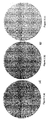
- Figure 3 illustrates non-vibrating contact potential difference images of a wafer with (a) super-bandgap illumination, (b) no illumination and (c) difference between Figures 3(a) and 3(b) ;
- Figures 4(a)-(c) illustrates non-vibrating contact potential difference images of the wafer shown in Figure 3(a)-(c) with processing to identify regions of non-uniformity.
- the present invention provides an enhanced non-vibrating contact potential difference sensor 10 1 system that allows the sensor data to be used to detect bulk semiconductor non-uniformities, such as but not limited to variations in doping density, that may cause the surface potential to be sensitive to illumination level.
- This invention is not limited to the measurement of semiconductors with bare, clean surfaces. The chemical state of the surface may vary, or surface contamination may be present.
- the wafer surface may be covered with a coating or film that permits illumination to penetrate through the film to the underlying semiconductor.
- a silicon wafer surface is often coated with a silicon oxide film which is transparent to some wavelengths of illumination.
- This invention can be used to inspect a wafer covered with a film to detect defects in the underlying semiconductor or at the semiconductor-film interface.
- this invention can be used to detect or classify defects in, or on, the film that affect band bending in the semiconductor or the response of the semiconductor surface to illumination.
- the apparatus consists of a non-vibrating contact potential difference sensor 101, a system 103 for mechanically fixturing the wafer 105, a system 107 for positioning the sensor 101 a fixed distance above the wafer surface 106 and generating relative motion between the probe tip 102 and wafer surface 106 such that the sensor probe tip 102 moves parallel to the wafer surface 106, a source of illumination 109 with variable intensity or spectrum of light that can irradiate the semiconductor wafer surface 106 under or near the sensor probe tip 102, and a system 111 for acquiring and processing the output signal from the sensor 101 to identify and classify wafer 105 non-uniformities.
- a semiconductor wafer 105 is placed on a conductive wafer fixture 103. This may be done manually or using an automated process such as, but limited to a wafer handling robot. The wafer 105 is held in place such as by using vacuum. Alternative methods of holding the wafer 105 include, but are not limited to, electrostatic forces and edge gripping.
- the fixture 103 is mounted to a spindle which can rotate the wafer 105 about its center.
- the non-vibrating contact potential difference sensor 101 is attached to a positioning system 107 that can adjust the height of the sensor 101 above the wafer surface 106 and can move the sensor 101 radially from at least the center of the wafer 105 to one edge of the wafer 105.
- the non-vibrating contact potential difference sensor 101 is electrically connected to the wafer surface 106 via the conductive wafer fixture 103. This connection can be resistive or capacitive.
- a height sensor 108 that has been calibrated to the height of the non-vibrating contact potential difference sensor probe tip 102 is also mounted on the same positioning system 107 as the non-vibrating CPD sensor 101.
- a light source 109 with variable intensity or variable wavelength is also mounted on the positioning system at an angle such that the illuminated area includes at least the area next to the non-vibrating contact potential difference sensor probe tip 102, with the illuminated area extending beneath the probe tip 102 to the extent allowed by the gap between the probe tip 102 and the wafer 105 and the angle of the light beam.
- the light source 109 can be a laser, incandescent lamp or other light source.
- a broadband light source may be coupled with a variable optical filter for selecting the desired wavelength and intensity of illumination.
- the non-vibrating contact potential difference sensor probe tip 102 may be transparent to illumination wavelengths to facilitate the illumination of the wafer surface 106 beneath the probe tip 102.
- the probe tip 102 may be shaped to facilitate illumination of the wafer surface 106 beneath the probe.
- the precise size and position of the illuminated spot is set so that the non-vibrating contact potential difference sensor 101 will scan over the illuminated area, which may include all or a large part of the wafer surface 106. If the light source 109 illuminates the entire wafer surface 106, or if it illuminates the entire area traversed by the sensor probe tip 102 during the scanning operation, then the light source 109 can be mounted in a fixed location and not on the positioning system 107.
- the height sensor 108 is positioned above one or more points on the wafer surface 106 and the height of the wafer surface 106 is measured. These wafer height measurements are used to calculate the position of the non-vibrating contact potential difference sensor 101 that will produce the desired distance between the probe tip 102 and the wafer surface 106. This information is used to position the probe tip 102 at a fixed height above the wafer surface 106, and the probe tip 102 is moved to a point above the outside edge of the wafer 105. Illumination is enabled and the appropriate intensity and wavelength are selected for the inspection application. For example, if the application is the detection of doping density, then a high intensity of super-bandgap illumination may be selected. If the application is surface contamination detection, then the intensity and wavelength appropriate for the likely contaminants are selected.
- the probe 101 is held stationary and the wafer 105 is rotated on the spindle such that the probe tip 102 moves above the wafer 105 along a circular path that is centered at the wafer 105 center.
- Data is acquired during a single rotation of the wafer 105.
- the sensor 101 is then moved a programmable distance along the radius of the wafer 105 towards the wafer center. Another rotation of data is acquired at this new radius.
- the probe tip 102 continues to step and scan concentric circular regions of the wafer 105 until the probe reaches the wafer center.
- the resulting data is then assembled into an image of the wafer 105. Alternately, each concentric circular region of the wafer 105 could be scanned multiple times and the resulting data averaged to reduce the effect of random noise.
- This image is processed to identify and classify non-uniformities.
- This processing can take many forms. It may be as simple as the thresholding of signal values to detect regions of the wafer surface 106 where the surface potential is changing relatively rapidly.
- the differential sensor data can also be integrated to generate an image which represents relative surface potential values. This integrated image can also be processed or thresholded to identify regions of high or low potential.
- Figure 2 illustrates a diagram of the radial scanning of one embodiment of the present invention.
- the non-vibrating contact potential difference sensor probe tip 102 is positioned at point "A" near the edge of the wafer 105.
- the wafer 105 is rotated on the wafer fixture 103 and a circular track of data is scanned.
- the probe tip 102 is moved a programmable distance towards the wafer 105 center to point "B" and a second circular track of data is scanned. This process is repeated until the probe tip 102 reaches the center of the wafer 105.
- the resulting data is combined into an image of the wafer surface 106.
- a sample image is shown as Figure 2b .
- One aspect of the invention relates to the detection of variations in doping density or bulk contamination in a semiconductor.
- Variations in doping density or bulk contamination can affect the Fermi level of the semiconductor, and the Fermi level directly affects the work function.
- band bending at the surface of the semiconductor may reduce the effect of Fermi level variations on work function changes.
- the wafer 105 may be illuminated with super bandgap illumination to reduce this band bending effect.
- the wafer surface 106 is then scanned using the non-vibrating contact potential difference sensor 101 to obtain data on surface potential and Fermi level changes across the wafer 105.
- the resulting data is processed to detect these variations which represent variations in doping density.
- the wafer 105 could be scanned with two different intensities of super-bandgap illumination, where one of the intensities might be 0, and the difference of the two scans calculated. This difference data could then be used to detect areas with different levels of band bending which would indicate variations in doping density.
- the non-vibrating contact potential difference sensor signal generated by other types of non-uniformities that don't affect band bending would not be sensitive to illumination. The signal from these types of non-uniformities would be eliminated by taking the difference of data generated with two different illumination intensities.
- a second aspect of this invention is the identification or classification of surface chemistry or contamination based on the effect of super bandgap illumination on surface work function.
- the effect of a fixed intensity of super bandgap illumination on the amount of band bending, and consequently its effect on work function, is dependant on the density and distribution of surface electron energy states that exist within the bandgap. These states are created by the termination of the semiconductor bulk at the surface, the reconfiguration of the semiconductor surface, molecules or atoms that chemically bond to the wafer surface 106 or molecules or atoms that adsorb on the wafer surface 106. Different surface conditions, such as hydrogen termination or oxide termination, different surface contaminants or adsorbed molecules, or dielectric films deposited on the surface of the wafer will generate different densities or distributions of surface states.
- Variations in surface state can result in variations in the magnitude of band bending at the surface.
- This invention permits the wafer surface 106 to be measured using the non-vibrating contact potential difference sensor 101 with an intensity of super bandgap illumination selected to maximize the difference in work function of the surface for contaminated and uncontaminated regions of the wafer 105, or to maximize the difference in work function of the surface between two different contaminants.
- the surface can be measured two or more times using different intensities of illumination that maximize the change in surface potential for contaminated or uncontaminated regions, or regions with different contaminants. The differences between these measurements can then be used to detect contaminants or classify different contaminants or surface conditions.
- a third aspect of this invention is the detection and classification of surface chemistry or contamination based on the effect of sub-bandgap illumination on surface work function.
- Sub bandgap illumination lacks sufficient energy to cause valence band electrons to jump directly to the conduction band. However, it can cause transitions from the valence band to a surface state or from a surface state to the conduction band. Illumination of the surface with sub-bandgap illumination of varying wavelengths can be used to populate and depopulate these gap states, resulting in changes in surface potential and work function. The change in surface potential with varying wavelengths of illumination is dependant on the surface condition and chemistry.
- This invention permits the wafer surface 106 to be measured using the non-vibrating contact potential difference sensor 101 with a wavelength of sub bandgap illumination selected to maximize the difference in work function of the surface for contaminated and uncontaminated regions of the wafer 105, or to maximize the difference in work function of the surface between two different contaminants.
- the surface can be measured two or more times using different wavelengths of illumination that maximize the change in work function for contaminated or uncontaminated regions, or regions with different contaminants. The differences in these measurements can then be used to detect contaminants or classify different contaminants or surface conditions.
- the wafer 105 may be scanned more than once, where the wavelength or intensity of illumination is altered between each scan. These scans can then be combined, for example by taking the difference, and the resulting data, processed to identify and classify surface or bulk non-uniformities. Scanning with two or more illumination conditions can be done by scanning the whole wafer 105 with one type of illumination, then changing the illumination and scanning the whole wafer 105 again, or it can be accomplished by scanning a single concentric circular path of data using one illumination condition, changing the illumination, rescanning the same path with the new illumination condition, and then repeating for all circular paths at each radius.
- the intensity or wavelength of the illumination can be changed during the scanning operation.
- the illumination can be switched on and off so that the varying illumination causes a change in surface potential at the switching frequency.
- the switching operation can be implemented by using an optical chopper that passes the illumination through a spinning disk with an alternating pattern of transparent and opaque features.
- the resulting illumination-induced surface potential signal can be separated from the signal created by the lateral motion of the non-vibrating contact potential difference sensor 101 relative to the wafer 105 by applying a frequency bandpass filter that passes the signal only at the switching frequency.
- the film surface can be charged with ions prior to measurement.
- the ions can be created via corona discharge or some other comparable method.
- Charging of the film surface can be used to bias the surface of the semiconductor into accumulation, depletion or inversion, which will affect band bending and SPV. This biasing charge can be applied and maintained at a constant level for all measurements, or it can be altered between sequential scans of the same wafer surface.
- the angle that the illumination energy contacts the wafer surface maybe controlled to provide for a desired depth of penetration into the wafer surface.
- Figure 3 illustrates non-vibrating contact potential difference images of a wafer 105.
- Figure 3(a) is super-bandgap illumination
- Figure 3(b) is with no illumination
- Figure 3(c) is the difference between that shown in Figure 3(a) and Figure 3(b) .
- the pattern in 3(c) is boron implanted into the wafer 105.
- the difference image shows a strong doping pattern and minimizes the signal from surface contaminants which are visible in (a) and (b).
- Figure 4 illustrates the non-vibrating contact potential difference images of the wafer 105 shown in Figures 3(a)-(c) with processing to identify regions of non-uniformity. The images have been processed by identifying regions of the image that fall above and below threshold values. Non-uniformity is clearly identified in Figure 4(c) , but is not distinguished from surface contamination in Figures 4(a) and 4(b) .
- the non-vibrating contact potential difference sensor 101, height sensor 108 and illumination source 109 could all be mounted at fixed locations, and the wafer 105 could be moved and rotated beneath these stationary elements.
- the non-vibrating contact potential difference sensor 101 could be moved continuously along the wafer 105 radius while the wafer 105 is spinning to create a continuous stream of data that spirals across the whole surface of the wafer 105.
- the non-vibrating contact potential difference sensor 101 could be moved linearly across the wafer 105 in a back-and-forth manner to scan the entire wafer surface 106.
- multiple non-vibrating contact potential difference sensors and illumination sources could be used to acquire multiple measurements simultaneously to reduce the time required to measure a wafer.
Landscapes
- Chemical & Material Sciences (AREA)
- Chemical Kinetics & Catalysis (AREA)
- Electrochemistry (AREA)
- Physics & Mathematics (AREA)
- Health & Medical Sciences (AREA)
- Life Sciences & Earth Sciences (AREA)
- Analytical Chemistry (AREA)
- Biochemistry (AREA)
- General Health & Medical Sciences (AREA)
- General Physics & Mathematics (AREA)
- Immunology (AREA)
- Pathology (AREA)
- Engineering & Computer Science (AREA)
- Manufacturing & Machinery (AREA)
- Computer Hardware Design (AREA)
- Microelectronics & Electronic Packaging (AREA)
- Power Engineering (AREA)
- Testing Or Measuring Of Semiconductors Or The Like (AREA)
- Investigating Or Analyzing Materials By The Use Of Electric Means (AREA)
Applications Claiming Priority (1)
| Application Number | Priority Date | Filing Date | Title |
|---|---|---|---|
| US11/715,149 US7659734B2 (en) | 2007-03-07 | 2007-03-07 | Semiconductor inspection system and apparatus utilizing a non-vibrating contact potential difference sensor and controlled illumination |
Publications (1)
| Publication Number | Publication Date |
|---|---|
| EP1944614A1 true EP1944614A1 (en) | 2008-07-16 |
Family
ID=39469573
Family Applications (1)
| Application Number | Title | Priority Date | Filing Date |
|---|---|---|---|
| EP08250761A Ceased EP1944614A1 (en) | 2007-03-07 | 2008-03-06 | Semiconductor inspection system and apparatus utilizing a non-vibrating contact potential difference sensor and controlled illumination |
Country Status (6)
| Country | Link |
|---|---|
| US (1) | US7659734B2 (enExample) |
| EP (1) | EP1944614A1 (enExample) |
| JP (1) | JP4783801B2 (enExample) |
| KR (1) | KR100929768B1 (enExample) |
| CN (1) | CN101266222A (enExample) |
| TW (1) | TWI346776B (enExample) |
Cited By (1)
| Publication number | Priority date | Publication date | Assignee | Title |
|---|---|---|---|---|
| US9304160B1 (en) | 2012-05-08 | 2016-04-05 | Kla-Tencor Corporation | Defect inspection apparatus, system, and method |
Families Citing this family (10)
| Publication number | Priority date | Publication date | Assignee | Title |
|---|---|---|---|---|
| US7944550B2 (en) * | 2008-02-29 | 2011-05-17 | International Business Machines Corporation | System and method for detecting local mechanical stress in integreated devices |
| CN102292804B (zh) * | 2009-02-03 | 2014-02-12 | Q概念技术公司 | 利用非振动接触势差传感器的图案化晶片检查系统 |
| US8441268B2 (en) * | 2010-04-06 | 2013-05-14 | Lam Corporation | Non-contact detection of surface fluid droplets |
| US20170266744A1 (en) * | 2015-10-30 | 2017-09-21 | Mitsubishi Electric Corporation | Wire electric discharge machine, control method of control device of wire electric discharge machine, and positioning method |
| CN108760885A (zh) * | 2018-06-14 | 2018-11-06 | 德淮半导体有限公司 | 超声波扫描方法和超声波扫描装置 |
| US10859625B2 (en) * | 2018-08-21 | 2020-12-08 | Globalfoundries Singapore Pte. Ltd. | Wafer probe card integrated with a light source facing a device under test side and method of manufacturing |
| US11924972B2 (en) * | 2020-06-02 | 2024-03-05 | Applied Materials, Inc. | Diagnostic disc with a high vacuum and temperature tolerant power source |
| KR20250115168A (ko) | 2024-01-23 | 2025-07-30 | 에스케이하이닉스 주식회사 | 다중 전위차 센서를 이용한 반도체 표면 오염 검사장치 |
| KR20250115173A (ko) | 2024-01-23 | 2025-07-30 | 주식회사 코비스테크놀로지 | 웨이퍼 높이 변화에 따른 전위차 센서 높이 자동 조절 기능을 갖는 반도체 표면 오염 검사장치 |
| KR102873562B1 (ko) * | 2024-09-04 | 2025-10-21 | 주식회사 코비스테크놀로지 | 다중 측정 센서를 포함하는 나선형 스캔 장치 및 이를 이용한 웨이퍼 검사 방법 |
Citations (4)
| Publication number | Priority date | Publication date | Assignee | Title |
|---|---|---|---|---|
| US5773989A (en) * | 1995-07-14 | 1998-06-30 | University Of South Florida | Measurement of the mobile ion concentration in the oxide layer of a semiconductor wafer |
| US5977788A (en) * | 1997-07-11 | 1999-11-02 | Lagowski; Jacek | Elevated temperature measurement of the minority carrier lifetime in the depletion layer of a semiconductor wafer |
| WO2003033993A1 (en) * | 2001-10-19 | 2003-04-24 | Commonwealth Scientific And Industrial Research Organisation | A kelvin probe instrument |
| US20070010954A1 (en) * | 2003-02-03 | 2007-01-11 | Qcept Technologies, Inc. | Inspection system and apparatus |
Family Cites Families (69)
| Publication number | Priority date | Publication date | Assignee | Title |
|---|---|---|---|---|
| US4166974A (en) | 1978-01-23 | 1979-09-04 | The United States Of America As Represented By The Secretary Of The Navy | Apparatus and method for measuring capacitive energy |
| GB2015165B (en) | 1978-02-09 | 1983-01-12 | Koa Oil Co Ltd | Detecting capacitively corrosion of pipes |
| US4481616A (en) | 1981-09-30 | 1984-11-06 | Rca Corporation | Scanning capacitance microscope |
| US4973910A (en) | 1988-01-14 | 1990-11-27 | Wilson Mahlon S | Surface potential analyzer |
| US5087533A (en) | 1989-10-12 | 1992-02-11 | Brown Paul M | Contact potential difference cell |
| DD297509A5 (de) | 1990-03-13 | 1992-01-09 | Kloeden,Rolf,De | Kapazitiver sensor zur beruehrungslosen rauheitsmessung |
| DE4018993A1 (de) | 1990-06-13 | 1991-12-19 | Max Planck Inst Eisenforschung | Verfahren und einrichtung zur untersuchung beschichteter metalloberflaechen |
| GB9021448D0 (en) | 1990-10-03 | 1990-11-14 | Renishaw Plc | Capacitance sensing probe |
| GB9021447D0 (en) | 1990-10-03 | 1990-11-14 | Renishaw Plc | Capacitance probes |
| US5136247A (en) | 1991-01-18 | 1992-08-04 | Hansen Wilford N | Apparatus and methods for calibrated work function measurements |
| JP2774878B2 (ja) | 1991-04-25 | 1998-07-09 | 株式会社日立製作所 | 多層膜絶縁物試料の二次イオン質量分析方法 |
| US5214389A (en) | 1992-01-06 | 1993-05-25 | Motorola, Inc. | Multi-dimensional high-resolution probe for semiconductor measurements including piezoelectric transducer arrangement for controlling probe position |
| US5217907A (en) | 1992-01-28 | 1993-06-08 | National Semiconductor Corporation | Array spreading resistance probe (ASRP) method for profile extraction from semiconductor chips of cellular construction |
| US5272443A (en) | 1992-04-22 | 1993-12-21 | Aluminum Company Of America | Chatter and profile measuring using capacitor sensors |
| US5315259A (en) | 1992-05-26 | 1994-05-24 | Universities Research Association, Inc. | Omnidirectional capacitive probe for gauge of having a sensing tip formed as a substantially complete sphere |
| US5218362A (en) | 1992-07-02 | 1993-06-08 | National Semiconductor Corporation | Multistep analog-to-digital converter with embedded correction data memory for trimming resistor ladders |
| US5293131A (en) | 1992-09-04 | 1994-03-08 | Measurement Systems, Inc. | Capacitive probe for bore measurement |
| US5381101A (en) | 1992-12-02 | 1995-01-10 | The Board Of Trustees Of The Leland Stanford Junior University | System and method of measuring high-speed electrical waveforms using force microscopy and offset sampling frequencies |
| US5460684A (en) | 1992-12-04 | 1995-10-24 | Tokyo Electron Limited | Stage having electrostatic chuck and plasma processing apparatus using same |
| US5546477A (en) | 1993-03-30 | 1996-08-13 | Klics, Inc. | Data compression and decompression |
| US5517123A (en) | 1994-08-26 | 1996-05-14 | Analog Devices, Inc. | High sensitivity integrated micromechanical electrostatic potential sensor |
| US6091248A (en) | 1994-08-29 | 2000-07-18 | Imec Vzw | Method for measuring the electrical potential in a semiconductor element |
| US6201401B1 (en) | 1994-08-29 | 2001-03-13 | Imec | Method for measuring the electrical potential in a semiconductor element |
| US5723981A (en) | 1994-08-29 | 1998-03-03 | Imec Vzw | Method for measuring the electrical potential in a semiconductor element |
| US5723980A (en) | 1995-06-07 | 1998-03-03 | Aerogage Corporation | Clearance measurement system |
| US5974869A (en) | 1996-11-14 | 1999-11-02 | Georgia Tech Research Corp. | Non-vibrating capacitance probe for wear monitoring |
| US6097196A (en) | 1997-04-23 | 2000-08-01 | Verkuil; Roger L. | Non-contact tunnelling field measurement for a semiconductor oxide layer |
| US6011404A (en) | 1997-07-03 | 2000-01-04 | Lucent Technologies Inc. | System and method for determining near--surface lifetimes and the tunneling field of a dielectric in a semiconductor |
| US6139759A (en) | 1997-07-08 | 2000-10-31 | International Business Machines Corporation | Method of manufacturing silicided silicon microtips for scanning probe microscopy |
| WO1999003140A1 (en) | 1997-07-10 | 1999-01-21 | Merck Patent Gmbh | Solutions for cleaning silicon semiconductors or silicon oxides |
| US6037797A (en) | 1997-07-11 | 2000-03-14 | Semiconductor Diagnostics, Inc. | Measurement of the interface trap charge in an oxide semiconductor layer interface |
| JP3650917B2 (ja) * | 1997-08-29 | 2005-05-25 | 株式会社神戸製鋼所 | 表面光電圧による半導体表面評価方法及び装置 |
| US6127289A (en) | 1997-09-05 | 2000-10-03 | Lucent Technologies, Inc. | Method for treating semiconductor wafers with corona charge and devices using corona charging |
| US6213853B1 (en) | 1997-09-10 | 2001-04-10 | Speedfam-Ipec Corporation | Integral machine for polishing, cleaning, rinsing and drying workpieces |
| US6094971A (en) | 1997-09-24 | 2000-08-01 | Texas Instruments Incorporated | Scanning-probe microscope including non-optical means for detecting normal tip-sample interactions |
| US6255128B1 (en) | 1998-08-06 | 2001-07-03 | Lucent Technologies Inc. | Non-contact method for determining the presence of a contaminant in a semiconductor device |
| US6517669B2 (en) | 1999-02-26 | 2003-02-11 | Micron Technology, Inc. | Apparatus and method of detecting endpoint of a dielectric etch |
| US6546814B1 (en) | 1999-03-13 | 2003-04-15 | Textron Systems Corporation | Method and apparatus for estimating torque in rotating machinery |
| US6791310B2 (en) | 1999-03-15 | 2004-09-14 | Therma-Wave, Inc. | Systems and methods for improved metrology using combined optical and electrical measurements |
| EP1039277A1 (en) | 1999-03-22 | 2000-09-27 | Meritor Heavy Vehicle Systems, LLC | Torsional vibration monitoring system |
| US6114865A (en) | 1999-04-21 | 2000-09-05 | Semiconductor Diagnostics, Inc. | Device for electrically contacting a floating semiconductor wafer having an insulating film |
| US6265890B1 (en) | 1999-08-26 | 2001-07-24 | Lucent Technologies Inc. | In-line non-contact depletion capacitance measurement method and apparatus |
| US6858089B2 (en) | 1999-10-29 | 2005-02-22 | Paul P. Castrucci | Apparatus and method for semiconductor wafer cleaning |
| US6538462B1 (en) | 1999-11-30 | 2003-03-25 | Semiconductor Diagnostics, Inc. | Method for measuring stress induced leakage current and gate dielectric integrity using corona discharge |
| JP2001168160A (ja) | 1999-12-07 | 2001-06-22 | Sony Corp | 半導体ウェハの検査システム |
| US6232134B1 (en) | 2000-01-24 | 2001-05-15 | Motorola Inc. | Method and apparatus for monitoring wafer characteristics and/or semiconductor processing consistency using wafer charge distribution measurements |
| US6664546B1 (en) | 2000-02-10 | 2003-12-16 | Kla-Tencor | In-situ probe for optimizing electron beam inspection and metrology based on surface potential |
| US6717413B1 (en) | 2000-04-21 | 2004-04-06 | Georgia Tech Research Corporation | Contact potential difference ionization detector |
| US7084661B2 (en) | 2000-05-24 | 2006-08-01 | Sensorchem International Corporation | Scanning kelvin microprobe system and process for analyzing a surface |
| CA2309412A1 (en) | 2000-05-24 | 2001-11-24 | Michael Thompson | Scanning of biochemical microassays by kelvin microprobe |
| EP1311825B1 (en) * | 2000-06-29 | 2006-10-18 | Semiconductor Diagnostics, Inc. | Method for fast and accurate determination of the minority carrier diffusion length from simultaneously measured surface photovoltages |
| US6664800B2 (en) | 2001-01-08 | 2003-12-16 | Agere Systems Inc. | Non-contact method for determining quality of semiconductor dielectrics |
| US6597193B2 (en) | 2001-01-26 | 2003-07-22 | Semiconductor Diagnostics, Inc. | Steady state method for measuring the thickness and the capacitance of ultra thin dielectric in the presence of substantial leakage current |
| US6680621B2 (en) | 2001-01-26 | 2004-01-20 | Semiconductor Diagnostics, Inc. | Steady state method for measuring the thickness and the capacitance of ultra thin dielectric in the presence of substantial leakage current |
| US6679117B2 (en) | 2001-02-07 | 2004-01-20 | Georgia Tech Research Corporation | Ionization contact potential difference gyroscope |
| US7019654B2 (en) | 2001-03-29 | 2006-03-28 | Georgia Tech Research Corporation | Contact potential difference sensor to monitor oil properties |
| KR100415538B1 (ko) | 2001-09-14 | 2004-01-24 | 주식회사 하이닉스반도체 | 이중 유전막을 구비한 캐패시터 및 그 제조 방법 |
| US6711952B2 (en) | 2001-10-05 | 2004-03-30 | General Electric Company | Method and system for monitoring bearings |
| KR100546303B1 (ko) | 2002-01-10 | 2006-01-26 | 삼성전자주식회사 | 코로나 전하를 이용한 집적 회로 소자의 콘택홀 모니터링방법 |
| US7236847B2 (en) | 2002-01-16 | 2007-06-26 | Kla-Tencor Technologies Corp. | Systems and methods for closed loop defect reduction |
| JP4000967B2 (ja) | 2002-09-13 | 2007-10-31 | トヨタ自動車株式会社 | ダウンシフト時のトルクダウン制御装置 |
| US6929531B2 (en) | 2002-09-19 | 2005-08-16 | Lam Research Corporation | System and method for metal residue detection and mapping within a multi-step sequence |
| US6771091B2 (en) | 2002-09-24 | 2004-08-03 | Semiconductor Diagnostics, Inc. | Method and system for elevated temperature measurement with probes designed for room temperature measurement |
| JP3934022B2 (ja) | 2002-10-09 | 2007-06-20 | 株式会社大井製作所 | 車両用開閉体の速度制御装置 |
| JP2004177377A (ja) | 2002-11-29 | 2004-06-24 | Hitachi Ltd | 検査方法および検査装置 |
| US6957154B2 (en) * | 2003-02-03 | 2005-10-18 | Qcept Technologies, Inc. | Semiconductor wafer inspection system |
| US7308367B2 (en) * | 2003-02-03 | 2007-12-11 | Qcept Technologies, Inc. | Wafer inspection system |
| US7081369B2 (en) | 2003-02-28 | 2006-07-25 | Intel Corporation | Forming a semiconductor device feature using acquired parameters |
| JP2006523837A (ja) * | 2003-04-17 | 2006-10-19 | コーニンクレッカ フィリップス エレクトロニクス エヌ ヴィ | 誘電体層厚を決定する方法及び装置 |
-
2007
- 2007-03-07 US US11/715,149 patent/US7659734B2/en not_active Expired - Fee Related
-
2008
- 2008-02-28 KR KR1020080018060A patent/KR100929768B1/ko not_active Expired - Fee Related
- 2008-02-29 TW TW097107023A patent/TWI346776B/zh not_active IP Right Cessation
- 2008-03-06 EP EP08250761A patent/EP1944614A1/en not_active Ceased
- 2008-03-07 CN CNA2008100966948A patent/CN101266222A/zh active Pending
- 2008-03-07 JP JP2008057715A patent/JP4783801B2/ja not_active Expired - Fee Related
Patent Citations (4)
| Publication number | Priority date | Publication date | Assignee | Title |
|---|---|---|---|---|
| US5773989A (en) * | 1995-07-14 | 1998-06-30 | University Of South Florida | Measurement of the mobile ion concentration in the oxide layer of a semiconductor wafer |
| US5977788A (en) * | 1997-07-11 | 1999-11-02 | Lagowski; Jacek | Elevated temperature measurement of the minority carrier lifetime in the depletion layer of a semiconductor wafer |
| WO2003033993A1 (en) * | 2001-10-19 | 2003-04-24 | Commonwealth Scientific And Industrial Research Organisation | A kelvin probe instrument |
| US20070010954A1 (en) * | 2003-02-03 | 2007-01-11 | Qcept Technologies, Inc. | Inspection system and apparatus |
Non-Patent Citations (4)
| Title |
|---|
| CASTALDINI A ET AL: "Scanning Kelvin probe and surface photovoltage analysis of multicrystalline silicon", MATERIALS SCIENCE AND ENGINEERING B, ELSEVIER SEQUOIA, LAUSANNE, CH, vol. 91-92, 30 April 2002 (2002-04-30), pages 234 - 238, XP004355534, ISSN: 0921-5107 * |
| DANYLUK S: "Non-vibrating Contact Potential Imaging for Semiconductor Fabrication", INTERNET CITATION, XP002292443, Retrieved from the Internet <URL:http://dom.semi.org/web/wFiles.nsf/Lookup/TIS18_QceptTechnologiesInc/ $file/TIS18%20QceptTechnologiesInc.Alternate.pdf> [retrieved on 20040813] * |
| LÄGEL B ET AL: "A novel detection system for defects and chemical contamination in semiconductors based upon the scanning Kelvin probe", SURFACE SCIENCE, NORTH-HOLLAND PUBLISHING CO, AMSTERDAM, NL, vol. 433-435, 2 August 1999 (1999-08-02), pages 622 - 626, XP002292441, ISSN: 0039-6028 * |
| REN J ET AL: "SCANNING KELVIN MICROSCOPE: A NEW METHOF FOR SURFACE INVESTIGATIONS", FRESENIUS JOURNAL OF ANALYTICAL CHEMISTRY, SPRINGER, BERLIN, DE, vol. 353, no. 3-04, 1 January 1995 (1995-01-01), pages 303 - 305, XP009035181, ISSN: 0937-0633 * |
Cited By (1)
| Publication number | Priority date | Publication date | Assignee | Title |
|---|---|---|---|---|
| US9304160B1 (en) | 2012-05-08 | 2016-04-05 | Kla-Tencor Corporation | Defect inspection apparatus, system, and method |
Also Published As
| Publication number | Publication date |
|---|---|
| KR20080082457A (ko) | 2008-09-11 |
| JP4783801B2 (ja) | 2011-09-28 |
| TW200846650A (en) | 2008-12-01 |
| TWI346776B (en) | 2011-08-11 |
| US7659734B2 (en) | 2010-02-09 |
| JP2008304452A (ja) | 2008-12-18 |
| KR100929768B1 (ko) | 2009-12-03 |
| CN101266222A (zh) | 2008-09-17 |
| US20080217530A1 (en) | 2008-09-11 |
Similar Documents
| Publication | Publication Date | Title |
|---|---|---|
| US7659734B2 (en) | Semiconductor inspection system and apparatus utilizing a non-vibrating contact potential difference sensor and controlled illumination | |
| KR100950641B1 (ko) | 검사 시스템 및 장치 | |
| US7308367B2 (en) | Wafer inspection system | |
| CN102017117B (zh) | 校准接触电势差测量的方法和系统 | |
| JP5536805B2 (ja) | 非振動式接触電位差センサーを用いたパターン付きウェハ検査システム | |
| KR20050105197A (ko) | 웨이퍼 검사 시스템 | |
| TWI430379B (zh) | 使用從無振動接觸電位差感測器所得的資料之缺陷分類技術 | |
| US7103482B2 (en) | Inspection system and apparatus |
Legal Events
| Date | Code | Title | Description |
|---|---|---|---|
| PUAI | Public reference made under article 153(3) epc to a published international application that has entered the european phase |
Free format text: ORIGINAL CODE: 0009012 |
|
| 17P | Request for examination filed |
Effective date: 20080306 |
|
| AK | Designated contracting states |
Kind code of ref document: A1 Designated state(s): AT BE BG CH CY CZ DE DK EE ES FI FR GB GR HR HU IE IS IT LI LT LU LV MC MT NL NO PL PT RO SE SI SK TR |
|
| AX | Request for extension of the european patent |
Extension state: AL BA MK RS |
|
| 17Q | First examination report despatched |
Effective date: 20080826 |
|
| AKX | Designation fees paid |
Designated state(s): AT BE BG CH CY CZ DE DK EE ES FI FR GB GR HR HU IE IS IT LI LT LU LV MC MT NL NO PL PT RO SE SI SK TR |
|
| STAA | Information on the status of an ep patent application or granted ep patent |
Free format text: STATUS: THE APPLICATION HAS BEEN REFUSED |
|
| 18R | Application refused |
Effective date: 20090527 |