EP1941716B1 - Method for correcting eclipse or darkle - Google Patents
Method for correcting eclipse or darkle Download PDFInfo
- Publication number
- EP1941716B1 EP1941716B1 EP06825786.4A EP06825786A EP1941716B1 EP 1941716 B1 EP1941716 B1 EP 1941716B1 EP 06825786 A EP06825786 A EP 06825786A EP 1941716 B1 EP1941716 B1 EP 1941716B1
- Authority
- EP
- European Patent Office
- Prior art keywords
- reset
- column
- circuit
- voltage
- comparator
- Prior art date
- Legal status (The legal status is an assumption and is not a legal conclusion. Google has not performed a legal analysis and makes no representation as to the accuracy of the status listed.)
- Active
Links
Images

Classifications
-
- H—ELECTRICITY
- H04—ELECTRIC COMMUNICATION TECHNIQUE
- H04N—PICTORIAL COMMUNICATION, e.g. TELEVISION
- H04N25/00—Circuitry of solid-state image sensors [SSIS]; Control thereof
- H04N25/60—Noise processing, e.g. detecting, correcting, reducing or removing noise
- H04N25/62—Detection or reduction of noise due to excess charges produced by the exposure, e.g. smear, blooming, ghost image, crosstalk or leakage between pixels
- H04N25/627—Detection or reduction of inverted contrast or eclipsing effects
-
- H—ELECTRICITY
- H04—ELECTRIC COMMUNICATION TECHNIQUE
- H04N—PICTORIAL COMMUNICATION, e.g. TELEVISION
- H04N25/00—Circuitry of solid-state image sensors [SSIS]; Control thereof
- H04N25/60—Noise processing, e.g. detecting, correcting, reducing or removing noise
- H04N25/616—Noise processing, e.g. detecting, correcting, reducing or removing noise involving a correlated sampling function, e.g. correlated double sampling [CDS] or triple sampling
-
- H—ELECTRICITY
- H04—ELECTRIC COMMUNICATION TECHNIQUE
- H04N—PICTORIAL COMMUNICATION, e.g. TELEVISION
- H04N25/00—Circuitry of solid-state image sensors [SSIS]; Control thereof
- H04N25/70—SSIS architectures; Circuits associated therewith
- H04N25/71—Charge-coupled device [CCD] sensors; Charge-transfer registers specially adapted for CCD sensors
- H04N25/75—Circuitry for providing, modifying or processing image signals from the pixel array
Definitions
- the present invention relates generally to the field of CMOS image sensors, and more particularly, to such image sensors having an anti-eclipse circuit for addressing reset problems.
- the anti-eclipse circuit is physically separated from a column circuit for preventing undesirable noise in captured images.
- CMOS image sensors A disadvantage of CMOS image sensors is its sensitivity to strong light when it shines onto the pixel array. A typical example of this problem is when the camera is pointed directly to the sun; the sensor will output a "black” sun instead of a bright one in the image. This phenomenon is referred to as eclipse or darkle.
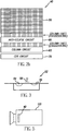
- US Serial No. 10/607,943, filed June 27, 2003 entitled “CMOS Image Sensor Oversaturation Protection Circuit,” by Christina Phan et al., addresses this problem. Referring to Fig. 1 , there is shown a pixel array 10, column and eclipse circuit 20, and a correlated double sampler circuit 30. This prior art technique requires the correction to be implemented in the column and eclipse circuit 20.
- the present invention addresses this shortcoming by permitting the correction to be done as a stand-alone circuit. This preserves the balance of the layout of the column circuit while providing a solution to the eclipse or darkle problem.
- US2003/0179159 discloses a solid state image sensor that includes an imaging circuit, a selection circuit, a signal line and an adjustment circuit.
- the imaging circuit has a plurality of unit cells including a photo-detection section and a first reference potential generating section which generates a first reference potential.
- the selection circuit selects the unit cell.
- the signal line is supplied with a signal potential corresponding to a signal charge from the unit cell in a read-out operation, and supplied with the first reference potential in a reset operation.
- the adjustment circuit operates in response to an adjustment instruction signal which is asserted in an adjustment operation following the reset operation, and applies a second reference potential to the signal line in accordance with a potential of the signal line.
- US2004/0155973 discloses an image sensor of the present invention prevents the phenomenon that surrounding background of a bright object reflecting or emitting strong light like the sun is presented at dark and improves image quality of the image sensor by controlling the brightness of the bright object.
- the image sensor using correlated double sampling technology which outputs data of an object by using difference between a reset voltage signal and a data voltage signal of a unit pixel includes a plurality of unit pixels arranged in a matrix, each outputting the reset voltage signal and the data voltage signal; a plurality of clamping means, each coupled to each unit pixels for clamping up the reset signal to a predetermined voltage level; and a voltage controlling block for adjusting voltage level supplied to a gate of each of clamping means.
- US2004/0119853 discloses an image sensor for capturing an image, having: a plurality of pixels arranged in a matrix each including a photoelectric conversion element for generating current according to received light intensity and a reset transistor for resetting a node of the photoelectric conversion element to a reset potential; and a sample hold circuit for sample holding a pixel potential according to the potential of the node of the pixel.
- the sample hold circuit outputs the differential potential, between a first pixel potential at an end of the integration period after a first reset operation of the pixel and a second pixel potential at an end of a reset noise read period after a second reset operation after the integration period, as a pixel signal. Also in the sample hold circuit, when the second pixel potential during the reset noise read period exceeds a predetermined threshold level, the second pixel potential is set to a predetermined reference potential.
- US6803958 discloses an active pixel sensor (APS) that includes circuitry to eliminate artifacts in digital images.
- the APS includes a comparator for comparing a signal level from a pixel to an adjusted saturation voltage to determine if the pixel is saturated. If the pixel is saturated, the signal output from the pixel is replaced with an analog voltage having a maximum value corresponding to a brightest pixel in the image.
- the present invention provides a CMOS image sensor according to claim 1.
- An advantage of this invention is the preservation of the simplicity and the balance of the layout of the column circuit. This will prevent structure noise from occurring in the image while successfully addressing the eclipse or darkle issue.
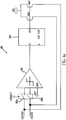
- each pixel 52 includes preferably either a pinned photodiode or a photodiode (sensing region 54) that is exposed to incident light for a desired period of time, referred to as integration, which causes charge to be collected within the sensing region 54.
- the pixel 52 also includes charge-to-voltage conversion circuitry 56 that receives the charge from the sensing region through a transfer gate 58 and converts the charge to a voltage, which will be referenced herein as the sample image signal.
- the operation of the image sensor includes two basic operations, reset and the above-mentioned integration.
- the photodiode is set to a known reference voltage, often referred to as a reset level.
- this reset level is discharged to ground in the integration phase.
- the reset level and the final level after the integration phase sample image signals, are stored in the column circuit 60. These voltages are then subtracted in the correlated double sampler 70.
- an anti-eclipse circuit 80 senses the above-described reset level on the column line and compares it to a preset threshold. If this reset level drops below this threshold, the anti-eclipse circuit 80 will detect and rectify the reset signal level on the column line, as will be described in detail hereinbelow.
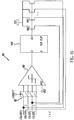
- the anti-eclipse circuit 80 in this description is illustrated as a circuit that provides correction for only 2 columns (coleven, colodd) as shown in Fig 4a .
- coleven is connected to one column and colodd is connected to another column of the pixel array.
- Fig 4b shows that this anti-eclipse circuit can be easily expanded to provide correction for more columns.
- coleveni represents the even columns in the pixel array
- coloddi represents the odd columns, (where i is 1, 2, 3 and the like up to the maximum columns in the pixel array).
- the anti-eclipse circuit 80 is physically separately from the column circuit 60 and shared between multiple columns of pixels for restoring corrupted column voltage on a column of pixels.
- the anti-eclipse circuit 80 is a stand-alone circuit and may be on any side of the pixel array 50.
- Fig. 2b illustrates the anti-eclipse circuit 80 on the same side as the column circuit 60, but is it is still isolated or a stand-alone circuit as noted hereinabove.
- the anti-eclipse or correction circuit 80 includes a comparator 90 that senses the reset signal level on one column line (can be either colodd or coleven) via two electrical connections each in series with a switch 95a and 95b.
- Each switch 95a and 95b is put into a position that permits a connection between the comparator input 90 and column line for permitting the comparator 90 to sense the reset level on the column line only during reset.
- the comparator 90 compares the sensed voltage to a preset threshold. If the voltage on the column line falls below the preset threshold, an eclipse or darkle event is then detected. When this happens, the comparator 90 sends out a trigger signal. The trigger signal is then latched into a digital flip-flop 100 on the rising edge of a signal that also controls reset level sampling on the column circuit 60. The flip-flop 100 will then generate a signal to pull the column line voltage to the level equivalent to the normal (non-eclipse) reset level.
- switches 95a and 95b are put into a position that disconnects the comparator's input from the column line and connects it to ground to deactivate the sensing.
- the column line voltage remains at the corrected level until the clear signal is received by the flip-flop. This "clear" signal is designed to occur after the completion of the sample reset phase of the column circuit 60.
- FIG. 5 there is shown a digital camera or imaging device 110 containing the image sensor 40 of the present invention for illustrating a typical commercial embodiment to which the ordinary consumer is accustomed.
Landscapes
- Engineering & Computer Science (AREA)
- Multimedia (AREA)
- Signal Processing (AREA)
- Transforming Light Signals Into Electric Signals (AREA)
- Solid State Image Pick-Up Elements (AREA)
Applications Claiming Priority (2)
| Application Number | Priority Date | Filing Date | Title |
|---|---|---|---|
| US11/258,812 US7573519B2 (en) | 2005-10-26 | 2005-10-26 | Method for correcting eclipse or darkle |
| PCT/US2006/039786 WO2007050298A1 (en) | 2005-10-26 | 2006-10-12 | Method for correcting eclipse or darkle |
Publications (2)
| Publication Number | Publication Date |
|---|---|
| EP1941716A1 EP1941716A1 (en) | 2008-07-09 |
| EP1941716B1 true EP1941716B1 (en) | 2018-07-04 |
Family
ID=37692665
Family Applications (1)
| Application Number | Title | Priority Date | Filing Date |
|---|---|---|---|
| EP06825786.4A Active EP1941716B1 (en) | 2005-10-26 | 2006-10-12 | Method for correcting eclipse or darkle |
Country Status (6)
| Country | Link |
|---|---|
| US (1) | US7573519B2 (enExample) |
| EP (1) | EP1941716B1 (enExample) |
| JP (1) | JP2009514352A (enExample) |
| KR (1) | KR101289516B1 (enExample) |
| CN (1) | CN101305593B (enExample) |
| WO (1) | WO2007050298A1 (enExample) |
Families Citing this family (19)
| Publication number | Priority date | Publication date | Assignee | Title |
|---|---|---|---|---|
| US7916186B2 (en) | 2005-04-07 | 2011-03-29 | Micron Technology, Inc. | Anti-eclipse circuitry with tracking of floating diffusion reset level |
| KR100834763B1 (ko) * | 2006-11-14 | 2008-06-05 | 삼성전자주식회사 | 동적 촬영 대역의 확장을 위한 이미지 센서 및 화소에수광된 광량을 측정하는 방법 |
| JP5304410B2 (ja) * | 2009-04-17 | 2013-10-02 | ソニー株式会社 | Ad変換装置、固体撮像素子、およびカメラシステム |
| US8310580B2 (en) * | 2009-07-27 | 2012-11-13 | Sony Corporation | Solid-state imaging device and camera system for suppressing occurrence of quantization vertical streaks |
| WO2014018936A2 (en) | 2012-07-26 | 2014-01-30 | Olive Medical Corporation | Continuous video in a light deficient environment |
| CA2878514A1 (en) | 2012-07-26 | 2014-01-30 | Olive Medical Corporation | Ycbcr pulsed illumination scheme in a light deficient environment |
| CA2902319A1 (en) | 2013-02-28 | 2014-09-04 | Olive Medical Corporation | Videostroboscopy of vocal chords with cmos sensors |
| EP2967301B1 (en) | 2013-03-15 | 2021-11-03 | DePuy Synthes Products, Inc. | Scope sensing in a light controlled environment |
| US9777913B2 (en) | 2013-03-15 | 2017-10-03 | DePuy Synthes Products, Inc. | Controlling the integral light energy of a laser pulse |
| CA2906798A1 (en) | 2013-03-15 | 2014-09-18 | Olive Medical Corporation | Super resolution and color motion artifact correction in a pulsed color imaging system |
| US9380232B2 (en) | 2014-02-20 | 2016-06-28 | Semiconductor Components Industries, Llc | Image sensors with anti-eclipse circuitry |
| EP3119265B1 (en) | 2014-03-21 | 2019-09-11 | DePuy Synthes Products, Inc. | Card edge connector for an imaging sensor |
| JP6748622B2 (ja) * | 2017-02-16 | 2020-09-02 | ソニーセミコンダクタソリューションズ株式会社 | 撮像システムおよび撮像装置 |
| US10582138B2 (en) * | 2017-09-22 | 2020-03-03 | Semiconductor Components Industries, Llc | Image sensors with dual conversion gain pixels and anti-eclipse circuitry |
| US10477126B1 (en) | 2018-09-05 | 2019-11-12 | Smartsens Technology (Cayman) Co., Limited | Dual eclipse circuit for reduced image sensor shading |
| US10873716B2 (en) | 2018-11-05 | 2020-12-22 | SmartSens Technology (HK) Co., Ltd. | Dual row control signal circuit for reduced image sensor shading |
| US10727268B1 (en) | 2019-01-25 | 2020-07-28 | Smartsens Technology (Cayman) Co., Ltd | CMOS image sensor with compact pixel layout |
| US10652492B1 (en) | 2019-02-12 | 2020-05-12 | Smartsens Technology (Cayman) Co., Ltd. | CMOS image sensor with improved column data shift readout |
| CN110896082A (zh) | 2019-05-28 | 2020-03-20 | 思特威(上海)电子科技有限公司 | 具有新型布局的图像传感器 |
Citations (3)
| Publication number | Priority date | Publication date | Assignee | Title |
|---|---|---|---|---|
| US20030179159A1 (en) * | 2002-03-01 | 2003-09-25 | Shinji Ohsawa | Solid state image sensor with signal line potential adjustment circuit and method of driving the same |
| US20040119853A1 (en) * | 2002-07-25 | 2004-06-24 | Masatoshi Kokubun | Image sensor providing improved image quality |
| US20040155973A1 (en) * | 2003-01-13 | 2004-08-12 | Chang-Min Bea | Image sensor having clamp circuit |
Family Cites Families (19)
| Publication number | Priority date | Publication date | Assignee | Title |
|---|---|---|---|---|
| US4792859A (en) * | 1987-02-09 | 1988-12-20 | Ovonic Imaging Systems, Inc. | Digitizing wand adapted for manual and automatic operation |
| US6469740B1 (en) * | 1997-02-04 | 2002-10-22 | Matsushita Electric Industrial Co., Ltd. | Physical quantity distribution sensor and method for driving the same |
| JP3517614B2 (ja) * | 1998-12-25 | 2004-04-12 | 株式会社東芝 | 固体撮像装置 |
| US6873363B1 (en) | 1999-02-16 | 2005-03-29 | Micron Technology Inc. | Technique for flagging oversaturated pixels |
| US6803958B1 (en) | 1999-03-09 | 2004-10-12 | Micron Technology, Inc. | Apparatus and method for eliminating artifacts in active pixel sensor (APS) imagers |
| GB0020280D0 (en) * | 2000-08-18 | 2000-10-04 | Vlsi Vision Ltd | Modification of column fixed pattern column noise in solid image sensors |
| US6888572B1 (en) * | 2000-10-26 | 2005-05-03 | Rockwell Science Center, Llc | Compact active pixel with low-noise image formation |
| US6822679B1 (en) * | 2000-10-31 | 2004-11-23 | Texas Instruments Incorporated | Offset correction to the output of a charge coupled device |
| JP2003023570A (ja) * | 2001-07-06 | 2003-01-24 | Sanyo Electric Co Ltd | 画像データの修正方法及び画像信号処理装置 |
| JP3992504B2 (ja) * | 2002-02-04 | 2007-10-17 | 富士通株式会社 | Cmosイメージセンサ |
| JP4251811B2 (ja) * | 2002-02-07 | 2009-04-08 | 富士通マイクロエレクトロニクス株式会社 | 相関二重サンプリング回路とこの相関二重サンプリング回路を備えたcmosイメージセンサ |
| JP4048415B2 (ja) * | 2002-03-13 | 2008-02-20 | ソニー株式会社 | 固体撮像装置及びその駆動方法 |
| JP3912672B2 (ja) * | 2002-07-05 | 2007-05-09 | ソニー株式会社 | 固体撮像装置及びその画素欠陥検査方法 |
| US7502059B2 (en) * | 2002-08-22 | 2009-03-10 | Aptina Imaging Corporation | Asymmetric comparator for use in pixel oversaturation detection |
| JP3862683B2 (ja) * | 2003-07-18 | 2006-12-27 | キヤノン株式会社 | 固体撮像装置 |
| JP4517660B2 (ja) * | 2004-02-09 | 2010-08-04 | ソニー株式会社 | 固体撮像装置、画像入力装置および固体撮像素子の駆動方法 |
| JP2005303746A (ja) * | 2004-04-13 | 2005-10-27 | Matsushita Electric Ind Co Ltd | 撮像装置 |
| US7477298B2 (en) | 2004-08-30 | 2009-01-13 | Micron Technology, Inc. | Anti-eclipsing circuit for image sensors |
| US7659928B2 (en) * | 2005-04-21 | 2010-02-09 | Aptina Imaging Corporation | Apparatus and method for providing anti-eclipse operation for imaging sensors |
-
2005
- 2005-10-26 US US11/258,812 patent/US7573519B2/en active Active
-
2006
- 2006-10-12 CN CN200680040078XA patent/CN101305593B/zh active Active
- 2006-10-12 WO PCT/US2006/039786 patent/WO2007050298A1/en not_active Ceased
- 2006-10-12 KR KR1020087009790A patent/KR101289516B1/ko active Active
- 2006-10-12 EP EP06825786.4A patent/EP1941716B1/en active Active
- 2006-10-12 JP JP2008537744A patent/JP2009514352A/ja active Pending
Patent Citations (3)
| Publication number | Priority date | Publication date | Assignee | Title |
|---|---|---|---|---|
| US20030179159A1 (en) * | 2002-03-01 | 2003-09-25 | Shinji Ohsawa | Solid state image sensor with signal line potential adjustment circuit and method of driving the same |
| US20040119853A1 (en) * | 2002-07-25 | 2004-06-24 | Masatoshi Kokubun | Image sensor providing improved image quality |
| US20040155973A1 (en) * | 2003-01-13 | 2004-08-12 | Chang-Min Bea | Image sensor having clamp circuit |
Also Published As
| Publication number | Publication date |
|---|---|
| EP1941716A1 (en) | 2008-07-09 |
| CN101305593B (zh) | 2010-12-08 |
| US7573519B2 (en) | 2009-08-11 |
| JP2009514352A (ja) | 2009-04-02 |
| KR101289516B1 (ko) | 2013-07-24 |
| CN101305593A (zh) | 2008-11-12 |
| US20070091193A1 (en) | 2007-04-26 |
| KR20080063361A (ko) | 2008-07-03 |
| WO2007050298A1 (en) | 2007-05-03 |
Similar Documents
| Publication | Publication Date | Title |
|---|---|---|
| EP1941716B1 (en) | Method for correcting eclipse or darkle | |
| US20240064412A1 (en) | Method and apparatus providing pixel array having automatic light control pixels and image capture pixels | |
| US8063965B2 (en) | Apparatus and method for eliminating artifacts in active pixel sensor (APS) imagers | |
| EP1887789B1 (en) | Photoelectric conversion device and image capturing device | |
| US8013915B2 (en) | Anti-eclipsing circuit for image sensors | |
| US7081608B2 (en) | Pixel with differential readout | |
| US20030214597A1 (en) | Image sensors including offset adjustment and related methods | |
| US6873363B1 (en) | Technique for flagging oversaturated pixels | |
| US20090190005A1 (en) | Method and apparatus providing pixel-wise noise correction | |
| US10084976B2 (en) | Flux rate unit cell focal plane array | |
| JP2004007394A (ja) | 過飽和減退機能を備えたcmosセンサ | |
| US20040262492A1 (en) | Solid-state image sensing apparatus | |
| US20120249851A1 (en) | Eclipse detection using double reset sampling for column parallel adc | |
| US20060238634A1 (en) | Apparatus and method for providing anti-eclipse operation for imaging sensors | |
| US20090309033A1 (en) | Method and apparatus for reducing temporal row-wise noise in imagers | |
| US8248500B2 (en) | Solid state imaging device | |
| US20060203114A1 (en) | Three-transistor CMOS active pixel | |
| US20060268140A1 (en) | Method and apparatus for reducing noise in analog amplifier circuits and solid state imagers employing such circuits | |
| JP3899176B2 (ja) | 撮像装置 |
Legal Events
| Date | Code | Title | Description |
|---|---|---|---|
| PUAI | Public reference made under article 153(3) epc to a published international application that has entered the european phase |
Free format text: ORIGINAL CODE: 0009012 |
|
| 17P | Request for examination filed |
Effective date: 20080325 |
|
| AK | Designated contracting states |
Kind code of ref document: A1 Designated state(s): DE DK FR GB NL |
|
| DAX | Request for extension of the european patent (deleted) | ||
| RBV | Designated contracting states (corrected) |
Designated state(s): DE DK FR GB NL |
|
| RAP1 | Party data changed (applicant data changed or rights of an application transferred) |
Owner name: OMNIVISION TECHNOLOGIES, INC. |
|
| 17Q | First examination report despatched |
Effective date: 20121220 |
|
| REG | Reference to a national code |
Ref country code: DE Ref legal event code: R079 Ref document number: 602006055767 Country of ref document: DE Free format text: PREVIOUS MAIN CLASS: H04N0003150000 Ipc: H04N0005359000 |
|
| GRAP | Despatch of communication of intention to grant a patent |
Free format text: ORIGINAL CODE: EPIDOSNIGR1 |
|
| INTG | Intention to grant announced |
Effective date: 20180117 |
|
| RIC1 | Information provided on ipc code assigned before grant |
Ipc: H04N 5/359 20110101AFI20180105BHEP |
|
| GRAS | Grant fee paid |
Free format text: ORIGINAL CODE: EPIDOSNIGR3 |
|
| GRAA | (expected) grant |
Free format text: ORIGINAL CODE: 0009210 |
|
| AK | Designated contracting states |
Kind code of ref document: B1 Designated state(s): DE DK FR GB NL |
|
| REG | Reference to a national code |
Ref country code: GB Ref legal event code: FG4D |
|
| REG | Reference to a national code |
Ref country code: DE Ref legal event code: R096 Ref document number: 602006055767 Country of ref document: DE |
|
| REG | Reference to a national code |
Ref country code: NL Ref legal event code: FP |
|
| REG | Reference to a national code |
Ref country code: FR Ref legal event code: PLFP Year of fee payment: 13 |
|
| REG | Reference to a national code |
Ref country code: DE Ref legal event code: R097 Ref document number: 602006055767 Country of ref document: DE |
|
| PLBE | No opposition filed within time limit |
Free format text: ORIGINAL CODE: 0009261 |
|
| STAA | Information on the status of an ep patent application or granted ep patent |
Free format text: STATUS: NO OPPOSITION FILED WITHIN TIME LIMIT |
|
| PG25 | Lapsed in a contracting state [announced via postgrant information from national office to epo] |
Ref country code: DK Free format text: LAPSE BECAUSE OF FAILURE TO SUBMIT A TRANSLATION OF THE DESCRIPTION OR TO PAY THE FEE WITHIN THE PRESCRIBED TIME-LIMIT Effective date: 20180704 |
|
| 26N | No opposition filed |
Effective date: 20190405 |
|
| REG | Reference to a national code |
Ref country code: DE Ref legal event code: R079 Ref document number: 602006055767 Country of ref document: DE Free format text: PREVIOUS MAIN CLASS: H04N0005359000 Ipc: H04N0025620000 |
|
| PGFP | Annual fee paid to national office [announced via postgrant information from national office to epo] |
Ref country code: NL Payment date: 20250916 Year of fee payment: 20 |
|
| PGFP | Annual fee paid to national office [announced via postgrant information from national office to epo] |
Ref country code: GB Payment date: 20250911 Year of fee payment: 20 |
|
| PGFP | Annual fee paid to national office [announced via postgrant information from national office to epo] |
Ref country code: FR Payment date: 20250912 Year of fee payment: 20 |
|
| PGFP | Annual fee paid to national office [announced via postgrant information from national office to epo] |
Ref country code: DE Payment date: 20250912 Year of fee payment: 20 |