EP1938384B1 - Siliziumcarbid-bipolarsperrschichttransistoren mit epitaxialen basisregionen und mehrschicht-emitter und herstellungsverfahren dafür - Google Patents
Siliziumcarbid-bipolarsperrschichttransistoren mit epitaxialen basisregionen und mehrschicht-emitter und herstellungsverfahren dafür Download PDFInfo
- Publication number
- EP1938384B1 EP1938384B1 EP06787147.5A EP06787147A EP1938384B1 EP 1938384 B1 EP1938384 B1 EP 1938384B1 EP 06787147 A EP06787147 A EP 06787147A EP 1938384 B1 EP1938384 B1 EP 1938384B1
- Authority
- EP
- European Patent Office
- Prior art keywords
- sic
- region
- layer
- type
- epitaxial
- Prior art date
- Legal status (The legal status is an assumption and is not a legal conclusion. Google has not performed a legal analysis and makes no representation as to the accuracy of the status listed.)
- Active
Links
Images






Classifications
-
- H—ELECTRICITY
- H10—SEMICONDUCTOR DEVICES; ELECTRIC SOLID-STATE DEVICES NOT OTHERWISE PROVIDED FOR
- H10D—INORGANIC ELECTRIC SEMICONDUCTOR DEVICES
- H10D12/00—Bipolar devices controlled by the field effect, e.g. insulated-gate bipolar transistors [IGBT]
- H10D12/01—Manufacture or treatment
- H10D12/031—Manufacture or treatment of IGBTs
-
- H—ELECTRICITY
- H10—SEMICONDUCTOR DEVICES; ELECTRIC SOLID-STATE DEVICES NOT OTHERWISE PROVIDED FOR
- H10D—INORGANIC ELECTRIC SEMICONDUCTOR DEVICES
- H10D10/00—Bipolar junction transistors [BJT]
- H10D10/40—Vertical BJTs
-
- H—ELECTRICITY
- H10—SEMICONDUCTOR DEVICES; ELECTRIC SOLID-STATE DEVICES NOT OTHERWISE PROVIDED FOR
- H10D—INORGANIC ELECTRIC SEMICONDUCTOR DEVICES
- H10D10/00—Bipolar junction transistors [BJT]
- H10D10/01—Manufacture or treatment
- H10D10/051—Manufacture or treatment of vertical BJTs
-
- H—ELECTRICITY
- H10—SEMICONDUCTOR DEVICES; ELECTRIC SOLID-STATE DEVICES NOT OTHERWISE PROVIDED FOR
- H10D—INORGANIC ELECTRIC SEMICONDUCTOR DEVICES
- H10D62/00—Semiconductor bodies, or regions thereof, of devices having potential barriers
- H10D62/10—Shapes, relative sizes or dispositions of the regions of the semiconductor bodies; Shapes of the semiconductor bodies
- H10D62/13—Semiconductor regions connected to electrodes carrying current to be rectified, amplified or switched, e.g. source or drain regions
- H10D62/133—Emitter regions of BJTs
-
- H—ELECTRICITY
- H10—SEMICONDUCTOR DEVICES; ELECTRIC SOLID-STATE DEVICES NOT OTHERWISE PROVIDED FOR
- H10D—INORGANIC ELECTRIC SEMICONDUCTOR DEVICES
- H10D62/00—Semiconductor bodies, or regions thereof, of devices having potential barriers
- H10D62/10—Shapes, relative sizes or dispositions of the regions of the semiconductor bodies; Shapes of the semiconductor bodies
- H10D62/17—Semiconductor regions connected to electrodes not carrying current to be rectified, amplified or switched, e.g. channel regions
- H10D62/177—Base regions of bipolar transistors, e.g. BJTs or IGBTs
-
- H—ELECTRICITY
- H10—SEMICONDUCTOR DEVICES; ELECTRIC SOLID-STATE DEVICES NOT OTHERWISE PROVIDED FOR
- H10D—INORGANIC ELECTRIC SEMICONDUCTOR DEVICES
- H10D62/00—Semiconductor bodies, or regions thereof, of devices having potential barriers
- H10D62/80—Semiconductor bodies, or regions thereof, of devices having potential barriers characterised by the materials
- H10D62/83—Semiconductor bodies, or regions thereof, of devices having potential barriers characterised by the materials being Group IV materials, e.g. B-doped Si or undoped Ge
- H10D62/832—Semiconductor bodies, or regions thereof, of devices having potential barriers characterised by the materials being Group IV materials, e.g. B-doped Si or undoped Ge being Group IV materials comprising two or more elements, e.g. SiGe
- H10D62/8325—Silicon carbide
Definitions
- This invention relates to power semiconductor devices and related methods of fabricating power semiconductor devices and, more particularly, to high voltage silicon carbide devices and related methods of fabricating high voltage silicon carbide devices.
- BJT bipolar junction transistor
- the material that makes up a device contributes to the operability and usefulness of the device.
- conventional BJTs are typically formed of silicon (Si), but can also include gallium arsenide (GaAs) and indium phosphide (InP).
- silicon carbide (SiC) has been used as a material for BJTs.
- SiC has advantageous semiconductor characteristics, for example, a wide bandgap, high electric field breakdown strength, high electron mobility, high thermal conductivity, high melting point, and high saturated electron drift velocity.
- electronic devices formed in SiC may have the capability of operating at higher temperatures, at high power densities, at higher speeds, at higher power levels and even under high radiation densities.
- SiC transistors Due to their ability to function at high frequencies, high temperatures, and high power levels, SiC transistors are highly desirable for use in applications such as high frequency transmitters for radar and communications, for high power switching applications, and for high temperature operations such as jet engine control. Accordingly, methods of producing device quality SiC and devices formed from SiC have been of interest to scientists and engineers for several decades.
- SiC crystallizes in over 150 different polytypes, or crystal structures, of which the most common are designated 3C, 4H, and 6H where "C” stands for "cubic” and “H” for "hexagonal.”
- SiC is a difficult material to use in semiconductor devices.
- the high melting point of SiC may render techniques, such as alloying and diffusion of dopants, more difficult, usually because a number of the other materials necessary to perform such operations tend to break down at the high temperatures used to affect SiC.
- SiC is also an extremely hard material, and indeed its most common use is as an abrasive. Attempts have been made, with some success, in manufacturing junctions, diodes, transistors, and other devices from SiC.
- SiC BJTs are discussed in, for example, United States Patent No. 4,945,394 to Palmour et al. , the disclosure of which is incorporated herein by reference as if set forth in its entirety. As discussed therein, SiC BJTs are formed having a base and an emitter formed as wells using high temperature ion implantation. Furthermore, SiC BJTs are also discussed in United States Patent No. 6,218,254 to Singh et al ., the content of which is incorporated herein by reference as if set forth in its entirety. As discussed therein, SiC BJTs having a base and an emitter are formed using epitaxial growth and high temperature ion implantation. Singh further discusses the use of removable dielectric spacers to improve the alignment of base and emitter regions. '
- SiC BJTs typically include at least one highly doped implant region for the base or the emitter.
- the formation of the implant region may cause damage to the SiC crystal.
- the current gain of the device may be reduced due to surface recombination current due to implant induced defects.
- the current gain of the device may be reduced as a function of time due to stacking faults in the base region, which may result from the defects created by the implantation process.
- the highly doped emitter regions present in these devices may have a poor lifetime, which may further reduce the current gain of the device.
- an N- SiC layer 11 is provided on a highly doped N + SiC substrate 10.
- a p-type (P) SiC layer 12 is provided on the NSiC layer 11.
- n-type emitter regions 20 (N + ) and highly doped p-type base regions 25 (P + ) are provided on the p-type layer 12.
- the emitter regions 20 may be formed by epitaxial growth and subsequent etching and base regions 25 may be formed by implantation techniques.
- the implantation of the P + base regions 25 may be carried out at from about 650°C to about 1100°C using aluminum ions (Al + ) having energy ranging from about 20 keV to about 360 keV.
- Al + aluminum ions
- this implant may cause damage to the SiC crystal, which may not be entirely removed by a high temperature (1600-1700 °C) activation anneal.
- the defects introduced by the implant may result in surface recombination current and stacking fault formation in the base region of the device.
- a passivation layer 18 is provided on the surface of the device.
- the BJT further includes an ohmic metal 30/31 and an overlayer metal 16 that provide contacts to the base (B) regions 25, the emitter (E) regions 20 and the collector (C) regions 10/11.
- the highly doped regions designated as N + 20, 10 and P + 25 may be provided to improve the quality of the ohmic contacts.
- Embodiments of the present invention provide bipolar junction transistors (BJTs) including silicon carbide (SiC) substrates.
- An epitaxial SiC base region is provided on the SiC substrate.
- the eptiaxial SiC base region has a p- conductivity type.
- An epitaxial SiC emitter region is also provided on the SiC substrate.
- the epitaxial SiC emitter region has a n- conductivity type, from the first conductivity type.
- the epitaxial SiC emitter region has first and second portions. The first portion is provided on the SiC substrate and the second portion is provided on the first portion remote from the SiC substrate. The second portion has a higher carrier concentration than the first portion.
- the epitaxial SiC base region includes a first p-type epitaxial SiC layer on the SiC substrate.
- a first p-type epitaxial SiC region is provided on the first p-type epitaxial SiC layer.
- the first p-type epitaxial SiC region has a higher carrier concentration than the first p-type epitaxial SiC layer.
- a second p-type epitaxial SiC region is provided on the first p-type epitaxial SiC region, remote from the first p-type epitaxial SiC layer.
- the second p-type epitaxial SiC region has a higher carrier concentration than the first p-type epitaxial SiC region.
- the first p-type epitaxial SiC layer may have a carrier concentration of from about 1.0 X 10 16 cm -3 to about 1.0 X 10 19 cm -3 and a thickness of from about 0.1 ⁇ m to about 10 ⁇ m.
- the first p-type epitaxial SiC region may have a carrier concentration of from about 1.0 X 10 18 cm -3 to about 1.0 X 10 19 cm -3 and a thickness of from about 0.1 ⁇ m to about 10 ⁇ m.
- the second p-type epitaxial SiC region may have a carrier concentration of from about 1.0 X 10 19 cm -3 to about 5 x 10 20 cm -3 and a thickness of from about 0.1 ⁇ m to about 3.0 ⁇ m.
- the epitaxial SiC base region may include a first p-type epitaxial SiC layer on the SiC substrate and a p-type epitaxial SiC region on the first p-type epitaxial SiC layer, remote from the SiC substrate.
- the p-type epitaxial SiC region may have a higher carrier concentration than the first p-type epitaxial SiC layer.
- the first p-type epitaxial SiC layer may have a carrier concentration of from about 1.0 X 10 16 cm -3 to about 1.0 X 10 19 cm -3 and a thickness of from about 0.1 ⁇ m to about 10 ⁇ m.
- the p-type epitaxial SiC region may have a carrier concentration of from about 1.0 X 10 18 cm -3 to about 5 x 10 20 cm -3 and a thickness of from about 0.1 ⁇ m to about 10 ⁇ m.
- the first portion of the epitaxial SiC emitter region may include n-type SiC having a carrier concentration of from about 1.0 X 10 17 cm -3 to about 5 x 10 19 cm -3 and may have a thickness of from about 0.1 ⁇ m to about 5 ⁇ m.
- the second portion of the epitaxial SiC emitter region may include n-type SiC having a carrier concentration of from about 5 x 10 18 cm -3 to about 5 x 10 20 cm -3 and may have a thickness of from about 0.1 ⁇ m to about 3.0 ⁇ m.
- a first layer of SiC having the second conductivity type may be provided on the SiC substrate between the SiC substrate and the epitaxial SiC base region.
- a second layer of SiC having the first conductivity type may be provided on the first layer of SiC.
- the epitaxial SiC base region and the epitaxial SiC emitter region may be on the second layer of SiC, remote from the first layer of SiC.
- the first conductivity type may be p-type conductivity SiC and the second conductivity type may be n-type conductivity SiC.
- the first layer of SiC may have a carrier concentration of from about 1.0 X 10 13 cm -3 to about 1.0 X 10 17 cm -3 and a thickness of from about 1.0 ⁇ m to about 250 ⁇ m.
- Still further embodiments of the present invention provide BJTs having a silicon carbide (SiC) substrate and an epitaxial SiC emitter region on the SiC substrate.
- the epitaxial SiC emitter region has a n-conductivity type.
- the epitaxial SiC emitter region has first and second portions. The first portion is provided on the SiC substrate and the second portion is provided on the first portion, remote from the SiC substrate. The second portion has a higher carrier concentration than the first portion.
- Embodiments of the present invention are described herein with reference to cross-section illustrations that are schematic illustrations of idealized embodiments of the present invention. As such, variations from the shapes of the illustrations as a result, for example, of manufacturing techniques and/or tolerances, are to be expected. Thus, embodiments of the present invention should not be construed as limited to the particular shapes of regions illustrated herein but are to include deviations in shapes that result, for example, from manufacturing. For example, an implanted region illustrated as a rectangle will, typically, have rounded or curved features and/or a gradient of implant concentration at its edges rather than a binary change from implanted to non-implanted region.
- a buried region formed by implantation may result in some implantation in the region between the buried region and the surface through which the implantation takes place.
- the regions illustrated in the figures are schematic in nature and their shapes are not intended to illustrate the precise shape of a region of a device and are not intended to limit the scope of the present invention.
- doped regions of silicon carbide may be formed through epitaxial growth and/or through implantation.
- a p-type region of silicon carbide may be formed through epitaxial growth in the presence of a p-type dopant or through implantation of p-type dopants in an undoped, p-type or n-type epitaxial layer.
- the structure that results from epitaxial growth differs from that that results from implantation.
- the terms "epitaxial region” and "implanted region” structurally distinguish differing regions of silicon carbide and may be used herein as a recitation of structural characteristics of the regions of silicon carbide and/or as recitations of methods of forming such regions of silicon carbide.
- the embodiments of the present invention provide bipolar junction transistors (BJTs) having epitaxial silicon carbide (SiC) base regions and multilayer epitaxial emitter regions.
- BJTs bipolar junction transistors
- SiC silicon carbide
- the use of an epitaxial SiC base region in BJTs according to some embodiments of the present invention may eliminate the need for implantation and a subsequent high temperature anneal, which may cause damage to the SiC crystal and, thereby, cause a reduction in the current gain of the device. Accordingly, BJTs according to the embodiments of the present invention may have improved current gains relative to conventional devices.
- the use of a multilayer epitaxial SiC emitter region may allow the current gain of the device to be further increased as discussed further herein with respect to Figures 2 through 16 .
- SiC BJTs may offer the potential of operating reliably at much higher junction temperatures as compared to, for example, SiC MOSFETs.
- the overall losses (switching and conduction) of the SiC BJT operating at, for example, 250°C are approximately from about 50 to about 60 percent lower than the comparable Si Insulated Gate Bipolar Transistor (IGBT) operating at 25°C.
- IGBT Insulated Gate Bipolar Transistor
- the combination of higher junction temperature and reduced losses may result in a sufficient reduction of cooling requirements to warrant a more complicated gate drive circuit used to operate BJTs.
- Si IGBTs operate with junction temperatures in the range of from about 115 to about 125°C, dangerously close to the maximum allowable junction temperature for Si IGBTs.
- SiC BJTs may be capable of operating at higher junction temperatures and, therefore, may not malfunction as discussed above as will be discussed further herein.
- a silicon carbide (SiC) substrate 100 may be provided.
- the polarity of the substrate 100 may be n-type or p-type SiC having a polytype of, for example, 3C, 2H, 4H, 6H or 15R.
- Devices discussed according the present invention illustrated in Figure 2 include n-type SiC substrates 100.
- the substrate 100 is a highly doped n-type SiC (N + ).
- N + n-type SiC
- the substrate 100 may be doped with n-type dopants, such as nitrogen.
- the substrate may have a carrier concentration of from about 1.0 X 10 18 cm -3 to about 5.0 X 10 19 cm -3 and a thickness of from about 200 ⁇ m to about 500 ⁇ m.
- a first epitaxial layer 101 is provided on a first side 100A of the SiC substrate 100.
- the first epitaxial layer 101 may be doped with n-type dopants, such as nitrogen.
- the first epitaxial layer 101 may have a carrier concentration of from about 1.0 X 10 13 cm -3 to about 1.0 X 10 17 cm -3 and a thickness of from about 1.0 ⁇ m to about 250 ⁇ m.
- the substrate 100 and the first epitaxial layer 101 define the collector (C) region of the BJT.
- a second epitaxial layer 102 is provided on the first epitaxial layer 101 and may be doped with p-type dopants, such as aluminum or boron.
- the second epitaxial layer 102 may have a carrier concentration of from about 1.0 X 10 16 cm -3 to about 1.0 X 10 19 cm -3 and a thickness of from about 0.1 ⁇ m to about 10 ⁇ m.
- An epitaxial SiC base contact region 140 is provided on the second epitaxial layer 102. As illustrated in Figure 2 , the epitaxial SiC base contact region 140 includes a first p-type epitaxial SiC region 113 on the second epitaxial layer and a second p-type epitaxial SiC region 103 on the first p-type epitaxial SiC region 113.
- the first p-type epitaxial SiC region 113 has a carrier concentration of from about 1.0 X 10 18 cm -3 to about 1.0 X 10 19 cm -3 and a thickness of from about 0.1 ⁇ m to about 10 ⁇ m.
- the second p-type epitaxial SiC region 103 has a carrier concentration of from about 1.0 X 10 19 cm -3 to about 5.0 X 10 20 cm -3 and a thickness of from about 0.1 ⁇ m to about 3.0 ⁇ m.
- the second epitaxial base layer 102 and the epitaxial SiC base contact region (first and second p-type epitaxial SiC regions 113 and 103) form the base (B) region of the BJT according to some embodiments of the present invention.
- the SiC base contact region is epitaxially grown, which may eliminate the need for implantation and high temperature anneals that may damage the SiC crystal. Accordingly, devices according to the present invention may have higher current gains as discussed further herein.
- an epitaxial SiC emitter region 145 is provided on the second epitaxial layer 102.
- the epitaxial SiC emitter region 145 has an n-type conductivity.
- the epitaxial SiC emitter region 145 has first (N) and second (N + ) portions 104 and 105, respectively.
- the first portion 104 of the epitaxial SiC emitter region is provided on the second epitaxial layer 102 and is doped with n-type dopants, such as nitrogen.
- the first portion 104 of the epitaxial SiC emitter region has a carrier concentration of from about 1.0 X 10 17 cm -3 to about 5 X 10 19 cm -3 and a thickness of from about 0.1 ⁇ m to about 5.0 ⁇ m.
- the second portion 105 of the epitaxial SiC emitter region is doped with n-type dopants, such as nitrogen, and has a higher carrier concentration relative to the first portion 104.
- the second portion 105 of the epitaxial SiC emitter region has a carrier concentration of from about 5 X 10 18 cm -3 to about 5 X 10 20 cm -3 and a thickness of from about 0.1 ⁇ m to about 3.0 ⁇ m.
- the epitaxial SiC emitter region 145 includes a low-doped n-type layer 104 that may provide improved injection efficiency and a highly doped n-type layer 105 that may provide an improved contact surface.
- a passivation layer 108 is provided on the second epitaxial layer 102, the epitaxial SiC base region 140 and the epitaxial SiC emitter region 145.
- the passivation layer 108 may include, for example, thermally grown silicon dioxide (SiO 2 ), chemical vapor deposited SiO 2 and/or chemical vapor deposited silicon nitride (Si 3 N 4 ).
- Ohmic metal 130 suitable for n-type silicon carbide, is provided on the second portion 105 of the epitaxial SiC emitter region 145 for emitter fabrication. The ohmic metals are annealed to provided ohmic contacts as discussed further below.
- Some embodiments of the present invention include conductive substrates 100.
- ohmic metal 130 is also provided on a second side 100B of substrate 100 for collector fabrication. It will be understood by those skilled in the art that the present invention could be implemented using a non-conducting substrate, such as semi-insulating silicon carbide or sapphire, in which case the ohmic metal 130 for collector formation would be provided on a surface of the first SiC layer 101.
- Ohmic metal 131 suitable for p-type silicon carbide, is provided on the second SiC p-type region 103 for base fabrication.
- Metals and/or metal composites may be appropriate for the ohmic contacts 130 and 131.
- nickel or nickel-titanium combinations are appropriate ohmic contacts 130 to n-type silicon carbide while aluminum or aluminum-titanium combinations are appropriate ohmic contacts 131 to p-type silicon carbide.
- cobalt silicide CoSi 2
- Ohmic contacts are discussed in United States Patent Nos.
- An overlayer metal 106 such as gold, may be deposited on the ohmic contacts 130 and 131 as illustrated in Figure 2 .
- the substrate 100 may have a polytype of, for example, 3C, 2H, 4H, 6H or 15R.
- the substrate 100 may be doped during the growth phase with a donor dopant, such as nitrogen, at a concentration from about 1.0 X 18 18 cm -3 to about 5 X 10 19 cm -3 .
- the substrate 100 may also have a thickness of from about 200 ⁇ m to about 500 ⁇ m.
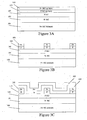
- a first epitaxial layer 101, having n-type conductivity (N) is formed on the substrate 100.
- the first epitaxial layer 101 is doped with a donor dopant, such as nitrogen, at a concentration of from about 1.0 X 10 13 cm -3 to about 1.0 X 10 17 cm -3 .
- the first epitaxial layer 101 has a thickness of from about 1.0 ⁇ m to about 250 ⁇ m.
- the substrate 100 and the first epitaxial layer 101 define the collector region of the BJT according to the present invention.
- a second epitaxial layer 102 having p-type (P) conductivity is formed on first epitaxial layer 101.
- the second epitaxial layer 102 is doped with an acceptor dopant, such as aluminum or boron, at a concentration of from about 1.0 X 10 16 cm -3 to about 1.0 X 10 19 cm -3 .
- the second epitaxial layer 102 has a thickness of from about 0.1 ⁇ m to about 10 ⁇ m.
- a third epitaxial layer 113 having p-type conductivity is formed on the second epitaxial layer 102.
- the third epitaxial layer 113 is more highly doped than the second epitaxial layer 102.
- the third epitaxial layer 113 is doped with an acceptor dopant, such as aluminum or boron, at a carrier concentration of from about 1.0 X 10 18 cm -3 to about 1.0 X 10 19 cm -3 .
- the third epitaxial layer 113 has a thickness of from about 0.1 ⁇ m to about 10 ⁇ m.
- a fourth epitaxial layer 103 is formed on the third epitaxial layer 113 and is more highly doped than the third epitaxial layer.
- the fourth epitaxial layer 103 is doped with an acceptor dopant, such as aluminum or boron, at a concentration of from about 1.0 X 10 19 cm -3 to about 5 X 10 20 cm -3 .
- the fourth epitaxial layer 103 has a thickness of from about 0.1 ⁇ m to about 3.0 ⁇ m.
- regions of the third and fourth epitaxial layers 113 and 103 are isolated as mesas on the surface of the second epitaxial layer 102 using, for example, photolithographic techniques such as a patterned photoresist and subsequent etching to provide first and second p-type epitaxial SiC regions 113 and 103 of an epitaxial SiC base region (140 Figure 2 ).
- reactive ion etching of epitaxial layers may be implemented to define mesas for base and emitter contacts.
- the epitaxial layers may be etched using reactive ion etching with nitrogen trifluoride (NF 3 ). NF 3 has demonstrated a number of advantages in silicon carbide etching processes.
- Reactive ion etching using NF 3 is discussed Surface Characteristics of Monocrystalline Beta-SiC Dry Etched in Fluorinated Gases by Palmour et al. (Mat. Res. Soc. Symp. Proc., Vol. 76, 1987, p. 185 ), the disclosure of which is incorporated herein by reference as if set forth in its entirety. Techniques for etching silicon carbide are also discussed in United States Patent Nos. 4,865,685 and 4,981,551 to Palmour , the disclosures of which are incorporated herein by reference as if set forth in their entirety.
- the third and fourth epitaxial layers 113 and 103 may be etched until at least a portion the surface of the second epitaxial layer 102 is exposed.
- some embodiments of the present invention provide a 0.4 ⁇ m mesa of third and fourth epitaxial layers 113 and 103.
- an electrical check from front to back may determine when the etching process should be terminated. This step may then be followed by an overetch, for example, a 15 percent overetch.
- the second epitaxial layer 102 and the epitaxial SiC base region 140 including the first p-type epitaxial SiC region 113 and the second p-type epitaxial SiC region 103 may define the base region of the BJT according to some embodiments of the present invention.
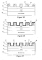
- a fifth epitaxial layer 104 of n-type conductivity may be re-grown on the surface of the second epitaxial layer 102 and the first and second p-type epitaxial SiC regions 113 and 103.
- the fifth epitaxial layer 104 is doped with a donor dopant, such as nitrogen, at a concentration of from about 1.0 X 10 17 cm -3 to about 5 X 10 19 cm -3 .
- the fifth epitaxial layer 104 has a thickness of from about 0.1 ⁇ m to about 5 ⁇ m.
- a sixth epitaxial layer 105, having a higher carrier concentration relative to the fifth epitaxial layer 104, is grown on the fifth epitaxial layer 104.
- the sixth epitaxial layer 105 is doped with a donor dopant, such as nitrogen, at a concentration of from about 5 X 10 18 cm -3 to about 5 X 10 20 cm -3 .
- the sixth epitaxial layer 105 has a thickness of from about 0.1 ⁇ m to about 3 ⁇ m.
- regions of the fifth and sixth epitaxial layers 104 and 105 are isolated as mesas on the surface of the second epitaxial layer 102 using, for example, a patterned photoresist and subsequent etching as discussed with respect to Figure 3B to provide first and second portions 104 and 105 of an epitaxial SiC emitter region (145 Figure 2 ).
- the fifth and sixth epitaxial layers 104 and 105 are etched until at least a portion of the surface of the second epitaxial layer 102 is exposed.
- the first and second portions 104 and 105 define the emitter region of the BJT according to some embodiments of the present invention.
- a passivation layer 108 is formed on the surface of the second epitaxial layer 102, the first and second p-type epitaxial SiC regions 113 and 103 and the first and second portions 104 and 105 of the emitter region.
- the passivation layer 108 may include, for example, thermally grown SiO 2 , chemical vapor deposited SiO 2 and/or chemical vapor deposited Si 3 N 4 .
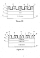
- windows 120 may be opened in the passivation layer 108 by, for example, selectively etching the passivation layer 108. The passivation is etched until at least a portion of the surface of the second portion 105 of the emitter region is exposed.
- ohmic metal 130 suitable for n-type silicon carbide, is deposited on the exposed surfaces of the second portion 105 of the emitter region for emitter fabrication.
- the ohmic metals may be deposited using, for example, e-beam evaporation and the ohmic metals may be annealed at high temperatures, for example, temperatures from about 625°C to about 1000°C to
- windows 121 may be opened in the passivation layer 108 by, for example, selectively etching the passivation layer 108.
- the passivation layer 108 may be etched until at least a portion of the surface of the second p-type epitaxial SiC region 103 is exposed.
- ohmic metal 131 suitable for p-type silicon carbide, is deposited on exposed surfaces of the second p-type epitaxial SiC region 103 for base fabrication.
- BJTs according to some embodiments of the present invention are illustrated in, for example, Figure 3J .
- an overlayer metal 106 such as gold, may be formed on the ohmic contacts 130 and 131.
- FIG. 5A processing steps in the fabrication of the substrate 100, first epitaxial layer 101 and second epitaxial layer 102 are similar to the processing steps of like numbered elements discussed with respect to Figure 3A and, therefore, details with respect to the processing steps of these elements will not be repeated herein.
- a third epitaxial layer 504 having an n-type conductivity is grown on the second epitaxial layer 103.
- a fourth epitaxial layer 505, having higher n-type conductivity relative to the third epitaxial layer 504, is grown on the third epitaxial layer 504.
- the third and fourth epitaxial layers 504 and 505 define an emitter region of the BJT.
- regions of the third and fourth epitaxial layers 504 and 505 are isolated on the surface of the second epitaxial layer 102 using, for example, photolithographic techniques as a patterned photoresist and subsequent etching.
- the third and fourth epitaxial layers 504 and 505 are etched until at least a portion of the second epitaxial layer 102 is exposed.
- fifth and sixth epitaxial layers 513 and 503 of p-type conductivity are re-grown on the surface of the second epitaxial layer 102 and the first and second portions 504 and 505 of the emitter region.
- the sixth epitaxial layer 503 is more highly doped relative to the fifth epitaxial layer 513.
- the fifth epitaxial layer 513 is more highly doped than the second epitaxial layer 102.
- the device illustrated in Figure 5C is etched to isolate regions of epitaxial layers 513 and 503.
- the fifth and sixth epitaxial layers 513 and 503 are etched until at least a portion of the surface of second epitaxial layer 102 is exposed.
- the second epitaxial layer 102 and isolated layers 513 and 503 define the base region of the BJT ( Figure 3D ).
- FIGs 5A through 5C illustrate that the emitter portions 504 and 505 may be formed before the first and second layers 513 and 503 of the base region without departing from the scope of the present invention. Processing steps in the fabrication of the remaining portions of the BJT according to some embodiments of the present invention are similar to those discussed above with respect to Figures 3E-3J and, therefore, will not be repeated herein.
- FIG. 6A the processing steps in the fabrication of the substrate 100, first epitaxial layer 101, the second epitaxial layer 102, the first SiC region 113 and the second SiC region 103 are similar to processing steps of the like numbered elements discussed with respect to Figure 3A and, therefore, details with respect to the processing steps of these elements will not be repeated herein.
- a masking layer 640 is deposited on the surface of the second epitaxial layer 102 and the first and second regions of SiC 113 and 103.
- the masking layer 640 may include, for example, SiO 2 , Si 3 N 4 , tantalum carbide (TaC), or any other similar material capable of withstanding an epitaxial growth temperature of about 1600 °C for about 30 minutes and can subsequently be removed.
- window 641 are formed in masking layer 640 by, for example, selective etching.
- a first epitaxial layer 604 having n-type conductivity and a second epitaxial layer 605 having a higher n-type conductivity relative to the first epitaxial layer 604 are formed in the windows 641 to form the emitter region of the BJT.
- the remaining masking layer 640 is removed to provide an intermediate device similar to the device illustrated in Figure 3D . Processing steps in the fabrication of the remaining portions of the BJT according to some embodiments of the present invention are similar to those discussed above with respect to Figures 3E-3J and, therefore, will not be repeated herein.
- a masking layer 750 is provided on the surface of the second epitaxial layer 102 and the first and second portions 704 and 705.
- the masking layer 750 may include, for example, silicon dioxide (SiO 2 ), TaC, and the like.
- windows 742 may be opened in masking layer 750 by, for example, selective etching.
- epitaxial layers 713 and 703 having p-type conductivities are formed in the windows 742 and together with layer 102 form the base region of the BJT.
- the remaining masking layer 750 is removed to provide an intermediate device similar to the device illustrated in Figure 3D .
- Figures 7A through 7C are provided to illustrate that either the emitter region or the base region of the BJT may be formed using the processes discussed in Figures 6A through 6C and 7A through 7C . Processing steps in the fabrication of the remaining portions of the BJT according to some embodiments of the present invention are similar to those discussed above with respect to Figures 3E-3J and, therefore, will not be repeated herein.
- NPN BJTs were tested for stability.
- NPN BJTs were fabricated in 4H-SiC with a 14 ⁇ m thick n-type collector layer doped at 4.8 x 10 15 cm -3 , a 1.0 ⁇ m thick p-type base layer doped at 2x10 17 cm -3 and 2.0 ⁇ m thick n-type emitter layer doped at 3.0 x 10 19 cm -3 .
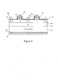
- a simplified BJT structure is illustrated a cross section of the 4H-SiC BJT of Figure 9 which is not part of the invention.
- the device of Figure 9 has a pitch of 25.0 ⁇ m.
- the chip size is 1.88 mm x 1.88 mm with a total emitter width of 62 mm and an active area of 0.0225 cm 2 , as illustrated in the plan view of the SiC BJT of Figure 10 .
- the details with respect to the fabrication of such devices are discussed in, for example, ISPSD Proceedings (2005), p. 271 by Agarwal et al. and IEEE Electron Device Letters Vol. 26, No. 3 (2005), p. 175 by Krishnaswami et al., the disclosures of which are hereby incorporated herein by reference as if set forth in their entirety.
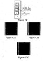
- the DC output characteristics of one of the devices in common emitter mode are illustrated in Figures 11A through 11D , before and after many hours of stress at a collector current of 10A.
- a SiC BJT having the conventional structure shown in Figure 1 was operated at 10.0 A over various time intervals, i.e., 0 minutes (Figure 9A), 15 minutes (Figure 9B), 30 minutes (Figure 9C) and 16 hours ( Figure 9D).
- the device was packaged in a metal package. After the initial measurement, the device was stressed at 10 A for a given amounts of time. The device was powered down, allowed to cool and then the output characteristics were recorded.
- both the current gain and the on-resistance may be reduced over time. Accordingly, conventional SiC BJTs show instability in the I-V characteristics after as little as 15 minutes of operation.
- the dislocations created by the p + implant 25 of the conventional BJT of Figure 1 may be responsible for the deterioration of the device characteristics.
- Stacking fault growth within the base layer may be observed by light emission imaging.
- the energy for this expansion of the stacking fault may come from the electron-hole recombination in the forward biased base-emitter junction. This may result in reduction of the effective minority carrier lifetime, increasing the electron-hole recombination in the base in the immediate vicinity of the stacking fault, which may lead to a reduction in the current gain.
- SiC BJTs the reduction in the current gain of SiC BJTs may be explained based on what has been previously observed in SiC pn junction diodes. Details with respect to SiC junction diodes are discussed in, for example, Material Science. Forum Vol. 353-356 (2001), p. 727 by Lendenmann et al ., Applied Physics. Letters 81 (2002), p. 883 by Galeckas et al. and Material Science Forum Vol. 457-460 (2004), p. 1113 by Sumakeris et al., the disclosures of which are hereby incorporated herein by reference as if set forth in their entirety.
- V f forward voltage
- This V f increase was explained by the growth of stacking faults from certain basal plane dislocations within the drift layer of the PiN diode.
- the energy for this expansion of the stacking fault comes from the electron-hole recombination in the conductivity modulated drift layer.
- This may result in reduction of the minority carrier lifetime, reducing the conductivity modulation in the immediate vicinity of the stacking fault, leading to an increase in V f .
- a similar phenomenon may be taking place in the SiC BJT device.
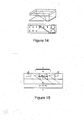
- the base of the transistor is flooded with electron-hole pairs during operation as illustrated in, for example, Figure 14 .
- the recombination of electron-hole pairs in the base may give rise to stacking faults as pictorially illustrate in Figure 15 .
- These stacking faults may reduce the lifetime of the minority carriers locally in the base, which in turn may result in reduced current gain.
- the reduction in current gain may also explain the increase in the on-resistance of the BJT in the saturation region since not many carriers make it across the base into the collector.
- the increase in the slope of the I-V curves in the linear region indicates that the base doping has been effectively reduced, resulting in an enhanced "Early Effect.” This could also be the consequence of the generated stacking faults in the base.
- Figure 16 illustrates exemplary I-V characteristics obtained with the structure shown in Figure 16 according to some embodiments of the present invention.
- Four traces of the output characteristics of a SiC BJT according to some embodiments of the present invention with increasing stress exhibits relatively small drift in current gain. Accordingly, the current gain drift and the reduction in the on-resistance may be suppressed according to some embodiments of the present invention.
Landscapes
- Bipolar Transistors (AREA)
- Electrodes Of Semiconductors (AREA)
Claims (8)
- Bipolarer Sperrschichttransistor (BST), mit:einem Substrat (100) aus Siliziumkarbid (SiC);einem p-leitenden Basisbereich (B) auf dem SiC-Substrat, wobei der Basisbereich eine p-leitende epitaxiale SiC-Schicht (102) auf dem SiC-Substrat und einen epitaxialen SiC-Basisbereich (140) auf der p-leitenden epitaxialen SiC-Schicht aufweist; undeinen n-leitenden epitaxialen SiC-Emitterbereich (145) auf der p-leitenden epitaxialen SiC-Schicht, der von dem epitaxialen SiC-Basisbereich beabstandet ist, wobei der epitaxiale SiC-Emitterbereich einen ersten n-leitenden epitaxialen SiC-Bereich (104) auf der p-leitenden epitaxialen SiC-Schicht und einen zweiten n-leitenden epitaxialen SiC-Bereich (105) auf dem ersten n-leitenden epitaxialen SiC-Bereich aufweist, wobei der zweite n-lei-tende epitaxiale SiC-Bereich eine höhere Trägerkonzentration aufweist als der erste n-lei-tende epitaxiale SiC-Bereich; unddadurch gekennzeichnet, dass der epitaxiale SiC-Basisbereich Folgendes aufweist:einen ersten p-leitenden epitaxialen SiC-Bereich (113) auf der p-leitenden epitaxialen SiC-Schicht, wobei der erste p-leitende epitaxiale SiC-Bereich eine höhere Trägerkonzentration aufweist als die p-leitende epitaxiale SiC-Schicht (102); undeinen zweiten p-leitenden epitaxialen SiC-Bereich (103) auf dem ersten p-leiten-den epitaxialen SiC-Bereich entfernt von der p-leitenden epitaxialen SiC-Schicht (102), wobei der zweite p-leitende epitaxiale SiC-Bereich eine höhere Konzentration aufweist als der erste p-leitende epitaxiale SiC-Bereich.
- BST nach Anspruch 1:wobei die p-leitende epitaxiale SiC-Schicht (102) eine Trägerkonzentration von 1,0x1016cm-3 bis 1,0x1019cm-3 und eine Stärke von 0,1 µm bis 10µm aufweist; undwobei der erste p-leitende epitaxiale SiC-Bereich (113) eine Trägerkonzentration von 1,0x1018cm-3 bis 1,0x1019cm-3 und eine Stärke von 0,1 µm bis 10µm aufweist.
- BST nach Anspruch 1:wobei die p-leitende epitaxiale SiC-Schicht (102) eine Trägerkonzentration von 1,0x1016cm-3 bis 1,0x1019cm-3 und eine Stärke von 0,1 µm bis 10µm aufweist;wobei der erste p-leitende epitaxiale SiC-Bereich (113) eine Trägerkonzentration von 1,0x1018cm-3 bis 1,0x1019cm-3 und eine Stärke von 0,1µm bis 10µm aufweist; undwobei der zweite p-leitende epitaxiale SiC-Bereich (103) eine Trägerkonzentration von 1,0x1019cm-3 bis 5x1020cm-3 und eine Stärke von 0,1µm bis 3,0µm aufweist.
- BST nach einem der vorhergehenden Ansprüche:wobei der erste n-leitende epitaxiale SiC-Bereich (104) n-leitendes SiC mit einer Trägerkonzentration von 1,0x1017cm-3 bis 5x1019cm-3 und eine Stärke von 0,1 µm bis 5µm aufweist; undwobei der zweite n-leitende epitaxiale SiC-Bereich (105) n-leitendes SiC mit einer Trägerkonzentration von 5x1018cm-3 bis 5x1020cm-3 und eine Stärke von 0,1µm bis 3,0µm aufweist.
- BST nach einem der vorhergehenden Ansprüche, der des Weiteren Folgendes aufweist:eine erste Schicht (101) aus n-leitendem SiC auf dem SiC-Substrat (100) zwischen dem SiC-Substrat und dem p-leitenden Basisbereich (102); undeine zweite Schicht (102) aus p-leitendem SiC auf der ersten Schicht aus SiC, wobei der Basisbereich (140) und der epitaxiale SiC-Emitterbereich (145) auf der zweiten Schicht aus SiC sind, entfernt von der ersten Schicht aus SiC.
- BST nach Anspruch 5, wobei die erste Schicht (101) aus SiC eine Trägerkonzentration von 1,0x1013cm-3 bis 1x1017cm-3 und eine Stärke von 0,1µm bis 250µm aufweist.
- Verfahren zur Bildung eines bipolaren Sperrschichttransistors (BST) nach einem der vorhergehenden Ansprüche, wobei das Verfahren Folgendes aufweist:Bilden eines p-leitenden Basisbereichs (B) auf einem SiC-Substrat (100), wobei der Basisbereich eine p-leitende epitaxiale SiC-Schicht (102) auf dem SiC-Substrat und einen epitaxialen SiC-Basisbereich (140) auf der p-leitenden epitaxialen SiC-Schicht aufweist; undBilden eines n-leitenden epitaxialen SiC-Emitterbereichs (145) auf der p-leitenden epitaxialen SiC-Schicht, der von dem epitaxialen SiC-Basisbereich beabstandet ist, wobei der epitaxiale SiC-Emitterbereich einen ersten n-leitenden epitaxialen Bereich (104) auf der p-leitenden epitaxialen SiC-Schicht und einen zweiten n-leitenden epitaxialen SiC-Bereich (105) auf dem ersten n-leitenden epitaxialen SiC-Bereich aufweist, wobei der zweite n-lei-tende epitaxiale SiC-Bereich eine höhere Trägerkonzentration aufweist als der erste n-lei-tende epitaxiale SiC-Bereich; unddadurch gekennzeichnet, dass das Bilden des epitaxialen SiC-Basisbereichs Folgendes aufweist:Bilden eines ersten p-leitenden epitaxialen SiC-Bereichs (113) auf der p-leitenden epitaxialen SiC-Schicht (102), wobei der erste p-leitende epitaxiale SiC-Bereich eine höhere Trägerkonzentration aufweist als die p-leitende epitaxiale SiC-Schicht (102); undBilden eines zweiten p-leitenden epitaxialen SiC-Bereichs (103) auf dem ersten p-leitenden epitaxialen SiC-Bereich, wobei der zweite p-leitende epitaxiale SiC-Bereich eine höhere Trägerkonzentration aufweist als der p-leitende epitaxiale SiC-Bereich (102).
- Verfahren zur Bildung eines bipolaren Sperrschichttransistors (BST) nach Anspruch 7, wobei das Bilden des epitaxialen SiC-Basisbereichs Folgendes aufweist:Bilden einer epitaxialen Basisbereich-Schicht auf dem SiC-Substrat;Bilden einer Maske auf der epitaxialen Basisbereich-Schicht; undStrukturieren der epitaxialen Basisbereich-Schicht gemäß der Maske zur Bereitstellung des epitaxialen SiC-Basisbereichs; undwobei das Bilden des epitaxialen SiC-Emitterbereichs Folgendes aufweist:sequentielles Bilden von ersten und zweiten epitaxialen Emitterbereich-Schichten auf dem SiC-Substrat;Bilden einer Maske auf der zweiten epitaxialen Emitterbereich-Schicht; undStrukturieren der ersten und zweiten epitaxialen Emitterbereich-Schichten gemäß der Maske zur Bereitstellung der ersten und zweiten Abschnitte des epitaxialen SiC-Emitterbereichs.
Applications Claiming Priority (2)
| Application Number | Priority Date | Filing Date | Title |
|---|---|---|---|
| US11/229,474 US7304334B2 (en) | 2005-09-16 | 2005-09-16 | Silicon carbide bipolar junction transistors having epitaxial base regions and multilayer emitters and methods of fabricating the same |
| PCT/US2006/027202 WO2007040710A1 (en) | 2005-09-16 | 2006-07-11 | Silicon carbide bipolar junction transistors having epitaxial base regions and multilayer emitters and methods of fabricating the same |
Publications (2)
| Publication Number | Publication Date |
|---|---|
| EP1938384A1 EP1938384A1 (de) | 2008-07-02 |
| EP1938384B1 true EP1938384B1 (de) | 2014-08-20 |
Family
ID=37114430
Family Applications (1)
| Application Number | Title | Priority Date | Filing Date |
|---|---|---|---|
| EP06787147.5A Active EP1938384B1 (de) | 2005-09-16 | 2006-07-11 | Siliziumcarbid-bipolarsperrschichttransistoren mit epitaxialen basisregionen und mehrschicht-emitter und herstellungsverfahren dafür |
Country Status (4)
| Country | Link |
|---|---|
| US (1) | US7304334B2 (de) |
| EP (1) | EP1938384B1 (de) |
| JP (1) | JP4958909B2 (de) |
| WO (1) | WO2007040710A1 (de) |
Families Citing this family (45)
| Publication number | Priority date | Publication date | Assignee | Title |
|---|---|---|---|---|
| JP4209433B2 (ja) * | 2006-06-12 | 2009-01-14 | Necエレクトロニクス株式会社 | 静電破壊保護装置 |
| US7728402B2 (en) | 2006-08-01 | 2010-06-01 | Cree, Inc. | Semiconductor devices including schottky diodes with controlled breakdown |
| US8432012B2 (en) | 2006-08-01 | 2013-04-30 | Cree, Inc. | Semiconductor devices including schottky diodes having overlapping doped regions and methods of fabricating same |
| EP2631951B1 (de) | 2006-08-17 | 2017-10-11 | Cree, Inc. | Bipolare Hochleistungstransistoren mit isoliertem Gatter |
| US8835987B2 (en) | 2007-02-27 | 2014-09-16 | Cree, Inc. | Insulated gate bipolar transistors including current suppressing layers |
| SE532625C2 (sv) * | 2007-04-11 | 2010-03-09 | Transic Ab | Halvledarkomponent i kiselkarbid |
| JP5372002B2 (ja) * | 2007-11-09 | 2013-12-18 | クリー インコーポレイテッド | メサ構造とメサ段差を含むバッファ層とを備えた電力半導体デバイス |
| US9640609B2 (en) | 2008-02-26 | 2017-05-02 | Cree, Inc. | Double guard ring edge termination for silicon carbide devices |
| US8232558B2 (en) | 2008-05-21 | 2012-07-31 | Cree, Inc. | Junction barrier Schottky diodes with current surge capability |
| US8097919B2 (en) | 2008-08-11 | 2012-01-17 | Cree, Inc. | Mesa termination structures for power semiconductor devices including mesa step buffers |
| EP2325872A4 (de) * | 2008-08-26 | 2013-11-20 | Honda Motor Co Ltd | Bipolares halbleiterbauelement und herstellungsverfahren dafür |
| US8497552B2 (en) | 2008-12-01 | 2013-07-30 | Cree, Inc. | Semiconductor devices with current shifting regions and related methods |
| US8294507B2 (en) | 2009-05-08 | 2012-10-23 | Cree, Inc. | Wide bandgap bipolar turn-off thyristor having non-negative temperature coefficient and related control circuits |
| US8637386B2 (en) | 2009-05-12 | 2014-01-28 | Cree, Inc. | Diffused junction termination structures for silicon carbide devices and methods of fabricating silicon carbide devices incorporating same |
| US8629509B2 (en) | 2009-06-02 | 2014-01-14 | Cree, Inc. | High voltage insulated gate bipolar transistors with minority carrier diverter |
| US8193848B2 (en) | 2009-06-02 | 2012-06-05 | Cree, Inc. | Power switching devices having controllable surge current capabilities |
| US8541787B2 (en) | 2009-07-15 | 2013-09-24 | Cree, Inc. | High breakdown voltage wide band-gap MOS-gated bipolar junction transistors with avalanche capability |
| US8354690B2 (en) | 2009-08-31 | 2013-01-15 | Cree, Inc. | Solid-state pinch off thyristor circuits |
| US8257295B2 (en) | 2009-09-21 | 2012-09-04 | Alcon Research, Ltd. | Intraocular pressure sensor with external pressure compensation |
| WO2011074987A1 (en) * | 2009-12-17 | 2011-06-23 | Universitetssenteret På Kjeller | Field effect transistor structure |
| US9117739B2 (en) | 2010-03-08 | 2015-08-25 | Cree, Inc. | Semiconductor devices with heterojunction barrier regions and methods of fabricating same |
| US8415671B2 (en) | 2010-04-16 | 2013-04-09 | Cree, Inc. | Wide band-gap MOSFETs having a heterojunction under gate trenches thereof and related methods of forming such devices |
| US8858818B2 (en) * | 2010-09-30 | 2014-10-14 | Suvolta, Inc. | Method for minimizing defects in a semiconductor substrate due to ion implantation |
| US8803277B2 (en) | 2011-02-10 | 2014-08-12 | Cree, Inc. | Junction termination structures including guard ring extensions and methods of fabricating electronic devices incorporating same |
| US9318623B2 (en) | 2011-04-05 | 2016-04-19 | Cree, Inc. | Recessed termination structures and methods of fabricating electronic devices including recessed termination structures |
| US9029945B2 (en) | 2011-05-06 | 2015-05-12 | Cree, Inc. | Field effect transistor devices with low source resistance |
| US9142662B2 (en) | 2011-05-06 | 2015-09-22 | Cree, Inc. | Field effect transistor devices with low source resistance |
| US8664665B2 (en) | 2011-09-11 | 2014-03-04 | Cree, Inc. | Schottky diode employing recesses for elements of junction barrier array |
| WO2013036370A1 (en) | 2011-09-11 | 2013-03-14 | Cree, Inc. | High current density power module comprising transistors with improved layout |
| US9373617B2 (en) | 2011-09-11 | 2016-06-21 | Cree, Inc. | High current, low switching loss SiC power module |
| US9640617B2 (en) | 2011-09-11 | 2017-05-02 | Cree, Inc. | High performance power module |
| US8618582B2 (en) | 2011-09-11 | 2013-12-31 | Cree, Inc. | Edge termination structure employing recesses for edge termination elements |
| US8680587B2 (en) | 2011-09-11 | 2014-03-25 | Cree, Inc. | Schottky diode |
| WO2013090231A1 (en) | 2011-12-13 | 2013-06-20 | Alcon Research, Ltd. | Active drainage systems with dual-input pressure-driven valves |
| US9339187B2 (en) | 2011-12-15 | 2016-05-17 | Alcon Research, Ltd. | External pressure measurement system and method for an intraocular implant |
| US9455338B1 (en) * | 2012-12-14 | 2016-09-27 | Altera Corporation | Methods for fabricating PNP bipolar junction transistors |
| US9572712B2 (en) | 2012-12-17 | 2017-02-21 | Novartis Ag | Osmotically actuated fluidic valve |
| US9528633B2 (en) | 2012-12-17 | 2016-12-27 | Novartis Ag | MEMS check valve |
| US9295389B2 (en) | 2012-12-17 | 2016-03-29 | Novartis Ag | Systems and methods for priming an intraocular pressure sensor in an intraocular implant |
| US9226851B2 (en) | 2013-08-24 | 2016-01-05 | Novartis Ag | MEMS check valve chip and methods |
| JP6234337B2 (ja) * | 2014-07-03 | 2017-11-22 | 三菱電機株式会社 | 炭化珪素半導体装置 |
| JP6425950B2 (ja) | 2014-09-12 | 2018-11-21 | 株式会社Screenホールディングス | 半導体製造方法および半導体製造装置 |
| JP6748572B2 (ja) * | 2016-12-28 | 2020-09-02 | 昭和電工株式会社 | p型SiCエピタキシャルウェハ及びその製造方法 |
| US10109724B2 (en) * | 2017-02-22 | 2018-10-23 | Qualcomm Incorporated | Heterojunction bipolar transistor unit cell and power stage for a power amplifier |
| CN107578988B (zh) * | 2017-09-13 | 2019-11-19 | 中国电子科技集团公司第十三研究所 | 碳化硅外延层钝化方法 |
Family Cites Families (21)
| Publication number | Priority date | Publication date | Assignee | Title |
|---|---|---|---|---|
| US4912064A (en) * | 1987-10-26 | 1990-03-27 | North Carolina State University | Homoepitaxial growth of alpha-SiC thin films and semiconductor devices fabricated thereon |
| US4945394A (en) * | 1987-10-26 | 1990-07-31 | North Carolina State University | Bipolar junction transistor on silicon carbide |
| US5011549A (en) * | 1987-10-26 | 1991-04-30 | North Carolina State University | Homoepitaxial growth of Alpha-SiC thin films and semiconductor devices fabricated thereon |
| US4981551A (en) * | 1987-11-03 | 1991-01-01 | North Carolina State University | Dry etching of silicon carbide |
| US4865685A (en) * | 1987-11-03 | 1989-09-12 | North Carolina State University | Dry etching of silicon carbide |
| US5318915A (en) * | 1993-01-25 | 1994-06-07 | North Carolina State University At Raleigh | Method for forming a p-n junction in silicon carbide |
| US5539217A (en) * | 1993-08-09 | 1996-07-23 | Cree Research, Inc. | Silicon carbide thyristor |
| JPH08191078A (ja) * | 1995-01-12 | 1996-07-23 | Fujitsu Ltd | 半導体装置、およびヘテロバイポーラトランジスタの製造方法 |
| JPH0977595A (ja) * | 1995-09-12 | 1997-03-25 | Denso Corp | 炭化珪素単結晶の製造方法 |
| US6218254B1 (en) * | 1999-09-22 | 2001-04-17 | Cree Research, Inc. | Method of fabricating a self-aligned bipolar junction transistor in silicon carbide and resulting devices |
| US6329675B2 (en) * | 1999-08-06 | 2001-12-11 | Cree, Inc. | Self-aligned bipolar junction silicon carbide transistors |
| JP2002110549A (ja) * | 2000-09-27 | 2002-04-12 | Toshiba Corp | 炭化珪素層の成長方法 |
| AU2001224295A1 (en) * | 2000-12-11 | 2002-06-24 | Cree, Inc. | Method of fabricating a self-aligned bipolar junction transistor in silicon carbide and resulting devices |
| ATE535010T1 (de) * | 2001-07-12 | 2011-12-15 | Univ Mississippi State | Verfahren zur herstllung selbstausgerichteten transistortopologien in siliziumkarbid durch verwendung selektiver epitaxie |
| US7132701B1 (en) * | 2001-07-27 | 2006-11-07 | Fairchild Semiconductor Corporation | Contact method for thin silicon carbide epitaxial layer and semiconductor devices formed by those methods |
| US6849874B2 (en) * | 2001-10-26 | 2005-02-01 | Cree, Inc. | Minimizing degradation of SiC bipolar semiconductor devices |
| US6870204B2 (en) * | 2001-11-21 | 2005-03-22 | Astralux, Inc. | Heterojunction bipolar transistor containing at least one silicon carbide layer |
| JP2004140302A (ja) * | 2002-10-21 | 2004-05-13 | Mitsubishi Heavy Ind Ltd | SiCトランジスタ及び電力変換装置 |
| JP4230869B2 (ja) * | 2003-09-25 | 2009-02-25 | 株式会社東芝 | 高耐圧半導体装置 |
| JP2005167035A (ja) * | 2003-12-03 | 2005-06-23 | Kansai Electric Power Co Inc:The | 炭化珪素半導体素子およびその製造方法 |
| US7173285B2 (en) | 2004-03-18 | 2007-02-06 | Cree, Inc. | Lithographic methods to reduce stacking fault nucleation sites |
-
2005
- 2005-09-16 US US11/229,474 patent/US7304334B2/en not_active Expired - Lifetime
-
2006
- 2006-07-11 WO PCT/US2006/027202 patent/WO2007040710A1/en not_active Ceased
- 2006-07-11 EP EP06787147.5A patent/EP1938384B1/de active Active
- 2006-07-11 JP JP2008531091A patent/JP4958909B2/ja active Active
Also Published As
| Publication number | Publication date |
|---|---|
| US7304334B2 (en) | 2007-12-04 |
| US20070235757A1 (en) | 2007-10-11 |
| WO2007040710A1 (en) | 2007-04-12 |
| JP4958909B2 (ja) | 2012-06-20 |
| JP2009509334A (ja) | 2009-03-05 |
| EP1938384A1 (de) | 2008-07-02 |
Similar Documents
| Publication | Publication Date | Title |
|---|---|---|
| US7304334B2 (en) | Silicon carbide bipolar junction transistors having epitaxial base regions and multilayer emitters and methods of fabricating the same | |
| EP1806787B1 (de) | Siliziumcarbid-Bipolar-Transistor und Verfahren zu dessen Herstellung | |
| US4945394A (en) | Bipolar junction transistor on silicon carbide | |
| US6329675B2 (en) | Self-aligned bipolar junction silicon carbide transistors | |
| US6218254B1 (en) | Method of fabricating a self-aligned bipolar junction transistor in silicon carbide and resulting devices | |
| JP4774196B2 (ja) | 成長したベース領域を有する炭化ケイ素バイポーラ接合トランジスタ | |
| US9478537B2 (en) | High-gain wide bandgap darlington transistors and related methods of fabrication | |
| Roe et al. | Silicon carbide and silicon carbide: germanium heterostructure bipolar transistors | |
| US8823140B2 (en) | GaN vertical bipolar transistor | |
| US6900477B1 (en) | Processing technique to improve the turn-off gain of a silicon carbide gate turn-off thyristor and an article of manufacture | |
| Nakajima et al. | High-performance AlGaAs/GaAs HBT's utilizing proton-implanted buried layers and highly doped base layers | |
| JP2000357801A (ja) | ヘテロ接合型半導体装置 | |
| Krishnaswami et al. | 4 kV, 10 A bipolar junction transistors in 4H-SiC | |
| EP1342271B1 (de) | Verfahren zur herstellung eines selbstjustierten siliziumkarbid-bipolartransistors und erhaltene produkte | |
| Brandt et al. | SiC for applications in high-power electronics | |
| Cui et al. | Comparison of DC and high-frequency performance of zinc-doped and carbon-doped InP/InGaAs HBTs grown by metalorganic chemical vapor deposition | |
| US6989581B2 (en) | Wide band gap bipolar transistor with reduced thermal runaway | |
| Wang | Design and fabrication of high-voltage n-channel DMOS IGBTs in 4H silicon carbide | |
| Agarwal | Center for Integrated Electronics |
Legal Events
| Date | Code | Title | Description |
|---|---|---|---|
| PUAI | Public reference made under article 153(3) epc to a published international application that has entered the european phase |
Free format text: ORIGINAL CODE: 0009012 |
|
| 17P | Request for examination filed |
Effective date: 20080416 |
|
| AK | Designated contracting states |
Kind code of ref document: A1 Designated state(s): AT BE BG CH CY CZ DE DK EE ES FI FR GB GR HU IE IS IT LI LT LU LV MC NL PL PT RO SE SI SK TR |
|
| 17Q | First examination report despatched |
Effective date: 20100517 |
|
| DAX | Request for extension of the european patent (deleted) | ||
| GRAP | Despatch of communication of intention to grant a patent |
Free format text: ORIGINAL CODE: EPIDOSNIGR1 |
|
| RIC1 | Information provided on ipc code assigned before grant |
Ipc: H01L 21/04 20060101ALI20140127BHEP Ipc: H01L 29/732 20060101AFI20140127BHEP |
|
| INTG | Intention to grant announced |
Effective date: 20140226 |
|
| GRAS | Grant fee paid |
Free format text: ORIGINAL CODE: EPIDOSNIGR3 |
|
| GRAA | (expected) grant |
Free format text: ORIGINAL CODE: 0009210 |
|
| AK | Designated contracting states |
Kind code of ref document: B1 Designated state(s): AT BE BG CH CY CZ DE DK EE ES FI FR GB GR HU IE IS IT LI LT LU LV MC NL PL PT RO SE SI SK TR |
|
| REG | Reference to a national code |
Ref country code: GB Ref legal event code: FG4D |
|
| REG | Reference to a national code |
Ref country code: CH Ref legal event code: EP |
|
| REG | Reference to a national code |
Ref country code: CH Ref legal event code: NV Representative=s name: KIRKER AND CIE S.A., CH Ref country code: AT Ref legal event code: REF Ref document number: 683862 Country of ref document: AT Kind code of ref document: T Effective date: 20140915 |
|
| REG | Reference to a national code |
Ref country code: IE Ref legal event code: FG4D |
|
| REG | Reference to a national code |
Ref country code: DE Ref legal event code: R096 Ref document number: 602006042777 Country of ref document: DE Effective date: 20141002 |
|
| REG | Reference to a national code |
Ref country code: SE Ref legal event code: TRGR |
|
| REG | Reference to a national code |
Ref country code: AT Ref legal event code: MK05 Ref document number: 683862 Country of ref document: AT Kind code of ref document: T Effective date: 20140820 |
|
| REG | Reference to a national code |
Ref country code: NL Ref legal event code: VDEP Effective date: 20140820 |
|
| REG | Reference to a national code |
Ref country code: LT Ref legal event code: MG4D |
|
| PG25 | Lapsed in a contracting state [announced via postgrant information from national office to epo] |
Ref country code: ES Free format text: LAPSE BECAUSE OF FAILURE TO SUBMIT A TRANSLATION OF THE DESCRIPTION OR TO PAY THE FEE WITHIN THE PRESCRIBED TIME-LIMIT Effective date: 20140820 Ref country code: LT Free format text: LAPSE BECAUSE OF FAILURE TO SUBMIT A TRANSLATION OF THE DESCRIPTION OR TO PAY THE FEE WITHIN THE PRESCRIBED TIME-LIMIT Effective date: 20140820 Ref country code: BG Free format text: LAPSE BECAUSE OF FAILURE TO SUBMIT A TRANSLATION OF THE DESCRIPTION OR TO PAY THE FEE WITHIN THE PRESCRIBED TIME-LIMIT Effective date: 20141120 Ref country code: GR Free format text: LAPSE BECAUSE OF FAILURE TO SUBMIT A TRANSLATION OF THE DESCRIPTION OR TO PAY THE FEE WITHIN THE PRESCRIBED TIME-LIMIT Effective date: 20141121 Ref country code: PT Free format text: LAPSE BECAUSE OF FAILURE TO SUBMIT A TRANSLATION OF THE DESCRIPTION OR TO PAY THE FEE WITHIN THE PRESCRIBED TIME-LIMIT Effective date: 20141222 Ref country code: FI Free format text: LAPSE BECAUSE OF FAILURE TO SUBMIT A TRANSLATION OF THE DESCRIPTION OR TO PAY THE FEE WITHIN THE PRESCRIBED TIME-LIMIT Effective date: 20140820 |
|
| PG25 | Lapsed in a contracting state [announced via postgrant information from national office to epo] |
Ref country code: LV Free format text: LAPSE BECAUSE OF FAILURE TO SUBMIT A TRANSLATION OF THE DESCRIPTION OR TO PAY THE FEE WITHIN THE PRESCRIBED TIME-LIMIT Effective date: 20140820 Ref country code: AT Free format text: LAPSE BECAUSE OF FAILURE TO SUBMIT A TRANSLATION OF THE DESCRIPTION OR TO PAY THE FEE WITHIN THE PRESCRIBED TIME-LIMIT Effective date: 20140820 Ref country code: IS Free format text: LAPSE BECAUSE OF FAILURE TO SUBMIT A TRANSLATION OF THE DESCRIPTION OR TO PAY THE FEE WITHIN THE PRESCRIBED TIME-LIMIT Effective date: 20141220 |
|
| PG25 | Lapsed in a contracting state [announced via postgrant information from national office to epo] |
Ref country code: NL Free format text: LAPSE BECAUSE OF FAILURE TO SUBMIT A TRANSLATION OF THE DESCRIPTION OR TO PAY THE FEE WITHIN THE PRESCRIBED TIME-LIMIT Effective date: 20140820 |
|
| PG25 | Lapsed in a contracting state [announced via postgrant information from national office to epo] |
Ref country code: IT Free format text: LAPSE BECAUSE OF FAILURE TO SUBMIT A TRANSLATION OF THE DESCRIPTION OR TO PAY THE FEE WITHIN THE PRESCRIBED TIME-LIMIT Effective date: 20140820 Ref country code: SK Free format text: LAPSE BECAUSE OF FAILURE TO SUBMIT A TRANSLATION OF THE DESCRIPTION OR TO PAY THE FEE WITHIN THE PRESCRIBED TIME-LIMIT Effective date: 20140820 Ref country code: CZ Free format text: LAPSE BECAUSE OF FAILURE TO SUBMIT A TRANSLATION OF THE DESCRIPTION OR TO PAY THE FEE WITHIN THE PRESCRIBED TIME-LIMIT Effective date: 20140820 Ref country code: DK Free format text: LAPSE BECAUSE OF FAILURE TO SUBMIT A TRANSLATION OF THE DESCRIPTION OR TO PAY THE FEE WITHIN THE PRESCRIBED TIME-LIMIT Effective date: 20140820 Ref country code: RO Free format text: LAPSE BECAUSE OF FAILURE TO SUBMIT A TRANSLATION OF THE DESCRIPTION OR TO PAY THE FEE WITHIN THE PRESCRIBED TIME-LIMIT Effective date: 20140820 Ref country code: EE Free format text: LAPSE BECAUSE OF FAILURE TO SUBMIT A TRANSLATION OF THE DESCRIPTION OR TO PAY THE FEE WITHIN THE PRESCRIBED TIME-LIMIT Effective date: 20140820 |
|
| REG | Reference to a national code |
Ref country code: DE Ref legal event code: R097 Ref document number: 602006042777 Country of ref document: DE |
|
| PG25 | Lapsed in a contracting state [announced via postgrant information from national office to epo] |
Ref country code: PL Free format text: LAPSE BECAUSE OF FAILURE TO SUBMIT A TRANSLATION OF THE DESCRIPTION OR TO PAY THE FEE WITHIN THE PRESCRIBED TIME-LIMIT Effective date: 20140820 |
|
| PLBE | No opposition filed within time limit |
Free format text: ORIGINAL CODE: 0009261 |
|
| STAA | Information on the status of an ep patent application or granted ep patent |
Free format text: STATUS: NO OPPOSITION FILED WITHIN TIME LIMIT |
|
| 26N | No opposition filed |
Effective date: 20150521 |
|
| PG25 | Lapsed in a contracting state [announced via postgrant information from national office to epo] |
Ref country code: SI Free format text: LAPSE BECAUSE OF FAILURE TO SUBMIT A TRANSLATION OF THE DESCRIPTION OR TO PAY THE FEE WITHIN THE PRESCRIBED TIME-LIMIT Effective date: 20140820 |
|
| PG25 | Lapsed in a contracting state [announced via postgrant information from national office to epo] |
Ref country code: MC Free format text: LAPSE BECAUSE OF FAILURE TO SUBMIT A TRANSLATION OF THE DESCRIPTION OR TO PAY THE FEE WITHIN THE PRESCRIBED TIME-LIMIT Effective date: 20140820 |
|
| REG | Reference to a national code |
Ref country code: SE Ref legal event code: EUG |
|
| GBPC | Gb: european patent ceased through non-payment of renewal fee |
Effective date: 20150711 |
|
| PG25 | Lapsed in a contracting state [announced via postgrant information from national office to epo] |
Ref country code: LU Free format text: LAPSE BECAUSE OF FAILURE TO SUBMIT A TRANSLATION OF THE DESCRIPTION OR TO PAY THE FEE WITHIN THE PRESCRIBED TIME-LIMIT Effective date: 20150711 |
|
| REG | Reference to a national code |
Ref country code: IE Ref legal event code: MM4A |
|
| PG25 | Lapsed in a contracting state [announced via postgrant information from national office to epo] |
Ref country code: GB Free format text: LAPSE BECAUSE OF NON-PAYMENT OF DUE FEES Effective date: 20150711 |
|
| PG25 | Lapsed in a contracting state [announced via postgrant information from national office to epo] |
Ref country code: SE Free format text: LAPSE BECAUSE OF NON-PAYMENT OF DUE FEES Effective date: 20150712 |
|
| REG | Reference to a national code |
Ref country code: FR Ref legal event code: PLFP Year of fee payment: 11 |
|
| PG25 | Lapsed in a contracting state [announced via postgrant information from national office to epo] |
Ref country code: BE Free format text: LAPSE BECAUSE OF FAILURE TO SUBMIT A TRANSLATION OF THE DESCRIPTION OR TO PAY THE FEE WITHIN THE PRESCRIBED TIME-LIMIT Effective date: 20140820 Ref country code: IE Free format text: LAPSE BECAUSE OF NON-PAYMENT OF DUE FEES Effective date: 20150711 |
|
| PGFP | Annual fee paid to national office [announced via postgrant information from national office to epo] |
Ref country code: SE Payment date: 20160712 Year of fee payment: 11 |
|
| PG25 | Lapsed in a contracting state [announced via postgrant information from national office to epo] |
Ref country code: HU Free format text: LAPSE BECAUSE OF FAILURE TO SUBMIT A TRANSLATION OF THE DESCRIPTION OR TO PAY THE FEE WITHIN THE PRESCRIBED TIME-LIMIT; INVALID AB INITIO Effective date: 20060711 |
|
| REG | Reference to a national code |
Ref country code: FR Ref legal event code: PLFP Year of fee payment: 12 |
|
| PG25 | Lapsed in a contracting state [announced via postgrant information from national office to epo] |
Ref country code: CY Free format text: LAPSE BECAUSE OF FAILURE TO SUBMIT A TRANSLATION OF THE DESCRIPTION OR TO PAY THE FEE WITHIN THE PRESCRIBED TIME-LIMIT Effective date: 20140820 |
|
| PG25 | Lapsed in a contracting state [announced via postgrant information from national office to epo] |
Ref country code: TR Free format text: LAPSE BECAUSE OF FAILURE TO SUBMIT A TRANSLATION OF THE DESCRIPTION OR TO PAY THE FEE WITHIN THE PRESCRIBED TIME-LIMIT Effective date: 20140820 |
|
| REG | Reference to a national code |
Ref country code: FR Ref legal event code: PLFP Year of fee payment: 13 |
|
| REG | Reference to a national code |
Ref country code: DE Ref legal event code: R079 Ref document number: 602006042777 Country of ref document: DE Free format text: PREVIOUS MAIN CLASS: H01L0029732000 Ipc: H10D0010400000 |
|
| PGFP | Annual fee paid to national office [announced via postgrant information from national office to epo] |
Ref country code: DE Payment date: 20250729 Year of fee payment: 20 |
|
| PGFP | Annual fee paid to national office [announced via postgrant information from national office to epo] |
Ref country code: FR Payment date: 20250725 Year of fee payment: 20 |
|
| PGFP | Annual fee paid to national office [announced via postgrant information from national office to epo] |
Ref country code: CH Payment date: 20250801 Year of fee payment: 20 |