EP1932243B1 - Edge-sende-empfangsarchitektur und entsprechende verfahren - Google Patents
Edge-sende-empfangsarchitektur und entsprechende verfahren Download PDFInfo
- Publication number
- EP1932243B1 EP1932243B1 EP06814446A EP06814446A EP1932243B1 EP 1932243 B1 EP1932243 B1 EP 1932243B1 EP 06814446 A EP06814446 A EP 06814446A EP 06814446 A EP06814446 A EP 06814446A EP 1932243 B1 EP1932243 B1 EP 1932243B1
- Authority
- EP
- European Patent Office
- Prior art keywords
- output
- coupled
- mode
- mixer
- transmission path
- Prior art date
- Legal status (The legal status is an assumption and is not a legal conclusion. Google has not performed a legal analysis and makes no representation as to the accuracy of the status listed.)
- Ceased
Links
- 238000000034 method Methods 0.000 title claims abstract description 12
- 230000005540 biological transmission Effects 0.000 claims abstract description 70
- 230000008569 process Effects 0.000 claims abstract description 6
- 238000004891 communication Methods 0.000 claims description 18
- 238000012545 processing Methods 0.000 claims description 6
- 230000010363 phase shift Effects 0.000 claims description 2
- 238000010586 diagram Methods 0.000 description 12
- 238000010897 surface acoustic wave method Methods 0.000 description 7
- 238000013461 design Methods 0.000 description 5
- 230000037361 pathway Effects 0.000 description 4
- 229920006395 saturated elastomer Polymers 0.000 description 3
- 230000002238 attenuated effect Effects 0.000 description 2
- 230000001413 cellular effect Effects 0.000 description 2
- 230000008878 coupling Effects 0.000 description 2
- 238000010168 coupling process Methods 0.000 description 2
- 238000005859 coupling reaction Methods 0.000 description 2
- 230000000694 effects Effects 0.000 description 2
- 238000004519 manufacturing process Methods 0.000 description 2
- 238000012986 modification Methods 0.000 description 2
- 230000004048 modification Effects 0.000 description 2
- 230000009471 action Effects 0.000 description 1
- 230000003321 amplification Effects 0.000 description 1
- 230000002457 bidirectional effect Effects 0.000 description 1
- 230000015556 catabolic process Effects 0.000 description 1
- 230000001143 conditioned effect Effects 0.000 description 1
- 238000006731 degradation reaction Methods 0.000 description 1
- 230000000593 degrading effect Effects 0.000 description 1
- 230000001934 delay Effects 0.000 description 1
- 230000009977 dual effect Effects 0.000 description 1
- 230000006870 function Effects 0.000 description 1
- 230000006872 improvement Effects 0.000 description 1
- 238000010295 mobile communication Methods 0.000 description 1
- 238000003199 nucleic acid amplification method Methods 0.000 description 1
- 230000003071 parasitic effect Effects 0.000 description 1
- 230000008054 signal transmission Effects 0.000 description 1
- 230000003595 spectral effect Effects 0.000 description 1
- 238000001228 spectrum Methods 0.000 description 1
- 238000012546 transfer Methods 0.000 description 1
Images


Classifications
-
- H—ELECTRICITY
- H04—ELECTRIC COMMUNICATION TECHNIQUE
- H04L—TRANSMISSION OF DIGITAL INFORMATION, e.g. TELEGRAPHIC COMMUNICATION
- H04L27/00—Modulated-carrier systems
- H04L27/0008—Modulated-carrier systems arrangements for allowing a transmitter or receiver to use more than one type of modulation
-
- H—ELECTRICITY
- H04—ELECTRIC COMMUNICATION TECHNIQUE
- H04B—TRANSMISSION
- H04B1/00—Details of transmission systems, not covered by a single one of groups H04B3/00 - H04B13/00; Details of transmission systems not characterised by the medium used for transmission
- H04B1/02—Transmitters
- H04B1/04—Circuits
Definitions
- Embodiments of the present invention relate to wireless communication and more particularly to transceiver circuitry for use in such communication.
- Transceivers are used in many communication systems including wireless devices, for example.
- a transceiver can be used for both transmit and receive operations in a device.
- a transceiver is coupled between a baseband processor and an antenna and related circuitry of a system.
- incoming radio frequency (RF) signals are received by the transceiver, which downconverts them to a lower frequency for processing by the baseband processor.
- incoming baseband data is provided to the transceiver, which processes the data and upconverts it to a higher frequency, e.g. a RF frequency.
- the upconverted RF signals are then passed to a power amplifier (PA) for amplification and transmission via an antenna.
- PA power amplifier
- the transceiver acts as an interface between baseband and RF domains.
- various tasks performed by a transceiver are downconversion and upconversion, modulation and demodulation, and other related tasks.
- a transceiver is controlled by a baseband processor to which it is coupled.
- the transceiver is coupled to a power amplifier, which generates appropriately conditioned RF signals for transmission via an antenna.
- the transceiver provides RF signals to the power amplifier, which amplifies the signals based on gain and ramp information for a given modulation type.
- Different wireless communication protocols implement different modulation schemes.
- GSM Global System for Mobile communication
- EDGE Enhanced Data rates for GSM Evolution
- 8-PSK 8 phase shift keying
- EP1,102,392 describes a transmission system where it is possible to switch directly between GMSK and 8-PSK wherein a surface acoustic wave (SAW) filter is required for 8-PSK.
- SAW surface acoustic wave
- DE 102,09,516 offers an improvement over EP 1,102,392 , in that the transmission arrangement supports both GMSK and 8-PSK without the need for a SAW filter.
- Some PAs in certain wireless protocols operate in a linear mode.
- Other PAs can operate in a saturated mode.
- GMSK schemes typically transmit in a saturated mode in which transmitted data is output from the PA with a constant amplitude as measured by power versus time during the useful part of the burst.
- 8-PSK modulation typically requires a linear mode in which a time-varying amplitude is output from the PA as measured by power versus time during the useful part of the burst.
- certain radio architectures including EDGE functionality attempt to use a saturated mode PA for 8-PSK modulation.
- a technique generally called polar modulation is typically used in these architectures.
- Polar modulation architectures include separate amplitude and phase/frequency pathways.
- polar loop A variant of polar modulation called polar loop exists in which the separate amplitude and phase/frequency pathways somehow exist as part of a feedback loop.
- GB 2,389,251 describes a polar loop wireless communication apparatus.
- Such polar loop architectures can have stability challenges.
- the amplitude pathway contains circuitry whose delay must be matched very closely to the delay through the phase pathway to avoid serious performance degradation.
- delays should be matched over all variations in process, supply voltage, frequency, output power, and temperature, creating a fundamentally difficult design and manufacturing challenges.
- the polar loop As the transfer function of the PA changes over the range of output powers, the polar loop, by virtue of its feedback loop, may become unstable, causing damage to the PA or causing a handset to drop a call. External loop filters complicate calibration by allowing unwanted parasitic coupling to the printed circuit board (PCB) of the handset, PA, and other sources of interference and noise.
- PCB printed circuit board
- the Third Generation partnership Project (3GPP) specification for compliant second and third generation (3G) mobile stations requires a maximum spectral power density of -54 dBc for 8-PSK at a frequency offset of 400 kHz. Handset manufacturers typically require that no more than -60 dBc be produced from the transceiver. With a delay mismatch of approximately 30 ns the spectrum becomes marginally failing to this specification. Accordingly, challenges exist in implementing 8-PSK features in polar architectures, and a need exists for more suitable radio architectures.
- the present invention includes an apparatus as set out in Claim 1.
- the different modes of operation may correspond to GMSK and 8-PSK modes.
- the first transmitter path may be configured to generate a GMSK RF signal in a GMSK mode of operation, while the second transmitter path may be configured to generate an 8-PSK RF signal in an 8-PSK mode of operation.
- the second transmitter path may receive an unmodulated carrier signal from the first transmitter path during the 8-PSK mode of operation, and may further operate to buffer the GMSK RF signal in the GMSK mode of operation.
- a still further aspect of the present invention is directed to a method as set out in Claim 14.
- Embodiments of the present invention may be implemented in appropriate hardware, firmware, and software. To that end, one embodiment may be implemented in a system for wireless transmission. Still other embodiments may include a system including an integrated circuit such as a transceiver along with additional components.
- FIG. 1 is a block diagram of a transceiver in accordance with an embodiment of the present invention.
- FIG. 2 is a block diagram of an open loop implementation for a GMSK mode of operation in accordance with one embodiment of the present invention.
- FIG. 3 is a block diagram of a closed loop implementation for a GMSK mode of operation in accordance with an embodiment of the present invention.
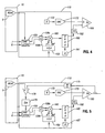
- FIG. 4 is a block diagram of an open loop configuration for an 8-PSK mode of operation in accordance with an embodiment of the present invention.
- FIG. 5 a block diagram of a closed loop configuration for an 8-PSK mode of operation in accordance with an embodiment of the present invention.
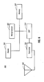
- FIG. 6 is a block diagram of a system in accordance with one embodiment of the present invention.
- a transceiver in accordance with an embodiment of the present invention may be used in handsets accommodating multi-mode wireless communications.
- a transceiver in accordance with an embodiment may be used in a GSM system to provide support for various communication protocols including GPRS and EDGE communication schemes. Accordingly, the transceiver may support both GMSK and 8-PSK modulation schemes.
- a transceiver in accordance with an embodiment of the present invention may include multiple transmission paths to support the various modulation schemes and provide for communication according to multiple protocols. Furthermore, to enable reduced size and power consumption, portions of the transmission paths may be reused in both schemes to reduce needed circuitry in a transceiver design. Still further, in various embodiments, the circuitry of the various transmission paths may include low noise circuitry to enable communication according to multiple schemes without degrading performance of any of the communication protocols, as well as avoiding leakage that causes interference in the airwaves at a frequency of closely located handsets' receive bands.
- an offset phase-locked loop (OPLL) of a first transmission path may be reused in multiple modes of operation.
- the OPLL may be modulated by incoming baseband data (e.g., complex in-phase and quadrature (I/Q) signals) in a GMSK mode.
- Such OPLL circuitry may be reused as a local oscillator (LO) in an 8-PSK mode of operation.
- LO local oscillator
- SNR signal-to-noise ratio
- no transmit surface acoustic wave (SAW) filter may be needed.
- Additional circuitry, e.g., of a second transmission path may also be reused in the different modes of operation.
- a mixer and digital variable gain amplifier (DVGA) of the second transmission path may be used in two modes.
- the mixer/DVGA operates to upconvert incoming baseband signals to a desired transmit frequency.
- the mixer may further operate in a GMSK mode in which the mixer substantially acts as a buffer for modulated signals received from the OPLL. In this mode of operation, the mixer may provide a fixed output power level corresponding to a desired saturation level for the GMSK mode of operation.
- a transceiver 110 may be implemented in a system 100 such as a wireless device, e.g., a cellular telephone handset, personal digital assistant (PDA) or other such device.
- Transceiver 110 may include both receive and transmit circuitry, although the transmit circuitry only is shown in the embodiment of FIG. 1 for ease of illustration.
- transceiver 110 is coupled to a baseband processor 10. Accordingly, baseband communication may occur between transceiver 110 and baseband processor 10.
- Transceiver 110 is further coupled to a power amplifier (PA) 180, which in turn is coupled to an antenna switch 190 that itself is coupled to an antenna 195.
- PA power amplifier
- transceiver 110 may be adapted in a single integrated circuit (IC) transceiver that includes both receive and transmit paths and various control circuitry therefor, in one embodiment. Further still, in some embodiments the transmit path may be a direct upconversion transmitter.
- transceiver 110 includes various circuitry to enable receipt of baseband signals from baseband processor 10 and processing thereof to provide RF outputs to PA 180. Accordingly, transceiver 110 includes a baseband interface 115 to provide coupling to baseband processor 10. Baseband interface 115 in turn is coupled to a multiplexer 120, which is controlled to provide outputs to different paths depending on the mode of operation (e.g., GMSK mode or 8-PSK mode). As shown in FIG 1 , baseband interface 115 is coupled in a bidirectional manner with baseband processor 10 to enable transmission and receipt of baseband I and Q signals, as well as the receipt of incoming control signals (e.g., a RAMPIN signal) from baseband processor 10.
- incoming control signals e.g., a RAMPIN signal
- baseband processor 10 may provide control signals which may pass through transceiver 110 to control PA 180.
- the incoming ramp signal from baseband processor 10 may be an analog signal generated by a ramp digital-to-analog converter (DAC) in baseband processor 10.
- DAC digital-to-analog converter
- multiplexer 120 may provide incoming baseband signals to a selected one of multiple transmission paths.
- FIG. 1 shows a dual transmitter design in which different transmit paths are present. These different paths may be controlled differently in different modes of operation. For example, in a GMSK mode, incoming I/Q signals are provided to a first transmission path including the OPLL, while in an 8-PSK mode, incoming I/Q signals are provided to a second transmission path including the mixer/DVGA, as discussed above.
- I and Q data is provided to the first transmission path that includes a mixer 130 which may be an intermediate frequency (IF) mixer running at a frequency of approximately 500 MHz, which is controlled to mix the incoming signals with a frequency provided by a frequency synthesizer 125.
- the signals from frequency synthesizer 125 provided to mixer 130 are used to upconvert the incoming baseband I and Q signals to a desired intermediate frequency.
- the IF signals provided from frequency synthesizer 125 to mixer 130 may be set at a fixed value. For purposes of discussions herein, such signals may be provided at a fixed frequency D. Accordingly, the output of mixer 130 provides modulated signals at this intermediate frequency D.
- the OPLL may include a phase detector 140, which is coupled to receive the upconverted modulated signals from mixer 130. As further shown in FIG. 1 , phase detector 140 is further coupled to receive an output from a mixer 145. Mixer 145 in turn is controlled via another output from frequency synthesizer 125. For purposes of discussion herein, this output may be at a frequency C. In various embodiments, C may be controllable to vary the input to mixer 145 via the action of feedback. For purposes of discussions herein, the output of mixer 145 may be at a frequency B.
- phase detector 140 in conjunction with the other components of the OPLL will drive B to equal D.
- phase detector 140 is provided to a filter 135.
- the filtered output is fed to a local oscillator (LO) 150 that is coupled in a feedback loop with mixer 145.
- the output (B) of mixer 145 equals the sum/difference of the inputs thereto, namely the output of LO 150, A, and the output of frequency synthesizer 125, C.
- LO local oscillator
- B A ⁇ C
- A D ⁇ C
- the output of LO 150 i.e., A
- a modulated signal generated at a desired frequency A which is output to a divider/quadrature phase shifter 152 which provides complex signals to a mixer 160 of the second transmission path.
- Divider/shifter 152 may be configured, for example, as a divide by 2 or divide by 4, in various implementations, or other integers.
- the OPLL is a suitable design for use in various applications such as a GMSK modulation scheme since the OPLL can generate signals with very low noise.
- This low noise in part is due to the presence of filter 135, which filters noise generated in various noisy components of the first path, including phase detector 140 and mixer 130, as well as other noise inherent in the circuit.
- filter 135 filters noise generated in various noisy components of the first path, including phase detector 140 and mixer 130, as well as other noise inherent in the circuit.
- use of the OPLL provides for suitable SNRs, preventing noise from leaking into the GSM receive bands of other handsets.
- the reduced noise effects using the OPLL allow a design that consumes less power and chip area. Still further, the need for an off-chip SAW filter may be avoided.
- Filter 135 thus allows modulated signals to pass to LO 150 in GMSK mode, while preventing noise from front-end components of transceiver 110 from being passed.
- a mixer 160 and DVGA 165 of the second transmission path may form a digital variable gain mixer. That is, while shown as separate components in the embodiment of FIG. 1 , mixer 160 and DVGA 165 may be implemented with unified circuitry, in some embodiments. Note that a single mixer and DVGA is shown for ease of illustration in the embodiment of FIG. 1 . However, it is to be understood that in many implementations multiple mixers and DVGAs may be present to provide outputs at different frequency bands (e.g., 900 MHz and 1800 MHz). Further, such different DVGAs may be independently gain-controlled for different power levels for a given frequency band.
- GMSK mode of operation at least portions of mixer 160 may be powered down and a single incoming current from the baseband path of the second transmission path may act as a DC current, with an incoming signal from LO 150 of the first transmission path providing the signal modulation.
- modulated I/Q signals provided from LO 150 are provided to mixer 160, which substantially acts as a buffer to mix the modulated signals with a DC baseband current (which may be a single baseband path), and provide an output to DVGA 165.
- Transceiver 110 may be coupled to a PA 180 that receives the RF signals from transceiver 110. Furthermore, as shown in FIG. 1 , PA 180 may be controlled via signals received from transceiver 110. In various embodiments, transceiver 110 further includes a power amplifier controller 170 to control PA 180. However, depending on a system in which transceiver 110 is adapted, control of PA 180 may come from the baseband processor 10 or in another desired manner.
- the second transmission path of transceiver 110 enables transmission of signals of a different mode of operation than the first transmission path.
- the second transmission path is coupled to receive I and Q data from multiplexer 120 at a pair of analog variable gain amplifiers/attenuators (AVGAs) 155a and 155b (generically AVGA 155).
- a gain level (which may be an attenuation level) of AVGA 155 may be controlled with an analog or continuous signal.
- the output signals from these amplifiers/attenuators may be filtered in respective low pass filters (LPFs) 158a and 158b (generically LPF 158).
- LPFs low pass filters
- Filters 158 may be LPFs because these signals are in the transmission path at baseband frequencies.
- AVGAs 155a and 155b may be controlled by ramp signals received from baseband processor 10.
- ramp signals alternatively may be provided from baseband processor 10 directly to PA 180. Accordingly, to enable use of transceiver 110 with chips of various manufacturers, AVGAs 155a and 155b may be variably controlled to provide a desired gain/attenuation as needed for a particular system in which transceiver 110 is located.
- portions of the first transmission path may be reused for 8-PSK modes. More specifically, portions of the first transmission path may be used to enable operation in an 8-PSK mode with minimal additional circuitry (i.e., AVGAs 155 and filters 158).
- the first transmission path is used to create a constant wave (CW) carrier signal. Noise is still a concern, but the noise requirements for 8-PSK mode are slightly relaxed as compared to GMSK mode. Accordingly, a minimal amount of additional circuitry (and therefore additional noise) to implement 8-PSK transmissions may be present.
- mixer 160 receives baseband currents from the second transmission path which are mixed with an unmodulated pure carrier signal from LO 150.
- mixer 160 may be a commutating mixer, rather than a multiplier-based mixer. In this way, reduced noise is realized, as switches that form the mixer may be of relatively low noise.
- Such a commutating mixer may operate by applying square wave signals (i.e., switching on and off of switches) to an incoming baseband signal.
- Mixer 160 and DVGA 165 in 8-PSK mode may be digitally controlled to provide output power control of at least 40 dB and further to provide such control with a fine step, e.g., 0.5 dB per step.
- Mixer 160 may be implemented as a plurality of circuitry slices individually controllable to attain a desired gain level.
- the unselected transmission path may be provided with predetermined constant values in order to provide for desired operation.
- the second path may be provided with full scale and zero scale signals, respectively, along the I and Q paths.
- the I portion of mixer 160 may be enabled such that modulated signals from the first path may be passed through DVGA 165, acting as a buffer.
- at least one of the mixers of complex mixer 130 may be provided with a constant full scale value so that the unmodulated frequency signal from frequency synthesizer 125 may be provided to phase detector 140 in order to generate the desired unmodulated carrier signal.
- the architecture of FIG. 1 may also be considered to be a two-transmission path architecture with an additional common output path shared by the transmission paths. That is, at least portions of mixer 160 and DVGA 165 may be considered to be a common output path that is used in multiple modes of operation to enable transmission of RF signals processed in the first and second transmission paths. While described with this particular implementation in the embodiment of FIG. 1 , it is to be understood that the scope of the present invention is not so limited and transceivers may take different forms in other embodiments.
- a transceiver in accordance with an embodiment of the present invention may be controlled in an open loop or closed loop fashion.
- FIG. 2 shown is a block diagram of an open loop implementation for a GMSK mode of operation. Note that the use of the same reference numerals in FIG. 2 as in FIG. 1 corresponds to the same components, and further note that only a few selected components of the transceiver and related components are shown for ease of illustration in FIG. 2 .
- an analog power level signal for PA 180 may be provided directly from a baseband processor 10 and more specifically from a ramp DAC 5. This analog power level signal may be used to perform ramp activities, depending on operation requirements.
- the power level signal may provide ramp control for PA 180, or an active power level.
- transceiver 110 may be controlled to provide fixed input signals to mixer 160 (i.e., full scale and zero scale signals), e.g., from a second transmission path, while incoming modulated signals are provided to mixer 160 via phase shifter/frequency divider 152.
- incoming modulated signals to phase shifter 152 may be provided at 4 GHz.
- Mixer 160 provides a modulated output to DVGA 165, which may be controlled by information in a register 167. The information may correspond to a nominal level for control of DVGA 165.
- the RF output from DVGA 165 is thus provided to PA 180, where the RF signal is controlled according to the analog power level signal received from baseband processor 10.
- the analog power level signal may be passed through transceiver 110.
- FIG. 3 shown is a block diagram of a closed loop configuration for a GMSK mode in accordance with an embodiment of the present invention.
- a feedback path is coupled from the output of PA 180 back to transceiver 110. More specifically, the feedback path is coupled through a level detector 175 and is provided to an amplifier 178, where a difference between the detected feedback information and the analog power level signal is amplified.
- PA 180 is thus controlled based on the output of amplifier 178.
- the transmission path is the same as that shown and described with regard to FIG. 2 above.
- a transceiver in accordance with an embodiment of the present invention may be controlled in either open loop or closed loop fashion for an 8-PSK mode of operation.
- FIG. 4 shown is a block diagram of an open loop configuration for an 8-PSK mode of operation in accordance with an embodiment of the present invention.
- incoming I and Q data i.e., obtained from baseband processor 10
- a variable attenuator 155 which may correspond to AVGA 155 shown in FIG. 1
- ramp DAC 5 of baseband processor 10 may provide ramp signals to variable attenuator 155.
- the attenuated signals may be provided through low pass filters 158a and 158b to mixer 160, where they are mixed with incoming unmodulated (i.e., continuous wave) signals which are at the channel frequency from phase shifter/frequency divider 152.
- the output from mixer 160 is provided to DVGA 165, which may be controlled via register 167.
- the output from DVGA 165 may be filtered by a harmonic filter 182, in some implementations.
- a nominal voltage level for the PA may be generated from a nominal level stored in a register 172 that is provided to a DAC 173 that in turn generates an analog voltage to provide for control of PA 180.
- FIG. 5 shown is a block diagram of a closed loop configuration for an 8-PSK mode of operation in accordance with an embodiment of the present invention.
- a feedback path from the output of PA 180 is coupled through a level detector 175 and provided to an amplifier 178, which amplifies a difference between the detected feedback signal and the output of ramp DAC 5 of baseband processor 10.
- the output of amplifier 178 is provided to a sample and hold circuit 179, which may be used to disable feedback after ramp up and before ramp down.
- the output of sample and hold circuit 179 is in turn used to control variable attenuator 155. While shown with these particular implementations of open loop and closed loop configurations in the embodiments of FIGS. 2-5 , it is to be understood that the scope of the present invention is not limited to these particular configurations, and other manners of controlling a transceiver in accordance with an embodiment of the present invention may be implemented.
- a transceiver in accordance with an embodiment of the present invention can be implemented in many different systems.
- system 305 may be a cellular telephone handset, although the scope of the present invention is not so limited.
- the system may be a pager, personal digital assistant (PDA) or other such device.
- PDA personal digital assistant
- an antenna 302 may be coupled to a transceiver 102, which may correspond to transceiver 110 of FIG. 1 .
- transceiver 102 may be coupled to a digital signal processor (DSP) 310, which may handle processing of baseband communication signals.
- DSP digital signal processor
- DSP 310 may be coupled to a microprocessor 320, such as a central processing unit (CPU) that may be used to control operation of system 305 and further handle processing of application programs, such as personal information management (PIM) programs, email programs, downloaded games, and the like.
- microprocessor 320 and DSP 310 may also be coupled to a memory 330.
- Memory 330 may include different memory components, such as a flash memory and a read only memory (ROM), although the scope of the present invention is not so limited.
- a display 340 may be present to provide display of information associated with telephone calls and application programs.
- transceiver 102 and/or DSP 310 may include an article in the form of a machine-readable storage medium (or may be coupled to such an article, e.g., memory 330) onto which there are stored instructions and data that form a software program.
- the software program may provide for control of transceiver 102, e.g., for controlling transmission of RF signals according to multiple communication protocols along at least several transmission paths, e.g., via control of which transmission path is selected and control of the selected transmission path (e.g., frequency, gain, timing and so forth) and non-selected path (e.g., via input of predetermined values).
Landscapes
- Engineering & Computer Science (AREA)
- Signal Processing (AREA)
- Computer Networks & Wireless Communication (AREA)
- Transmitters (AREA)
- Digital Transmission Methods That Use Modulated Carrier Waves (AREA)
- Transceivers (AREA)
- Communication Control (AREA)
Claims (16)
- Vorrichtung, umfassend:einen ersten Übertragungspfad (120, 130, 140, 135, 150, 152), um Basisbandsignale für ein erstes drahtloses Kommunikationsprotokoll in einer ersten Betriebsart zu empfangen und zu verarbeiten, um ein Radiofrequenzsignal (RF-Signal) für Output über einen gemeinsamen Outputpfad (160, 165, 180, 190, 195) zu generieren; undeinen zweiten Übertragungspfad (120, 155, 158), um die Basisbandsignale für ein zweites drahtloses Kommunikationsprotokoll in einer zweiten Betriebsart zu empfangen und zu verarbeiten, um ein Radiofrequenzsignal (RF-Signal) für Output über einen gemeinsamen Output-Pfad (160, 165, 180, 190, 195) zu generieren;wobei die Vorrichtung zumindest einen Teil des ersten Übertragungspfads in der zweiten Betriebsart wiederverwenden soll, wobei der erste Übertragungspfad dem zweiten Übertragungspfad in der zweiten Betriebsart ein Trägersignal bereitstellen soll;dadurch gekennzeichnet, dass:ein Multiplexer (120) eingerichtet ist, einem selektierten Pfad der ersten und zweiten Übertragungspfade in den ersten bzw. zweiten Betriebsarten die ankommenden Basisbandsignale bereitzustellen;der erste Übertragungspfad einen Offset-Phasenregelkreis (OPLL) umfasst, der einschließt:einen Phasendetektor (140), der an einen Output eines ersten OPPL-Mischers (130) gekoppelt ist, wobei der Phasendetektor (140) weiter gekoppelt ist, ein Rückkopplungssignal von einem zweiten OPPL-Mischer (145) zu empfangen;ein Filter (135) gekoppelt ist, einen Output des Phasendetektors (140) zu empfangen und zu filtern;ein lokaler Oszillator (150) an einen Output des Filters (135) gekoppelt ist, um ein moduliertes Signal in der ersten Betriebsart auszugeben, wobei der lokale Oszillator (150) ein nicht moduliertes Signal in der zweiten Betriebsart ausgeben soll; undder zweite OPPL-Mischer (145) gekoppelt ist, einen Output des lokalen Oszillators (150) zu empfangen;der lokale Oszillator (150) gekoppelt ist, dem Mischer (160) des zweiten Übertragungspfads das modulierte Signal in der ersten Betriebsart bereitzustellen; andder zweite Übertragungspfad umfasst;einen Analogverstärker (155), der gekoppelt ist, die Basisbanddaten zu empfangen; undeinen Filter (158), der zwischen einem Output des Analogverstärkers (155) und dem Mischer (160) des zweiten Übertragungspfads gekoppelt ist.
- Vorrichtung nach Anspruch 1, wobei der Mischer (160) des zweiten Übertragungspfads das modulierte Signal puffern und dem gemeinsamen Output-Pfad bereitstellen soll.
- Vorrichtung nach Anspruch 1, wobei der Offset-Phasenregelkreis (OPLL) dem Mischer (160) des zweiten Übertragungspfads das nicht modulierte Signal in der zweiten Betriebsart bereitstellen soll.
- Vorrichtung nach Anspruch 3, wobei der Mischer (160) des zweiten Übertragungspfads die Basisbanddaten mit dem nicht modulierten Signal in der zweiten Betriebsart mischen soll.
- Vorrichtung nach Anspruch 1, wobei das RF-Signal Amplituden- und Phaseninformation in der zweiten Betriebsart einschließt.
- Vorrichtung nach Anspruch 5, wobei die erste Betriebsart einen GMSK-Modulationsplan einschließt und die zweite Betriebsart einen 8-PSK-Modulationplan einschließt.
- System, das die Vorrichtung des Anspruchs 1 umfasst, wobei:der erste Sendepfad (120, 130, 140, 135, 150, 152) ein (GMSK-) gaußsches Minimalphasenumtastungs-Radiofrequenzsignal (RF-Signal) in einer GMSK-Betriebsart generieren soll;der zweite Sendepfad (120, 155, 158) ein 8-Phasenumtastungs-Radiofrequenzsignal (8-PSK-RF-Signal) in einer 8-PSK-Betriebsart generieren soll, wobei der zweite Sendepfad (120, 155, 158) ein Trägersignal vom ersten Sendepfad (120, 130, 140, 135, 150, 152), während der 8-PSK-Betriebsart, empfangen soll und, wobei der zweite Sendepfad (120, 155, 158) das GMSK-RF-Signal in der GMSK-Betriebsart puffern soll; undein Leistungsverstärker (180) an den zweiten Sendepfad gekoppelt ist.
- System nach Anspruch 7, wobei der erste Sendepfad umfasst:einen Phasendetektor (140), der an einen Output eines ersten Mischers (130) gekoppelt ist, wobei der Phasendetektor weiter gekoppelt ist, ein Rückkopplungssignal von einem zweiten Mischer (145) zu empfangen;einen Filter (135), der gekoppelt ist, einen Output des Phasendetektors (140) zu empfangen und zu filtern;einen lokalen Oszillator (150), der an einen Output des Filters (135) gekoppelt ist, um ein moduliertes Signal in der GMSK-Betriebsart auszugeben, wobei der lokale Oszillator (150) das nicht modulierte Trägersignal in der 8-PSK-Betriebsart ausgeben soll; undden zweiten Mischer (145), der gekoppelt ist, einen Output des lokalen Oszillators (150) zu empfangen.
- System nach Anspruch 8, wobei der zweite Sendepfad umfasst:einen Analogverstärker (155), der gekoppelt ist, die zweiten Basisbanddaten zu empfangen;einen Filter (158), der an einen Output des Analogverstärkers (155) gekoppelt ist; undeinen Mischer, der an einen Output des Filters gekoppelt ist, um die zweiten Basisbanddaten mit dem nicht modulierten Trägersignal vom ersten Sendepfad in der 8-PSK-Betriebsart zu mischen.
- System nach Anspruch 7, das weiter einen Sender-Empfänger (110) umfasst, der den ersten Sendepfad und den zweiten Sendepfad einschließt, wobei der Sender-Empfänger (110) in einer offenen Regelkreiskonfiguration oder in einer geschlossenen Regelkreiskonfiguration steuerbar ist.
- System nach Anspruch 10, das weiter einen Rückkopplungspfad umfasst, der gekoppelt ist, einen Output des Leistungsverstärkers (180) zu empfangen, wobei der Rückkopplungspfad weiter einen zweiten Verstärker (178) umfasst, um einen Unterschied zwischen einem Wert, der repräsentativ für den Output des Leistungsverstärkers (180) ist, und einem Referenzsignal zu verstärken, das von einem Basisbandprozessor empfangen wird, der an den Sender-Empfänger (110) gekoppelt ist.
- System nach Anspruch 9, das weiter einen Sender-Empfänger (110) umfasst, der den ersten Sendepfad und den zweiten Sendepfad einschließt, wobei der Sender-Empfänger in einer offenen Regelkreiskonfiguration oder in einer geschlossenen Regelkreiskonfiguration steuerbar ist.
- System nach Anspruch 12, das weiter einen Rückkopplungspfad umfasst, der gekoppelt ist, einen Output des Leistungsverstärkers (180) zu empfangen, wobei der Rückkopplungspfad weiter einen zweiten Verstärker (178) umfasst, um einen Unterschied zwischen einem Wert, der repräsentativ für den Output des Leistungsverstärkers (186) ist, und einem Referenzsignal zu verstärken, das von einem Basisbandprozessor empfangen wird, der an den Sender-Empfänger (110) gekoppelt ist, wobei ein Output des zweiten Verstärkers (178) den Analogverstärker (180) steuern soll.
- Verfahren, umfassend:in einer ersten Betriebsart (GMSK), Bereitstellen erster ankommenden Basisbandsignale an einen ersten Übertragungspfad (120, 130, 140, 135, 150, 152) eines Sender-Empfängers, wobei die ersten ankommenden Basisbandsignale für ein erstes drahtloses Kommunikationsprotokoll sind und Verarbeitung der ersten ankommenden Basisbandsignale in einem Offset-Phasenregelkreis (OPLL) (135, 140, 150) des ersten Übertragungspfads (120, 130, 140, 135, 150, 152), um erste Radiofrequenzsignale (RF-Signale) zu erhalten; undin einer zweiten Betriebsart (8-PSK), einem zweiten Übertragungspfad (120, 155, 158) eines Sender-Empfängers (110) zweite ankommende Basisbandsignale bereitzustellen, wobei die zweiten ankommenden Basisbandsignale für ein zweites drahtloses Kommunikationsprotokoll sind und Modulieren (160) eines Output-Signals des Offset-Phasenregelkreises (OPLL) (135, 140, 150) mit den zweiten ankommenden Basisbandsignalen, um zweite RF-Signale im zweiten Übertragungspfad (120, 155, 158) zu erhalten;dadurch gekennzeichnet, dass:ein Multiplexer (120) gesteuert wird, die ankommenden Basisbandsignale einem selektierten Pfad der ersten und zweiten Übertragungspfade in den ersten und zweiten Betriebsarten bereitzustellen; und durch Bereitstellen eines nicht modulierten Output-Signals des Offset-Phasenregelkreises (OPLL) (135, 140, 150) in der zweiten Spezifikationsart;der erste Übertragungspfad einen Offset-Phasenregelkreis (OPLL) umfasst, der einschließt:einen Phasendetektor (140), der an einen Output eines ersten OPPL-Mischers (130) gekoppelt ist, wobei der Phasendetektor (140) weiter gekoppelt ist, ein Rückkopplungssignal von einem zweiten OPPL-Mischer (145) zu empfangen;ein Filter (135) gekoppelt ist, einen Output des Phasendetektors (140) zu empfangen und zu filtern;ein lokaler Oszillator (150) an einen Output des Filters (135) gekoppelt ist, um ein moduliertes Signal in der ersten Betriebsart auszugeben, wobei der lokale Oszillator (150) ein nicht moduliertes Signal in der zweiten Betriebsart ausgeben soll; undder zweite OPPL-Mischer (145) gekoppelt ist, einen Output des lokalen Oszillators (150) zu empfangen;der lokale Oszillator (150) gekoppelt ist, dem Mischer (160) des zweiten Übertragungspfads das modulierte Signal in der ersten Betriebsart bereitzustellen; andder zweite Übertragungspfad umfasst;einen Analogverstärker (155), der gekoppelt ist, die Basisbanddaten zu empfangen; undeinen Filter (158), der zwischen einem Output des Analogverstärkers (155) und dem Mischer (160) des zweiten Übertragungspfads gekoppelt ist.
- Verfahren nach Anspruch 14, das weiter Bereitstellen eines festgelegten Inputs an den zweiten Übertragungspfad, während Bereitstellen der ersten ankommenden Basisbandsignale an den ersten Übertragungspfad, umfasst.
- Verfahren nach Anspruch 14, das weiter Steuern des ersten Übertragungspfads in Übereinstimmung mit einem Modell offenen Regelkreises oder einem Modell geschlossenen Regelkreises, beruhend auf einem System umfasst, in dem sich der Sender-Empfänger befindet.
Applications Claiming Priority (3)
| Application Number | Priority Date | Filing Date | Title |
|---|---|---|---|
| US72041305P | 2005-09-26 | 2005-09-26 | |
| US11/510,339 US7720176B2 (en) | 2005-09-26 | 2006-08-25 | Edge transceiver architecture and related methods |
| PCT/US2006/035289 WO2007037963A1 (en) | 2005-09-26 | 2006-09-12 | Edge transceiver architecture and related methods |
Publications (2)
| Publication Number | Publication Date |
|---|---|
| EP1932243A1 EP1932243A1 (de) | 2008-06-18 |
| EP1932243B1 true EP1932243B1 (de) | 2010-09-01 |
Family
ID=37663344
Family Applications (1)
| Application Number | Title | Priority Date | Filing Date |
|---|---|---|---|
| EP06814446A Ceased EP1932243B1 (de) | 2005-09-26 | 2006-09-12 | Edge-sende-empfangsarchitektur und entsprechende verfahren |
Country Status (6)
| Country | Link |
|---|---|
| US (1) | US7720176B2 (de) |
| EP (1) | EP1932243B1 (de) |
| JP (1) | JP4824759B2 (de) |
| AT (1) | ATE480051T1 (de) |
| DE (1) | DE602006016625D1 (de) |
| WO (1) | WO2007037963A1 (de) |
Families Citing this family (8)
| Publication number | Priority date | Publication date | Assignee | Title |
|---|---|---|---|---|
| US7583937B2 (en) * | 2005-04-26 | 2009-09-01 | Silicon Laboratories Inc. | Digital interface and related event manager for integrated circuits |
| US7697901B2 (en) | 2005-09-26 | 2010-04-13 | St-Ericsson Sa | Digital variable gain mixer |
| US7720176B2 (en) | 2005-09-26 | 2010-05-18 | St-Ericsson Sa | Edge transceiver architecture and related methods |
| US8023556B2 (en) * | 2007-03-30 | 2011-09-20 | Silicon Laboratories Inc. | Autonomously generating ramp profiles in a transceiver |
| US20090296853A1 (en) * | 2008-05-30 | 2009-12-03 | Zerog Wireless, Inc. | Rotation Direction Control for Phase Modulation |
| WO2016134319A1 (en) | 2015-02-19 | 2016-08-25 | Enphase Energy, Inc. | Method and apparatus for time-domain droop control with integrated phasor current control |
| US10338646B1 (en) | 2018-02-22 | 2019-07-02 | Lg Electronics Inc. | Radio frequency amplifier circuit and mobile terminal having the same |
| KR102040546B1 (ko) * | 2018-02-22 | 2019-11-06 | 엘지전자 주식회사 | 무선 주파수 증폭기 회로 및 이를 구비하는 이동 단말기 |
Family Cites Families (39)
| Publication number | Priority date | Publication date | Assignee | Title |
|---|---|---|---|---|
| US4700327A (en) | 1984-12-31 | 1987-10-13 | Raytheon Company | Digital memory system |
| US7065327B1 (en) | 1998-09-10 | 2006-06-20 | Intel Corporation | Single-chip CMOS direct-conversion transceiver |
| JP3960582B2 (ja) | 1999-10-28 | 2007-08-15 | 株式会社東芝 | 可変利得回路 |
| DE19956073C2 (de) * | 1999-11-22 | 2002-03-28 | Infineon Technologies Ag | Modulationsanordnung |
| JP4679686B2 (ja) | 2000-02-07 | 2011-04-27 | パナソニック株式会社 | 無線通信装置及び送信電力制御方法 |
| US6747987B1 (en) | 2000-02-29 | 2004-06-08 | Motorola, Inc. | Transmit modulation circuit and method of operating a transmitter |
| JP2002111400A (ja) | 2000-10-03 | 2002-04-12 | Nec Corp | 電力増幅器 |
| US6711391B1 (en) | 2000-10-10 | 2004-03-23 | Qualcomm, Incorporated | Gain linearizer for variable gain amplifiers |
| JP2002280842A (ja) | 2001-03-21 | 2002-09-27 | Hitachi Ltd | 電力増幅器モジュール |
| JP3816356B2 (ja) * | 2001-06-21 | 2006-08-30 | 株式会社東芝 | 無線送信機 |
| US7158494B2 (en) | 2001-10-22 | 2007-01-02 | Matsushita Electric Industrial Co., Ltd. | Multi-mode communications transmitter |
| EP1341300A1 (de) | 2002-02-27 | 2003-09-03 | Lucent Technologies Inc. | Leistungsverstärker mit einstellbarer Ruhestromeinstellung |
| DE10209516A1 (de) | 2002-03-04 | 2003-07-17 | Infineon Technologies Ag | Sendeanordnung |
| SE521746C2 (sv) | 2002-04-05 | 2003-12-02 | Ericsson Telefon Ab L M | Multimoduleringssändare |
| EP1367842A1 (de) * | 2002-05-29 | 2003-12-03 | Siemens Aktiengesellschaft | Schaltungsanordnung zum Umschalten eines Mobilfunksenders zwischen zwei Modulationsbetriebsarten |
| GB2412512B (en) | 2002-05-31 | 2005-11-16 | Renesas Tech Corp | A communication semiconductor integrated circuit, a wireless communication apparatus, and a loop gain calibration method |
| WO2004021659A1 (en) | 2002-08-28 | 2004-03-11 | Philips Intellectual Property & Standards Gmbh | Method for generating i/q signal in a tdma transmitter and corresponding modulator |
| US7233774B2 (en) | 2003-01-30 | 2007-06-19 | Broadcom Corporation | RF transceiver with compact stacked mixer design for multiple frequency conversion |
| US7010330B1 (en) | 2003-03-01 | 2006-03-07 | Theta Microelectronics, Inc. | Power dissipation reduction in wireless transceivers |
| JP4163531B2 (ja) | 2003-03-06 | 2008-10-08 | 三星電子株式会社 | 自動利得制御装置 |
| US7444124B1 (en) | 2003-05-14 | 2008-10-28 | Marvell International Ltd. | Adjustable segmented power amplifier |
| JP4713852B2 (ja) | 2003-08-28 | 2011-06-29 | ルネサスエレクトロニクス株式会社 | 周波数発生回路及びそれを用いた通信システム |
| US7010057B2 (en) | 2003-09-04 | 2006-03-07 | Nokia Corporation | Dual mode multi-slot EGPRS transmitter |
| US6812771B1 (en) | 2003-09-16 | 2004-11-02 | Analog Devices, Inc. | Digitally-controlled, variable-gain mixer and amplifier structures |
| JP4289667B2 (ja) | 2003-09-16 | 2009-07-01 | ソニー・エリクソン・モバイルコミュニケーションズ株式会社 | 可変利得制御回路および受信装置 |
| WO2005088922A1 (en) | 2004-03-04 | 2005-09-22 | Qualcomm Incorporated | A method of and an apparatus for effecting a smooth transition between adjacent symbol bursts transmitted in different modulation formats |
| US7421259B2 (en) | 2004-04-16 | 2008-09-02 | Broadcom Corporation | RF mixer with high local oscillator linearity using multiple local oscillator phases |
| US7369822B2 (en) | 2004-05-18 | 2008-05-06 | Sige Semiconductor Inc. | Segmented switching power amplifier |
| US7602246B2 (en) | 2004-06-02 | 2009-10-13 | Qualcomm, Incorporated | General-purpose wideband amplifier |
| US20060214842A1 (en) | 2004-06-29 | 2006-09-28 | Kyocera Corporation | Mixer, High-Frequency transmitting/receiving apparatus having the same, radarapparatus having the high-frequency transmitting/receiving apparatus, and vehicle equipped with radar apparatus |
| US7161423B2 (en) | 2004-06-30 | 2007-01-09 | Silicon Laboratories Inc. | Parallel power amplifier and associated methods |
| US7359449B2 (en) * | 2004-10-05 | 2008-04-15 | Kamilo Feher | Data communication for wired and wireless communication |
| US7394862B2 (en) * | 2004-12-21 | 2008-07-01 | Broadcom Corporation | Multi-mode wireless polar transmitter architecture |
| US7400866B2 (en) | 2005-01-14 | 2008-07-15 | General Instrument Corporation | Methods and apparatus for calibrating and controlling output power levels in a broadband communication system |
| US7292101B2 (en) | 2005-04-27 | 2007-11-06 | Broadcom Corporation | Digitally adjustable variable gain amplifier (VGA) using switchable differential pairs |
| US7720176B2 (en) | 2005-09-26 | 2010-05-18 | St-Ericsson Sa | Edge transceiver architecture and related methods |
| US7697901B2 (en) | 2005-09-26 | 2010-04-13 | St-Ericsson Sa | Digital variable gain mixer |
| US7415257B2 (en) | 2005-10-14 | 2008-08-19 | Kuei-ann Wen | Dual-band mixer and its design flow |
| US7542741B2 (en) | 2006-01-31 | 2009-06-02 | Skyworks Solutions, Inc. | System and method for power mapping to compensate for power amplifier gain control variations |
-
2006
- 2006-08-25 US US11/510,339 patent/US7720176B2/en not_active Expired - Fee Related
- 2006-09-12 WO PCT/US2006/035289 patent/WO2007037963A1/en not_active Ceased
- 2006-09-12 DE DE602006016625T patent/DE602006016625D1/de active Active
- 2006-09-12 EP EP06814446A patent/EP1932243B1/de not_active Ceased
- 2006-09-12 JP JP2008532269A patent/JP4824759B2/ja not_active Expired - Fee Related
- 2006-09-12 AT AT06814446T patent/ATE480051T1/de not_active IP Right Cessation
Also Published As
| Publication number | Publication date |
|---|---|
| JP4824759B2 (ja) | 2011-11-30 |
| US20070071129A1 (en) | 2007-03-29 |
| JP2009510832A (ja) | 2009-03-12 |
| DE602006016625D1 (de) | 2010-10-14 |
| ATE480051T1 (de) | 2010-09-15 |
| US7720176B2 (en) | 2010-05-18 |
| WO2007037963A1 (en) | 2007-04-05 |
| EP1932243A1 (de) | 2008-06-18 |
Similar Documents
| Publication | Publication Date | Title |
|---|---|---|
| US6795712B1 (en) | System for allowing a TDMA/CDMA portable transceiver to operate with closed loop power control | |
| US7376116B2 (en) | Software defined multiple transmit architecture | |
| US7483678B2 (en) | Single chip GSM/EDGE transceiver architecture with closed loop power control | |
| US7424276B2 (en) | Transmitter and wireless communication apparatus using the transmitter | |
| US7539462B2 (en) | Configurable multi-mode modulation system and transmitter | |
| US8755758B2 (en) | Technique for suppressing noise in a transmitter device | |
| KR101387262B1 (ko) | 직교 믹서를 위한 lo 신호 생성 시스템 및 방법 | |
| US7082169B2 (en) | Mirror translation loop transmitter architecture | |
| WO2008027295A2 (en) | Adaptive predistortion for controlling an open loop power amplifier | |
| US7369871B2 (en) | System and method for allowing a TDMA/CDMA portable transceiver to operate with closed loop power control | |
| JP4894503B2 (ja) | 無線通信装置 | |
| US7720176B2 (en) | Edge transceiver architecture and related methods | |
| CN101273533B (zh) | Edge收发机设备、系统及相关方法 | |
| EP1932244B1 (de) | Kontrolle der stromausgabe eines sende-empfangsgeräts | |
| KR100927650B1 (ko) | 이동통신 단말기용 송신기 및 그것의 송신 방법 | |
| JP4806575B2 (ja) | 送信装置 | |
| EP1014591A2 (de) | Linearisierungsschaltung eines Senders | |
| JP2004128863A (ja) | 無線通信装置 |
Legal Events
| Date | Code | Title | Description |
|---|---|---|---|
| PUAI | Public reference made under article 153(3) epc to a published international application that has entered the european phase |
Free format text: ORIGINAL CODE: 0009012 |
|
| 17P | Request for examination filed |
Effective date: 20080428 |
|
| AK | Designated contracting states |
Kind code of ref document: A1 Designated state(s): AT BE BG CH CY CZ DE DK EE ES FI FR GB GR HU IE IS IT LI LT LU LV MC NL PL PT RO SE SI SK TR |
|
| 17Q | First examination report despatched |
Effective date: 20080821 |
|
| GRAJ | Information related to disapproval of communication of intention to grant by the applicant or resumption of examination proceedings by the epo deleted |
Free format text: ORIGINAL CODE: EPIDOSDIGR1 |
|
| GRAP | Despatch of communication of intention to grant a patent |
Free format text: ORIGINAL CODE: EPIDOSNIGR1 |
|
| DAX | Request for extension of the european patent (deleted) | ||
| GRAS | Grant fee paid |
Free format text: ORIGINAL CODE: EPIDOSNIGR3 |
|
| GRAA | (expected) grant |
Free format text: ORIGINAL CODE: 0009210 |
|
| AK | Designated contracting states |
Kind code of ref document: B1 Designated state(s): AT BE BG CH CY CZ DE DK EE ES FI FR GB GR HU IE IS IT LI LT LU LV MC NL PL PT RO SE SI SK TR |
|
| REG | Reference to a national code |
Ref country code: GB Ref legal event code: FG4D |
|
| REG | Reference to a national code |
Ref country code: CH Ref legal event code: EP |
|
| REG | Reference to a national code |
Ref country code: IE Ref legal event code: FG4D |
|
| REF | Corresponds to: |
Ref document number: 602006016625 Country of ref document: DE Date of ref document: 20101014 Kind code of ref document: P |
|
| RAP2 | Party data changed (patent owner data changed or rights of a patent transferred) |
Owner name: ST-ERICSSON SA |
|
| REG | Reference to a national code |
Ref country code: GB Ref legal event code: 732E Free format text: REGISTERED BETWEEN 20101104 AND 20101110 |
|
| REG | Reference to a national code |
Ref country code: NL Ref legal event code: VDEP Effective date: 20100901 |
|
| PG25 | Lapsed in a contracting state [announced via postgrant information from national office to epo] |
Ref country code: AT Free format text: LAPSE BECAUSE OF FAILURE TO SUBMIT A TRANSLATION OF THE DESCRIPTION OR TO PAY THE FEE WITHIN THE PRESCRIBED TIME-LIMIT Effective date: 20100901 Ref country code: LT Free format text: LAPSE BECAUSE OF FAILURE TO SUBMIT A TRANSLATION OF THE DESCRIPTION OR TO PAY THE FEE WITHIN THE PRESCRIBED TIME-LIMIT Effective date: 20100901 Ref country code: FI Free format text: LAPSE BECAUSE OF FAILURE TO SUBMIT A TRANSLATION OF THE DESCRIPTION OR TO PAY THE FEE WITHIN THE PRESCRIBED TIME-LIMIT Effective date: 20100901 |
|
| LTIE | Lt: invalidation of european patent or patent extension |
Effective date: 20100901 |
|
| PG25 | Lapsed in a contracting state [announced via postgrant information from national office to epo] |
Ref country code: CY Free format text: LAPSE BECAUSE OF FAILURE TO SUBMIT A TRANSLATION OF THE DESCRIPTION OR TO PAY THE FEE WITHIN THE PRESCRIBED TIME-LIMIT Effective date: 20100901 Ref country code: PL Free format text: LAPSE BECAUSE OF FAILURE TO SUBMIT A TRANSLATION OF THE DESCRIPTION OR TO PAY THE FEE WITHIN THE PRESCRIBED TIME-LIMIT Effective date: 20100901 Ref country code: SI Free format text: LAPSE BECAUSE OF FAILURE TO SUBMIT A TRANSLATION OF THE DESCRIPTION OR TO PAY THE FEE WITHIN THE PRESCRIBED TIME-LIMIT Effective date: 20100901 |
|
| PG25 | Lapsed in a contracting state [announced via postgrant information from national office to epo] |
Ref country code: LV Free format text: LAPSE BECAUSE OF FAILURE TO SUBMIT A TRANSLATION OF THE DESCRIPTION OR TO PAY THE FEE WITHIN THE PRESCRIBED TIME-LIMIT Effective date: 20100901 Ref country code: NL Free format text: LAPSE BECAUSE OF FAILURE TO SUBMIT A TRANSLATION OF THE DESCRIPTION OR TO PAY THE FEE WITHIN THE PRESCRIBED TIME-LIMIT Effective date: 20100901 Ref country code: SE Free format text: LAPSE BECAUSE OF FAILURE TO SUBMIT A TRANSLATION OF THE DESCRIPTION OR TO PAY THE FEE WITHIN THE PRESCRIBED TIME-LIMIT Effective date: 20100901 Ref country code: GR Free format text: LAPSE BECAUSE OF FAILURE TO SUBMIT A TRANSLATION OF THE DESCRIPTION OR TO PAY THE FEE WITHIN THE PRESCRIBED TIME-LIMIT Effective date: 20101202 |
|
| PG25 | Lapsed in a contracting state [announced via postgrant information from national office to epo] |
Ref country code: MC Free format text: LAPSE BECAUSE OF NON-PAYMENT OF DUE FEES Effective date: 20100930 |
|
| REG | Reference to a national code |
Ref country code: CH Ref legal event code: PL |
|
| PG25 | Lapsed in a contracting state [announced via postgrant information from national office to epo] |
Ref country code: EE Free format text: LAPSE BECAUSE OF FAILURE TO SUBMIT A TRANSLATION OF THE DESCRIPTION OR TO PAY THE FEE WITHIN THE PRESCRIBED TIME-LIMIT Effective date: 20100901 Ref country code: SK Free format text: LAPSE BECAUSE OF FAILURE TO SUBMIT A TRANSLATION OF THE DESCRIPTION OR TO PAY THE FEE WITHIN THE PRESCRIBED TIME-LIMIT Effective date: 20100901 Ref country code: CZ Free format text: LAPSE BECAUSE OF FAILURE TO SUBMIT A TRANSLATION OF THE DESCRIPTION OR TO PAY THE FEE WITHIN THE PRESCRIBED TIME-LIMIT Effective date: 20100901 Ref country code: IS Free format text: LAPSE BECAUSE OF FAILURE TO SUBMIT A TRANSLATION OF THE DESCRIPTION OR TO PAY THE FEE WITHIN THE PRESCRIBED TIME-LIMIT Effective date: 20110101 Ref country code: PT Free format text: LAPSE BECAUSE OF FAILURE TO SUBMIT A TRANSLATION OF THE DESCRIPTION OR TO PAY THE FEE WITHIN THE PRESCRIBED TIME-LIMIT Effective date: 20110103 Ref country code: IT Free format text: LAPSE BECAUSE OF FAILURE TO SUBMIT A TRANSLATION OF THE DESCRIPTION OR TO PAY THE FEE WITHIN THE PRESCRIBED TIME-LIMIT Effective date: 20100901 Ref country code: RO Free format text: LAPSE BECAUSE OF FAILURE TO SUBMIT A TRANSLATION OF THE DESCRIPTION OR TO PAY THE FEE WITHIN THE PRESCRIBED TIME-LIMIT Effective date: 20100901 |
|
| PG25 | Lapsed in a contracting state [announced via postgrant information from national office to epo] |
Ref country code: ES Free format text: LAPSE BECAUSE OF FAILURE TO SUBMIT A TRANSLATION OF THE DESCRIPTION OR TO PAY THE FEE WITHIN THE PRESCRIBED TIME-LIMIT Effective date: 20101212 Ref country code: BE Free format text: LAPSE BECAUSE OF FAILURE TO SUBMIT A TRANSLATION OF THE DESCRIPTION OR TO PAY THE FEE WITHIN THE PRESCRIBED TIME-LIMIT Effective date: 20100901 |
|
| PLBE | No opposition filed within time limit |
Free format text: ORIGINAL CODE: 0009261 |
|
| STAA | Information on the status of an ep patent application or granted ep patent |
Free format text: STATUS: NO OPPOSITION FILED WITHIN TIME LIMIT |
|
| PG25 | Lapsed in a contracting state [announced via postgrant information from national office to epo] |
Ref country code: LI Free format text: LAPSE BECAUSE OF NON-PAYMENT OF DUE FEES Effective date: 20100930 Ref country code: CH Free format text: LAPSE BECAUSE OF NON-PAYMENT OF DUE FEES Effective date: 20100930 Ref country code: IE Free format text: LAPSE BECAUSE OF NON-PAYMENT OF DUE FEES Effective date: 20100912 |
|
| 26N | No opposition filed |
Effective date: 20110606 |
|
| PG25 | Lapsed in a contracting state [announced via postgrant information from national office to epo] |
Ref country code: DK Free format text: LAPSE BECAUSE OF FAILURE TO SUBMIT A TRANSLATION OF THE DESCRIPTION OR TO PAY THE FEE WITHIN THE PRESCRIBED TIME-LIMIT Effective date: 20100901 |
|
| REG | Reference to a national code |
Ref country code: DE Ref legal event code: R097 Ref document number: 602006016625 Country of ref document: DE Effective date: 20110606 |
|
| PG25 | Lapsed in a contracting state [announced via postgrant information from national office to epo] |
Ref country code: LU Free format text: LAPSE BECAUSE OF NON-PAYMENT OF DUE FEES Effective date: 20100912 Ref country code: BG Free format text: LAPSE BECAUSE OF FAILURE TO SUBMIT A TRANSLATION OF THE DESCRIPTION OR TO PAY THE FEE WITHIN THE PRESCRIBED TIME-LIMIT Effective date: 20100901 Ref country code: HU Free format text: LAPSE BECAUSE OF FAILURE TO SUBMIT A TRANSLATION OF THE DESCRIPTION OR TO PAY THE FEE WITHIN THE PRESCRIBED TIME-LIMIT Effective date: 20110302 |
|
| PG25 | Lapsed in a contracting state [announced via postgrant information from national office to epo] |
Ref country code: TR Free format text: LAPSE BECAUSE OF FAILURE TO SUBMIT A TRANSLATION OF THE DESCRIPTION OR TO PAY THE FEE WITHIN THE PRESCRIBED TIME-LIMIT Effective date: 20100901 |
|
| PG25 | Lapsed in a contracting state [announced via postgrant information from national office to epo] |
Ref country code: BG Free format text: LAPSE BECAUSE OF FAILURE TO SUBMIT A TRANSLATION OF THE DESCRIPTION OR TO PAY THE FEE WITHIN THE PRESCRIBED TIME-LIMIT Effective date: 20101201 |
|
| REG | Reference to a national code |
Ref country code: FR Ref legal event code: PLFP Year of fee payment: 11 |
|
| REG | Reference to a national code |
Ref country code: DE Ref legal event code: R082 Ref document number: 602006016625 Country of ref document: DE Representative=s name: GRUENECKER PATENT- UND RECHTSANWAELTE PARTG MB, DE Ref country code: DE Ref legal event code: R081 Ref document number: 602006016625 Country of ref document: DE Owner name: OCT CIRCUIT TECHNOLOGIES INTERNATIONAL LTD., IE Free format text: FORMER OWNER: ST-ERICSSON SA, GENEVE, CH |
|
| REG | Reference to a national code |
Ref country code: FR Ref legal event code: PLFP Year of fee payment: 12 |
|
| PGFP | Annual fee paid to national office [announced via postgrant information from national office to epo] |
Ref country code: DE Payment date: 20170821 Year of fee payment: 12 Ref country code: GB Payment date: 20170821 Year of fee payment: 12 Ref country code: FR Payment date: 20170822 Year of fee payment: 12 |
|
| REG | Reference to a national code |
Ref country code: FR Ref legal event code: TP Owner name: OCT CIRCUIT TECHNOLOGIES INTERNATIONAL LIMITED, IE Effective date: 20180116 |
|
| REG | Reference to a national code |
Ref country code: DE Ref legal event code: R119 Ref document number: 602006016625 Country of ref document: DE |
|
| GBPC | Gb: european patent ceased through non-payment of renewal fee |
Effective date: 20180912 |
|
| PG25 | Lapsed in a contracting state [announced via postgrant information from national office to epo] |
Ref country code: DE Free format text: LAPSE BECAUSE OF NON-PAYMENT OF DUE FEES Effective date: 20190402 |
|
| PG25 | Lapsed in a contracting state [announced via postgrant information from national office to epo] |
Ref country code: FR Free format text: LAPSE BECAUSE OF NON-PAYMENT OF DUE FEES Effective date: 20180930 |
|
| PG25 | Lapsed in a contracting state [announced via postgrant information from national office to epo] |
Ref country code: GB Free format text: LAPSE BECAUSE OF NON-PAYMENT OF DUE FEES Effective date: 20180912 |