EP1929789B1 - Output routing structure for cmos image sensors - Google Patents
Output routing structure for cmos image sensors Download PDFInfo
- Publication number
- EP1929789B1 EP1929789B1 EP06824985.3A EP06824985A EP1929789B1 EP 1929789 B1 EP1929789 B1 EP 1929789B1 EP 06824985 A EP06824985 A EP 06824985A EP 1929789 B1 EP1929789 B1 EP 1929789B1
- Authority
- EP
- European Patent Office
- Prior art keywords
- pixels
- switches
- sample
- hold
- array
- Prior art date
- Legal status (The legal status is an assumption and is not a legal conclusion. Google has not performed a legal analysis and makes no representation as to the accuracy of the status listed.)
- Active
Links
Images


Classifications
-
- H—ELECTRICITY
- H04—ELECTRIC COMMUNICATION TECHNIQUE
- H04N—PICTORIAL COMMUNICATION, e.g. TELEVISION
- H04N25/00—Circuitry of solid-state image sensors [SSIS]; Control thereof
- H04N25/70—SSIS architectures; Circuits associated therewith
- H04N25/76—Addressed sensors, e.g. MOS or CMOS sensors
- H04N25/767—Horizontal readout lines, multiplexers or registers
-
- H—ELECTRICITY
- H04—ELECTRIC COMMUNICATION TECHNIQUE
- H04N—PICTORIAL COMMUNICATION, e.g. TELEVISION
- H04N25/00—Circuitry of solid-state image sensors [SSIS]; Control thereof
- H04N25/60—Noise processing, e.g. detecting, correcting, reducing or removing noise
-
- H—ELECTRICITY
- H04—ELECTRIC COMMUNICATION TECHNIQUE
- H04N—PICTORIAL COMMUNICATION, e.g. TELEVISION
- H04N25/00—Circuitry of solid-state image sensors [SSIS]; Control thereof
- H04N25/60—Noise processing, e.g. detecting, correcting, reducing or removing noise
- H04N25/616—Noise processing, e.g. detecting, correcting, reducing or removing noise involving a correlated sampling function, e.g. correlated double sampling [CDS] or triple sampling
-
- H—ELECTRICITY
- H04—ELECTRIC COMMUNICATION TECHNIQUE
- H04N—PICTORIAL COMMUNICATION, e.g. TELEVISION
- H04N25/00—Circuitry of solid-state image sensors [SSIS]; Control thereof
- H04N25/70—SSIS architectures; Circuits associated therewith
-
- H—ELECTRICITY
- H04—ELECTRIC COMMUNICATION TECHNIQUE
- H04N—PICTORIAL COMMUNICATION, e.g. TELEVISION
- H04N25/00—Circuitry of solid-state image sensors [SSIS]; Control thereof
- H04N25/70—SSIS architectures; Circuits associated therewith
- H04N25/76—Addressed sensors, e.g. MOS or CMOS sensors
- H04N25/78—Readout circuits for addressed sensors, e.g. output amplifiers or A/D converters
-
- H—ELECTRICITY
- H04—ELECTRIC COMMUNICATION TECHNIQUE
- H04N—PICTORIAL COMMUNICATION, e.g. TELEVISION
- H04N25/00—Circuitry of solid-state image sensors [SSIS]; Control thereof
- H04N25/10—Circuitry of solid-state image sensors [SSIS]; Control thereof for transforming different wavelengths into image signals
- H04N25/11—Arrangement of colour filter arrays [CFA]; Filter mosaics
- H04N25/13—Arrangement of colour filter arrays [CFA]; Filter mosaics characterised by the spectral characteristics of the filter elements
- H04N25/134—Arrangement of colour filter arrays [CFA]; Filter mosaics characterised by the spectral characteristics of the filter elements based on three different wavelength filter elements
Definitions
- the invention relates generally to the field of CMOS image sensors having multiple sample and hold processing channels and, more particularly, to such CMOS image sensors having a routing matrix that routes signals from the pixel array to each sample and hold processing channel in which each channel includes only one color.
- EP0757497 discloses an XY-addressable photoelectric conversion apparatus capable of always providing the output signal of the same colour from each of the output terminals.
- the apparatus is provided with four color filters A, B, C and D in a mosaic array on the pixels, wherein the color filters are arranged in a unit array of 4 lines and 4 columns and in a pattern of ABAB, CDCD, ABAB and DCDC from the list to fourth lines, and the column, with a displacement of the pixels of the second or fourth line by a column.
- the color filters in the unit array of 4 lines and 4 columns are complementary color mosaic filters.
- US2005/0145777 discloses an imager with a switch circuit located between, and connected to, the pixel array and associated readout chains.
- the switch is located within the column sample and hold circuitry; in another embodiment the switch is located between the column sample and hold circuitry and the readout chains.
- the switch circuit ensures that signals from the column sample and hold circuitry are directed to enabled readout chains, which allows selective enabling/disabling of readout chains. By disabling readout chains, the imager's power consumption is reduced.
- EP0967795 discloses an active pixel sensor which is formed by creating an XY array of pixels on a semiconductor substrate.
- the two dimensional array of pixels is arranged in a plurality of rows and columns that are addressed by addressing circuits formed on the substrate.
- the active pixel sensor is functionally divided to enable the addressing and reading out of a plurality of pixels simultaneously by providing areas, each of the areas having a row addressing circuit and a column addressing circuit.
- a signal processing circuit is provided for each area to output a sequential series of pixels in each of the areas.
- a correlated double sampling circuit is provided.
- EP1349399 discloses the solid-state imaging device which includes an imaging section including a plurality of unit pixels for photoelectric conversion of incident light arranged in a two-dimensional matrix and a plurality of output sections for outputting pixel signals from the imaging section in parallel at least according to the pixel color.
- the present invention is directed to overcoming one or more of the problems set forth above and provides a CMOS image sensor as set out in claim 1.
- the present invention has the following advantage of eliminating signal reorganization at readout, increasing operational speed by reducing the load at the sample and hold circuit output, and increasing effective usability of pixel arrays having a large physical surface area.
- a top view of a CMOS image sensor 10 of the present invention includes a two-dimensional array of pixels 20 arranged in rows and columns, a color filter array (CFA) (not shown) is positioned spanning over the pixels so that each pixel receives a particular color.
- the CFA is a Bayer color filter, which is well known in the art.
- a row decoder 30 is electrically connected to the array of pixels 20 and functions to selectively read out predetermined rows of pixels to a routing matrix 40.
- the rows are routed to the routing matrix one row at a time.
- the routing matrix 40 will then route the signals from the pixel array 20 to one of a plurality of sample and hold arrays 50.
- pixels are routed to the sample and hold array 50 so that only one color is routed to any one particular sample and hold array 50.
- the number of sample and hold arrays 50 can vary to four or more depending on the desired speed. In the low speed arrangement shown in Fig. 3 , there are four sample and hold arrays 50 and each array receives only one color. In examples that would not be embodiments of the invention, to double the speed, there would be 8 sample and hold arrays 50, and to triple the speed, there will be 12 arrays 50. For clarity, it is noted that in each arrangement, each channel will receive only one color as will be described in detail hereinbelow. From the sample and hold array 50, the signals are routed to further processing circuits (not shown) as is well known in the art for producing an electronic representation of an image.
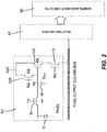
- FIG. 2 there is shown a schematic diagram of a typical pixel 60 of the CMOS image sensor 10.
- the pixel 60 includes a photodiode 70 that receives incident light that is converted into a charge.
- a transfer gate (TG) 80 transfers the charge to a floating diffusion 90 which will convert the charge into a voltage.
- the voltage is sent to an amplifier transistor 100 for buffering the signal amplitude.
- the gain of the amplifier 100 is unity, or one, although other gain factors may be used depending on the desired design.
- the row select transistor 110 receives a signal from the row decoder array 30 (see Fig. 1 ) for enabling the particular row of pixels to pass to the routing matrix 40.
- a reset gate transistor 120 functions to reset and clear the floating diffusion 90 of any residual charge before passing another image signal to the floating diffusion 90.
- FIG. 3 there is shown a schematic diagram of the connections between the array of pixels 20 to the routing matrix 40 and then to a sample and hold array 50.
- Fig. 3 depicts only four sample and hold arrays, although as stated hereinabove, in examples that would not be embodiments of the invention, to increase the speed the number of sample and hold arrays may be increased.
- each of the four colors is routed to a particular sample and hold array sequentially in time in a predetermined order. For example, color one is readout out first by enabling one of four sets of switches. The number of switches in each set is determined by N/4 where N is the number of pixels in each row. In transferring color one, the first set of switches including switches S1, S5, S9 and S13 and etc.
- a corresponding second set of switches are connected to the first set of switches, and in transferring color one, this set of switches are also substantially simultaneously closed (S'1, S'5, S'9 and S'13 and etc) for transferring color one that particular sample and hold circuit 50.
- the number of switches in the set second set is also N/4 where N is the total number of pixels in a row. After completion of the transfer to the sample and hold circuit 50, these two sets of switches are opened (S1, S5, S9, S13, S'1, S'5, S'9, S'13 and etc.).
- the second color is then transferred to a sample and hold array 50 by repeating the above sequence with its corresponding first and second set of switches (S2, S6, S10 and S14 and S'2, S'6, S'10, S'14).
- the process is synchronized so that the first color is transferred before the second color is transferred.
- color three using switches S3, S7, S11, S15 and etc. S'3, S'7, S'11, S'15
- color four using switches S4, S8, S12, S16 and etc. S'4, S'8, S'12, S'16 and etc.
- sample and hold channel 1 is green 1; sample and hold channel 2 (50) contains green 2; sample and hold channel 3 (50) contains red; and sample and hold channel 4 (50) contains blue.
- the color information from the sample and hold channels 50 are output substantially simultaneously so that all the color information (four color channels) for each pixel is received by the subsequent attached off-chip signal processing circuitry at substantially the same time. It is noted that, if there are 8 channels, two sequential color information signals are sent out on each clock cycle to the off-chip processing circuitry. Those skilled in the art will recognize that, as the number of channels is increased, the number of color information signals is accordingly increased as described hereinabove.
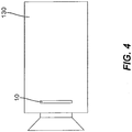
- FIG. 4 there is shown a digital camera 130 containing the image sensor 10 of the present invention for illustrating a typical commercial embodiment of the present invention with which the ordinary consumer is acquainted.
Landscapes
- Engineering & Computer Science (AREA)
- Multimedia (AREA)
- Signal Processing (AREA)
- Transforming Light Signals Into Electric Signals (AREA)
- Color Television Image Signal Generators (AREA)
- Solid State Image Pick-Up Elements (AREA)
Applications Claiming Priority (2)
| Application Number | Priority Date | Filing Date | Title |
|---|---|---|---|
| US11/240,746 US7465934B2 (en) | 2005-09-30 | 2005-09-30 | Pixel array output routing structure for multi-channel CMOS imager sensors |
| PCT/US2006/036252 WO2007040965A1 (en) | 2005-09-30 | 2006-09-18 | Output routing structure for cmos image sensors |
Publications (2)
| Publication Number | Publication Date |
|---|---|
| EP1929789A1 EP1929789A1 (en) | 2008-06-11 |
| EP1929789B1 true EP1929789B1 (en) | 2016-12-14 |
Family
ID=37632496
Family Applications (1)
| Application Number | Title | Priority Date | Filing Date |
|---|---|---|---|
| EP06824985.3A Active EP1929789B1 (en) | 2005-09-30 | 2006-09-18 | Output routing structure for cmos image sensors |
Country Status (7)
| Country | Link |
|---|---|
| US (1) | US7465934B2 (https=) |
| EP (1) | EP1929789B1 (https=) |
| JP (1) | JP4770926B2 (https=) |
| KR (1) | KR101293385B1 (https=) |
| CN (1) | CN101273642B (https=) |
| TW (1) | TWI379597B (https=) |
| WO (1) | WO2007040965A1 (https=) |
Families Citing this family (7)
| Publication number | Priority date | Publication date | Assignee | Title |
|---|---|---|---|---|
| US7593050B2 (en) * | 2006-02-27 | 2009-09-22 | Eastman Kodak Company | Delay management circuit for reading out large S/H arrays |
| US8977578B1 (en) | 2012-06-27 | 2015-03-10 | Hrl Laboratories, Llc | Synaptic time multiplexing neuromorphic network that forms subsets of connections during different time slots |
| TWI497997B (zh) * | 2013-05-17 | 2015-08-21 | Novatek Microelectronics Corp | 影像感測器 |
| FR3091115B1 (fr) | 2018-12-21 | 2021-02-19 | Trixell | Détecteur matriciel à regroupement rapide |
| US11910104B2 (en) | 2019-04-19 | 2024-02-20 | ARIZONA BOARD OF REGENTS on behalf of THE UNIVERSITY OF ARIZONA, A BODY CORPORATE | All-in-focus imager and associated method |
| WO2020215046A1 (en) * | 2019-04-19 | 2020-10-22 | Arizona Board Of Regents On Behalf Of The University Of Arizona | On-chip signal processing method and pixel-array sensor |
| US11428792B2 (en) | 2020-06-08 | 2022-08-30 | Stmicroelectronics (Research & Development) Limited | Routing for DTOF sensors |
Family Cites Families (10)
| Publication number | Priority date | Publication date | Assignee | Title |
|---|---|---|---|---|
| JP3432051B2 (ja) | 1995-08-02 | 2003-07-28 | キヤノン株式会社 | 光電変換装置 |
| US6606122B1 (en) * | 1997-09-29 | 2003-08-12 | California Institute Of Technology | Single chip camera active pixel sensor |
| JP3150098B2 (ja) * | 1998-01-05 | 2001-03-26 | 日本電気アイシーマイコンシステム株式会社 | 液晶駆動装置 |
| US6721008B2 (en) * | 1998-01-22 | 2004-04-13 | Eastman Kodak Company | Integrated CMOS active pixel digital camera |
| US7098952B2 (en) * | 1998-04-16 | 2006-08-29 | Intel Corporation | Imager having multiple storage locations for each pixel sensor |
| US6466265B1 (en) * | 1998-06-22 | 2002-10-15 | Eastman Kodak Company | Parallel output architectures for CMOS active pixel sensors |
| US7068319B2 (en) * | 2002-02-01 | 2006-06-27 | Micron Technology, Inc. | CMOS image sensor with a low-power architecture |
| JP2003284086A (ja) * | 2002-03-27 | 2003-10-03 | Matsushita Electric Ind Co Ltd | 固体撮像装置およびカメラ |
| US20030183829A1 (en) | 2002-03-27 | 2003-10-02 | Matsushita Electric Industrial Co., Ltd. | Solid-state imaging device and camera |
| US7619669B2 (en) | 2003-12-29 | 2009-11-17 | Micron Technologies, Inc. | Power savings with multiple readout circuits |
-
2005
- 2005-09-30 US US11/240,746 patent/US7465934B2/en not_active Expired - Lifetime
-
2006
- 2006-09-18 CN CN2006800357402A patent/CN101273642B/zh active Active
- 2006-09-18 KR KR1020087007662A patent/KR101293385B1/ko active Active
- 2006-09-18 WO PCT/US2006/036252 patent/WO2007040965A1/en not_active Ceased
- 2006-09-18 EP EP06824985.3A patent/EP1929789B1/en active Active
- 2006-09-18 JP JP2008533422A patent/JP4770926B2/ja active Active
- 2006-09-29 TW TW095136338A patent/TWI379597B/zh active
Also Published As
| Publication number | Publication date |
|---|---|
| WO2007040965A1 (en) | 2007-04-12 |
| EP1929789A1 (en) | 2008-06-11 |
| TWI379597B (en) | 2012-12-11 |
| KR20080050456A (ko) | 2008-06-05 |
| CN101273642B (zh) | 2011-08-31 |
| CN101273642A (zh) | 2008-09-24 |
| US7465934B2 (en) | 2008-12-16 |
| JP4770926B2 (ja) | 2011-09-14 |
| TW200746793A (en) | 2007-12-16 |
| JP2009510910A (ja) | 2009-03-12 |
| KR101293385B1 (ko) | 2013-08-05 |
| US20070075255A1 (en) | 2007-04-05 |
Similar Documents
| Publication | Publication Date | Title |
|---|---|---|
| US9131178B2 (en) | Solid-state imaging apparatus for selectively outputting signals from pixels therein | |
| US6466265B1 (en) | Parallel output architectures for CMOS active pixel sensors | |
| EP2323409B1 (en) | Image sensor with charge binning | |
| US6388241B1 (en) | Active pixel color linear sensor with line—packed pixel readout | |
| JP5717561B2 (ja) | イメージセンサのカラム回路およびピクセルビニング回路 | |
| US9380243B2 (en) | Image sensor for outputting RGB bayer signal through internal conversion and image processing apparatus including the same | |
| CN108462841A (zh) | 像素阵列及图像传感器 | |
| KR20050075375A (ko) | 고체촬상장치 | |
| EP1929789B1 (en) | Output routing structure for cmos image sensors | |
| EP1349399A2 (en) | Solid state color image pickup device | |
| JP3956875B2 (ja) | 固体撮像装置 | |
| US7355641B2 (en) | Solid state imaging device reading non-adjacent pixels of the same color | |
| CN216852142U (zh) | 像素阵列和图像传感器 | |
| JP4321008B2 (ja) | 固体撮像素子 | |
| KR100790582B1 (ko) | 씨모스 이미지 센서 픽셀 | |
| JP2003284086A (ja) | 固体撮像装置およびカメラ | |
| JP4765578B2 (ja) | 固体撮像素子とその駆動方法、及びカメラモジュール | |
| JP2004221771A (ja) | 固体撮像装置、カメラおよびカメラシステム | |
| JP2004236028A (ja) | 固体撮像装置、カメラおよびカメラシステム | |
| JP4181421B2 (ja) | 固体撮像装置、カメラおよびカメラシステム | |
| JP2003299111A (ja) | 固体撮像装置及びカメラ | |
| JPS6229386A (ja) | カラ−画像用固体撮像素子 |
Legal Events
| Date | Code | Title | Description |
|---|---|---|---|
| PUAI | Public reference made under article 153(3) epc to a published international application that has entered the european phase |
Free format text: ORIGINAL CODE: 0009012 |
|
| 17P | Request for examination filed |
Effective date: 20080303 |
|
| AK | Designated contracting states |
Kind code of ref document: A1 Designated state(s): DE FR GB NL |
|
| DAX | Request for extension of the european patent (deleted) | ||
| RBV | Designated contracting states (corrected) |
Designated state(s): DE FR GB NL |
|
| RAP1 | Party data changed (applicant data changed or rights of an application transferred) |
Owner name: OMNIVISION TECHNOLOGIES, INC. |
|
| 17Q | First examination report despatched |
Effective date: 20130917 |
|
| REG | Reference to a national code |
Ref country code: DE Ref legal event code: R079 Ref document number: 602006051241 Country of ref document: DE Free format text: PREVIOUS MAIN CLASS: H04N0009040000 Ipc: H04N0005378000 |
|
| GRAP | Despatch of communication of intention to grant a patent |
Free format text: ORIGINAL CODE: EPIDOSNIGR1 |
|
| INTG | Intention to grant announced |
Effective date: 20160630 |
|
| RIC1 | Information provided on ipc code assigned before grant |
Ipc: H04N 5/378 20110101AFI20160620BHEP Ipc: H04N 5/374 20110101ALI20160620BHEP |
|
| GRAS | Grant fee paid |
Free format text: ORIGINAL CODE: EPIDOSNIGR3 |
|
| GRAA | (expected) grant |
Free format text: ORIGINAL CODE: 0009210 |
|
| AK | Designated contracting states |
Kind code of ref document: B1 Designated state(s): DE FR GB NL |
|
| REG | Reference to a national code |
Ref country code: GB Ref legal event code: FG4D |
|
| REG | Reference to a national code |
Ref country code: DE Ref legal event code: R096 Ref document number: 602006051241 Country of ref document: DE |
|
| REG | Reference to a national code |
Ref country code: NL Ref legal event code: FP |
|
| REG | Reference to a national code |
Ref country code: FR Ref legal event code: PLFP Year of fee payment: 12 |
|
| REG | Reference to a national code |
Ref country code: DE Ref legal event code: R097 Ref document number: 602006051241 Country of ref document: DE |
|
| PLBE | No opposition filed within time limit |
Free format text: ORIGINAL CODE: 0009261 |
|
| STAA | Information on the status of an ep patent application or granted ep patent |
Free format text: STATUS: NO OPPOSITION FILED WITHIN TIME LIMIT |
|
| 26N | No opposition filed |
Effective date: 20170915 |
|
| REG | Reference to a national code |
Ref country code: FR Ref legal event code: PLFP Year of fee payment: 13 |
|
| REG | Reference to a national code |
Ref country code: DE Ref legal event code: R079 Ref document number: 602006051241 Country of ref document: DE Free format text: PREVIOUS MAIN CLASS: H04N0005378000 Ipc: H04N0025780000 |
|
| PGFP | Annual fee paid to national office [announced via postgrant information from national office to epo] |
Ref country code: NL Payment date: 20250812 Year of fee payment: 20 |
|
| PGFP | Annual fee paid to national office [announced via postgrant information from national office to epo] |
Ref country code: DE Payment date: 20250808 Year of fee payment: 20 |
|
| PGFP | Annual fee paid to national office [announced via postgrant information from national office to epo] |
Ref country code: GB Payment date: 20250814 Year of fee payment: 20 |
|
| PGFP | Annual fee paid to national office [announced via postgrant information from national office to epo] |
Ref country code: FR Payment date: 20250808 Year of fee payment: 20 |