EP1925040B1 - High temperature superconducting wires and coils - Google Patents
High temperature superconducting wires and coils Download PDFInfo
- Publication number
- EP1925040B1 EP1925040B1 EP06851624.4A EP06851624A EP1925040B1 EP 1925040 B1 EP1925040 B1 EP 1925040B1 EP 06851624 A EP06851624 A EP 06851624A EP 1925040 B1 EP1925040 B1 EP 1925040B1
- Authority
- EP
- European Patent Office
- Prior art keywords
- layer
- superconductor
- wire
- superconducting
- magnetic field
- Prior art date
- Legal status (The legal status is an assumption and is not a legal conclusion. Google has not performed a legal analysis and makes no representation as to the accuracy of the status listed.)
- Active
Links
Images


Classifications
-
- H—ELECTRICITY
- H10—SEMICONDUCTOR DEVICES; ELECTRIC SOLID-STATE DEVICES NOT OTHERWISE PROVIDED FOR
- H10N—ELECTRIC SOLID-STATE DEVICES NOT OTHERWISE PROVIDED FOR
- H10N60/00—Superconducting devices
- H10N60/20—Permanent superconducting devices
- H10N60/203—Permanent superconducting devices comprising high-Tc ceramic materials
-
- H—ELECTRICITY
- H10—SEMICONDUCTOR DEVICES; ELECTRIC SOLID-STATE DEVICES NOT OTHERWISE PROVIDED FOR
- H10N—ELECTRIC SOLID-STATE DEVICES NOT OTHERWISE PROVIDED FOR
- H10N60/00—Superconducting devices
- H10N60/01—Manufacture or treatment
-
- H—ELECTRICITY
- H01—ELECTRIC ELEMENTS
- H01P—WAVEGUIDES; RESONATORS, LINES, OR OTHER DEVICES OF THE WAVEGUIDE TYPE
- H01P1/00—Auxiliary devices
- H01P1/20—Frequency-selective devices, e.g. filters
- H01P1/201—Filters for transverse electromagnetic waves
- H01P1/203—Strip line filters
-
- H—ELECTRICITY
- H01—ELECTRIC ELEMENTS
- H01F—MAGNETS; INDUCTANCES; TRANSFORMERS; SELECTION OF MATERIALS FOR THEIR MAGNETIC PROPERTIES
- H01F41/00—Apparatus or processes specially adapted for manufacturing or assembling magnets, inductances or transformers; Apparatus or processes specially adapted for manufacturing materials characterised by their magnetic properties
- H01F41/02—Apparatus or processes specially adapted for manufacturing or assembling magnets, inductances or transformers; Apparatus or processes specially adapted for manufacturing materials characterised by their magnetic properties for manufacturing cores, coils, or magnets
- H01F41/04—Apparatus or processes specially adapted for manufacturing or assembling magnets, inductances or transformers; Apparatus or processes specially adapted for manufacturing materials characterised by their magnetic properties for manufacturing cores, coils, or magnets for manufacturing coils
- H01F41/048—Superconductive coils
-
- H—ELECTRICITY
- H01—ELECTRIC ELEMENTS
- H01F—MAGNETS; INDUCTANCES; TRANSFORMERS; SELECTION OF MATERIALS FOR THEIR MAGNETIC PROPERTIES
- H01F6/00—Superconducting magnets; Superconducting coils
- H01F6/06—Coils, e.g. winding, insulating, terminating or casing arrangements therefor
-
- Y—GENERAL TAGGING OF NEW TECHNOLOGICAL DEVELOPMENTS; GENERAL TAGGING OF CROSS-SECTIONAL TECHNOLOGIES SPANNING OVER SEVERAL SECTIONS OF THE IPC; TECHNICAL SUBJECTS COVERED BY FORMER USPC CROSS-REFERENCE ART COLLECTIONS [XRACs] AND DIGESTS
- Y02—TECHNOLOGIES OR APPLICATIONS FOR MITIGATION OR ADAPTATION AGAINST CLIMATE CHANGE
- Y02E—REDUCTION OF GREENHOUSE GAS [GHG] EMISSIONS, RELATED TO ENERGY GENERATION, TRANSMISSION OR DISTRIBUTION
- Y02E40/00—Technologies for an efficient electrical power generation, transmission or distribution
- Y02E40/60—Superconducting electric elements or equipment; Power systems integrating superconducting elements or equipment
-
- Y—GENERAL TAGGING OF NEW TECHNOLOGICAL DEVELOPMENTS; GENERAL TAGGING OF CROSS-SECTIONAL TECHNOLOGIES SPANNING OVER SEVERAL SECTIONS OF THE IPC; TECHNICAL SUBJECTS COVERED BY FORMER USPC CROSS-REFERENCE ART COLLECTIONS [XRACs] AND DIGESTS
- Y10—TECHNICAL SUBJECTS COVERED BY FORMER USPC
- Y10S—TECHNICAL SUBJECTS COVERED BY FORMER USPC CROSS-REFERENCE ART COLLECTIONS [XRACs] AND DIGESTS
- Y10S505/00—Superconductor technology: apparatus, material, process
- Y10S505/70—High TC, above 30 k, superconducting device, article, or structured stock
- Y10S505/704—Wire, fiber, or cable
- Y10S505/705—Magnetic coil
-
- Y—GENERAL TAGGING OF NEW TECHNOLOGICAL DEVELOPMENTS; GENERAL TAGGING OF CROSS-SECTIONAL TECHNOLOGIES SPANNING OVER SEVERAL SECTIONS OF THE IPC; TECHNICAL SUBJECTS COVERED BY FORMER USPC CROSS-REFERENCE ART COLLECTIONS [XRACs] AND DIGESTS
- Y10—TECHNICAL SUBJECTS COVERED BY FORMER USPC
- Y10T—TECHNICAL SUBJECTS COVERED BY FORMER US CLASSIFICATION
- Y10T29/00—Metal working
- Y10T29/49—Method of mechanical manufacture
- Y10T29/49002—Electrical device making
- Y10T29/49014—Superconductor
Definitions
- the present invention relates generally to high temperature superconducting wires.
- the invention relates to coated conductors, also called second generation, high temperature superconductor wires or tapes.
- the present invention also relates to superconducting structures that can maintain a constant current in varying magnetic field orientations.
- HTS high-temperature superconducting
- Y123 oxide superconductor including yttrium, barium, copper and oxygen in the well-known basic composition of YBa 2 Cu 3 O 7-X (hereinafter referred to as Y123).
- RE rare earth elements
- HTS wires are the preferred material for many applications, including cables, motors, generators, synchronous condensers, transformers, current limiters, and magnet systems for military, high energy physics, materials processing, transportation and medical uses.
- the current carrying capability of the HTS material is strongly related to its crystalline alignment or texture.
- the oxide superconductor grains typically are aligned with their c axis perpendicular to the plane of the wire surface and the ab plane parallel to the wire surface. Grain boundaries formed by the misalignment of neighboring crystalline HTS grains are known to form an obstacle to superconducting current flow, but this obstacle decreases with the increasing degree of alignment or texture. Therefore to make the material into a commercially viable product, e.g. an HTS wire, the HTS material must maintain a high degree of crystalline alignment or texture over relatively long distances. Otherwise, the superconducting current carrying capacity (critical current density) will be limited.
- HTS materials can be fabricated with a high degree of crystallographic alignment or texture over large areas by growing a thin layer of the material epitaxially on top of a flexible tape-shaped substrate, fabricated so that it has a high degree of crystallographic texture at its surface.
- the crystal alignment of the HTS material grows to match the texture of the substrate.
- the substrate texture provides a template for the epitaxial growth of the crystalline HTS material.
- the substrate provides structural integrity to the HTS layer.
- a substrate can be textured to provide a template that yields an epitaxial HTS layer.
- Materials such as nickel, copper, silver, iron, silver alloys, nickel alloys, iron alloys, stainless steel alloys, and copper alloys can be used, among others.
- the substrate can be textured using a deformation process, such as one involving rolling and recrystallization annealing the substrate.
- a deformation process such as one involving rolling and recrystallization annealing the substrate.
- An example of such a process is the rolling-assisted biaxially textured substrate (RABiTS) process.
- RABiTS rolling-assisted biaxially textured substrate
- One or more buffer layers can be deposited or grown on the substrate surface with suitable crystallographic template on which to grow the HTS material. Buffer layers also can provide the additional benefit of preventing diffusion of atoms from the substrate material into the crystalline lattice of the HTS material or of oxygen into the substrate material. This diffusion, or "poisoning," can disrupt the crystalline alignment and thereby degrade the electrical properties of the HTS material. Buffer layers also can provide enhanced adhesion between the substrate and the HTS layer. Moreover, the buffer layer(s) can have a coefficient of thermal expansion that is well matched to that of the superconductor material. For implementation of the technology in commercial applications, where the wire may be subjected to stress, this feature is desirable because it can help prevent delamination of the HTS layer from the substrate.
- a non-textured substrate such as Hastelloy can be used, and textured buffer layers deposited by means such as the ion-beam-assisted deposition (IBAD) or inclined substrate deposition (ISD). Additional buffer layers may be optionally deposited epitaxially on the IBAD or ISD layer to provide the final template for epitaxial deposition of an HTS layer.
- IBAD ion-beam-assisted deposition
- ISD inclined substrate deposition
- Additional buffer layers may be optionally deposited epitaxially on the IBAD or ISD layer to provide the final template for epitaxial deposition of an HTS layer.
- an HTS layer can be grown epitaxially with excellent crystal alignment or texture, also having good adhesion to the template surface, and with a sufficient barrier to poisoning by atoms from the substrate.
- the HTS layer can be deposited by any of a variety of methods, including the metal-organic deposition (MOD) process, metal-organic chemical vapor deposition (MOCVD), pulsed laser deposition (PLD), thermal or e-beam evaporation, or other appropriate methods.
- MOD metal-organic deposition
- MOCVD metal-organic chemical vapor deposition
- PLD pulsed laser deposition
- thermal or e-beam evaporation thermal or e-beam evaporation, or other appropriate methods.
- a cap layer can be added to the multilayer assembly, which helps prevent contamination of and damage to the HTS layer from above.
- the cap layer can be, e.g., silver, and can be, e.g., sputtered onto the HTS layer.
- HTS wire development continues to seek improvements in critical current density, in particular, critical current density in high magnetic fields and temperatures (J c (H,T)).
- This improvement can come by improving the "pinning" of the superconducting vortices, which is the underlying mechanism for high critical current density J c in HTS materials.
- J c (H,T) critical current density in high magnetic fields and temperatures
- This improvement can come by improving the "pinning" of the superconducting vortices, which is the underlying mechanism for high critical current density J c in HTS materials.
- J c (H,T) critical current density in HTS materials.
- the cross-sectional core has a size on the order of the coherence length, which is several nanometers in high temperature superconducting cuprates and grows with temperature.
- nanometer-sized defects are introduced into the oxide superconductor grains to pin flux lines and improve current carrying properties in a magnetic field.
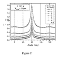
- Figure 1 shows the typical field dependence of a metal-organic deposited (MOD) Y123 film on an oxide-buffered metal substrate with magnetic field oriented parallel and perpendicular to the planar face of the film.
- MOD metal-organic deposited
- Y123 films typically show a small peak in the c-axis (0° and 180° or perpendicular to the planar face of the Y123 film), which can be enhanced through the presence of extended planar or linear defects (e.g., twin boundaries, grain boundaries, a-axis grains).
- HTS wires will experience local variations in the magnetic field orientation, so that the magnetic field experienced in one region of the wire can be quite different from the magnetic field experienced in another wire region.
- the Y123 wire performance is determined by the minimum performance at any magnetic field orientation, and not solely by that at the perpendicular orientation.
- the HTS wire demonstrates reductions in current density in regions where the magnetic field deviates from an optimum orientation.
- the document US-A-2005/007227 describes rare-earth-Ba-Cu-O superconductors having improved critical current density and methods of making same. These superconductors comprise a drop in Jc of less than a factor of about 7 at a temperature of between about 30K to about 77K, and at a magnetic field of about 1 Tesla, when the magnetic field is applied normal to the surface of the superconductor, as compared to a Jc in the presence of no magnetic field.
- US 5428005 discloses a superconducting thin film of compound oxide material deposited on a substrate comprising a plurality of alternatively laminated a-axis or b-axis and c-axis oriented unit layers.
- High temperature superconducting (HTS) wires are described, which may be used in applications and devices experiencing different magnetic field orientations at different locations within the wire or device.
- the HTS wires contain at least two superconducting layers, each of which is selected for its performance at a particular magnetic field orientation. By selecting a combination of superconducting layers, the HTS wire exhibits optimum performance in magnetic fields oriented parallel to the wire surface (H//ab) or, perpendicular to the wire surface (H//c), or at intermediate orientations.
- a superconducting wire includes at least first and second superconducting layers disposed on one or more substrates in stacked relationship.
- the first superconducting layer includes a first high temperature superconducting oxide selected to provide a first predetermined ratio of critical current in a magnetic field parallel to the surface of the superconductor layer to critical current in a magnetic field perpendicular to the surface of the superconductor layer (I c (H//ab)/I c (H///c)), and the second superconducting layer includes a second high temperature superconducting layer selected to provide a second predetermined ratio of critical current in a magnetic field parallel to the surface of the superconductor layer to critical current in a magnetic field perpendicular to the surface of the superconductor layer (I c (H//ab)/I c (H//c)).
- the first and second superconductor layers in combination, provide a predetermined overall critical current Ic in a selected magnetic field orientation.
- the first and second superconducting layers are c-axis oriented and the first superconducting layer is selected to provide a higher critical current in a magnetic field perpendicular to the surface of the superconducting layer than the second superconducting layer and the second superconducting layer is selected to provide a higher critical current in a magnetic field parallel to the surface of the superconducting layer than the first superconducting layer.
- the first predetermined ratio for (I c (H//ab)/I c (H//c)) is less than or equal to 2.6, is less than 2.0, or less than 1.5, in an applied magnetic field of 1 Tesla or greater, e.g., in the range of about 1 Tesla to about 6 Tesla.
- the high temperature superconductor includes a rare earth-alkaline earth-copper oxide including two or more rare earth elements, e.g., one or more of erbium and holmium. Holmium and/or erbium are present in an amount in the range of 25% to 150% of the stoichiometric amount of rare earth in rare earth-alkaline earth-copper oxide.
- the high temperature superconductor includes a rare earth-alkaline earth-copper oxide and at least one second phase nanoparticle comprising a metal-containing compound located within a grain of the oxide superconductor.
- the first or the second high temperature superconductor composition is selected to provide enhanced critical current (Ic) in the presence of magnetic fields oriented parallel to surface of the superconducting layer (H//ab).
- the second predetermined ratio for (I c (H//ab)/I c (H//c)) is greater than 2.5, or greater than 3.5, or greater than 5.5, in an applied magnetic field of 1 Tesla or greater, e.g., in the range of about 1 Tesla to about 6 Tesla.
- the high temperature superconductor includes a rare earth-alkaline earth-copper oxide, wherein the copper to alkaline earth ratio is greater than 1.5.
- the thicknesses of the first and second superconductor layers are different, the thickness of the first and second superconductor layers are selected to provide a predetermined overall critical current in a selected magnetic field orientation. Additional layers that enhance critical current density in magnetic fields either parallel or perpendicular to the surface of the superconductor layer maybe included.
- the selected magnetic field orientation is between 0° (H//c) and 90° (H//ab).
- the superconductor wire includes a first coated element.
- the first coated element includes a first substrate, at least one first buffer layer disposed on the first substrate and supporting the first superconducting layer, and a first metallic protective layer disposed on the first superconductor layer.
- the second coated element includes a second substrate, at least one second buffer layer disposed on the second substrate and supporting the second superconducting layer, and a second metallic protective layer disposed on the second superconductor layer.
- the superconducting wire also includes an intervening binder layer disposed between the first and second coated elements such that the first and second coated elements are joined at the first and second substrates, or an intervening binder layer disposed between the first and second coated elements such that the first and second coated elements are joined at the first and second metallic protective layers.
- the method which does not form part of the present invention includes providing a length of superconducting wire comprising a first region comprising a high Ic(H//c) high temperature superconductor composition, a second region comprising of a high Ic(H//ab) high temperature superconductor composition, and a third region comprising a mixture of the high Ic(H//c) high temperature superconductor composition and the high Ic(H//ab) high temperature superconductor composition, and arranging the length of superconductor in the device such that the first region occupies a location in the device experiencing a magnetic field orientation perpendicular (0°) to the high temperature wire, the second region occupies a location in the device experiencing a magnetic field orientation parallel (90°) to the high temperature wire, and the third region occupies a location in the device experiencing a magnetic field orientation between 0° and 90°.
- the device may be a coil; the first region of the high temperature superconductor wire is positioned at the ends of the coil; the second region of the high temperature superconductor wire is positioned in the interior of the coil; and the third region of the high temperature superconductor wire is positioned between the first and second regions.
- an article includes a superconducting wire comprising a high temperature superconductor layer, wherein the article experiences a magnetic field of differing orientation at different locations in the article, and wherein the composition of the high temperature superconductor layer is varied along its length to accommodate the orientation of the magnetic field in a given location.
- the article which does not form part of the present invention. is a coil and, in operation, the coil experiences induced magnetic fields that range from substantially parallel to the plane of the superconductor layer to substantial perpendicular to the plane of the superconductor layer.
- the composition of the superconductor wire is primarily a high I c (H//c) high temperature superconductor composition in a first region of the coil that experiences magnetic fields perpendicular to surface of the superconducting layer during operation; the composition of the superconductor wire comprises primarily a high I c (H//ab) high temperature superconductor composition in a second region of the coil that experiences magnetic fields that are substantially parallel to surface of the superconducting layer during operation; and the composition of the superconductor wire comprises a mixture of a high I c (H//c) high temperature superconductor composition and a high I c (H//ab) high temperature superconductor composition in a region of the coil that experiences magnetic fields that are at an angle of between 0 and 90 degrees to surface of the superconducting layer during operation.
- stacked relationship it is meant that the elements are arranged in a stack, e.g., in overlaying relationship to one another wherein the layers may be in contact or they may have one or more intervening layers between them. No stacking order is suggested or implied.
- Figure 3 shows a two-dimensional plot of the magnetic field distribution around the end turns 300 of a solenoid electromagnet 310, which demonstrates that both the field strength (H) (designated in arrows of different colors, where the colors correspond to the field strengths shown in the side bar of Figure 3 ) and field orientation ( ⁇ ) (designated by arrow orientation) vary dramatically at different locations in the coil.
- An HTS wire that is optimized for electrical current carrying properties in a particular magnetic field will exhibit different currents (Ic), and hence different current densities (Jc), in different regions of the coil as each region of the coil experiences a magnetic field of different orientation.
- the performance of the coil is limited by the minimum performance of the wire.
- the overall current of the wire is reduced throughout and the wire functions at only a fraction of its current capacity over long lengths of the wire. If the current capacity can be increased for those underperforming regions of the wire, the current of the entire wire as a whole can be improved.
- RE123 superconducting oxide grains typically exhibit strong anisotropy in a magnetic field, with the current in a magnetic field oriented in the (ab) plane of the oxide grain (along the surface of an epitaxial HTS layer) being much higher than the current in a magnetic field oriented perpendicular to the HTS layer, I c (H//ab) can be two times, three times, and even more than ten times greater than I c (H//c); and the anisotropy becomes more noted at higher magnetic field strength. While certain HTS materials have been observed to reduce magnetic field anisotropy, improvements in I c (H//c) are typically obtained at the expense of I c (H//ab).
- an HTS wire operates at higher percentage of the total current capacity than a conventional HTS wire.
- the HTS wire operates at near full current load.
- Current carrying characteristics are improved by using HTS materials with different performance characteristics in different regions of an HTS wire or device.
- the HTS material is selected for optimal performance in the anticipated local magnetic field orientation.
- an HTS wire includes two superconducting layers that are selected to provide optimal performance in the local applied magnetic field. The two layers may be arranged or stacked in any order.
- both layers may contain a superconductor layer having a composition and structure that provides optimal current along H//ab, that is, I c (H//ab)» I c (H//c).
- both layers may contain a superconductor layer having a composition and structure that provides optimal current along H//c, that is, the Ic anisotropy is reduced to a desired level.
- a first layer contains a superconductor layer having a composition and structure that provides optimal current performance along H//ab
- a second layer contains a superconductor layer having a composition and structure that provides optimal current along Hllc.
- the relative thickness of the two layers is selected to provide the desired balance of I c (H//c) and I c (H//ab) performance.
- the HTS wires provide an overall critical current of a desired performance, e.g., a desired current load.
- the HTS wire carries an overall I c (H//c) in at least a portion of its length of at least 80A/cm-width; and I c (H//ab)/ I c (H//c) is greater than 2.0, or about 2-3; or I c (H//c) is about 120-150 A/cm-width and I c (H//ab)/ I c (H//c) is greater than 2.0 or about 2-3; or I c (H//c) is about 150-180 A/cm-width and I c (H//ab)/ I c (H//c) is greater than 2.0, or about 2-3.
- the overall I c (H//c) is attained by the additive current performance of the two superconducting layers. Specifying a high I c (H//c) ensures that at least one of the layers performs well in a perpendicular magnetic field. Specifying that I c (H//ab) be a multiple of Il c (H//c) of 2 or more ensures that current in a parallel field is even higher.
- the overall current performance may be attained in a variety of combinations, such as combining two wires having moderate I c (H//c) and moderate I c (H//ab). Alternatively, a wire of superior I c (H//c) can be combined with a wire of poor I c (H//c), but good I c (H//ab).
- the two layer HTS wires increase critical current density over comparable single layer superconductor wires by substantially doubling the volume of superconductor material in the HTS wire.
- the superconducting layers may be coated on the same side of the substrate.
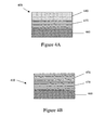
- Figure 4A illustrates a double layer HTS wire 400 in which one superconducting layer having optimal I c (H//ab) 440 and one superconducting layer having optimal I c (H//c) 470 are coated on the same side of the substrate 460. It should be noted that in this and all subsequent figures, the dimensions are not to scale.
- the substrate may be a textured metal substrate or a metal substrate that includes a textured substrate and is generally of a thickness in the range of about 0.05 - 0.2 mm.
- a metal substrate such as Ni, Ag, or Ni alloys (e.g., NiW or other Hastalloy metals) provides flexibility for the wire and can be fabricated over long lengths and large areas.
- the superconducting layer comprises a material that is selected for its good performance in either H//ab or H//c.
- the superconductor layer is crystallographically aligned so that the ab plane of the oxide superconductor is parallel to the wire surface.
- Each superconducting layer is generally in the range of about 0.5 ⁇ m to about 2.0 ⁇ m, and may be even greater.
- An HTS wire as illustrated in Figure 4A is typically useful in a wire or region of a wire experiencing a magnetic field of intermediate orientation, that is, 0° ⁇ ⁇ ⁇ 90°.
- a double layer HTS wire 410 not according to the present invention in which two superconducting layers 470 having optimal I c (H//c) are coated on the same side of the substrate 460 may be used, as Figure 4B illustrates.
- Figure 4C illustrates a double layer HTS wire 420 not according to the present invention, in which two superconducting layers having optimal I c (H//ab) 440 are coated on the same side of the substrate 460.
- the HTS layer demonstrates an optimal performance in H//ab.
- a wire may include any one of these architectures at different locations in the device corresponding to different field orientations.
- a conducting or insulating layer 490 may be disposed between the first and second superconductor layers as illustrated for HTS wire 430 in Figure 4D .
- Conductor layers provide electrical connection between the two layers and can be, for example, copper, and silver.
- Exemplary insulating layers include metal oxides such as Y 2 O 3 , CuO and CeO 2 .
- Any interlayer should be structurally and chemically compatible with the HTS material and have, for example, a textured crystalline structure that permits the deposition of an epitaxial HTS layer.
- the interlayer thickness is generally in the range of 20 nm to 200 nm, and is deposited, for example, by sputtering, evaporation deposition or pulsed vapor deposition, or other conventional methods.
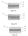
- the superconductor layers are coated on opposite sides of the substrate.
- Figure 5A illustrates a double layer HTS wire 520 in which one superconducting layer having optimal I c (H//ab) 440 and one superconducting layer having optimal I c (H//c) 470 are coated on opposite sides of the substrate 460.
- Figure 5B illustrates a double layer HTS wire 510 not according to the present invention, in which two superconducting layers 470 having optimal I c (H//c) are coated on opposite sides of the substrate 460.
- Figure 5C illustrates a double layer HTS wire 500 not according to the present invention, in which two superconducting layers having optimal I c (H//ab) 440 are coated on opposite sides of the substrate. Additional superconducting layers may be included on either side of the substrate and may enhance either I c (H//c) or I c (H//ab).
- the HTS wires illustrated in Figures 4A-4D and Figures 5A-5C and elsewhere in this description include one or more buffer layers (not shown) disposed between the substrate and superconductor layer and one or more cap layers (not shown) overlaying the superconductor.
- the buffer layer is made up of an electrically insulating material, though electrically conductive materials also can be used.
- the buffer layer is made up of, e.g., an inert metal, an oxide, zirconate, titanate, niobate, nitride, tantalate, aluminate, cuprate, manganate, or ruthenate of a metal or rare earth element (e.g.
- the buffer layers may be deposited using any known method, including physical and chemical deposition methods.
- a cap layer overlays the superconducting layer and provides protection of the superconducting layer from chemical and mechanical degradation.
- the cap layer may be conductive.
- the cap layer may be sputtered Ag or other inert metal.
- superconducting materials having high I c (H//ab) or high I c (H//c) are obtained by selective processing of the layers.
- this can be accomplished by changing the processing conditions used to form the superconductor during the process.
- reaction to form the superconductor is initiated at the interface with the underlying buffer layer and the superconductor grows from that interface outward.
- changing conditions midway in the process from those that favor a high I c (H//c) material to those that favor a high I c (H//ab) material results in a layered structure with different current carrying properties.
- the two superconductor layers can be separately processed to optimize performance and joined after HTS formation.
- Exemplary superconducting materials having good performance in H//ab include rare earth (RE)-alkaline earth-copper oxides in which the metals are substantially in stoichiometric proportions.
- RE-123 in which the rare earth, barium and copper are in substantially 1:2:3 proportions have been found to exhibit optimal current in magnetic fields oriented parallel to the ab plane.
- An exemplary oxide superconductor is YBa 2 Cu 3 O 7- ⁇ .
- the superconducting oxide is a rare earth barium copper oxide in which the copper to barium ratio is greater than 1.5.
- the Cu:Ba ratio is achieved by reducing the amount of barium in the oxide superconductor, i.e., the proportion of barium is less than 2.0, or by increasing the copper content, i.e., the proportion of copper is greater than 3.0, in the RE-123 composition.
- the oxide superconductor contains an excess of copper, for example, up to 5% excess, or up to 10% excess or up to 20% excess copper as compared to the amount of copper required to prepare stoichiometric RE-123.
- the oxide superconductor contains an deficiency of barium, for example, up to 5% deficiency, or up to 10% deficiency or up to 20% deficiency of barium as compared to the amount of copper required to prepare stoichiometric RE-123.
- a copper interlayer is used in whole or in part to supply excess copper.
- a copper layer is deposited as an interlayer in between two superconductor layers in a double layer wire, as in Figures 4A-4D .
- copper diffuses into both superconductor layers 440, 470, forming copper-rich HTS layers.
- Further information on the use of copper interlayers in the processing of copper-rich HTS wires is found in co-pending and commonly owned United States Patent Publication No. 2006-0094603, published on May 4, 2006 , and entitled "Thick Superconductor Films With Improved Performance,".
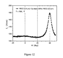
- FIG. 6 is a plot of critical current (Ic) versus magnetic field orientation ( ⁇ ), 75K) for oxide superconductors of various compositions. Curves 610 and 610' measure the current over a range of ⁇ at 1T and 3T, respectively, for a Y-123 layer containing 7.5% excess copper. The curves exhibit a strong maximum at 90° (H//ab) and a minimum at 0° (H//c), thus demonstrating the optimal performance of this superconductor composition at H//ab.
- Copper-rich Y-123 also exhibits a strong current anisotropy between H//ab and H//c, where the ratio of I c (H//ab) to I c (H//c) is about 2.4 at 1T and 6 at 3T.
- a high I c (H//c) superconductor has an Ic(H//c) of greater 20-55 A/cm-width 65K at 3T and an I c (H//ab)/ I c (H//c) ratio greater than 2.5, or greater than 3.5 or greater than 5.5 in a magnetic field of at least 1 Tesla. Such ratios have been obtained for magnetic field strengths of up to 6 Tesla and it is anticipated that such ratios may be appropriate in even higher magnetic fields.
- Exemplary superconducting materials having good performance in H//c include rare earth (RE)-alkaline earth-copper oxides containing an excess of rare earth element or two or more rare earth elements in stoichiometric proportions or in excess of stoichiometric proportions. Without being bound by any particular mode of operation, the excess rare earth is believed to improve I c (H//c) by forming nanoscale defects that serve as flux pinning centers. Atomistic defects may be achieved by introducing different rare earth elements into the Y-123 superconductor. In one or more embodiments, up to about 25% addition to, for example, a yttrium-containing composition, or up to about 150% substitution of a rare earth element is contemplated.
- RE rare earth
- the rare earth element is holmium and/or erbium.
- Introduction of two or more rare earths into the oxide superconductor layer not only increases I c (H//c), but it also decreases the difference (anisotropy) between I c (H//ab) and I c (H//c).
- the critical current at 90° (H//ab) has decreased significantly, while the critical current at 0° (H//c) has increased, thus demonstrating that the composition of the superconducting layers can be selected to improve the critical current at H//c, in absolute terms, as well as to reduce the current anisotropy between I c (H//ab) and I c (H//c).
- the ratio of I c (H//ab) to I c (H//c) for the 25% erbium-supplemented Y-123 is about 1.8 at 1 T and 2.6 at 3T, while the ratio of H//ab to H//c for the 50% erbium-supplemented Y-123 is about 1.2 at 1 T and 1.6 at 3T. This is considerably less than the current anisotropy of a high I c (H//ab) wire. Compare, I c (H//ab)/ I c (H//c) of 2.4 (1T) and 6.0 (3T) for copper-rich Y-123.
- a high I c (H//c) superconductor layer has an I c (H//ab)/ I c (H//c) ratio of less than 2.6, or less than 2.0 or less than 1.5 in a magnetic field of at least 1 Tesla.
- I c (H//ab)/ I c (H//c) ratio of less than 2.6, or less than 2.0 or less than 1.5 in a magnetic field of at least 1 Tesla.
- the high I c (H//c) superconductor material includes a second phase nanoparticle within the grain of the oxide superconductor.
- the nanoparticle is made up of a metal-containing compound and may contain one or more of rare earth element, an alkaline earth metal, and a transition metal.
- the second phase nanoparticle may be one or more of zirconium oxide, aluminum oxide, Y 2 Cu 2 O 5 , YaBaCuO 4 , magnesium oxide, BaZr ⁇ 3, silver and Ce ⁇ 2.
- Other compositions suitable for forming nanometer-sized defects in the oxide superconductor grains to pin flux lines and improve current carrying properties in a magnetic field are found in co-pending and commonly owned application United States Serial No. 10/758,710, filed January 16, 2005 , and entitled "Oxide Films with Nanodot Flux Pinning Centers,".
- the thickness of the high I c (H//ab) and high I c (H//c) layers may be selected to provide a preselected performance in a magnetic field orientation.
- a high I c (H//c) superconductor layer and a high I c (H//ab) superconductor layer, where the I c (H//c) layer is thinner relative to the I c (H//ab) layer based on data such as is presented in Figure 6 .
- the relative thickness of the two layers can be adjusted to obtain, for example, I c (H//c) > 80 A/cm-width and I c (H//ab)/ I c (H//c) of greater than 2, or I c (H//c) > 120-150 A/cm-width and I c (H//ab)/ I c (H//c) of greater than 2, or I c (H//c) > 150-180 A/cm-width and I c (H//ab)/ I c (H//c) of 2-3.
- the superconductor layers are deposited by metal organic deposition (MOD).
- MOD metal organic deposition
- a precursor solution containing the constituent elements of the first oxide superconductor layer is deposited and the precursor layer is decomposed into an intermediate metaloxy layer before application of the second superconductor layer.
- a second precursor solution containing the constituent metallic elements of the second oxide superconductor layer is then deposited and decomposed into an intermediate metaloxy layer.
- the two intermediate layers are then fully converted into an HTS layer.
- the precursor solutions may include metal salts including fluoride, and the precursor may be decomposed to form an intermediate metal oxyfluoride layer.
- the metal oxyfluoride layer may be further heat treated to form an oxide superconductor.
- the first precursor layer is deposited and fully converted into an oxide superconductor layer.
- the second precursor layer is then deposited and also fully converted into an oxide superconductor layer.
- Each superconductor layer can be a thickness of about 0.6 ⁇ m to about 1.5 ⁇ m, or even greater.
- the total thickness of the superconducting layers can range from about 0.6 ⁇ m to about 2.0 ⁇ m and generally does not exceed about 3 ⁇ m.
- each superconducting layer is deposited on a separate substrate, i.e., an HTS assembly.
- the coated substrates are then joined to form an HTS wire containing two substrate/superconductor layer assemblies.
- HTS assembly indicates a multilayer structure including a substrate, one or more buffer layers, a superconductor layer, and one or more cap layers.
- HTS wire 700 is made up of two HTS assemblies 710 and 720. Each of these assemblies is fabricated using techniques known in the art and that are described in greater detail herein.
- Assembly 710 includes a metal substrate 760.
- Substrate 760 contains at least a biaxially textured surface to provide a crystal template for buffer layer 750 and HTS layer 740.
- Buffer layer 750 overlays substrate 760 and may comprise one or more layers.
- HTS layer 740 overlays buffer layer 750 may be any HTS material.
- the HTS layer includes a rare earth-alkaline earth-copper oxide, such as Y-123, that is optimized for performance in either H//ab or H//c.
- Cap layer 730 is located above HTS layer 740 and provides protection of the HTS layer from chemical and mechanical degradation.
- Insert 720' may have the identical or similar structure, including substrate 760', buffer layer 750', HTS layer 740', and cap layer 730'.
- superconductor layer 740 is shown as a high I c (H//c) superconductor material and superconductor layer 740' is shown as a high I c (H//ab) material.
- Adhesive 780 bonds assembly 710 to assembly 720 at their respective substrates, creating HTS assembly 700.
- Cap layers 730 and 730' face outward in assembly 700, and substrates 760 and 760' are internally located in assembly 700. This configuration provides, for example, efficient electrical contact with an external current source and efficient joining of lengths of superconductor wire.
- the outer surfaces of the assembly are electrically conductive cap layers 730 and 730'. These layers provide convenient electrically conductive paths to respective HTS layers 740 and 740'. In order to introduce current into the HTS layers, a connection between the current source and the assembly can be made anywhere on the outer surface of the assembly.
- wetting layers e.g., Ag or Cu
- adhesive layer 780 is made of solder, a resin, epoxy, or other nonconductive material.
- An exemplary solder is Pb-Sn-Ag.
- the electrically insulating native oxide layers on substrates 760 and 760' may be first removed. This removal can be done, e.g., by etching, electro-polishing, sputtering, or shot blasting. Then metallic wetting layers, e.g., Ag or Cu, are coated onto the respective back surfaces of substrates 760 and 760' to prevent the regrowth of the native oxide on the substrate surfaces. Rigorous removal of the native oxide layer is not required, however, in order to provide an HTS wire according to one or more embodiments of the present invention. Further detail on HTS assemblies for use in one or more embodiments of the present invention may be found in co-pending and commonly owned U.S. Patent Application No. 11/193,262, filed on July 29, 2005 , and entitled "Architecture For High Temperature Superconductor Wire,".
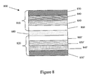
- HTS wire 800 is made up of two HTS assemblies 810 and 820. Each of these assemblies is fabricated using techniques known in the art and is described in greater detail below.
- Assembly 810 includes a metal substrate 830.
- Substrate 830 contains at least a biaxially textured surface to provide a crystal template for buffer layer 840 and HTS layer 850.
- Buffer layer 840 overlays substrate 830 and may comprise one or more layers.
- HTS layer 850 overlays buffer layer 840 may be any HTS material.
- the HTS layer includes a rare earth-alkaline earth-copper oxide, such as Y-123, that is optimized for performance at either H//ab or H//c.
- Cap layer 860 is located above HTS layer 850 and provides protection of the HTS layer from chemical and mechanical degradation.
- Insert 820 may have the identical or similar structure, including substrate 830', buffer layer 840', HTS layer 850', and cap layer 860'.
- superconductor layer 840 is shown as a high I c (H//c) superconductor material and superconductor layer 840' is shown as a high I c (H//ab) material.
- the individual HTS assemblies are joined at cap layers 860, 860' using one of a variety of methods.
- exemplary joining techniques include soldering and diffusion bonding.
- An exemplary solder layer 880 is shown in Figure 8 joining the two HTS assemblies 810, 820. Further information regarding HTS assemblies is found in commonly owned U.S. Patent No. 6,828,507 .
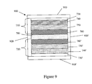
- the electrical stability of the two superconductor layer HTS wires is further enhanced by surrounding the superconductor wire, e.g., such as the wire shown in Figures 7 and 8 , with an electrically conductive structure 900, as is illustrated in Figure 9 .
- the electrically conductive structure allows current transport from one superconductor layer to another. This provides a redundant current path, thereby improving the stability of the wire to quenching and reducing the sensitivity of the wire to local defects and variations in performance.
- the electrically conductive structure may include upper and lower conductive strips 910, 910' in electrical contact with HTS assemblies 710 and 720.
- a substantially nonporous electrically conductive filler 920, 920' extends between the first and second conductive strips along the sides of the superconductor wire assembly to isolate the HTS assemblies from the environment and to provide electrical connectivity between the two superconductor layers and to an external electrical connection.
- filler 920, 920' provides electrical communication between the HTS assemblies 710, 720.
- filler 920, 920' behaves as a conductive conduit, or bridge.
- filler 920, 920' is conductive, as current flows through wire 900, the current will generally follow the path of least resistance, which is through one or both HTS assemblies 710, 720.
- the presence of redundant electrical pathways for the current improves the electrical stability of the wire and increases the current-carrying capacity of wire 900 over that of a single assembly or two isolated assemblies.
- filler 920, 920' provides a means to introduce electrical current into one or both of HTS assemblies 710, 720.
- Material 920, 920' is selected such that it is nonporous, has sufficient strength and is coatable to a sufficient thickness to substantially surround and seal wire 900.
- the thick coating of filler 920, 920' on the sides of wire 900 also adds mechanical strength to the wire and may help to prevent delamination of wire 900 due to bending or other sources of potential damage.
- Material 920, 920' adds thermal stability to the wire by providing additional heat capacity.
- the wire has sufficient filler width to meet the mechanical strength and durability requirements of wire 900, but not much more.
- a typical individual filler width ranges from 0.025-0.2 mm, but can be higher or lower (e.g. 0.005-1 mm).
- Stabilizer strips 910 and 910' further enhance the mechanical, electrical, and thermal stability of wire 900.
- Strips 910, 910' can be the same or different, depending upon the desired characteristics of the resulting wire.
- the thickness of the strips can be varied throughout a wide range of about 0.01 -2 mm, depending upon the desired application, e.g., between 0.05-0.075 mm, to as high as or higher than 1 mm.
- Strips 910 and 910' are generally a flexible conductive material, e.g. metal, e.g. aluminum, copper, silver, nickel, iron, stainless steel, aluminum alloy, copper alloy, silver alloy, nickel alloy, nickel tungsten alloy, or iron alloy.
- a high conductivity metal such as copper is preferred.
- a mechanically strong, high resistivity alloy such as stainless steel is preferred.
- stabilizer strips 910 and 910' have a width that is greater than the width of HTS assemblies 710 and 720. This excess width, or overhang, allows layers or fillets of filler 920, 920' to form along the sides of the wire by capillary action. Generally, the width of strips 910, 910' fall within the range of 0.01-2 mm greater than the width of HTS assemblies 710, 720. For example, stabilizer strips with a width of about 4.3 mm can be used with 4.0 or 4.1 mm wide superconducting inserts.
- HTS wire e.g., wire 1000 may be manufactured as illustrated in FIG. 10 .
- HTS wire assemblies are fabricated as wide (e.g. about 4 to 10 cm wide) multilayer strips and then slit lengthwise into several narrow (e.g. about 10 strips of about 0.4 cm wide, from a 4 cm wide strip) strips, which form HTS assemblies 1010, 1020. See Step 1190 of Figure 11 .
- Conductive stabilizer strips 1060, 1060' may be wider than the width of the narrow HTS strip, so that the stabilizer strips overhang the HTS strip on both sides.
- the wire is formed by joining narrow HTS insert strips 1010, 1020 with stabilizer strips 1060, 1060' in a bath 1000 of filler material.
- Multilayer HTS inserts 1010, 1020 may be fed into the filler bath from reels 1010, 1010'.
- Stabilizer strips 1060, 1060' may be fed off reels 1020, 1020' placed above and below the feed-in reels 1010, 1010' of HTS 1010, 1020 so that the lengths of material form a stacked configuration.
- the filler simultaneously surrounds and HTS assemblies 1010, 1020 and also laminates them to the conductive stabilizer strips 1060, 1060'.
- Die 1030 merges and consolidates inserts 1010, 1020 and stabilizer strips 1060, 1060' into one superconducting wire 1000.
- the stabilizer strips By laminating the stabilizer strips to the wire after fabricating and slitting the HTS inserts, the stabilizer strips can easily be made wider than the inserts.
- the overhanging feature promotes the capillary wicking of the solder between the upper and lower stabilizer strips 1060, 1060' to provide thick, mechanically robust fillets of filler on the sides of the wire.
- Wires having different performance characteristics can be joined end-to-end to obtain an HTS wire that varies in performance along its length. This is facilitated by use of the HTS wires having an electrically conductive outer structure that provides electrical contact with the oxide superconductor layer, such as is illustrated in Figure 9 .
- HTS wires such as described herein may be used in electromagnetic coils or windings.
- the HTS wire is wound to form a coil such that the HTS wire in the region of the coil experiencing a magnetic field with a strong H//ab component is made up of HTS wire having a high I c (H//ab).
- the HTS wire in the region of the coil experiencing a magnetic field with a strong H//c component is made up of HTS wire having a high I c (H//c) and optionally, a desired ratio I c (H//ab)/ I c (H//c).
- Regions of the coil experiencing magnetic field of intermediate orientation are made up from HTS wires having a desired combination of high I c (H//ab) and high I c (H//c) superconducting layers to obtain a desired I c (H//c) and optionally, a desired ratio I c (H//ab)/ I c (H//c).
- the thicknesses of the two layers may be selected to obtain the desired combination of current density parallel to and perpendicular to the tape surface.
- Fig. 11 illustrates a flow diagram of an exemplary process used to manufacture an HTS wire according to various embodiments of the present invention.
- a wire substrate is treated to obtain biaxial texture.
- the substrate surface has a relatively well defined crystallographic orientation.
- the surface can be a biaxially textured surface (e.g., a (113)[211] surface) or a cube textured surface (e.g., a (100)[011] surface or a (100)[001] surface).
- the peaks in an X-ray diffraction pole figure of the surface have a FWHM of less than about 20° (e.g., less than about 15°, less than about 10°, or from about 5° to about 10°).
- the surface can be prepared, for example, by rolling and annealing.
- Surfaces can also be prepared using vacuum processes, such as ion beam assisted deposition, inclined substrate deposition and other vacuum techniques known in the art to form a biaxially textured surface on, for example, a randomly oriented polycrystalline or amorphous surface.
- the surface of the substrate need not be textured (e.g., the surface can be randomly oriented polycrystalline, or the surface can be amorphous).
- the substrate can be formed of any material capable of supporting a buffer layer stack and/or a layer of superconductor material, and capable of providing the mechanical properties required for the final wire.
- substrate materials that can be used as the substrate include for example, metals and/or alloys, such as nickel, silver, copper, zinc, aluminum, iron, chromium, vanadium, palladium, molybdenum and/or their alloys.
- the substrate can be formed of a superalloy.
- the substrate can be in the form of an object having a relatively large surface area (e.g., a wire or a wafer). In these embodiments, the substrate is preferably formed of a relatively flexible material.
- the substrate is a binary alloy that contains two of the following metals: copper, nickel, chromium, vanadium, aluminum, silver, iron, palladium, molybdenum, tungsten, gold and zinc.
- a binary alloy can be formed of nickel and chromium (e.g., nickel and at most 20 atomic percent chromium, nickel and from about five to about 18 atomic percent chromium, or nickel and from about 10 to about 15 atomic percent chromium).
- a binary alloy can be formed of nickel and copper (e.g., copper and from about five to about 45 atomic percent nickel, copper and from about 10 to about 40 atomic percent nickel, or copper and from about 25 to about 35 atomic percent nickel).
- a binary alloy can contain nickel and tungsten (e.g., from about one atomic percent tungsten to about 20 atomic percent tungsten, from about two atomic percent tungsten to about 10 atomic percent tungsten, from about three atomic percent tungsten to about seven atomic percent tungsten, about five atomic percent tungsten).
- a binary alloy can further include relatively small amounts of impurities (e.g., less than about 0.1 atomic percent of impurities, less than about 0.01 atomic percent of impurities, or less than about 0.005 atomic percent of impurities).
- Ni-5wt.%W is a preferred material for the substrate.
- the substrate contains more than two metals (e.g., a ternary alloy or a quarternary alloy).
- the alloy can contain one or more oxide formers (e.g., Mg, Al, Mo, V, Ta, Ti, Cr, Ga, Ge, Zr, Hf, Y, Si, Pr, Eu, Gd, Tb, Dy, Ho, Lu, Th, Er, Tm, Be, Ce, Nd, Sm, Yb and/or La, with Al being the preferred oxide former), as well as two of the following metals: copper, nickel, chromium, tungsten, vanadium, aluminum, silver, iron, palladium, molybdenum, gold and zinc.
- oxide formers e.g., Mg, Al, Mo, V, Ta, Ti, Cr, Ga, Ge, Zr, Hf, Y, Si, Pr, Eu, Gd, Tb, Dy, Ho, Lu, Th, Er, Tm, Be, Ce, Nd, Sm, Yb and/or La,
- the alloy can contain two of the following metals: copper, nickel, chromium, tungsten, vanadium, aluminum, silver, iron, palladium, molybdenum, gold and zinc, and can be substantially devoid of any of the aforementioned oxide formers.
- the alloys can contain at least about 0.5 atomic percent oxide former (e.g., at least about one atomic percent oxide former, or at least about two atomic percent oxide former) and at most about 25 atomic percent oxide former (e.g., at most about 10 atomic percent oxide former, or at most about four atomic percent oxide former).
- the alloy can include an oxide former (e.g., at least about 0.5 aluminum), from about 25 atomic percent to about 55 atomic percent nickel (e.g., from about 35 atomic percent to about 55 atomic percent nickel, or from about 40 atomic percent to about 55 atomic percent nickel) with the balance being copper.
- the alloy can include an oxide former (e.g., at least about 0.5 atomic aluminum), from about five atomic percent to about 20 atomic percent chromium (e.g., from about 10 atomic percent to about 18 atomic percent chromium, or from about 10 atomic percent to about 15 atomic percent chromium) with the balance being nickel.
- the alloys can include relatively small amounts of additional metals (e.g., less than about 0.1 atomic percent of additional metals, less than about 0.01 atomic percent of additional metals, or less than about 0.005 atomic percent of additional metals).
- a substrate formed of an alloy can be produced by, for example, combining the constituents in powder form, melting and cooling or, for example, by diffusing the powder constituents together in solid state.
- the alloy can then be formed by deformation texturing (e.g., annealing and rolling, swaging, extrusion and/or drawing) to form a textured surface (e.g., biaxially textured or cube textured).
- deformation texturing e.g., annealing and rolling, swaging, extrusion and/or drawing
- the alloy constituents can be stacked in a jelly roll configuration, and then deformation textured.
- a material with a relatively low coefficient of thermal expansion e.g., Nb, Mo, Ta, V, Cr, Zr, Pd, Sb, NbTi, an intermetallic such as NiAl or Ni 3 Al, or mixtures thereof
- a material with a relatively low coefficient of thermal expansion e.g., Nb, Mo, Ta, V, Cr, Zr, Pd, Sb, NbTi, an intermetallic such as NiAl or Ni 3 Al, or mixtures thereof
- an intermetallic such as NiAl or Ni 3 Al, or mixtures thereof
- stable oxide formation at the surface can be mitigated until a first epitaxial (for example, buffer) layer is formed on the biaxially textured alloy surface, using an intermediate layer disposed on the surface of the substrate.
- Intermediate layers include those epitaxial metal or alloy layers that do not form surface oxides when exposed to conditions as established by PO 2 and temperature required for the initial growth of epitaxial buffer layer films.
- the buffer layer acts as a barrier to prevent substrate element(s) from migrating to the surface of the intermediate layer and forming oxides during the initial growth of the epitaxial layer. Absent such an intermediate layer, one or more elements in the substrate would be expected to form thermodynamically stable oxide(s) at the substrate surface which could significantly impede the deposition of epitaxial layers due to, for example, lack of texture in this oxide layer.
- Exemplary intermediate metal layers include nickel, gold, silver, palladium, and alloys thereof. Additional metals or alloys may include alloys of nickel and/or copper.
- Epitaxial films or layers deposited on an intermediate layer can include metal oxides, chalcogenides, halides, and nitrides. In some embodiments, the intermediate metal layer does not oxidize under epitaxial film deposition conditions.
- the deposited intermediate layer is not completely incorporated into or does not completely diffuse into the substrate before nucleation and growth of the initial buffer layer structure causes the epitaxial layer to be established. This means that after selecting the metal (or alloy) for proper attributes such as diffusion constant in the substrate alloy, thermodynamic stability against oxidation under practical epitaxial buffer layer growth conditions and lattice matching with the epitaxial layer, the thickness of the deposited metal layer has to be adapted to the epitaxial layer deposition conditions, in particular to temperature.
- Deposition of the intermediate metal layer can be done in a vacuum process such as evaporation or sputtering, or by electro-chemical means such as electroplating (with or without electrodes). These deposited intermediate metal layers may or may not be epitaxial after deposition (depending on substrate temperature during deposition), but epitaxial orientation can subsequently be obtained during a post-deposition heat treatment.
- sulfur can be formed on the surface of the substrate or intermediate layer.
- the sulfur can be formed, for example, by exposing the intermediate layer to a gas environment containing a source of sulfur (e.g., H 2 S, a tantalum foil or a silver foil) and hydrogen (e.g., hydrogen, or a mix of hydrogen and an inert gas, such as a 5% hydrogen/argon gas mixture) for a period of time (e.g., from about 10 seconds to about one hour, from about one minute to about 30 minutes, from about five minutes to about 15 minutes).
- a source of sulfur e.g., H 2 S, a tantalum foil or a silver foil
- hydrogen e.g., hydrogen, or a mix of hydrogen and an inert gas, such as a 5% hydrogen/argon gas mixture
- This can be performed at elevated temperature (e.g., at a temperature of from about 450°C to about 1100°C, from about 600°C to about 900°C, 850°C).
- the pressure of the hydrogen can be relatively low (e.g., less than about one torr ( ⁇ 133 Pa), less than about 1x10 -3 torr ( ⁇ 0.13 Pa), less than about 1x10 6 torr ( ⁇ 0.13x10 -3 Pa)) or relatively high (e.g., greater than about 1 torr ( ⁇ 133 Pa), greater than about 100 torr ( ⁇ 13.3x10 3 Pa, greater than about 760 torr ( ⁇ 101.3x10 3 Pa)).
- exposing the textured substrate surface to a source of sulfur under these conditions can result in the formation of a superstructure (e.g., a c(2x2) superstructure) of sulfur on the textured substrate surface. It is further believed that the superstructure can be effective in stabilizing (e.g., chemically and/or physically stabilizing) the surface of the intermediate layer.
- a superstructure e.g., a c(2x2) superstructure
- the superstructure can be effective in stabilizing (e.g., chemically and/or physically stabilizing) the surface of the intermediate layer.
- a sulfur superstructure e.g., S c(2x2)
- S c(2x2) can be formed by applying an appropriate organic solution to the surface of the intermediate layer by heating to an appropriate temperature in an appropriate gas environment.
- formation of a sulfur superstructure on the surface of the intermediate layer has been described, it is believed that other superstructures may also be effective in stabilizing (e.g., chemically and/or physically stabilizing) the surface.
- an oxygen superstructure, a nitrogen superstructure, a carbon superstructure, a potassium superstructure, a cesium superstructure, a lithium superstructure or a selenium superstructure disposed on the surface may be effective in enhancing the stability of the surface.
- a buffer layer is formed on the textured substrate by epitaxial growth on a textured metal surface.
- a buffer layer can be formed on a polycrystalline, randomly textured metal surface using ion beam assisted deposition (IBAD).
- IBAD ion beam assisted deposition
- a buffer layer material is evaporated using, for example, electron beam evaporation, sputtering deposition, or pulsed laser deposition while an ion beam (e.g., an argon ion beam) is directed at a smooth amorphous surface of a substrate onto which the evaporated buffer layer material is deposited.
- the buffer layer can be formed by ion beam assisted deposition by evaporating a buffer layer material having a rock-salt like structure (e.g., a material having a rock salt structure, such as an oxide, including MgO, or a nitride) onto a smooth, amorphous surface (e.g., a surface having a root mean square roughness of less than about 10 nm) of a substrate so that the buffer layer material has a surface with substantial alignment (e.g., about 13° or less), both in-plane and out-of-plane.
- a buffer layer material having a rock-salt like structure e.g., a material having a rock salt structure, such as an oxide, including MgO, or a nitride
- a smooth, amorphous surface e.g., a surface having a root mean square roughness of less than about 10 nm
- the conditions used during deposition of the buffer layer material can include, for example, a substrate temperature of from about 0°C to about 750°C (e.g., from about 0°C to about 400°C, from about room temperature to about 750°C, from about room temperature to about 400°C), a deposition rate of from about 0.10 nm per second to about 0.44 nm per second, an ion energy of from about 200 eV to about 1200 eV, and/or an ion flux of from about 110 microamperes per square centimeter to about 120 microamperes per square centimeter.
- a substrate temperature of from about 0°C to about 750°C (e.g., from about 0°C to about 400°C, from about room temperature to about 750°C, from about room temperature to about 400°C)
- a deposition rate of from about 0.10 nm per second to about 0.44 nm per second
- the substrate when using IBAD, is formed of a material having a polycrystalline, non-amorphous base structure (e.g., a metal alloy, such as a nickel alloy) with a smooth amorphous surface formed of a different material (e.g., Si3N4).
- a material having a polycrystalline, non-amorphous base structure e.g., a metal alloy, such as a nickel alloy
- a smooth amorphous surface formed of a different material e.g., Si3N4
- a plurality of buffer layers can be deposited by epitaxial growth on an original IBAD surface.
- Each buffer layer can have substantial alignment (e.g., about 13° or less), both in-plane and out-of-plane.
- a buffer material can be prepared using solution phase techniques, including metalorganic deposition, such as disclosed in, for example, S. S. Shoup et al., J. Am. Cer. Soc, vol. 81 , 3019 ; D. Beach et al., Mat. Res. Soc. Symp. Proc, vol. 495, 263 (1988 ); M. Paranthaman et al., Superconductor Sci. Tech., vol. 12, 319 (1999 ); D.J. Lee et al., Japanese J. Appl. Phys., vol. 38, L178 (1999 ) and M. W. Rupich et al., I. E. E. E. Trans, on Appl. Supercon. vol. 9, 1527 .
- solution coating processes can be used for epitaxial deposition of one or a combination of any of the oxide layers on textured substrates; however, they can be particularly applicable for deposition of the initial (seed) layer on a textured metal substrate.
- the role of the seed layer is to provide 1) protection of the substrate from oxidation during deposition of the next oxide layer when carried out in an oxidizing atmosphere relative to the substrate (for example, magnetron sputter deposition of yttria-stabilized zirconia from an oxide target); and 2) an epitaxial template for growth of subsequent oxide layers.
- the seed layer should grow epitaxially over the entire surface of the metal substrate and be free of any contaminants that may interfere with the deposition of subsequent epitaxial oxide layers.
- oxide buffer layers can be carried out so as to promote wetting of an underlying substrate layer.
- formation of metal oxide layers can be carried out using metal alkoxide precursors (for example, "sol gel" precursors).
- a precursor solution is deposited at deposition station 1130 as described above.
- the precursor can be patterned. Additional equipment may be required to accomplish the patterning operation, for example, when laser ablation or ion bombardment are used to pattern the superconducting layer. If dropwise patterned deposition is used, then a single station equipped with a inkjet printer deposition apparatus can accomplish both deposition and patterning of the oxide precursor solution.
- solution chemistry is used to prepare barium fluoride and/or other superconductor precursors; and a solution (e.g., a solution containing metal salts, such as yttrium acetate, yttrium trifluoroacetate (Y-TFA), copper acetate, barium acetate and/or a fluorinated salt of barium) is disposed on a surface (e.g., on a surface of a substrate, such as a substrate having an alloy layer with one or more buffer layers disposed thereon).
- the solution can be disposed on the surface using standard techniques (e.g., spin coating, dip coating, slot coating).
- the solution is dried to remove at least some of the organic compounds present in the solution (e.g., dried at about room temperature or under mild heat), and the resulting material is reacted (e.g., decomposed) in a furnace in a gas environment containing oxygen and water to form barium fluoride and/or other appropriate materials (e.g., CuO and/or Y 2 O 3 ).
- the reactors noted above can be used in any or all of these steps.
- Metal salt solutions are prepared using metal sources in the appropriate proportions desired in the resulting superconductor layer.
- the precursor solution may contain additive components, including soluble and insoluble metal compounds, that are used to modify the final superconductor composition.
- Such additives can include, for example, soluble compounds of metal compounds such as yttrium, neodymium, samarium, europium, gadolinium, terbium, dysprosium, holmium, erbium, thulium, ytterbium, and lutetium, alkaline earth metals, such as calcium, barium and strontium, transition metals, such as scandium, titanium, vanadium, chromium, manganese, iron, cobalt, nickel and zirconium, cerium, silver, aluminum, and magnesium that are capable of dissolving in the solvents contained in the precursor solution.
- Additive components may also include stoichiometric excesses of soluble compounds included in the precursor solution. For example, soluble yttrium salts or soluble copper salts may be included in the precursor solution in excess of that required to form Y123. Insoluble additive components can also be added to the precursor solution.
- metal salt solutions that can be used are as follows.
- the metal salt solution can have a relatively small amount of free acid. In aqueous solutions, this can correspond to a metal salt solution with a relatively neutral pH (e.g., neither strongly acidic nor strongly basic).
- the metal salt solution can be used to prepare multi-layer superconductors using a wide variety of materials that can be used as the underlying layer on which the superconductor layer is formed.
- the total free acid concentration of the metal salt solution can be less than about 1x10 -3 molar (e.g., less than about 1x10 -5 molar or about 1x10 -7 molar).
- free acids that can be contained in a metal salt solution include trifluoroacetic acid, acetic acid, nitric acid, sulfuric acid, acids of iodides, acids of bromides and acids of sulfates.
- the precursor composition can have a pH of at least about 3 (e.g., at least about 5 or about 7).
- the metal salt solution can have a relatively low water content (e.g., less than about 50 volume percent water, less than about 35 volume percent water, less than about 25 volume percent water).
- the total amount of trifluoroacetate ion can be selected so that the mole ratio of fluorine contained in the metal salt solution (e.g., in the form of trifluoroacetate) to the alkaline earth metal (e.g., barium ions) contained in the metal salt solution is at least about 2:1 (e.g., from about 2:1 to about 18.5:1, or from about 2:1 to about 10:1).
- the metal salt solution can be prepared by combining soluble compounds of a first metal (e.g., copper), a second metal (e.g., an alkaline earth metal), and a rare earth metal with one or more desired solvents and optionally water.
- soluble compounds of the first, second and rare earth metals refer to compounds of these metals that are capable of dissolving in the solvent(s) contained in the metal salt solution.
- Such compounds include, for example, salts (e.g., nitrates, acetates, alkoxides, iodides, sulfates and trifluoroacetates), oxides and hydroxides of these metals.
- a metal salt solution can be formed of an organic solution containing metal trifluoroacetates prepared from powders of Ba(O 2 CCH 3 ) 2 , Y(O 2 CCH 3 ) 3 , and Cu(O 2 CCH 3 ) 2 which are combined and reacted using methods known to those skilled in the art.
- the metal trifluoroacetate powders can be combined in a 2:1:3 ratio in methyl alcohol to produce a solution substantially 0.94 M based on copper content.
- the metal salt solution can contain a Lewis base.
- the rare earth metal can be yttrium, lanthanum, europium, gadolinium, terbium, dysprosium, holmium, erbium, thulium, ytterbium, cerium, praseodymium, neodymium, promethium, samarium or lutetium.
- the rare earth metal salt can be any rare earth metal salt that is soluble in the solvent(s) contained in the metal salt solution and that, when being processed to form an intermediate (e.g., a metal oxyhalide intermediate), forms rare earth oxide(s) (e.g., Y 2 O 3 ).
- Such salts can have, for example, the formula M(O 2 C-(CH 2 ) n -CXX'X")(O 2 C-(CH 2 ) m -CX"'X""X""')(O 2 C-(CH 2 ) p -CX"""X""'"X”""") or M(OR) 3 .
- M is the rare earth metal.
- n, m and p are each at least one but less than a number that renders the salt insoluble in the solvent(s) (e.g., from one to ten).
- R is a carbon containing group, which can be halogenated (e.g., CH 2 CF 3 ) or nonhalogenated.
- halogenated e.g., CH 2 CF 3
- salts include nonhalogenated carboxylates, halogenated acetates (e.g., trifluoroacetate, trichloroacetate, tribromoacetate, triiodoacetate), halogenated alkoxides, and nonhalogenated alkoxides.
- nonhalogenated carboxylates include nonhalogenated acetates (e.g., M(O 2 C-CH 3 ) 3 ).
- the alkaline earth metal can be barium, strontium or calcium.
- the alkaline earth metal salt can be any alkaline earth metal salt that is soluble in the solvent(s) contained in the metal salt solution and that, when being processed to form an intermediate (e.g., a metal oxyhalide intermediate), forms an alkaline earth halide compound (e.g., BaF 2 , BaCl 2 , BaBr 2 , Bal 2 ) prior to forming alkaline earth oxide(s) (e.g., BaO).
- Such salts can have, for example, the formula M'(O 2 C-(CH 2 ) n -CXX'X")(O 2 C-(CH 2 ) m -CX"'X""X”"') or M'(OR) 2 .
- M' is the alkaline earth metal
- n and m are each at least one but less than a number that renders the salt insoluble in the solvent(s) (e.g., from one to ten).
- Each of X, X', X", X"', X"" and X""' is H, F, Cl, B or, I.
- R can be a halogenated or nonhalogenated carbon containing group.
- halogenated acetates e.g., trifluoroacetate, trichloroacetate, tribromoacetate, triiodoacetate.
- the transition metal is copper.
- the transition metal salt should be soluble in the solvent(s) contained in the metal salt solution.
- minimal cross-linking occurs between discrete transition metal molecules (e.g., copper molecules).
- Such transition metals salts can have, for example, the formula M"(CXX'X"-CO(CH) a CO-CX"'X""X""')(CX"""X"""'X""""-CO(CH) b CO CX'""""X"""""""""'), M"(O 2 C-(CH 2 ) n -CXX'X") (O 2 C-(CH 2 ) m -CX"'X""X”"') or M"(OR) 2 .
- M is the transition metal.
- a and b are each at least one but less than a number that renders the salt insoluble in the solvent(s) (e.g., from one to five).
- n and m are each at least one but less than a number that renders the salt insoluble in the solvent(s) (e.g., from one to ten).
- R is a carbon containing group, which can be halogenated (e.g., CH 2 CF 3 ) or nonhalogenated.
- halogenated e.g., CH 2 CF 3
- nonhalogenated acetates e.g., M"(O 2 C-CH 3 ) 2
- halogenated acetates e.g., halogenated alkoxides, and nonhalogenated alkoxides.
- salts include copper trichloroacetate, copper tribromoacetate, copper triiodoacetate, Cu(CH 3 COCHCOCF 3 ) 2 , Cu(OOCC 7 H 15 ) 2 , Cu(CF 3 COCHCOF 3 ) 2 , Cu(CH 3 COCHCOCH 3 ) 2 , Cu(CH 3 CH 2 CO 2 CHCOCH 3 ) 2 , CuO(C 5 H 6 N) 2 and Cu 3 O 3 Ba 2 (O-CH 2 CF 3 ) 4 .
- the transition metal salt is a carboxylate salt (e.g., a nonhalogenated carboxylate salt), such as a propionate salt of the transition metal (e.g., a nonhalogenated propionate salt of the transition metal).
- a nonhalogenated propionate salt of a transition metal is Cu(O 2 CC 2 H 5 ) 2 .
- the transition metal salt is a simple salt, such as copper sulfate, copper nitrate, copper iodide and/or copper oxylate.
- n and/or m can have the value zero.
- a and/or b can have the value zero.
- Lewis bases includes nitrogen-containing compounds, such as ammonia and amines.
- amines include CH 3 CN, C 5 H 5 N and R 1 R 2 R 3 N.
- R 1 R 2 R 3 is independently H, an alkyl group (e.g., a straight chained alkyl group, a branched alkyl group, an aliphatic alkyl group, a non-aliphatic alkyl group and/or a substituted alkyl group) or the like.
- an alkyl group e.g., a straight chained alkyl group, a branched alkyl group, an aliphatic alkyl group, a non-aliphatic alkyl group and/or a substituted alkyl group
- the metal salt solution is applied to a surface (e.g., a buffer layer surface), such as by spin coating, dip coating, web coating, slot coating, gravure coating, or other techniques known to those skilled in the art, and subsequently heated.
- a surface e.g., a buffer layer surface
- the precursor components are decomposed.
- the first step of the heating step is performed to decompose the metalorganic molecules to one or more oxyfluoride intermediates of the desired superconductor material.
- the initial temperature in this step is about room temperature, and the final temperature is from about 190°C to about 210°C, preferably to a temperature to about 200°C.
- this step is performed using a temperature ramp of at least about 5°C per minute, more preferably a temperature ramp of at least about 10°C per minute, and most preferably a temperature ramp of at least about 15°C per minute.
- the partial pressure of water vapor in the nominal gas environment is preferably maintained at from about 5 Torr ( ⁇ 667 Pa) to about 50 Torr ( ⁇ 6666 Pa), more preferably at from about 5 Torr ( ⁇ 667 Pa) to about 30 Torr ( ⁇ 4000 Pa), and most preferably at from about 20 Torr ( ⁇ 2666 Pa) to about 30 Torr ( ⁇ 4000 Pa).
- the partial pressure of oxygen in the nominal gas environment is maintained at from about 0.1 Torr ( ⁇ 13.3 Pa) to about 760 Torr ( ⁇ 1.01x10 5 Pa) and preferably at about 730 - 740 Torr ( ⁇ 9.73x10 4 to ⁇ 9.87x10⁴ Pa).
- Heating is then continued to a temperature of from about 200°C to about 290°C using a temperature ramp of from about 0.05°C per minute to about 5°C per minute (e.g., from about 0.5°C per minute to about 1 °C per minute).
- the gas environment during this heating step is substantially the same as the nominal gas environment used when the sample is heated to from the initial temperature to from about 190°C to about 215°C.
- Heating is further continued to a temperature of about 650°C, or more preferably to a temperature of about 400°C, to form the oxyfluoride intermediate.
- This step is preferably performed using a temperature ramp of at least about 2°C per minute, more preferably at least about 3°C per minute, and most preferably at least about 5°C per minute.
- the gas environment during this heating step is substantially the same as the nominal gas environment used when the sample is heated to from the initial temperature to from about 190°C to about 215°C.
- barium fluoride is formed by heating the dried solution from an initial temperature (e.g., room temperature) to a temperature of from about 1900C to about 215°C (e.g., about 210°C) in a water vapor pressure of from about 5 Torr ( ⁇ 667 Pa) to about 50 Torr ( ⁇ 6666 Pa) water vapor (e.g., from about 5 Torr (-667 Pa) to about 30 Torr ( ⁇ 4000 Pa) water vapor, or from about 10 Torr ( ⁇ 1333 Pa) to about 25 Torr ( ⁇ 3333 Pa) water vapor).
- the nominal partial pressure of oxygen can be, for example, from about 0.1 Torr ( ⁇ 13.3 Pa) to about 760 Torr ( ⁇ 1.01x10 5 Pa).
- heating is then continued to a temperature of from about 220°C to about 290°C (e.g., about 220°C) in a water vapor pressure of from about 5 Torr ( ⁇ 667 Pa) to about 50 Torr ( ⁇ 6666 Pa) water vapor (e.g., from about 5 Torr ( ⁇ 667 Pa) to about 30 Torr ( ⁇ 4000 Pa) water vapor, or from about 10 Torr ( ⁇ 1333 Pa) to about 25 Torr ( ⁇ 3333 Pa) water vapor).
- the nominal partial pressure of oxygen can be, for example, from about 0.1 Torr ( ⁇ 13.3 Pa) to about 760 Torr ( ⁇ 1.01x10 5 Pa).
- the nominal partial pressure of oxygen can be, for example, from about 0.1 Torr ( ⁇ 13.3 Pa) to about 760 Torr ( ⁇ 1.01x10 5 Pa).
- heating the dried solution to form barium fluoride can include putting the coated sample in a pre-heated furnace (e.g., at a temperature of at least about 100°C, at least about 150°C, at least about 200°C, at most about 300°C, at most about 250°C, about 200°C).
- the gas environment in the furnace can have, for example, a total gas pressure of about 760 Torr ( ⁇ 1.01x10 5 Pa), a predetermined partial pressure of water vapor (e.g.
- the furnace temperature can be increased (e.g., to at least about 225°C, to at least about 240°C, to at most about 275°C, to at most about 260°C, about 250°C) at a predetermined temperature ramp rate (e.g., at least about 0.5°C per minute, at least about 0.75°C per minute, at most about 2°C per minute, at most about 1.5°C per minute, about 1°C per minute).
- a predetermined temperature ramp rate e.g., at least about 0.5°C per minute, at least about 0.75°C per minute, at most about 2°C per minute, at most about 1.5°C per minute, about 1°C per minute.
- This step can be performed with the same nominal gas environment used in the first heating step.
- the temperature of the furnace can then be further increased (e.g., to at least about 350°C, to at least about 375°C, to at most about 450°C, to at most about 425°C, about 450°C) at a predetermined temperature ramp rate (e.g., at least about 5°C per minute, at least about 8°C per minute, at most about 20°C per minute, at most about 12°C per minute, about 10°C per minute).
- This step can be performed with the same nominal gas environment used in the first heating step.
- Additional layers can be deposited over a previously deposited layer, which have been processed to form an oxyfluoride intermediate film. Processing conditions are substantially as described herein above; however, the partial pressure of water vapor during decomposition to the oxyfluoride film is about 5-10 torr ( ⁇ 667 to ⁇ 1333 Pa).
- a metal salt solution can result in an oxyfluoride intermediate film in which the constituent metal oxides and metal fluorides are homogeneously distributed throughout the film.
- the precursor has a relatively low defect density and is essentially free of cracks through the intermediate thickness. While solution chemistry for barium fluoride formation has been disclosed, other methods can also be used for other precursor solutions.
- the superconductor intermediate film can then be heated to form the desired HTS layer at a further processing station 1150.
- this step is performed by heating from about room temperature to a temperature of from about 700°C to about 825°C, preferably to a temperature of about 740°C to 800°C and more preferably to a temperature of about 750°C to about 790°C, at a temperature ramp of about greater than 25°C per minute, preferably at a temperature rate of about greater than 100°C per minute and more preferably at a temperature rate about greater than 200°C per minute.
- This step can also start from the final temperature of about 400 - 650°C used to form the intermediate oxyfluoride film.
- a process gas is flowed over the film surface to supply the gaseous reactants to the film and to remove the gaseous reaction products from the film.
- the nominal gas environment during this step has a total pressure of about 0.1 Torr ( ⁇ 13.3 Pa) to about 760 Torr ( ⁇ 1.01x10 5 Pa) and is comprised of about 0.09 Torr ( ⁇ 12 Pa) to about 50 Torr ( ⁇ 6666 Pa) oxygen and about 0.01 Torr ( ⁇ 1.33 Pa) to about 150 Torr ( ⁇ 2.00x10 4 Pa) water vapor and about 0 Torr ( ⁇ 0 Pa) to about 750 Torr ( ⁇ 1.00x10 5 Pa)of an inert gas (nitrogen or argon).
- the nominal gas environment has a total pressure of about 0.15 Torr (-20.0 Pa) to about 5 Torr ( ⁇ 667 Pa) and is comprised of about 0.1 Torr ( ⁇ 13.3 Pa) to about 1 Torr ( ⁇ 133.3 Pa) oxygen and about 0.05 Torr ( ⁇ 6.67 Pa) to about 4 Torr ( ⁇ 533 Pa) water vapor.
- the film is then held at a temperature of about 700°C - 825°C, preferably to a temperature of about 740°C to 800°C and more preferably to a temperature of about 750°C to about 790°C, for a time of about at least 5 minutes to about 120 minutes, preferably for a time of at least about 15 minutes to about 60 minutes, and more preferably for a time of at least about 15 minutes to about 30 minutes.
- a process gas is flowed over the film surface to supply the gaseous reactants to the film and to remove the gaseous reaction products from the film.
- the nominal gas environment during this step has a total pressure of about 0.1 Torr ( ⁇ 13.3 Pa) to about 760 Torr ( ⁇ 1.01x10 5 Pa) and is comprised of about 0.09 Torr ( ⁇ 12 Pa) to about 50 Torr ( ⁇ 6666 Pa) oxygen and about 0.01 Torr ( ⁇ 1.33 Pa) to about 150 Torr ( ⁇ 2.00x10 4 Pa) water vapor and about 0 Torr ( ⁇ 0 Pa) to about 750 Torr ( ⁇ 1.00x10 5 Pa) of an inert gas (nitrogen or argon).
- an inert gas nitrogen or argon
- the nominal gas environment has a total pressure of about 0.15 Torr ( ⁇ 20.0 Pa) to about 5 Torr ( ⁇ 677 Pa) and is comprised of about 0.1 Torr ( ⁇ 13.3 Pa) to about 1 Torr ( ⁇ 133.3 Pa) oxygen and about 0.05 Torr ( ⁇ 6.67 Pa) to about 4 Torr ( ⁇ 533 Pa) water vapor.
- the film is then cooled to room temperature in a nominal gas environment with an oxygen pressure of about 0.05 Torr ( ⁇ 6.67 Pa) to about 150 Torr ( ⁇ 2.00x10 4 Pa), preferably about 0.1 Torr ( ⁇ 13.3 Pa) to about 0.5 Torr ( ⁇ 66.7 Pa) and more preferably from about 0.1 Torr ( ⁇ 13.3 Pa) to about 0.2 Torr ( ⁇ 26.7 Pa).
- precursor films as described above provide a superconductor oxide film of normal 123YBC stoichiometry. Stoichiometry my vary if the precursor composition contains, for example, additives for the formation of second phase precipitates for the formation of nanoscale pinning sites.
- filamentization can be performed at station 1160 by known processes, or by processes described in U.S. Patent Application 10/955,801, filed on September 29, 2004 .
- a Y-123 precursor solution having a stoichiometry of Y:Ba:Cu of 1 :2:3.34 was prepared by dissolving about 0.83 grams of Y(CF 3 CO 2 ) 3 , about 1.60 grams of Ba(CF 3 CO 2 ) 2 and about 1.54 grams of Cu(C 2 H 6 CO 2 ) 2 in about 4.85 ml. of methanol (CH 3 OH) and about 0.15 ml of propionic acid (C 2 H 6 CO 2 ). The final volume of the solution was adjusted to about 5 ml with methanol.
- the precursor solution was deposited by a spin coating technique, at a speed of 2000 RPM, on a length (20 cm to 10 meter) of 1 cm wide biaxially textured oxide buffered metallic substrate with the structure Ni(5at%)W/Y 2 O 3 YSZ/CeO 2 .
- a sufficient quantity of precursor solution was deposited to produce about a 0.8 ⁇ m thick YBa 2 Cu 3 O 7-X film.
- the coated sample was decomposed to an intermediate metal oxyfluoride film by heating, in a 2.25" (5.72 cm) diameter tube furnace, from room temperature to about 200°C at a rate of about 15°C per minute, then from about 200°C to about 250°C at a rate of about 0.9°C per minute and then from about 250°C to about 400°C at a rate of about 5°C per minute in a flowing gas environment having a total gas pressure of about 760 torr ( ⁇ 1.01x10 5 Pa) (water vapor pressure of about 24 torr ( ⁇ 3.2x10 3 Pa) and balance oxygen).
- the metal oxyfluoride film was then heat treated to form an oxide superconductor.
- a short length (1 - 2 cm) of the intermediate film was heated in a tube furnace to about 785°C at a rate of about 200°C per minute and held for about 30 min in an environment having a total gas pressure of about 240 mtorr ( ⁇ 32.0 Pa) (water vapor pressure of about 90 mtorr ( ⁇ 12.0 Pa), and oxygen gas pressure of about 150 mtorr ( ⁇ 20.0 Pa)).
- the H2O vapor removed from the gas environment and the film was then cooled to room temperature in about 150 mtorr ( ⁇ 20.0 Pa) O 2 .
- the resulting film and was about 0.8 ⁇ m thick.
- Example 2 Preparation of a high Ic(c) superconductor layer using 50 mol% excess Er-Y123 (comparative example)
- a precursor solution was prepared by dissolving about 0.83 grams of Y(CF 3 CO 2 ) 3 , about 0.138 grams of Er(CH 3 CO 2 ) 3 , about 1.60 grams of Ba(CF 3 CO 2 ) 2 and about 1.28 grams of Cu(C 2 H 5 CO 2 ) 2 in about 4.85 ml. of methanol (CH 3 OH) and about 0.15 ml of propionic acid (C 2 H 6 CO 2 ). The final volume of the solution was adjusted to about 5 ml with methanol.
- the precursor was coated, decomposed, processed and Ag coated as described in Example 1.
- the resulting film had a smooth and shiny surface, and surprisingly higher thickness of about 2.6 ⁇ m with a single coating.
- the x-ray diffraction pattern of the final film showed the presence of was (00I) textured Y(Er)Ba 2 Cu 3 O 7-X .
- a baseline YBCO precursor solution having a stoichiometry of Y:Ba:Cu of 1 :2:3.23 was prepared by dissolving about 0.85 grams Y(CF 3 CO 2 ) 3 , about 1.45 grams of Ba(CF 3 CO 2 ) 2 and about 1.35 grams of Cu(C 2 H 6 CO 2 ) 3 in about 4.85 ml of methanol (CH 3 OH) and about 0.15 ml of propionic acid (C 2 H 6 CO 2 ). The final volume of the solution was adjusted with methanol to have a Y concentration of approximately 0.4 molar.
- a YBCO precursor solution with 50% Dysprosium addition having a stoichiometry of Y:Dy :Ba:Cu of 1 :0.5:2:3.23 was prepared by dissolving about 1.70 grams Dy(CH 3 CO 2 ) 3 , and about 1.90 ml of methanol (CH 3 OH) in about 20 ml of baseline solution. The final volume of the solution was adjusted with methanol to have a Y concentration of approximately 0.3 molar.
- the 50%Dy added precursor solution was deposited on a biaxially textured oxide buffered metallic substrate with the structure Ni(5at%)W/Y 2 O 3 /YSZ/Ce 2 by slot die coating technique.
- the solution was coated on the buffered substrate with the amount targeted to form a 0.8 ⁇ m thick REBa 2 Cu 3 O 7-X film.
- the coated sample was decomposed to an intermediate metal oxyfluoride film by heating, in a 2.25" (5.72 cm) diameter tube furnace, from room temperature to about 200°C at a rate of about 15°C per minute, then from about 200°C to about 250°C at a rate of about 0.9°C per minute and then from about 250°C to about 400°C at a rate of about 5°C per minute in a flowing gas environment having a total gas pressure of about 760 torr ( ⁇ 1.01x10 5 Pa) (water vapor pressure of about 17.5 torr ( ⁇ 2333 Pa) and balance oxygen) 20°C.
- the metal oxyfluoride film was then coated with baseline YBCO precursor solution prepared as described earlier with target final thickness of 0.6 ⁇ m YBa 2 Cu 3 O x .
- the coated tape was decomposed again to form the intermediate metal oxyfluoride by the same process as mentioned earlier except this time the H 2 O vapor pressure was controlled to about 9.2 torr ( ⁇ 1.23x10 3 Pa).
- the decomposed tape was heat treated to form an oxide superconductor.
- the tape was joined with 4m of similarly coated NiW leader tape both in front and in the back to establish the uniform and control environment during the reaction.
- the tape was then reacted at 785°C with the following parameters.
- the tape was ramped up to 785°C with average ramp rate of about 285°C/min.
- the total pressure during reaction was controlled to about 1 torr.
- the H 2 O partial pressure was about 800 mtorr ( ⁇ 106.7 Pa) and oxygen partial pressure was about 200 mtorr ( ⁇ 26.7 Pa).
- the reaction time was about 11 min.
- a total pressure of about 1 torr was used with oxygen partial pressure at about 200 mtorr ( ⁇ 26.7 Pa) and N2 partial pressure at about 800 mtorr ( ⁇ 106.7 Pa).
- the reacted film was coated with ⁇ 3 ⁇ m of Ag protection layer and then annealed in 760torr oxygen environment.
- the resulting film carried Ic of about ⁇ 500/cm-width or a Jc of about 4 MA/cm2 at 77K, self field.
- the critical current (Ic) versus magnetic field orientation ( ⁇ ) at 75K and 1 Tesla is plotted in Figure 12 .
- the HTS wire carries Ic of 114 A/cm-width and 178 A/cm-width with the field perpendicular and parallel to the sample surface, respectively. This represents an anisotropy of about 1.5.
Landscapes
- Engineering & Computer Science (AREA)
- Physics & Mathematics (AREA)
- Electromagnetism (AREA)
- Chemical & Material Sciences (AREA)
- Ceramic Engineering (AREA)
- Manufacturing & Machinery (AREA)
- Superconductors And Manufacturing Methods Therefor (AREA)
- Inorganic Compounds Of Heavy Metals (AREA)
Applications Claiming Priority (2)
| Application Number | Priority Date | Filing Date | Title |
|---|---|---|---|
| US70381505P | 2005-07-29 | 2005-07-29 | |
| PCT/US2006/029684 WO2008036073A2 (en) | 2005-07-29 | 2006-07-28 | High temperature superconducting wires and coils |
Publications (3)
| Publication Number | Publication Date |
|---|---|
| EP1925040A2 EP1925040A2 (en) | 2008-05-28 |
| EP1925040A4 EP1925040A4 (en) | 2011-05-11 |
| EP1925040B1 true EP1925040B1 (en) | 2015-10-21 |
Family
ID=39201005
Family Applications (1)
| Application Number | Title | Priority Date | Filing Date |
|---|---|---|---|
| EP06851624.4A Active EP1925040B1 (en) | 2005-07-29 | 2006-07-28 | High temperature superconducting wires and coils |
Country Status (10)
| Country | Link |
|---|---|
| US (1) | US7781376B2 (enExample) |
| EP (1) | EP1925040B1 (enExample) |
| JP (1) | JP2009507358A (enExample) |
| KR (1) | KR101441139B1 (enExample) |
| CN (1) | CN101512829B (enExample) |
| AU (1) | AU2006346993B8 (enExample) |
| CA (1) | CA2622384C (enExample) |
| ES (1) | ES2553261T3 (enExample) |
| RU (1) | RU2414769C2 (enExample) |
| WO (1) | WO2008036073A2 (enExample) |
Cited By (1)
| Publication number | Priority date | Publication date | Assignee | Title |
|---|---|---|---|---|
| EP3840071A1 (en) | 2019-12-19 | 2021-06-23 | Bruker HTS GmbH | Method for manufacturing of a high temperature superconductor tape |
Families Citing this family (54)
| Publication number | Priority date | Publication date | Assignee | Title |
|---|---|---|---|---|
| US7674751B2 (en) * | 2006-01-10 | 2010-03-09 | American Superconductor Corporation | Fabrication of sealed high temperature superconductor wires |
| JP4959213B2 (ja) * | 2006-03-31 | 2012-06-20 | 三菱重工業株式会社 | 遮熱コーティング部材及びその製造方法ならびに遮熱コート材料、ガスタービン及び焼結体 |
| US7902120B2 (en) | 2006-07-24 | 2011-03-08 | American Superconductor Corporation | High temperature superconductors having planar magnetic flux pinning centers and methods for making the same |
| WO2008015941A1 (fr) * | 2006-08-02 | 2008-02-07 | The Furukawa Electric Co., Ltd. | Fil supraconducteur composite, procédé de fabrication associé, et câble supraconducteur |
| JP4643522B2 (ja) * | 2006-08-23 | 2011-03-02 | 財団法人国際超電導産業技術研究センター | テープ状厚膜ybco超電導体の製造方法 |
| JP4268645B2 (ja) * | 2007-02-26 | 2009-05-27 | 財団法人国際超電導産業技術研究センター | 希土類系テープ状酸化物超電導体及びそれに用いる複合基板 |
| JP5027054B2 (ja) * | 2008-05-30 | 2012-09-19 | 公益財団法人国際超電導産業技術研究センター | Y系酸化物超電導線材 |
| DE102008028588A1 (de) | 2008-06-18 | 2009-12-24 | Schaeffler Kg | Magnetlager mit Hochtemperatur-Supraleiterelementen |
| JP5405069B2 (ja) * | 2008-08-14 | 2014-02-05 | 公益財団法人国際超電導産業技術研究センター | テープ状酸化物超電導体及びそれに用いる基板 |
| JP2010129465A (ja) * | 2008-11-28 | 2010-06-10 | Sumitomo Electric Ind Ltd | 複合型超電導線 |
| KR100995907B1 (ko) * | 2008-12-03 | 2010-11-22 | 한국전기연구원 | 초전도 박막 선재를 이용한 원형 와이어의 제조방법 및 그 초전도 박막 선재를 이용한 원형 와이어 |
| DE102009009127A1 (de) | 2009-02-17 | 2010-09-16 | Schaeffler Technologies Gmbh & Co. Kg | Spule für ein supraleitendes Magnetlager |
| JP2010238943A (ja) * | 2009-03-31 | 2010-10-21 | Furukawa Electric Co Ltd:The | 限流器 |
| DE102009018061B4 (de) * | 2009-04-20 | 2013-09-05 | Siemens Aktiengesellschaft | Supraleitende Spule, insbesondere für ein Magnetresonanzgerät, sowie Vergussmasse, insbesondere für die Herstellung einer supraleitenden Spule |
| JP5096422B2 (ja) | 2009-07-10 | 2012-12-12 | 住友電気工業株式会社 | 基板および超電導線材の製造方法 |
| DE102009038920A1 (de) * | 2009-08-26 | 2011-03-10 | Siemens Aktiengesellschaft | Multifilamentleiter und Verfahren zu dessen Herstellung |
| US8759257B2 (en) * | 2009-10-02 | 2014-06-24 | Ambature, Inc. | High temperature superconducting films and methods for modifying and creating same |
| US20110082045A1 (en) * | 2009-10-02 | 2011-04-07 | Gilbert Douglas J | Extremely low resistance materials and methods for modifying and creating same |
| JP5517196B2 (ja) * | 2009-11-20 | 2014-06-11 | 東洋鋼鈑株式会社 | 超電導化合物用基板及びその製造方法 |
| EP2511917B1 (en) * | 2009-12-08 | 2018-11-14 | Nippon Steel & Sumitomo Metal Corporation | Oxide superconducting bulk magnet member |
| KR20130065637A (ko) * | 2010-04-21 | 2013-06-19 | 가부시키가이샤후지쿠라 | 산화물 초전도 도체 및 그 제조 방법 |
| EP2487731A1 (en) * | 2011-02-10 | 2012-08-15 | Nexans | Composite with coated conductor |
| JP5477395B2 (ja) * | 2012-01-12 | 2014-04-23 | 住友電気工業株式会社 | 酸化物超電導薄膜とその製造方法および酸化物超電導薄膜線材 |
| WO2013153973A1 (ja) * | 2012-04-10 | 2013-10-17 | 住友電気工業株式会社 | 補強材付き酸化物超電導線材 |
| EP2859560B1 (en) * | 2012-06-12 | 2021-11-24 | University of Houston System | Superconductor article with directional flux pinning |
| US10068688B2 (en) | 2012-07-05 | 2018-09-04 | University Of Houston System | Superconducting article with compliant layers |
| KR101410841B1 (ko) * | 2012-11-26 | 2014-06-23 | 한국전기연구원 | 고온 초전도 선재 |
| CN103086722B (zh) * | 2013-01-31 | 2015-04-15 | 清华大学 | 高温超导膜的制备方法 |
| JP5591966B2 (ja) * | 2013-02-28 | 2014-09-17 | 公益財団法人国際超電導産業技術研究センター | 酸化物超電導体用組成物、及び酸化物超電導線材の製造方法 |
| RU2557378C2 (ru) * | 2013-03-21 | 2015-07-20 | Федеральное государственное унитарное предприятие "Московский завод по обработке специальных сплавов" | Способ получения многослойной проволоки |
| KR101556562B1 (ko) | 2013-06-28 | 2015-10-02 | 한국전기연구원 | 라미네이트 구조를 갖는 초전도 선재 그 제조방법 |
| CN103367626B (zh) * | 2013-07-02 | 2015-08-12 | 西北有色金属研究院 | 一种涂层导体超导膜及其制备方法 |
| EP2843721B1 (en) | 2013-09-03 | 2015-11-04 | Nexans | Superconductor coil arrangement |
| EP2983218B2 (en) * | 2014-08-06 | 2023-10-18 | Karlsruher Institut für Technologie | Design of superconducting devices by optimization of the superconductor's local critical current |
| EP2991126B1 (de) * | 2014-08-25 | 2016-10-05 | Theva Dünnschichttechnik GmbH | Verfahren und Vorrichtung zum Herstellen eines Hochtemperatur-Supraleiters |
| JP6056877B2 (ja) | 2015-01-07 | 2017-01-11 | 三菱マテリアル株式会社 | 超伝導線、及び、超伝導コイル |
| JP6419596B2 (ja) * | 2015-02-13 | 2018-11-07 | 株式会社東芝 | 薄膜線材の接続構造、その接続構造を用いた高温超電導線材およびその接続構造を用いた高温超電導コイル |
| CN104835908A (zh) * | 2015-04-17 | 2015-08-12 | 上海华虹宏力半导体制造有限公司 | 用于3d amr的氮化钽刻蚀方法 |
| JP6374365B2 (ja) * | 2015-09-16 | 2018-08-15 | 株式会社東芝 | 酸化物超電導体、およびその製造方法 |
| CN105551681B (zh) * | 2016-02-05 | 2017-03-29 | 上海上创超导科技有限公司 | 一种钡铜氧高温超导涂层导体的多层结构 |
| JP6299802B2 (ja) | 2016-04-06 | 2018-03-28 | 三菱マテリアル株式会社 | 超伝導安定化材、超伝導線及び超伝導コイル |
| CN107978394A (zh) * | 2016-10-25 | 2018-05-01 | 上海新昇半导体科技有限公司 | 超导带及其制造方法 |
| KR102355577B1 (ko) * | 2017-03-09 | 2022-01-25 | 스미토모 덴키 고교 가부시키가이샤 | 산화물 초전도 박막 재료, 산화물 초전도 박막 선재 및 산화물 초전도 박막의 제조 방법 |
| US10804010B2 (en) * | 2017-05-12 | 2020-10-13 | American Superconductor Corporation | High temperature superconducting wires having increased engineering current densities |
| KR102548029B1 (ko) * | 2017-10-30 | 2023-06-26 | 미쓰비시 마테리알 가부시키가이샤 | 초전도 안정화재, 초전도선 및 초전도 코일 |
| US11167375B2 (en) | 2018-08-10 | 2021-11-09 | The Research Foundation For The State University Of New York | Additive manufacturing processes and additively manufactured products |
| GB201814357D0 (en) * | 2018-09-04 | 2018-10-17 | Tokamak Energy Ltd | Alignment of HTS tapes |
| DE102019211478A1 (de) | 2019-07-31 | 2021-02-04 | Bruker Switzerland Ag | Magnetspulensektion mit integrierten Joints, insbesondere HTS-LTS-Joints, und zugehörige Magnetanordnung |
| EP4070392A4 (en) * | 2019-12-05 | 2024-01-03 | D-Wave Systems Inc. | Systems and methods for fabricating superconducting integrated circuits |
| JP2023529366A (ja) * | 2020-06-01 | 2023-07-10 | ユーエス メタルズ リファイニング グループ インコーポレイテッド | 磁性材料の製造 |
| CN113774348B (zh) * | 2021-09-22 | 2023-06-02 | 季华实验室 | 一种具有非晶氧化钒薄膜的高温超导体及其制备方法和高温超导线圈 |
| CN116322281A (zh) * | 2023-03-21 | 2023-06-23 | 核工业西南物理研究院 | 一种利于提高超导载流性能的处理方法、超导层、超导材料 |
| JP7725517B2 (ja) * | 2023-03-22 | 2025-08-19 | 株式会社東芝 | 超電導線材、超電導コイル、超電導磁石、超電導モータ、超電導発電機、超電導航空機、及び、超電導機器 |
| CN116682612A (zh) * | 2023-08-03 | 2023-09-01 | 西安聚能超导线材科技有限公司 | 一种增强青铜法Nb3Sn超导线材的制备方法 |
Citations (1)
| Publication number | Priority date | Publication date | Assignee | Title |
|---|---|---|---|---|
| US20010056041A1 (en) * | 2000-06-21 | 2001-12-27 | Quanxi Jia | Architecture for high critical current superconducting tapes |
Family Cites Families (42)
| Publication number | Priority date | Publication date | Assignee | Title |
|---|---|---|---|---|
| US5047389A (en) | 1988-10-31 | 1991-09-10 | General Atomics | Substrate for ceramic superconductor |
| US5231074A (en) | 1990-04-17 | 1993-07-27 | Massachusetts Institute Of Technology | Preparation of highly textured oxide superconducting films from mod precursor solutions |
| JPH05894A (ja) * | 1990-06-28 | 1993-01-08 | Sumitomo Electric Ind Ltd | 複合酸化物超電導薄膜 |
| JPH05266726A (ja) * | 1992-03-19 | 1993-10-15 | Mitsubishi Cable Ind Ltd | 酸化物超電導線 |
| US5525583A (en) | 1994-01-24 | 1996-06-11 | American Superconductor Corporation | Superconducting magnetic coil |
| JP3195886B2 (ja) * | 1994-12-06 | 2001-08-06 | 三菱電機株式会社 | 酸化物超電導膜及びその製造方法 |
| JPH09223418A (ja) * | 1996-02-19 | 1997-08-26 | Mitsubishi Electric Corp | 酸化物超電導線材及びその製造方法 |
| US5987342A (en) | 1996-08-30 | 1999-11-16 | American Superconductor Corporation | Laminated superconducting ceramic tape |
| JP3289134B2 (ja) * | 1997-02-28 | 2002-06-04 | 独立行政法人産業技術総合研究所 | 不確定性原理に基づく低異方性高温超伝導体とその製造方法 |
| US6022832A (en) | 1997-09-23 | 2000-02-08 | American Superconductor Corporation | Low vacuum vapor process for producing superconductor articles with epitaxial layers |
| US6027564A (en) | 1997-09-23 | 2000-02-22 | American Superconductor Corporation | Low vacuum vapor process for producing epitaxial layers |
| WO1999017307A1 (en) * | 1997-10-01 | 1999-04-08 | American Superconductor Corporation | Substrates with improved oxidation resistance |
| US6002951A (en) | 1997-11-12 | 1999-12-14 | International Business Machines Corporation | Multi-layer ceramic substrate having high TC superconductor circuitry |
| US6190752B1 (en) | 1997-11-13 | 2001-02-20 | Board Of Trustees Of The Leland Stanford Junior University | Thin films having rock-salt-like structure deposited on amorphous surfaces |
| CA2315081A1 (en) | 1997-12-19 | 1999-07-01 | Gunter Ries | Superconductor construction with high tc superconductor material, process for producing the construction, and current limiter device having such a construction |
| US6657533B2 (en) | 1998-11-25 | 2003-12-02 | American Semiconductor Corporation | Superconducting conductors and their method of manufacture |
| JP3912890B2 (ja) * | 1998-03-27 | 2007-05-09 | Dowaホールディングス株式会社 | 酸化物超電導体積層体およびその製造方法 |
| EP1126971A2 (en) * | 1998-09-14 | 2001-08-29 | The Regents of The University of California | Superconducting structure including mixed rare earth barium-copper compositions |
| US6436317B1 (en) | 1999-05-28 | 2002-08-20 | American Superconductor Corporation | Oxide bronze compositions and textured articles manufactured in accordance therewith |
| CN1364321B (zh) * | 1999-07-23 | 2010-06-02 | 美国超导体公司 | 多层制品及其制造方法 |
| US6828507B1 (en) * | 1999-07-23 | 2004-12-07 | American Superconductor Corporation | Enhanced high temperature coated superconductors joined at a cap layer |
| US6765151B2 (en) * | 1999-07-23 | 2004-07-20 | American Superconductor Corporation | Enhanced high temperature coated superconductors |
| US6444917B1 (en) | 1999-07-23 | 2002-09-03 | American Superconductor Corporation | Encapsulated ceramic superconductors |
| WO2001015245A1 (en) | 1999-08-24 | 2001-03-01 | Electric Power Research Institute, Inc. | Surface control alloy substrates and methods of manufacture therefor |
| US6974501B1 (en) | 1999-11-18 | 2005-12-13 | American Superconductor Corporation | Multi-layer articles and methods of making same |
| US6624122B1 (en) | 2000-06-21 | 2003-09-23 | The Regents Of The University Of California | High critical current superconducting tapes |
| JP2001247311A (ja) * | 2001-01-15 | 2001-09-11 | Natl Inst Of Advanced Industrial Science & Technology Meti | 不確定性原理に基づく低異方性高温超伝導体とその製造方法 |
| JP2001233614A (ja) * | 2001-01-15 | 2001-08-28 | Natl Inst Of Advanced Industrial Science & Technology Meti | 不確定性原理に基づく低異方性高温超伝導体とその製造方法 |
| JP2005516882A (ja) | 2001-07-31 | 2005-06-09 | アメリカン スーパーコンダクター コーポレイション | 超電導体の作製方法及び反応装置 |
| JP4771632B2 (ja) | 2001-10-12 | 2011-09-14 | 富士通株式会社 | 高温超伝導体膜の形成方法 |
| US6716545B1 (en) | 2001-11-21 | 2004-04-06 | The Regents Of The University Of California | High temperature superconducting composite conductors |
| US6745059B2 (en) | 2001-11-28 | 2004-06-01 | American Superconductor Corporation | Superconductor cables and magnetic devices |
| JP3725085B2 (ja) | 2002-03-05 | 2005-12-07 | 株式会社東芝 | 超電導層及びその製造方法 |
| JP4521693B2 (ja) | 2002-12-04 | 2010-08-11 | 住友電気工業株式会社 | 高温超電導厚膜部材およびその製造方法 |
| US20050065035A1 (en) | 2003-06-10 | 2005-03-24 | Rupich Martin W. | Superconductor methods and reactors |
| US20040266628A1 (en) | 2003-06-27 | 2004-12-30 | Superpower, Inc. | Novel superconducting articles, and methods for forming and using same |
| US7286032B2 (en) * | 2003-07-10 | 2007-10-23 | Superpower, Inc. | Rare-earth-Ba-Cu-O superconductors and methods of making same |
| US20050159298A1 (en) * | 2004-01-16 | 2005-07-21 | American Superconductor Corporation | Oxide films with nanodot flux pinning centers |
| US7496390B2 (en) | 2004-08-20 | 2009-02-24 | American Superconductor Corporation | Low ac loss filamentary coated superconductors |
| US7463915B2 (en) | 2004-08-20 | 2008-12-09 | American Superconductor Corporation | Stacked filamentary coated superconductors |
| US7816303B2 (en) | 2004-10-01 | 2010-10-19 | American Superconductor Corporation | Architecture for high temperature superconductor wire |
| EP1805817B1 (en) | 2004-10-01 | 2016-11-16 | American Superconductor Corporation | Thick superconductor films with improved performance |
-
2006
- 2006-07-28 KR KR1020087005094A patent/KR101441139B1/ko active Active
- 2006-07-28 AU AU2006346993A patent/AU2006346993B8/en not_active Ceased
- 2006-07-28 RU RU2008107766/28A patent/RU2414769C2/ru active
- 2006-07-28 CN CN200680035136XA patent/CN101512829B/zh not_active Expired - Fee Related
- 2006-07-28 WO PCT/US2006/029684 patent/WO2008036073A2/en not_active Ceased
- 2006-07-28 JP JP2008535523A patent/JP2009507358A/ja active Pending
- 2006-07-28 EP EP06851624.4A patent/EP1925040B1/en active Active
- 2006-07-28 US US11/494,993 patent/US7781376B2/en active Active
- 2006-07-28 CA CA2622384A patent/CA2622384C/en active Active
- 2006-07-28 ES ES06851624.4T patent/ES2553261T3/es active Active
Patent Citations (1)
| Publication number | Priority date | Publication date | Assignee | Title |
|---|---|---|---|---|
| US20010056041A1 (en) * | 2000-06-21 | 2001-12-27 | Quanxi Jia | Architecture for high critical current superconducting tapes |
Cited By (1)
| Publication number | Priority date | Publication date | Assignee | Title |
|---|---|---|---|---|
| EP3840071A1 (en) | 2019-12-19 | 2021-06-23 | Bruker HTS GmbH | Method for manufacturing of a high temperature superconductor tape |
Also Published As
| Publication number | Publication date |
|---|---|
| WO2008036073A3 (en) | 2008-11-20 |
| CA2622384A1 (en) | 2007-01-29 |
| ES2553261T3 (es) | 2015-12-07 |
| JP2009507358A (ja) | 2009-02-19 |
| AU2006346993A1 (en) | 2008-03-27 |
| EP1925040A2 (en) | 2008-05-28 |
| RU2414769C2 (ru) | 2011-03-20 |
| US20070111893A1 (en) | 2007-05-17 |
| KR101441139B1 (ko) | 2014-09-17 |
| CN101512829B (zh) | 2013-10-30 |
| WO2008036073A2 (en) | 2008-03-27 |
| CN101512829A (zh) | 2009-08-19 |
| KR20080064799A (ko) | 2008-07-09 |
| AU2006346993B2 (en) | 2010-11-25 |
| EP1925040A4 (en) | 2011-05-11 |
| AU2006346993B8 (en) | 2011-03-24 |
| CA2622384C (en) | 2014-09-23 |
| AU2006346993A8 (en) | 2011-03-24 |
| RU2008107766A (ru) | 2009-09-10 |
| US7781376B2 (en) | 2010-08-24 |
Similar Documents
| Publication | Publication Date | Title |
|---|---|---|
| EP1925040B1 (en) | High temperature superconducting wires and coils | |
| US7816303B2 (en) | Architecture for high temperature superconductor wire | |
| US7622424B2 (en) | Thick superconductor films with improved performance | |
| US6765151B2 (en) | Enhanced high temperature coated superconductors | |
| US6828507B1 (en) | Enhanced high temperature coated superconductors joined at a cap layer | |
| US6673387B1 (en) | Control of oxide layer reaction rates | |
| WO2001008169A9 (en) | Superconductor coated conductors with reduced a.c. loss | |
| CN101258618B (zh) | 具有改进的性能的超导体厚膜 |
Legal Events
| Date | Code | Title | Description |
|---|---|---|---|
| PUAI | Public reference made under article 153(3) epc to a published international application that has entered the european phase |
Free format text: ORIGINAL CODE: 0009012 |
|
| 17P | Request for examination filed |
Effective date: 20080219 |
|
| AK | Designated contracting states |
Kind code of ref document: A2 Designated state(s): AT BE BG CH CY CZ DE DK EE ES FI FR GB GR HU IE IS IT LI LT LU LV MC NL PL PT RO SE SI SK TR |
|
| AX | Request for extension of the european patent |
Extension state: AL BA HR MK RS |
|
| RIN1 | Information on inventor provided before grant (corrected) |
Inventor name: RUPICH, MARTIN W. Inventor name: KODENKANDATH, THOMAS Inventor name: ZHANG, WEI Inventor name: HUANG, YIBING Inventor name: LI, XIAOPING Inventor name: SIEGAL, EDWARD J. |
|
| R17D | Deferred search report published (corrected) |
Effective date: 20081120 |
|
| RBV | Designated contracting states (corrected) |
Designated state(s): AT BE BG CH CY CZ DE DK EE ES FI FR GB GR HU IE IS IT LI LT LU LV MC NL PL PT RO SE SI SK TR |
|
| RIC1 | Information provided on ipc code assigned before grant |
Ipc: H01P 1/203 20060101AFI20081208BHEP |
|
| REG | Reference to a national code |
Ref country code: DE Ref legal event code: R079 Ref document number: 602006047050 Country of ref document: DE Free format text: PREVIOUS MAIN CLASS: H01L0039240000 Ipc: H01L0039140000 |
|
| A4 | Supplementary search report drawn up and despatched |
Effective date: 20110407 |
|
| RIC1 | Information provided on ipc code assigned before grant |
Ipc: H01L 39/14 20060101AFI20110401BHEP |
|
| 17Q | First examination report despatched |
Effective date: 20120320 |
|
| DAX | Request for extension of the european patent (deleted) | ||
| GRAP | Despatch of communication of intention to grant a patent |
Free format text: ORIGINAL CODE: EPIDOSNIGR1 |
|
| INTG | Intention to grant announced |
Effective date: 20150610 |
|
| GRAS | Grant fee paid |
Free format text: ORIGINAL CODE: EPIDOSNIGR3 |
|
| GRAA | (expected) grant |
Free format text: ORIGINAL CODE: 0009210 |
|
| AK | Designated contracting states |
Kind code of ref document: B1 Designated state(s): AT BE BG CH CY CZ DE DK EE ES FI FR GB GR HU IE IS IT LI LT LU LV MC NL PL PT RO SE SI SK TR |
|
| REG | Reference to a national code |
Ref country code: GB Ref legal event code: FG4D Ref country code: NL Ref legal event code: MP Effective date: 20151021 |
|
| REG | Reference to a national code |
Ref country code: CH Ref legal event code: EP |
|
| REG | Reference to a national code |
Ref country code: AT Ref legal event code: REF Ref document number: 757097 Country of ref document: AT Kind code of ref document: T Effective date: 20151115 |
|
| REG | Reference to a national code |
Ref country code: IE Ref legal event code: FG4D |
|
| REG | Reference to a national code |
Ref country code: DE Ref legal event code: R096 Ref document number: 602006047050 Country of ref document: DE |
|
| REG | Reference to a national code |
Ref country code: ES Ref legal event code: FG2A Ref document number: 2553261 Country of ref document: ES Kind code of ref document: T3 Effective date: 20151207 |
|
| REG | Reference to a national code |
Ref country code: LT Ref legal event code: MG4D |
|
| REG | Reference to a national code |
Ref country code: AT Ref legal event code: MK05 Ref document number: 757097 Country of ref document: AT Kind code of ref document: T Effective date: 20151021 |
|
| PG25 | Lapsed in a contracting state [announced via postgrant information from national office to epo] |
Ref country code: LT Free format text: LAPSE BECAUSE OF FAILURE TO SUBMIT A TRANSLATION OF THE DESCRIPTION OR TO PAY THE FEE WITHIN THE PRESCRIBED TIME-LIMIT Effective date: 20151021 Ref country code: IS Free format text: LAPSE BECAUSE OF FAILURE TO SUBMIT A TRANSLATION OF THE DESCRIPTION OR TO PAY THE FEE WITHIN THE PRESCRIBED TIME-LIMIT Effective date: 20160221 Ref country code: NL Free format text: LAPSE BECAUSE OF FAILURE TO SUBMIT A TRANSLATION OF THE DESCRIPTION OR TO PAY THE FEE WITHIN THE PRESCRIBED TIME-LIMIT Effective date: 20151021 |
|
| REG | Reference to a national code |
Ref country code: DE Ref legal event code: R082 Ref document number: 602006047050 Country of ref document: DE Representative=s name: HERNANDEZ, YORCK, DIPL.-ING., DE |
|
| PG25 | Lapsed in a contracting state [announced via postgrant information from national office to epo] |
Ref country code: PT Free format text: LAPSE BECAUSE OF FAILURE TO SUBMIT A TRANSLATION OF THE DESCRIPTION OR TO PAY THE FEE WITHIN THE PRESCRIBED TIME-LIMIT Effective date: 20160222 Ref country code: GR Free format text: LAPSE BECAUSE OF FAILURE TO SUBMIT A TRANSLATION OF THE DESCRIPTION OR TO PAY THE FEE WITHIN THE PRESCRIBED TIME-LIMIT Effective date: 20160122 Ref country code: LV Free format text: LAPSE BECAUSE OF FAILURE TO SUBMIT A TRANSLATION OF THE DESCRIPTION OR TO PAY THE FEE WITHIN THE PRESCRIBED TIME-LIMIT Effective date: 20151021 Ref country code: PL Free format text: LAPSE BECAUSE OF FAILURE TO SUBMIT A TRANSLATION OF THE DESCRIPTION OR TO PAY THE FEE WITHIN THE PRESCRIBED TIME-LIMIT Effective date: 20151021 Ref country code: SE Free format text: LAPSE BECAUSE OF FAILURE TO SUBMIT A TRANSLATION OF THE DESCRIPTION OR TO PAY THE FEE WITHIN THE PRESCRIBED TIME-LIMIT Effective date: 20151021 Ref country code: AT Free format text: LAPSE BECAUSE OF FAILURE TO SUBMIT A TRANSLATION OF THE DESCRIPTION OR TO PAY THE FEE WITHIN THE PRESCRIBED TIME-LIMIT Effective date: 20151021 Ref country code: FI Free format text: LAPSE BECAUSE OF FAILURE TO SUBMIT A TRANSLATION OF THE DESCRIPTION OR TO PAY THE FEE WITHIN THE PRESCRIBED TIME-LIMIT Effective date: 20151021 |
|
| REG | Reference to a national code |
Ref country code: DE Ref legal event code: R097 Ref document number: 602006047050 Country of ref document: DE |
|
| REG | Reference to a national code |
Ref country code: FR Ref legal event code: PLFP Year of fee payment: 11 |
|
| PG25 | Lapsed in a contracting state [announced via postgrant information from national office to epo] |
Ref country code: CZ Free format text: LAPSE BECAUSE OF FAILURE TO SUBMIT A TRANSLATION OF THE DESCRIPTION OR TO PAY THE FEE WITHIN THE PRESCRIBED TIME-LIMIT Effective date: 20151021 |
|
| PLBE | No opposition filed within time limit |
Free format text: ORIGINAL CODE: 0009261 |
|
| STAA | Information on the status of an ep patent application or granted ep patent |
Free format text: STATUS: NO OPPOSITION FILED WITHIN TIME LIMIT |
|
| PG25 | Lapsed in a contracting state [announced via postgrant information from national office to epo] |
Ref country code: SK Free format text: LAPSE BECAUSE OF FAILURE TO SUBMIT A TRANSLATION OF THE DESCRIPTION OR TO PAY THE FEE WITHIN THE PRESCRIBED TIME-LIMIT Effective date: 20151021 Ref country code: DK Free format text: LAPSE BECAUSE OF FAILURE TO SUBMIT A TRANSLATION OF THE DESCRIPTION OR TO PAY THE FEE WITHIN THE PRESCRIBED TIME-LIMIT Effective date: 20151021 Ref country code: EE Free format text: LAPSE BECAUSE OF FAILURE TO SUBMIT A TRANSLATION OF THE DESCRIPTION OR TO PAY THE FEE WITHIN THE PRESCRIBED TIME-LIMIT Effective date: 20151021 Ref country code: RO Free format text: LAPSE BECAUSE OF FAILURE TO SUBMIT A TRANSLATION OF THE DESCRIPTION OR TO PAY THE FEE WITHIN THE PRESCRIBED TIME-LIMIT Effective date: 20151021 |
|
| 26N | No opposition filed |
Effective date: 20160722 |
|
| PG25 | Lapsed in a contracting state [announced via postgrant information from national office to epo] |
Ref country code: SI Free format text: LAPSE BECAUSE OF FAILURE TO SUBMIT A TRANSLATION OF THE DESCRIPTION OR TO PAY THE FEE WITHIN THE PRESCRIBED TIME-LIMIT Effective date: 20151021 |
|
| PG25 | Lapsed in a contracting state [announced via postgrant information from national office to epo] |
Ref country code: BE Free format text: LAPSE BECAUSE OF FAILURE TO SUBMIT A TRANSLATION OF THE DESCRIPTION OR TO PAY THE FEE WITHIN THE PRESCRIBED TIME-LIMIT Effective date: 20151021 |
|
| REG | Reference to a national code |
Ref country code: CH Ref legal event code: PL |
|
| PG25 | Lapsed in a contracting state [announced via postgrant information from national office to epo] |
Ref country code: MC Free format text: LAPSE BECAUSE OF FAILURE TO SUBMIT A TRANSLATION OF THE DESCRIPTION OR TO PAY THE FEE WITHIN THE PRESCRIBED TIME-LIMIT Effective date: 20151021 |
|
| PG25 | Lapsed in a contracting state [announced via postgrant information from national office to epo] |
Ref country code: LI Free format text: LAPSE BECAUSE OF NON-PAYMENT OF DUE FEES Effective date: 20160731 Ref country code: CH Free format text: LAPSE BECAUSE OF NON-PAYMENT OF DUE FEES Effective date: 20160731 |
|
| REG | Reference to a national code |
Ref country code: IE Ref legal event code: MM4A |
|
| REG | Reference to a national code |
Ref country code: FR Ref legal event code: PLFP Year of fee payment: 12 |
|
| PG25 | Lapsed in a contracting state [announced via postgrant information from national office to epo] |
Ref country code: IE Free format text: LAPSE BECAUSE OF NON-PAYMENT OF DUE FEES Effective date: 20160728 |
|
| PG25 | Lapsed in a contracting state [announced via postgrant information from national office to epo] |
Ref country code: LU Free format text: LAPSE BECAUSE OF NON-PAYMENT OF DUE FEES Effective date: 20160728 |
|
| PG25 | Lapsed in a contracting state [announced via postgrant information from national office to epo] |
Ref country code: HU Free format text: LAPSE BECAUSE OF FAILURE TO SUBMIT A TRANSLATION OF THE DESCRIPTION OR TO PAY THE FEE WITHIN THE PRESCRIBED TIME-LIMIT; INVALID AB INITIO Effective date: 20060728 Ref country code: CY Free format text: LAPSE BECAUSE OF FAILURE TO SUBMIT A TRANSLATION OF THE DESCRIPTION OR TO PAY THE FEE WITHIN THE PRESCRIBED TIME-LIMIT Effective date: 20151021 |
|
| PG25 | Lapsed in a contracting state [announced via postgrant information from national office to epo] |
Ref country code: TR Free format text: LAPSE BECAUSE OF FAILURE TO SUBMIT A TRANSLATION OF THE DESCRIPTION OR TO PAY THE FEE WITHIN THE PRESCRIBED TIME-LIMIT Effective date: 20151021 |
|
| REG | Reference to a national code |
Ref country code: FR Ref legal event code: PLFP Year of fee payment: 13 |
|
| PG25 | Lapsed in a contracting state [announced via postgrant information from national office to epo] |
Ref country code: BG Free format text: LAPSE BECAUSE OF FAILURE TO SUBMIT A TRANSLATION OF THE DESCRIPTION OR TO PAY THE FEE WITHIN THE PRESCRIBED TIME-LIMIT Effective date: 20151021 |
|
| PGFP | Annual fee paid to national office [announced via postgrant information from national office to epo] |
Ref country code: IT Payment date: 20220721 Year of fee payment: 17 Ref country code: ES Payment date: 20220801 Year of fee payment: 17 |
|
| REG | Reference to a national code |
Ref country code: DE Ref legal event code: R079 Ref document number: 602006047050 Country of ref document: DE Free format text: PREVIOUS MAIN CLASS: H01L0039140000 Ipc: H10N0060200000 |
|
| P01 | Opt-out of the competence of the unified patent court (upc) registered |
Effective date: 20230530 |
|
| PG25 | Lapsed in a contracting state [announced via postgrant information from national office to epo] |
Ref country code: IT Free format text: LAPSE BECAUSE OF NON-PAYMENT OF DUE FEES Effective date: 20230728 |
|
| REG | Reference to a national code |
Ref country code: ES Ref legal event code: FD2A Effective date: 20240830 |
|
| PG25 | Lapsed in a contracting state [announced via postgrant information from national office to epo] |
Ref country code: ES Free format text: LAPSE BECAUSE OF NON-PAYMENT OF DUE FEES Effective date: 20230729 |
|
| PG25 | Lapsed in a contracting state [announced via postgrant information from national office to epo] |
Ref country code: ES Free format text: LAPSE BECAUSE OF NON-PAYMENT OF DUE FEES Effective date: 20230729 |
|
| PGFP | Annual fee paid to national office [announced via postgrant information from national office to epo] |
Ref country code: DE Payment date: 20250729 Year of fee payment: 20 |
|
| PGFP | Annual fee paid to national office [announced via postgrant information from national office to epo] |
Ref country code: GB Payment date: 20250728 Year of fee payment: 20 |
|
| PGFP | Annual fee paid to national office [announced via postgrant information from national office to epo] |
Ref country code: FR Payment date: 20250728 Year of fee payment: 20 |