EP1923905A2 - Verfahren und Zusammensetzung zur Wiederherstellung von dielektrischen Eigenschaften von porösen Dielektrizitätsmaterialien - Google Patents
Verfahren und Zusammensetzung zur Wiederherstellung von dielektrischen Eigenschaften von porösen Dielektrizitätsmaterialien Download PDFInfo
- Publication number
- EP1923905A2 EP1923905A2 EP07120803A EP07120803A EP1923905A2 EP 1923905 A2 EP1923905 A2 EP 1923905A2 EP 07120803 A EP07120803 A EP 07120803A EP 07120803 A EP07120803 A EP 07120803A EP 1923905 A2 EP1923905 A2 EP 1923905A2
- Authority
- EP
- European Patent Office
- Prior art keywords
- restoration fluid
- dielectric material
- restoration
- water
- porous dielectric
- Prior art date
- Legal status (The legal status is an assumption and is not a legal conclusion. Google has not performed a legal analysis and makes no representation as to the accuracy of the status listed.)
- Withdrawn
Links
Images
Classifications
-
- H—ELECTRICITY
- H10—SEMICONDUCTOR DEVICES; ELECTRIC SOLID-STATE DEVICES NOT OTHERWISE PROVIDED FOR
- H10P—GENERIC PROCESSES OR APPARATUS FOR THE MANUFACTURE OR TREATMENT OF DEVICES COVERED BY CLASS H10
- H10P14/00—Formation of materials, e.g. in the shape of layers or pillars
- H10P14/60—Formation of materials, e.g. in the shape of layers or pillars of insulating materials
- H10P14/66—Formation of materials, e.g. in the shape of layers or pillars of insulating materials characterised by the type of materials
- H10P14/665—Porous materials
-
- H—ELECTRICITY
- H10—SEMICONDUCTOR DEVICES; ELECTRIC SOLID-STATE DEVICES NOT OTHERWISE PROVIDED FOR
- H10P—GENERIC PROCESSES OR APPARATUS FOR THE MANUFACTURE OR TREATMENT OF DEVICES COVERED BY CLASS H10
- H10P95/00—Generic processes or apparatus for manufacture or treatments not covered by the other groups of this subclass
-
- H—ELECTRICITY
- H10—SEMICONDUCTOR DEVICES; ELECTRIC SOLID-STATE DEVICES NOT OTHERWISE PROVIDED FOR
- H10P—GENERIC PROCESSES OR APPARATUS FOR THE MANUFACTURE OR TREATMENT OF DEVICES COVERED BY CLASS H10
- H10P70/00—Cleaning of wafers, substrates or parts of devices
- H10P70/10—Cleaning before device manufacture, i.e. Begin-Of-Line process
- H10P70/12—Cleaning before device manufacture, i.e. Begin-Of-Line process by dry cleaning only
-
- H—ELECTRICITY
- H10—SEMICONDUCTOR DEVICES; ELECTRIC SOLID-STATE DEVICES NOT OTHERWISE PROVIDED FOR
- H10P—GENERIC PROCESSES OR APPARATUS FOR THE MANUFACTURE OR TREATMENT OF DEVICES COVERED BY CLASS H10
- H10P70/00—Cleaning of wafers, substrates or parts of devices
- H10P70/20—Cleaning during device manufacture
- H10P70/23—Cleaning during device manufacture during, before or after processing of insulating materials
-
- H—ELECTRICITY
- H10—SEMICONDUCTOR DEVICES; ELECTRIC SOLID-STATE DEVICES NOT OTHERWISE PROVIDED FOR
- H10P—GENERIC PROCESSES OR APPARATUS FOR THE MANUFACTURE OR TREATMENT OF DEVICES COVERED BY CLASS H10
- H10P70/00—Cleaning of wafers, substrates or parts of devices
- H10P70/50—Cleaning of wafers, substrates or parts of devices characterised by the part to be cleaned
- H10P70/58—Cleaning of porous materials
-
- H—ELECTRICITY
- H10—SEMICONDUCTOR DEVICES; ELECTRIC SOLID-STATE DEVICES NOT OTHERWISE PROVIDED FOR
- H10P—GENERIC PROCESSES OR APPARATUS FOR THE MANUFACTURE OR TREATMENT OF DEVICES COVERED BY CLASS H10
- H10P95/00—Generic processes or apparatus for manufacture or treatments not covered by the other groups of this subclass
- H10P95/90—Thermal treatments, e.g. annealing or sintering
Definitions
- the present invention relates to a method for restoring the dielectric properties of a porous dielectric material whose dielectric properties have worsened as a result of contamination.
- the present invention provides a method for treating a porous low dielectric constant (low-k) material with a restoration fluid to displace entrapped contaminants and substantially restore the dielectric properties of the porous low-k dielectric material.
- low-k low dielectric constant
- low dielectric materials also known as, low-k dielectric materials
- ICs integrated circuits
- Undoped silica glass (SiO 2 ) subsequently referred to herein as "USG,” has been long used in integrated circuits as a primary insulating material because of its relatively lower dielectric constant of approximately 4.0 compared with other inorganic materials.
- the industry has attempted to produce silica-based materials with lower dielectric constants by incorporating organics or other materials within the silicate lattice. For example, dielectric constants ranging from 2.7 to 3.5 can be achieved by incorporating terminal groups such as fluorine or methyl into the silicate lattice.
- the dielectric constant of air is nominally 1.0, it was postulated that incorporation of air into the dense material to form pores would result in reducing the dielectric constant as well as the density of the material.
- the dielectric constant is, thus, a combination of air and the inherent dielectric constant of the material comprising the dense phase. Such combination has the potential to drive the dielectric constant significantly below two.
- One method for introducing porosity into a film employs thermal annealing to decompose at least a portion of the film's components thereby creating pores.
- the film is typically heated to decompose and/or remove volatile components and substantially cross-link the film.
- U.S. Patent 6,312,793 describes a multiphase material having a first phase consisting essentially of silica (Si), carbon (C), oxygen (O), and hydrogen (H), a second phase consisting of carbon and hydrogen. The material is heated to a temperature of at least 300 degrees Celsius (°C) for at least 15 minutes to induce removal of the hydrocarbon material.
- Typical sources for contamination of porous dielectric materials include, for example, any process step in which a substrate is exposed to liquid process chemicals such as, for example, those used in wet etching, resist stripping, chemical mechanical polishing (CMP), post-CMP cleaning, photolithographic development, etc.
- liquid process chemicals such as, for example, those used in wet etching, resist stripping, chemical mechanical polishing (CMP), post-CMP cleaning, photolithographic development, etc.
- CMP chemical mechanical polishing
- photolithographic development etc.
- process chemicals are likely to penetrate the pores in the porous substrate and remain entrapped as a contaminant.
- Each type of contaminant has a potential for interfering with fabrication processes and adversely affecting the device's dielectric performance such as, for example, increasing the dielectric constant, increasing the leakage current, and reducing the dielectric breakdown voltage.
- elaborate methods of semiconductor surface cleaning and conditioning are employed throughout the device manufacturing sequence.
- porous dielectric layer use of a non-porous silicon carbide capping layer on top of the porous dielectric layer was proposed as a means to avoid the direct contact between the porous dielectric layer and the liquid process chemicals. Even if such layer is used, however, there would still be a risk of chemical penetration in the porous dielectric layer either through edges of the films or through a loss of capping layer resulting from mechanical stresses experienced during processing such as, for example, those imparted by CMP.
- the method includes an apparatus comprising a wet-cleaning chamber, a supercritical drying chamber, and a substrate transferring chamber which transfers a substrate to and from the wet-cleaning chamber and supercritical drying chamber.
- the substrate is cleaned and dried in the wet-cleaning chamber to remove any visible residues and liquids and then subjected to a drying or "microscopic drying" step.
- This can be done using a supercritical drying chamber using a supercritical fluid under pressure or a low-pressure chamber at high temperatures to remove residual liquids from the voids and pores in the substrate.
- This method requires special equipment that adds expense and time to a process that manufacturers are trying to reduce in cost and streamline.
- the present invention satisfies this need by providing a method for restoring dielectric properties of a porous dielectric material.
- the present invention provides a method for restoring the dielectric properties of a porous dielectric material comprising: providing a substrate comprising at least one layer of a porous dielectric material comprising a contaminant comprising at least one entrapped liquid having a surface tension, wherein the porous dielectric material comprising the at least one contaminant has a first dielectric constant; contacting the substrate with a restoration fluid, wherein the restoration fluid comprises water and at least one component having a surface tension that is less than the surface tension of the at least one entrapped liquid in the at least one layer of a porous dielectric material; and drying the substrate, wherein the porous dielectric material on the dried substrate has a second dielectric constant that is lower than the first dielectric constant and all constituents of the restoration fluid are removed during drying.
- the present invention provides a method for restoring the dielectric properties of a porous dielectric material comprising: providing a substrate comprising at least one layer of a porous dielectric material comprising a contaminant comprising at least one entrapped liquid having a surface tension, wherein the porous dielectric material comprising the at least one contaminant has a first dielectric constant; contacting the substrate with a restoration fluid, wherein the restoration fluid comprises 30% by weight or less of isopropyl alcohol (IPA) and the remainder being water; and drying the substrate, wherein the porous dielectric material on the dried substrate has a second dielectric constant that is lower than the first dielectric constant and all constituents of the restoration fluid are removed during drying.
- IPA isopropyl alcohol
- the present invention provides a method for restoring the dielectric properties of a porous dielectric material comprising: providing a substrate comprising at least one layer of a porous dielectric material comprising a contaminant comprising at least one entrapped liquid, the porous dielectric material having a first dielectric constant; contacting the substrate with a restoration fluid, wherein the restoration fluid comprises water and at least one water-soluble organic fluid, and wherein the restoration fluid has a boiling point of from 30°C to 100°C, a surface tension of from 20 Dynes/cm to 70 Dynes/cm, thereby displacing the entrapped liquid; and drying the substrate, wherein the dried substrate has a second dielectric constant that is lower than the first dielectric constant and wherein the second dielectric constant is substantially that of the original dielectric constant of the porous material prior to any processing.
- the present invention provides a method for restoring the dielectric properties of a porous dielectric material whose dielectric properties have suffered as a result of exposure to, for example, process liquids that become entrapped during prior processing steps.
- Typical process liquids that may contaminate a porous dielectric material include, for example, those used in wet etching, resist stripping, chemical mechanical polishing (CMP), post-CMP cleaning, photolithographic development, etc.
- Liquid process chemicals are likely to penetrate the pores in the porous substrate and remain entrapped as a contaminant.
- Each type of contaminant has a potential for interfering with fabrication processes and adversely affecting the device's dielectric performance such as, for example, increasing the dielectric constant, increasing the leakage current, and reducing the dielectric breakdown voltage.
- contaminants can also include metallic particles that are carried by, for example, liquid chemicals and water, as well as from metal parts.
- Contaminants can also include organic compounds where volatile organic compounds may be present in the air or may be present as a process residue.
- Native/chemical oxide although strictly speaking not a contaminant, if grown in uncontrolled fashion may form particles which may also be considered a contaminant the removal of which is a desired part of every cleaning sequence.
- the present invention provides a method for restoring the dielectric properties of a porous dielectric material comprising: providing a substrate comprising at least one layer of a porous dielectric material comprising a contaminant comprising at least one entrapped liquid having a surface tension, wherein the porous dielectric material comprising the at least one contaminant has a first dielectric constant; contacting the substrate with a restoration fluid, wherein the restoration fluid comprises water and at least one component having a surface tension that is less than the surface tension of the at least one entrapped liquid in the at least one layer of a porous dielectric material; and drying the substrate, wherein the porous dielectric material on the dried substrate has a second dielectric constant that is lower than the first dielectric constant and all constituents of the restoration fluid are removed during drying.
- the layer of a porous dielectric material according to the present invention can be a film that is formed onto at least a portion of a substrate.
- the substrate may be any surface, generated when making an integrated circuit, upon which a conductive layer and/or an insulating (i.e., dielectric) layer may be formed.
- the substrate thus may include, for example, active and passive devices that are formed on a silicon wafer such as transistors, capacitors, resistors, diffused junctions, gate electrodes, and local interconnects.
- Suitable substrates for use according to the present invention include, but are not limited to, semiconductor materials such as gallium arsenide (GaAs), indium phosphide (InP), boronitride (BN) silicon, and compositions containing silicon such as crystalline silicon, polysilicon, amorphous silicon, epitaxial silicon, silicon dioxide (SiO 2 ), silicon carbide (SiC), silicon oxycarbide (SiOC), silicon nitride (SiN), silicon carbonitride (SiCN), organosilicate glasses (OSG), organofluorosilicate glasses (OFSG), fluorosilicate glasses (FSG), and other appropriate substrates or mixtures thereof.
- semiconductor materials such as gallium arsenide (GaAs), indium phosphide (InP), boronitride (BN) silicon
- compositions containing silicon such as crystalline silicon, polysilicon, amorphous silicon, epitaxial silicon, silicon dioxide (SiO 2 ), silicon carbide (Si
- Substrates according to the present invention may further comprise a variety of layers to which the film is applied thereto such as, for example, antireflective coatings, photoresists, organic polymers, porous organic and inorganic materials, metals such as copper and aluminum, or diffusion barrier layers, e.g., TiN, Ti(C)N, TaN, Ta(C)N, Ta, W, WN, or W(C)N.
- layers to which the film is applied thereto such as, for example, antireflective coatings, photoresists, organic polymers, porous organic and inorganic materials, metals such as copper and aluminum, or diffusion barrier layers, e.g., TiN, Ti(C)N, TaN, Ta(C)N, Ta, W, WN, or W(C)N.
- the layer of porous dielectric material is preferably formed from the deposition of a film-forming composition comprising a compound or compounds that are capable of forming and maintaining an interconnect network.
- films include, but are not limited to, SiO 2 , organosilicate glass (OSG), fluorinated silicate glass (FSG), boron carbonitride, silicon carbide, hydrogenated silicon carbide, silicon nitride, hydrogenated silicon nitride, silicon carbonitride, hydrogenated silicon carbonitride, boronitride, organic-inorganic composite materials, photoresists, organic polymers, porous organic and inorganic materials and composites, metal oxides such as aluminum oxide and germanium oxide, diamond-like carbon, borosilicate glass (Si:O:B:H), phosphorous doped borosilicate glass (Si:O:B:H:P), and combinations thereof.
- SiO 2 organosilicate glass
- FSG fluorinated silicate glass
- boron carbonitride
- the layer of porous dielectric material comprises a silica material.
- silica is a material that has silicon (Si) and oxygen (O) atoms, and possibly additional substituents such as, but not limited to, other elements such as C, H, B, N, P, or halide atoms; alkyl groups; or aryl groups.
- the layer of porous dielectric material may contain, for example, other elements such as, but not limited to, Al, Ti, V, In, Sn, Zn, Ga, and combinations thereof.
- the layer of porous dielectric material is characterized by the presence of pores.
- the pores are formed when the film-forming composition comprises a silica source and at least one porogen that is capable of being easily, and preferably substantially, removed upon exposure to one or more energy sources.
- a "porogen” is a reagent that is used to generate void volume within the resultant film. Regardless of whether or not the porogen is unchanged throughout the inventive process, the term "porogen” as used herein is intended to encompass pore-forming reagents (or pore-forming substituents) and derivatives thereof, in whatever forms they are found.
- Suitable compounds to be used as the porogen include, but are not limited to, hydrocarbon materials, labile organic groups, solvents, decomposable polymers, surfactants, dendrimers, hyper-branched polymers, polyoxyalkylene compounds, compounds comprising C and H, or combinations thereof.
- the porogen comprises a C 1 to C 13 hydrocarbon compound.
- the layer of porous dielectric material is typically formed by exposing the as-deposited composite material from which the layer is made to one or more energy sources to cure the film and/or remove at least a portion of the porogen contained therein.
- energy sources may include, but are not limited to, an ionizing radiation source such as ⁇ -particles, ⁇ -particles, ⁇ -rays, x-rays, electron beam sources of energy; a nonionizing radiation source such as ultraviolet (10 to 400 nm), visible (400 to 750 nm), infrared (750 to 10 5 nm), microwave (> 10 6 ), and radio-frequency (> 10 6 ) wavelengths of energy; or compositions thereof. Still further energy sources include thermal energy and plasma energy.
- the exposure step can be conducted under high pressure, atmospheric, or under a vacuum.
- the environment can be inert (e.g., nitrogen, CO 2 , noble gases (He, Ar, Ne, Kr, Xe)), oxidizing (e.g., oxygen, air, dilute oxygen environments, enriched oxygen environments, ozone, nitrous oxide) or reducing (e.g., dilute or concentrated hydrogen, hydrocarbons (saturated, unsaturated, linear or branched, aromatics)).
- the temperature for the exposure step may range from 100 to 500°C. In certain embodiments, the temperature may be ramped at a rate is from 0.1 to 100 deg °C/min.
- the total treatment time is preferably from 0.01 min to 12 hours.
- the material from which the layer of porous dielectric material is formed is typically formed as a film onto at least a portion of the substrate from a film-forming composition using a variety of different methods. These methods may be used by themselves or in combination. Some examples of processes that may be used to form the films include the following: thermal chemical vapor deposition, plasma enhanced chemical vapor deposition ("PECVD”), high density PECVD, photon assisted chemical vapor deposition, plasma-photon assisted chemical vapor deposition ("PPECVD”), atomic layer deposition (ALD), cryogenic chemical vapor deposition, chemical assisted vapor deposition, hot-filament chemical vapor deposition, chemical vapor deposition (CVD) of a liquid polymer precursor, deposition from supercritical fluids, or transport polymerization (“TP").
- PECVD plasma enhanced chemical vapor deposition
- PECVD plasma-photon assisted chemical vapor deposition
- ALD atomic layer deposition
- cryogenic chemical vapor deposition chemical assisted vapor deposition
- U.S. Pat. Nos. 6,171,945 , 6,054,206 , 6,054,379 , 6,159,871 and WO 99/41423 provide some exemplary CVD methods that may be used to form the film. Besides chemical vapor deposition processes, other processes can be used to apply the material from which the porous dielectric layer is made such as, for example, non-contact deposition methods.
- Non-contact deposition methods typically allow films to be formed without the need of contact masks or shutters.
- Non-contact deposition methods include, for example, dipping, rolling, brushing, spraying, extrusion, spin-on deposition, air-knife, printing, and combinations thereof.
- Further exemplary deposition methods include oscillating non-contact induced spreading forces, gravity-induced spreading forces, wetting-induced spreading forces, slot extrusion, and combinations thereof.
- such low-k materials have a dielectric constant of 4.0 or less, more preferably 3.0 or less, and most preferably 2.0 or less.
- the dielectric properties of a porous dielectric material can suffer by exposure to, for example, process liquids that become entrapped during prior processing steps.
- the term "entrapped liquid” includes the liquids themselves and/or residual components of the liquid that may have dried such as, for example, organic surfactant compounds or other types of organic compounds that may be present in process liquids such as, for example, used in the manufacture of semiconductors.
- process liquids that may become entrapped and contaminate a porous dielectric material include, for example, those used in wet etching, resist stripping, chemical mechanical polishing (CMP), post-CMP cleaning, and photolithographic development.
- Such liquid process chemicals penetrate the pores in the porous substrate and become entrapped contaminants by, for example, mechanical forces and capillary forces due to the surface tension of the process liquid.
- the wetting ability of a liquid is a function of the surface energies of the solid-liquid interface (i.e., the pore-process liquid interface).
- a process liquid's wetting characteristics are typically responsible for its ability to fill a void such as, for example, a pore.
- Process liquids are often pulled into surface breaking defects by capillary action.
- the capillary force driving the penetrant into the pore is a function of the surface tension of the liquid-gas interface, the contact angle, and the size of the pore.
- Adhesion tension is the force acting on a unit length of the wetting line from the direction of the solid. The wetting performance of the penetrant is degraded when adhesion tension is the primary driving force.
- the surface wetting characteristics of the process liquids are important characteristics in contaminating a porous substrate.
- the process liquid will continue to fill the pore until an opposing force balances the capillary pressure or the pores are completely filled.
- Typical process liquids that result in the contamination of the porous dielectric material are those liquids that are typically used in wet-chemical processing during the manufacturing of a semiconductor and, thus, would be known to those of ordinary skill in the art.
- Typical process liquids include, for example, photoresist strippers, post ash and post-etch residue removers, CMP slurries, and post-CMP cleaning solutions. These process liquids typically have a surface tension in the range of 25 to 50 Dynes/cm and may contain a surface tension modifier such as, for example, a wetting agent.
- the dielectric constant of the porous dielectric material may increase, for example, as much as 50% from its original, i.e., inherent, value depending upon the nature of the process liquid and the amount of time in which the porous dielectric material is exposed to the process liquid.
- the increased dielectric constant as a result of such contamination is herein referred to as the "first dielectric constant".
- the method of the present invention also includes the step of contacting the substrate with a restoration fluid having a surface tension that is less than the surface tension of the at least one entrapped liquid in the at least one layer of a porous dielectric material.
- a restoration fluid includes any fluid as described below that, when contacted with a contaminated porous dielectric material will at least partially remove at least one contaminant, thereby lowering the material's dielectric constant.
- the restoration fluid functions to remove the contaminants, thereby restoring the dielectric constant and other dielectric properties of the porous dielectric material.
- the removal of such contaminants according to the present invention may be accomplished in part or in whole by, for example, displacement or solubilization mechanisms.
- the restoration fluid has a surface tension less than that of the process liquid contaminant, a high vapor pressure, and a low viscosity.
- a restoration fluid according to the present invention comprises water and at least one component that has a surface tension lower than that of the process liquid contaminant because a fluid having a lower surface tension relative to another will typically displace the fluid having a higher surface tension.
- the surface tension of the restoration fluid is between 20 and 70 Dynes/cm, more preferably between 20 and 60 Dynes/cm, and, most preferably, below 50 Dynes/cm.
- a restoration fluid according to the present invention preferably has a high vapor pressure so it readily evaporates after contact with the porous dielectric material thereby leaving behind a clean surface that is easy to dry.
- the boiling point of the restoration fluid is from 30°C to 100°C, more preferably from 40°C to 100°C, and, most preferably, lower than 90°C.
- water functions in various ways such as, for example, to dissolve one or more solid components of the composition, as a carrier of the components, as an aid in the removal of the residue, as a viscosity modifier of the composition, and as a diluent.
- the water employed in the cleaning composition is de-ionized (DI) water.
- the restoration fluid will comprise, for example, from 1 to 99% by wt. of water.
- Other preferred embodiments of the present invention could comprise from 10 to 90% by wt. of water.
- Yet other preferred embodiments of the present invention could comprise from 30 to 60% by wt. of water.
- Still other preferred embodiments of the present invention could comprise about 50% by wt. of water.
- Still other preferred embodiments of the present invention could include water in an amount to achieve the desired weight percent of the other components.
- the restoration fluid according to the present invention also comprises at least one component that has a surface tension lower than that of the process liquid contaminant.
- components that are suitable for use as the at least one component that has a surface tension lower than that of the process liquid contaminant include, for example, water-soluble organic fluids.
- water-soluble with respect to the water-soluble organic fluids means that such organic fluids are sufficiently soluble in water to result in a concentration of at least 1% by weight of the organic fluid in the solution.
- Such water-soluble organic fluids suitable for use as a component of a restoration fluid according to the present invention include, for example, isopropyl alcohol (IPA), acetone, acetonitrile, ethyl acetate, tetrahydrofuran, methanol, diethyl-ether, and mixtures thereof.
- IPA isopropyl alcohol
- acetone acetonitrile
- ethyl acetate tetrahydrofuran
- methanol diethyl-ether
- Table 1 Restoration Fluid Surface Tension @ 20°C (dynes/cm) Boiling Point (°C) Isopropyl Alcohol 21.7 82.4 Acetone 23.7 56.5 Acetonitrile 29.3 81.6 Ethyl acetate 32.5 77.0 Methanol 22.6 64.7 Tetrahydrofuran 26.4 65.0 Diethyl-ether 18.9 34.6
- the restoration fluid according to the present invention may contain one or more of such components in addition to water.
- the amounts of each component may vary according to performance requirements.
- the restoration fluid comprises isopropyl alcohol.
- the restoration fluid comprises less than 30% by weight of isopropyl alcohol.
- the restoration fluid comprises 25% by weight or less of isopropyl alcohol.
- the restoration fluid comprises 20% by weight or less of isopropyl alcohol.
- the restoration fluid comprises 15% by weight or less of isopropyl alcohol.
- the restoration fluid comprises 10% by weight or less of isopropyl alcohol.
- the restoration fluid comprises 5% by weight or less of isopropyl alcohol.
- the remainder of the restoration fluid may be water.
- the water employed in the present invention is de-ionized (DI) water.
- the contacting step according to the method of the present invention can be carried out by any suitable means of contacting a substrate with a fluid known to those skilled in the art.
- the contacting step can be carried out, for example, by immersion, RCA methods, spray, or via a single wafer process - either in batch or individual processes.
- a contaminated porous material is contacted by immersion with a restoration fluid in an immersion tank such as, for example, those produced by Santa Clara Plastics, Submicron Systems, Semifab, Sankar Engineering, and Dai Nippon.
- the immersion tank can also be a closed system apparatus such as that made by CFM Technologies Inc.
- the immersion time is preferably from 10 seconds to 5 minutes, more preferably from 30 seconds to 3 minutes and, most preferably from 30 seconds to 1 minute.
- a megasonics transducer or other ultrasonic device can be used in the immersion tank to help remove any contaminants that are present on the material.
- the restoration fluid can be applied to a contaminated porous dielectric material with a brush scrubber such as, for example, those used in post-CMP cleaning procedures.
- a brush scrubber such as, for example, those used in post-CMP cleaning procedures.
- the scrubbing action of the brush can aid in the removal of the contaminants further restoring the dielectric properties of the dielectric material.
- the contaminated porous material can be exposed to the vapors of a restoration fluid wherein the vapors can penetrate into the pores and condense inside thereby forming a liquid.
- the condensed liquid may then displace any contaminant inside the pores to restore the material's dielectric properties.
- the contaminated porous material can be sprayed with the restoration fluid at pressures wherein the restoration fluid can penetrate into the pores.
- the restoration fluid can then displace any contaminant inside the pores to restore the material's dielectric properties.
- Spray processors are well known to those skilled in the art.
- the restoration fluid functions as described herein.
- the at least one component having a surface tension less than the surface tension of the at least one entrapped liquid displaces the at least one entrapped liquid from the surface of the pore.
- the restoration fluid - as a whole or at least one component of it - may solubilize the entrapped liquid but, in any event, will carry it away from the pore and into the bulk of the fluid.
- the method of the present invention also includes the step of drying the substrate, wherein the porous dielectric material on the dried substrate has a second dielectric constant that is lower than the first dielectric constant.
- the drying step is carried out by any suitable means, for example, evaporation by applying heat or by centripetal force, by flowing a dry inert gas over the substrate, spin-rinse-drying, isopropyl alcohol vapor drying, or by Maragoni (or Marangoni) drying.
- all constituents of the restoration fluid are removed during drying.
- Dielectric constants of the films of the present invention can be measured by any means known to those skilled in the art.
- the dielectric properties of the interlayer dielectric can be assessed by measuring the refractive index of the film.
- a refractive index measurement is a fast, non-destructive method of determining changes in dielectric properties. Correlation between dielectric constant and refractive index of a material is fully described in, for example, the publication Principles of Optics - Electromagnetic Theory of Propagation, Interference and Diffraction of Light by Max Born and Emil Wolf, Seventh (Expanded) Edition, Cambridge University Press (1999), at pages 11 to 14 .
- the porous dielectric material can be further subjected to an optional thermal treatment step wherein the material can be heated to temperatures of from 100 °C to 500°C in an inert environment or under vacuum conditions and preferably heated to from 100°C to 300°C.
- the optional thermal treatment step functions to remove any residual liquid from the pores.
- the porous dielectric material upon completion of the drying step (and the optional thermal treatment step) has a second dielectric constant that is lower than the first dielectric constant.
- the "second" dielectric constant is preferably at least partially restored relative to the first dielectric constant, which, in turn, is higher than the porous dielectic material's inherent dielectric constant.
- the second dielectric constant is restored to within at least 10% of the porous dielectric material's inherent dielectric constant. More Preferably, the second dielectric constant is restored to within at least 5% of the porous dielectric material's inherent dielectric constant. Most preferably, the second dielectric constant is restored to within at least 3% of the porous dielectric material's inherent dielectric constant.
- the present invention provides a method for restoring the dielectric properties of a porous dielectric material comprising providing a substrate comprising at least one layer of a porous dielectric material comprising a contaminant comprising at least one entrapped liquid, the porous dielectric material having a first dielectric constant; contacting the substrate with a restoration fluid, wherein the restoration fluid comprises water and at least one water-soluble organic fluid, and wherein the restoration fluid has a boiling point of from 40°C to 100°C, and a surface tension of from 20 dynes to 70 dynes, thereby displacing the entrapped liquid; and drying the substrate, wherein the dried substrate has a second dielectric constant that is lower than the first dielectric constant and wherein the second dielectric constant is substantially that of the original dielectric constant of the porous material prior to any processing.
- porous low dielectric constant PDEMS TM films Air Products & Chemicals (APCI), Allentown, PA) having a film thickness of 5000 Angstrom ( ⁇ ).
- a cleaning solution of Coppeready TM CP72B (Air Products and Chemicals, Inc., Allentown, PA) was diluted with DI water to a ratio of 20 parts by volume of water to one part by volume of Coppeready TM CP72B.
- Pieces of the wafer were immersed in the cleaning solution for 5 minutes. The pieces were then rinsed with DI water and then blow dried with nitrogen gas and the refractive index was measured. The pieces were then immersed in a 3.92 percent by weight IPA-water solution for 1 minute.
- Table 2 Refractive index Original Value 1.358 After immersion in CP72B 1.493 After immersion in CP72B followed by immersion in 5 vol% IPA 1.391
- a wafer with PDEMS TM film was polished on IPEC 472 polisher using Coppeready TM CP4121 (Air Products and Chemicals, Inc., Allentown, PA) slurry.
- the polishing was performed for 30 seconds at 1.5 pounds per square inch (psi) (10kPa) downforce, 90 revolutions per minute (RPM) table speed and 150 milliliter per minute (ml/min) slurry flow rate.
- Politex pad was used for polishing.
- the wafer was spin-rinse-dried in Semitool spin rinse drier. This film was subsequently exposed to IPA vapor in an IPA vapor drier made by SK International (Upper Darby, PA, 19082).
- the IPA bath temperature was maintained at 190°C.
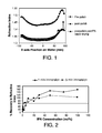
- FIG. 1 is a graph of the refractive index measured on various points along the diameter of the wafer before polishing, after polishing and after IPA vapor drying. It is evident from FIG. 1 that the dielectric properties can be restored with IPA vapor drying.
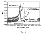
- Pieces of a PDEMS TM film having a dielectric constant of about 2.5 were measured for their initial refractive index. Some films were then immersed in a Coppeready TM CP72B cleaning solution (diluted 20:1 with Dl water) for 1 minute and some films were immersed for 5 minutes. The refractive index was measured after rinsing with DI water and after blow-drying with nitrogen. The films were then immersed in IPA-water solutions containing varying concentrations of IPA. Tables 3 and 4 tabulate the refractive index changes in the PDEMS TM films as a result of these processing steps.
- Table 3 IPA Conc.
- Figure 2 is a plot of the refractive index recovery using the above solutions having varied IPA concentrations after the immersion in Coppeready TM CP72B for 1 and 5 min exposure times. From the data plotted in Figure 2, it is evident that as much as 50% of the dielectric constant can be recovered using a restoration fluid having a concentration of only 5.0% IPA. 100% recovery of the dielectric constant can be obtained by employing a restoration fluid having a concentration of IPA of as little as 25%.
- a cleaning solution of Coppeready TM CP72B (Air Products and Chemicals, Inc., Allentown, PA) was diluted with DI water to a ratio of 20 parts by volume of water to one part by volume of Coppeready TM CP72B.
- Pieces of a wafer comprising a layer of PDEMS TM low dielectric constant material (Air Products and Chemicals, Inc., Allentown, PA) were immersed in the cleaning solution for 5 minutes. The pieces were then rinsed with DI water and then blow dried with nitrogen gas and the refractive index was measured. The pieces were then separately immersed for one minute in a restoration fluid comprising acetone, a restoration fluid comprising THF, and a restoration fluid comprising ethyl acetate to compare the restoration effect on the dielectric constant.
- Tables 5 and 6 illustrate that substantial restoration of the refractive index and the dielectric constant was achieved with the solvents tested.
- Table 5 PDEMS® 2.5 Dielectric Restoration Fluid 50/50 Acetone/water 50/50 THF/water 6/94 Ethyl acetate/water R.I. R.I. R.I.
- a cleaning solution of Coppeready TM CP72B (Air Products and Chemicals, Inc., Allentown, PA) was diluted with DI water to a ratio of 20 parts by volume of water to one part by volume of Coppeready TM CP72B.
- Pieces of a wafer comprising a layer of MesoElk TM porous organosilicate glass (Air Products and Chemicals, Inc., Allentown, PA) were immersed in the cleaning solution for 5 minutes. The pieces were then rinsed with DI water and then blow dried with nitrogen gas and the refractive index was measured. The pieces were then separately immersed for one minute in restoration fluids comprising various amounts of IPA. Table 7 illustrates that substantial restoration of the refractive index and, thus, the dielectric constant was achieved.
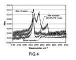
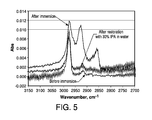
- Figures 3, 4 and 5 are IR spectra of the MesoElk® layers before and after treatment with each of the 10, 20 and 30% IPA restoration fluids, respectively. Significantly, a substantial reduction of the band at 2920 cm -1 and 2860 cm -1 is observed upon treatment.
Landscapes
- Internal Circuitry In Semiconductor Integrated Circuit Devices (AREA)
- Cleaning Or Drying Semiconductors (AREA)
- Detergent Compositions (AREA)
- Formation Of Insulating Films (AREA)
- Ceramic Capacitors (AREA)
- Organic Insulating Materials (AREA)
Applications Claiming Priority (1)
| Application Number | Priority Date | Filing Date | Title |
|---|---|---|---|
| US11/601,486 US7977121B2 (en) | 2006-11-17 | 2006-11-17 | Method and composition for restoring dielectric properties of porous dielectric materials |
Publications (2)
| Publication Number | Publication Date |
|---|---|
| EP1923905A2 true EP1923905A2 (de) | 2008-05-21 |
| EP1923905A3 EP1923905A3 (de) | 2009-06-24 |
Family
ID=38926343
Family Applications (1)
| Application Number | Title | Priority Date | Filing Date |
|---|---|---|---|
| EP07120803A Withdrawn EP1923905A3 (de) | 2006-11-17 | 2007-11-15 | Verfahren und Zusammensetzung zur Wiederherstellung von dielektrischen Eigenschaften von porösen Dielektrizitätsmaterialien |
Country Status (5)
| Country | Link |
|---|---|
| US (1) | US7977121B2 (de) |
| EP (1) | EP1923905A3 (de) |
| JP (1) | JP2008177540A (de) |
| KR (1) | KR20080045077A (de) |
| TW (1) | TW200824001A (de) |
Families Citing this family (7)
| Publication number | Priority date | Publication date | Assignee | Title |
|---|---|---|---|---|
| US7632771B2 (en) * | 2006-02-07 | 2009-12-15 | Imec | UV light exposure for functionalization and hydrophobization of pure-silica zeolites |
| US7977121B2 (en) * | 2006-11-17 | 2011-07-12 | Air Products And Chemicals, Inc. | Method and composition for restoring dielectric properties of porous dielectric materials |
| FR2910178B1 (fr) * | 2006-12-15 | 2009-05-15 | St Microelectronics Sa | Procede de realisation d'un element dielectrique poreux et element dielectrique correspondant |
| US8324093B2 (en) * | 2009-07-23 | 2012-12-04 | GlobalFoundries, Inc. | Methods for fabricating semiconductor devices including azeotropic drying processes |
| WO2011099768A2 (ko) * | 2010-02-09 | 2011-08-18 | 서강대학교산학협력단 | 고온 오존처리를 포함하는 나노기공 초저유전 박막의 제조 방법 및 이에 의해 제조된 나노기공 초저유전 박막 |
| TWI413185B (zh) * | 2010-08-19 | 2013-10-21 | 國立交通大學 | 一種形成鍺半導體表面保護層的方法 |
| EP2884523B1 (de) * | 2013-12-16 | 2020-02-05 | IMEC vzw | Verfahren zum Aktivieren einer porösen Schichtoberfläche |
Family Cites Families (33)
| Publication number | Priority date | Publication date | Assignee | Title |
|---|---|---|---|---|
| US5470802A (en) | 1994-05-20 | 1995-11-28 | Texas Instruments Incorporated | Method of making a semiconductor device using a low dielectric constant material |
| US5504042A (en) | 1994-06-23 | 1996-04-02 | Texas Instruments Incorporated | Porous dielectric material with improved pore surface properties for electronics applications |
| EP0775669B1 (de) | 1995-11-16 | 2001-05-02 | Texas Instruments Incorporated | Wenig flüchtiges Lösungsmittel enthaltender Vorläufer für nanoporöses Aerogel |
| JPH1070121A (ja) | 1995-11-16 | 1998-03-10 | Texas Instr Inc <Ti> | 半導体基板上に薄膜ナノ多孔質アエロゲルを形成するための低揮発性溶剤基の方法 |
| US6037277A (en) * | 1995-11-16 | 2000-03-14 | Texas Instruments Incorporated | Limited-volume apparatus and method for forming thin film aerogels on semiconductor substrates |
| US6503850B1 (en) | 1997-04-17 | 2003-01-07 | Alliedsignal Inc. | Process for producing nanoporous dielectric films at high pH |
| US6022812A (en) | 1998-07-07 | 2000-02-08 | Alliedsignal Inc. | Vapor deposition routes to nanoporous silica |
| US6372666B1 (en) | 1998-08-31 | 2002-04-16 | Alliedsignal Inc. | Process for producing dielectric thin films |
| US6312793B1 (en) | 1999-05-26 | 2001-11-06 | International Business Machines Corporation | Multiphase low dielectric constant material |
| CN1460037A (zh) | 2000-03-13 | 2003-12-03 | 马特森技术公司 | 处理电子元件的方法及装置 |
| CA2413592A1 (en) | 2000-06-23 | 2002-01-03 | Nigel P. Hacker | Method to restore hydrophobicity in dielectric films and materials |
| US6573131B2 (en) | 2000-07-13 | 2003-06-03 | The Regents Of The University Of California | Silica zeolite low-k dielectric thin films and methods for their production |
| US6632748B2 (en) * | 2001-03-27 | 2003-10-14 | Samsung Electronics Co., Ltd. | Composition for preparing substances having nano-pores |
| TW200303581A (en) | 2002-02-28 | 2003-09-01 | Tech Ltd A | Method and apparatus for cleaning and drying semiconductor wafer |
| US6843855B2 (en) | 2002-03-12 | 2005-01-18 | Applied Materials, Inc. | Methods for drying wafer |
| JP4349606B2 (ja) | 2002-03-25 | 2009-10-21 | 大日本スクリーン製造株式会社 | 基板洗浄方法 |
| KR100649418B1 (ko) * | 2002-08-22 | 2006-11-27 | 다이킨 고교 가부시키가이샤 | 박리액 |
| US6972083B2 (en) * | 2002-09-27 | 2005-12-06 | Agere Systems, Inc. | Electrochemical method and system for monitoring hydrogen peroxide concentration in slurries |
| JP2004140196A (ja) | 2002-10-17 | 2004-05-13 | Nec Electronics Corp | 半導体装置の製造方法および基板洗浄装置 |
| US7485611B2 (en) * | 2002-10-31 | 2009-02-03 | Advanced Technology Materials, Inc. | Supercritical fluid-based cleaning compositions and methods |
| US20040175942A1 (en) * | 2003-01-03 | 2004-09-09 | Chang Song Y. | Composition and method used for chemical mechanical planarization of metals |
| US20040198066A1 (en) | 2003-03-21 | 2004-10-07 | Applied Materials, Inc. | Using supercritical fluids and/or dense fluids in semiconductor applications |
| US7074727B2 (en) | 2003-07-09 | 2006-07-11 | Taiwan Semiconductor Manufacturing Company, Ltd. | Process for improving dielectric properties in low-k organosilicate dielectric material |
| US20050076580A1 (en) * | 2003-10-10 | 2005-04-14 | Air Products And Chemicals, Inc. | Polishing composition and use thereof |
| US20050205835A1 (en) * | 2004-03-19 | 2005-09-22 | Tamboli Dnyanesh C | Alkaline post-chemical mechanical planarization cleaning compositions |
| US20060081273A1 (en) * | 2004-10-20 | 2006-04-20 | Mcdermott Wayne T | Dense fluid compositions and processes using same for article treatment and residue removal |
| KR101238471B1 (ko) * | 2005-02-25 | 2013-03-04 | 이케이씨 테크놀로지, 인코포레이티드 | 구리 및 저 k 유전체 물질을 갖는 기판으로부터 레지스트,에칭 잔류물 및 구리 산화물을 제거하는 방법 |
| US7385231B2 (en) * | 2005-08-31 | 2008-06-10 | Fujifilmcorporation | Porous thin-film-deposition substrate, electron emitting element, methods of producing them, and switching element and display element |
| US7468330B2 (en) * | 2006-04-05 | 2008-12-23 | International Business Machines Corporation | Imprint process using polyhedral oligomeric silsesquioxane based imprint materials |
| US7977121B2 (en) * | 2006-11-17 | 2011-07-12 | Air Products And Chemicals, Inc. | Method and composition for restoring dielectric properties of porous dielectric materials |
| US7500397B2 (en) * | 2007-02-15 | 2009-03-10 | Air Products And Chemicals, Inc. | Activated chemical process for enhancing material properties of dielectric films |
| US20090291873A1 (en) * | 2008-05-22 | 2009-11-26 | Air Products And Chemicals, Inc. | Method and Composition for Post-CMP Cleaning of Copper Interconnects Comprising Noble Metal Barrier Layers |
| US8283260B2 (en) * | 2008-08-18 | 2012-10-09 | Air Products And Chemicals, Inc. | Process for restoring dielectric properties |
-
2006
- 2006-11-17 US US11/601,486 patent/US7977121B2/en not_active Expired - Fee Related
-
2007
- 2007-11-12 TW TW096142704A patent/TW200824001A/zh unknown
- 2007-11-15 EP EP07120803A patent/EP1923905A3/de not_active Withdrawn
- 2007-11-16 KR KR1020070117502A patent/KR20080045077A/ko not_active Ceased
- 2007-11-16 JP JP2007298091A patent/JP2008177540A/ja active Pending
Also Published As
| Publication number | Publication date |
|---|---|
| KR20080045077A (ko) | 2008-05-22 |
| TW200824001A (en) | 2008-06-01 |
| JP2008177540A (ja) | 2008-07-31 |
| US20080118995A1 (en) | 2008-05-22 |
| EP1923905A3 (de) | 2009-06-24 |
| US7977121B2 (en) | 2011-07-12 |
Similar Documents
| Publication | Publication Date | Title |
|---|---|---|
| JP5775116B2 (ja) | 有機シリケート材料からの炭素の除去方法 | |
| US11447642B2 (en) | Methods of using surface treatment compositions | |
| US7500397B2 (en) | Activated chemical process for enhancing material properties of dielectric films | |
| TWI582230B (zh) | A cleaning solution for a semiconductor element, and a cleaning method using the cleaning solution | |
| KR100887225B1 (ko) | 반도체 디바이스의 제조 방법 | |
| US8206788B2 (en) | Method for treating a damaged porous dielectric | |
| EP1923905A2 (de) | Verfahren und Zusammensetzung zur Wiederherstellung von dielektrischen Eigenschaften von porösen Dielektrizitätsmaterialien | |
| EP2128707B1 (de) | Reinigungszusammensetzung und prozess zum herstellen einer halbleiteranordnung | |
| EP3973565A1 (de) | Zusammensetzung und verfahren zum selektiven ätzen einer hartmaske und/oder einer ätzstoppschicht in gegenwart von schichten aus low-k-materialien, kupfer, kobalt und/oder wolfram | |
| KR100383498B1 (ko) | 반도체 장치 제조방법 | |
| EP1195801B1 (de) | Verfahren zur Behandlung einer Isolierschicht mit niedriger Dielektrizitätskonstante | |
| JP2002110497A (ja) | 半導体装置の製造方法、ウェハ処理装置、及びウェハ保管箱 | |
| Saga et al. | Wafer cleaning using supercritical CO2 in semiconductor and nanoelectronic device fabrication | |
| Xie et al. | The restoration of porous methylsilsesquioxane (p-MSQ) films using trimethylhalosilanes dissolved in supercritical carbon dioxide | |
| Tsui et al. | A novel wafer reclaim method for amorphous SiC and carbon doped oxide films | |
| TW201938783A (zh) | 用以去除乾蝕刻殘渣之洗淨液及使用此洗淨液之半導體基板之製造方法 | |
| US20040188675A1 (en) | Semiconductor device and method of manufacturing the same | |
| Huang et al. | Intra-level voltage ramping-up to dielectric breakdown failure on Cu/porous low-k interconnections in 45 nm ULSI generation | |
| Louis et al. | Wet or plasma clean? Competing or complementary? A dual damascene study with Si-OC-H dielectric on copper wiring | |
| TW202346541A (zh) | 用於多晶矽挖掘的配製鹼性化學物質 | |
| Aiello | Investigation of a Self-Assembled Monolayer as a Cu Diffusion Barrier for Solar Cell Metallization | |
| JP2007208010A (ja) | 半導体装置の製造方法 | |
| KR20100032652A (ko) | 초임계이산화탄소 내에서 손상된 낮은 유전 상수의 오가노실리케이트 필름의 소수성을 복원하는 방법 |
Legal Events
| Date | Code | Title | Description |
|---|---|---|---|
| PUAI | Public reference made under article 153(3) epc to a published international application that has entered the european phase |
Free format text: ORIGINAL CODE: 0009012 |
|
| AK | Designated contracting states |
Kind code of ref document: A2 Designated state(s): AT BE BG CH CY CZ DE DK EE ES FI FR GB GR HU IE IS IT LI LT LU LV MC MT NL PL PT RO SE SI SK TR |
|
| AX | Request for extension of the european patent |
Extension state: AL BA HR MK RS |
|
| PUAL | Search report despatched |
Free format text: ORIGINAL CODE: 0009013 |
|
| AK | Designated contracting states |
Kind code of ref document: A3 Designated state(s): AT BE BG CH CY CZ DE DK EE ES FI FR GB GR HU IE IS IT LI LT LU LV MC MT NL PL PT RO SE SI SK TR |
|
| AX | Request for extension of the european patent |
Extension state: AL BA HR MK RS |
|
| 17P | Request for examination filed |
Effective date: 20090730 |
|
| 17Q | First examination report despatched |
Effective date: 20090828 |
|
| AKX | Designation fees paid |
Designated state(s): AT BE BG CH CY CZ DE DK EE ES FI FR GB GR HU IE IS IT LI LT LU LV MC MT NL PL PT RO SE SI SK TR |
|
| STAA | Information on the status of an ep patent application or granted ep patent |
Free format text: STATUS: THE APPLICATION IS DEEMED TO BE WITHDRAWN |
|
| 18D | Application deemed to be withdrawn |
Effective date: 20130601 |