EP1923902A1 - Source de pulvérisation magnétron, système de revêtement par pulvérisation et procédé pour revêtir un substrat - Google Patents
Source de pulvérisation magnétron, système de revêtement par pulvérisation et procédé pour revêtir un substrat Download PDFInfo
- Publication number
- EP1923902A1 EP1923902A1 EP06124060A EP06124060A EP1923902A1 EP 1923902 A1 EP1923902 A1 EP 1923902A1 EP 06124060 A EP06124060 A EP 06124060A EP 06124060 A EP06124060 A EP 06124060A EP 1923902 A1 EP1923902 A1 EP 1923902A1
- Authority
- EP
- European Patent Office
- Prior art keywords
- target
- coating
- plasma
- sputtering source
- magnetron sputtering
- Prior art date
- Legal status (The legal status is an assumption and is not a legal conclusion. Google has not performed a legal analysis and makes no representation as to the accuracy of the status listed.)
- Granted
Links
- 238000000576 coating method Methods 0.000 title claims abstract description 126
- 239000011248 coating agent Substances 0.000 title claims abstract description 118
- 238000004544 sputter deposition Methods 0.000 title claims abstract description 63
- 238000001755 magnetron sputter deposition Methods 0.000 title claims abstract description 46
- 239000000758 substrate Substances 0.000 title claims abstract description 41
- 238000000034 method Methods 0.000 title claims abstract description 24
- 239000000463 material Substances 0.000 claims abstract description 13
- 230000000694 effects Effects 0.000 claims description 18
- 238000009434 installation Methods 0.000 claims description 15
- 230000036961 partial effect Effects 0.000 claims description 10
- 230000002829 reductive effect Effects 0.000 claims description 5
- 230000009471 action Effects 0.000 claims description 4
- 230000009467 reduction Effects 0.000 abstract description 2
- 238000004519 manufacturing process Methods 0.000 abstract 2
- 210000002381 plasma Anatomy 0.000 description 106
- 230000003628 erosive effect Effects 0.000 description 11
- 239000013077 target material Substances 0.000 description 11
- 238000009826 distribution Methods 0.000 description 7
- 238000001816 cooling Methods 0.000 description 6
- 230000008569 process Effects 0.000 description 6
- XKRFYHLGVUSROY-UHFFFAOYSA-N Argon Chemical compound [Ar] XKRFYHLGVUSROY-UHFFFAOYSA-N 0.000 description 4
- IJGRMHOSHXDMSA-UHFFFAOYSA-N Atomic nitrogen Chemical compound N#N IJGRMHOSHXDMSA-UHFFFAOYSA-N 0.000 description 4
- 238000006243 chemical reaction Methods 0.000 description 4
- 150000001875 compounds Chemical class 0.000 description 4
- 238000002844 melting Methods 0.000 description 4
- 230000008018 melting Effects 0.000 description 4
- 230000008901 benefit Effects 0.000 description 3
- 238000010891 electric arc Methods 0.000 description 3
- 239000011261 inert gas Substances 0.000 description 3
- 150000002500 ions Chemical class 0.000 description 3
- 238000010943 off-gassing Methods 0.000 description 3
- 229910017840 NH 3 Inorganic materials 0.000 description 2
- 229910052786 argon Inorganic materials 0.000 description 2
- QVGXLLKOCUKJST-UHFFFAOYSA-N atomic oxygen Chemical compound [O] QVGXLLKOCUKJST-UHFFFAOYSA-N 0.000 description 2
- 230000015572 biosynthetic process Effects 0.000 description 2
- 238000010586 diagram Methods 0.000 description 2
- 238000005516 engineering process Methods 0.000 description 2
- 239000007789 gas Substances 0.000 description 2
- 238000010438 heat treatment Methods 0.000 description 2
- 229910052757 nitrogen Inorganic materials 0.000 description 2
- 230000010355 oscillation Effects 0.000 description 2
- 239000001301 oxygen Substances 0.000 description 2
- 229910052760 oxygen Inorganic materials 0.000 description 2
- -1 ITO Chemical class 0.000 description 1
- 229910004298 SiO 2 Inorganic materials 0.000 description 1
- 230000008859 change Effects 0.000 description 1
- 210000000078 claw Anatomy 0.000 description 1
- 230000001419 dependent effect Effects 0.000 description 1
- 238000007667 floating Methods 0.000 description 1
- 230000002452 interceptive effect Effects 0.000 description 1
- 230000000670 limiting effect Effects 0.000 description 1
- 230000007774 longterm Effects 0.000 description 1
- 239000000155 melt Substances 0.000 description 1
- 229910052751 metal Inorganic materials 0.000 description 1
- 239000002184 metal Substances 0.000 description 1
- 229910001092 metal group alloy Inorganic materials 0.000 description 1
- 150000002739 metals Chemical class 0.000 description 1
- 229910052755 nonmetal Inorganic materials 0.000 description 1
- 238000011084 recovery Methods 0.000 description 1
- 230000002441 reversible effect Effects 0.000 description 1
- 238000004904 shortening Methods 0.000 description 1
- 238000005507 spraying Methods 0.000 description 1
- 239000000126 substance Substances 0.000 description 1
- 230000001360 synchronised effect Effects 0.000 description 1
- 230000002277 temperature effect Effects 0.000 description 1
- 239000010409 thin film Substances 0.000 description 1
Images


Classifications
-
- H—ELECTRICITY
- H01—ELECTRIC ELEMENTS
- H01J—ELECTRIC DISCHARGE TUBES OR DISCHARGE LAMPS
- H01J37/00—Discharge tubes with provision for introducing objects or material to be exposed to the discharge, e.g. for the purpose of examination or processing thereof
- H01J37/32—Gas-filled discharge tubes
- H01J37/34—Gas-filled discharge tubes operating with cathodic sputtering
- H01J37/3402—Gas-filled discharge tubes operating with cathodic sputtering using supplementary magnetic fields
- H01J37/3405—Magnetron sputtering
- H01J37/3408—Planar magnetron sputtering
-
- C—CHEMISTRY; METALLURGY
- C23—COATING METALLIC MATERIAL; COATING MATERIAL WITH METALLIC MATERIAL; CHEMICAL SURFACE TREATMENT; DIFFUSION TREATMENT OF METALLIC MATERIAL; COATING BY VACUUM EVAPORATION, BY SPUTTERING, BY ION IMPLANTATION OR BY CHEMICAL VAPOUR DEPOSITION, IN GENERAL; INHIBITING CORROSION OF METALLIC MATERIAL OR INCRUSTATION IN GENERAL
- C23C—COATING METALLIC MATERIAL; COATING MATERIAL WITH METALLIC MATERIAL; SURFACE TREATMENT OF METALLIC MATERIAL BY DIFFUSION INTO THE SURFACE, BY CHEMICAL CONVERSION OR SUBSTITUTION; COATING BY VACUUM EVAPORATION, BY SPUTTERING, BY ION IMPLANTATION OR BY CHEMICAL VAPOUR DEPOSITION, IN GENERAL
- C23C14/00—Coating by vacuum evaporation, by sputtering or by ion implantation of the coating forming material
- C23C14/22—Coating by vacuum evaporation, by sputtering or by ion implantation of the coating forming material characterised by the process of coating
- C23C14/34—Sputtering
- C23C14/3407—Cathode assembly for sputtering apparatus, e.g. Target
-
- C—CHEMISTRY; METALLURGY
- C23—COATING METALLIC MATERIAL; COATING MATERIAL WITH METALLIC MATERIAL; CHEMICAL SURFACE TREATMENT; DIFFUSION TREATMENT OF METALLIC MATERIAL; COATING BY VACUUM EVAPORATION, BY SPUTTERING, BY ION IMPLANTATION OR BY CHEMICAL VAPOUR DEPOSITION, IN GENERAL; INHIBITING CORROSION OF METALLIC MATERIAL OR INCRUSTATION IN GENERAL
- C23C—COATING METALLIC MATERIAL; COATING MATERIAL WITH METALLIC MATERIAL; SURFACE TREATMENT OF METALLIC MATERIAL BY DIFFUSION INTO THE SURFACE, BY CHEMICAL CONVERSION OR SUBSTITUTION; COATING BY VACUUM EVAPORATION, BY SPUTTERING, BY ION IMPLANTATION OR BY CHEMICAL VAPOUR DEPOSITION, IN GENERAL
- C23C14/00—Coating by vacuum evaporation, by sputtering or by ion implantation of the coating forming material
- C23C14/22—Coating by vacuum evaporation, by sputtering or by ion implantation of the coating forming material characterised by the process of coating
- C23C14/34—Sputtering
- C23C14/3485—Sputtering using pulsed power to the target
-
- C—CHEMISTRY; METALLURGY
- C23—COATING METALLIC MATERIAL; COATING MATERIAL WITH METALLIC MATERIAL; CHEMICAL SURFACE TREATMENT; DIFFUSION TREATMENT OF METALLIC MATERIAL; COATING BY VACUUM EVAPORATION, BY SPUTTERING, BY ION IMPLANTATION OR BY CHEMICAL VAPOUR DEPOSITION, IN GENERAL; INHIBITING CORROSION OF METALLIC MATERIAL OR INCRUSTATION IN GENERAL
- C23C—COATING METALLIC MATERIAL; COATING MATERIAL WITH METALLIC MATERIAL; SURFACE TREATMENT OF METALLIC MATERIAL BY DIFFUSION INTO THE SURFACE, BY CHEMICAL CONVERSION OR SUBSTITUTION; COATING BY VACUUM EVAPORATION, BY SPUTTERING, BY ION IMPLANTATION OR BY CHEMICAL VAPOUR DEPOSITION, IN GENERAL
- C23C14/00—Coating by vacuum evaporation, by sputtering or by ion implantation of the coating forming material
- C23C14/22—Coating by vacuum evaporation, by sputtering or by ion implantation of the coating forming material characterised by the process of coating
- C23C14/34—Sputtering
- C23C14/35—Sputtering by application of a magnetic field, e.g. magnetron sputtering
-
- H—ELECTRICITY
- H01—ELECTRIC ELEMENTS
- H01J—ELECTRIC DISCHARGE TUBES OR DISCHARGE LAMPS
- H01J37/00—Discharge tubes with provision for introducing objects or material to be exposed to the discharge, e.g. for the purpose of examination or processing thereof
- H01J37/32—Gas-filled discharge tubes
- H01J37/34—Gas-filled discharge tubes operating with cathodic sputtering
- H01J37/3411—Constructional aspects of the reactor
- H01J37/3414—Targets
- H01J37/3423—Shape
-
- H—ELECTRICITY
- H01—ELECTRIC ELEMENTS
- H01J—ELECTRIC DISCHARGE TUBES OR DISCHARGE LAMPS
- H01J37/00—Discharge tubes with provision for introducing objects or material to be exposed to the discharge, e.g. for the purpose of examination or processing thereof
- H01J37/32—Gas-filled discharge tubes
- H01J37/34—Gas-filled discharge tubes operating with cathodic sputtering
- H01J37/3411—Constructional aspects of the reactor
- H01J37/345—Magnet arrangements in particular for cathodic sputtering apparatus
- H01J37/3455—Movable magnets
Definitions
- Sputtering or (cathode) sputtering is a commonly used technology for producing thin films on substrates.
- a target is bombarded with ions, such as inert gas ions from an ignited plasma.
- ions such as inert gas ions from an ignited plasma.
- the material which is intended directly or indirectly for coating is sputtered from the target, that is to say released or atomized.
- the sputtered material is deposited, possibly after a chemical reaction, on the substrate opposite the target.
- the substrate may be either stationary relative to the target during the coating process, or continuously transported past the target.
- a magnetron sputter source has a magnet arrangement, which is arranged on the side of the target facing away from the substrate.
- the magnet system generates a magnetic field and influences the coating plasma, which forms on the substrate side in an area above the target surface.
- an inhomogeneous plasma structure forms over the surface of the target, which leads to a non-uniform erosion of the target material.
- Magnetic arrangements are typically used which generate plasma channels in closed form, for example in the form of an elongated oval (race track).
- the inhomogeneity of the plasma leads to the formation of erosion ditches in the target.
- the target material can not be completely used up, on the other hand lead the Inhomogeneous erosion and the formation of erosion ditches to a non-homogeneous and uniform coating of the substrate.
- a cooling device can only reduce the temperature of the uppermost atomic layers of the target limited.
- the maximum possible power density is limited by the occurrence of arcing at power densities higher than about 3 W / cm 2 .
- the magnetron sputtering source according to the invention for a coating installation comprises at least one cathode and at least one cathode-assigned or cathode-forming target which provides coating and / or treatment material for coating and / or treatment, means for generating a coating plasma and at least one magnet arrangement Generation of a magnetic field for influencing the coating plasma such that at least over a partial area of the target at least one plasma channel is generated.
- the magnet arrangement and the surface of the target are arranged to be movable relative to each other so that the plasma channel can be moved over the surface of the target.
- the magnetron sputtering source is set such that, in order to reduce the heat load on the target surface, the exposure time of the plasma to the surface region is reduced by increasing the relative velocity between the magnet assembly and the target.
- the exposure time is calculated as the quotient of the width of the plasma channel (the width in this context is the extension of the plasma channel along the direction of movement), which covers the surface area, and the scan speed.
- the sputtering rate can be adapted to the exposure time, in particular so far increased that (despite high sputtering rate) no undesired surface effects occur.
- the area ratio between the total target area and the plasma channel must be so high that sufficient cooling of the surface takes place prior to the next scanning of said surface area.
- the exposure time of the plasma refers to a single movement of the plasma channel over the surface area of the target. The larger the area ratio between the entire target surface and the surface of the plasma channel or plasma channels, the greater are the "recovery times" for the surface areas of the target at a given velocity profile along the path of the plasma channel (and with a complete scanning of the surface) two consecutive scans / plasma effects.
- a magnetron sputtering source for a coating system comprising at least one cathode and at least one cathode associated target, which provides coating and / or treatment material for coating and / or treatment, means for generating a coating plasma and at least one magnet arrangement for Generation of a magnetic field for influencing the coating plasma such that at least over a partial area of the target at least one plasma channel is generated.
- the magnet arrangement and the surface of the target are arranged to be movable relative to one another by means of a drive.
- the drive is set such that during a coating cycle a speed of the relative movement of at least 0.1 m / s is exceeded.
- a magnetron sputtering source for a coating system comprising at least one cathode and at least one cathode associated target, which provides coating and / or treatment material for coating and / or treatment, means for generating a coating plasma and at least one magnet arrangement for generating a magnetic field for influencing the coating plasma in such a way that at least one plasma channel is generated at least over a partial area of the target.
- the magnet assembly and the surface of the target are arranged to be movable relative to one another.
- the magnetron sputtering source is adjusted so that the power density at least temporarily reaches a value of at least 5 W / cm 2 , wherein the relative speed between the magnet assembly and the target depending on the power density (and thus the sputtering rate) is set so high that no undesirable temperature-induced surface effects on the target surface occur.
- the present invention is based on the recognition that the thermal inertia of the surface of the target can be exploited in order to work with higher power densities and consequently higher sputtering rates.
- the power density corresponds to the power introduced into the system per cathode surface unit.
- the power density is functionally related to the sputtering rate.
- the plasma is significantly shortened to a surface area of the target as the plasma channel moves relative to the surface area. Due to the shorter time period of the action of the plasma during an "overscan" of the surface area, power densities or sputtering rates can be shifted upward without significant undesirable surface effects on the target surface, such as, for example, As arcing, melting of the target, local outgassing of the target, chemical reactions of compounds in the target, etc., occur. As a result, overall, the energy input into a surface area (with a certain unit area) can be increased over a given (short) period of time without surface effects on the target surface.
- the target can be "scanned" several times from the plasma channel, whereby the temperature of the uppermost atomic layers of the target increases significantly less than in the case of one longer, albeit less powerful action of the plasma.
- a surface area is scanned several times during a coating cycle, it is preferably ensured that the time between the two exposure phases is sufficiently large for a cooling of the surface.
- the heating during scanning depends on the total energy supplied and on the sequence in which the energy is supplied. It has been recognized that more meaningful sequences of energy input are possible than a virtually constant supply of total energy with a low sputtering rate.
- the velocity profile is adjusted to the duration of the plasma over the target.
- the relative movement between the magnet arrangement and the surface of the target should be interpreted widely within the scope of the invention.
- the target or the cathode can move relative to the magnet arrangement.
- the magnet assembly may be movable relative to the target or to the cathode.
- both components, magnet assembly and cathode or target are arranged relative to each other and movable relative to the coating system.
- the magnet system is arranged on the side facing away from the substrate to be coated of the target to be atomized.
- the magnet arrangement in particular comprises one or more magnets, in particular permanent magnets, and at least one yoke.
- the magnet system can generate one or more plasma channels which are arranged side by side or in one another.
- plasma channels are race tracks (a substantially elongated, oval, closed track), a bone-shaped, closed path or a closed path similar to a rhombus in question.
- the invention is suitable for all common sputtering processes, for example for sputtering with inert gas (argon, etc.), sputtering with reactive gas (oxygen, nitrogen, NH 3 , etc.)
- reactive gas oxygen, nitrogen, NH 3 , etc.
- target materials can be used. These may be, for example, metals, metal alloys, or metal-nonmetal compounds such as ITO, IZO, ZnO: Al, SiO 2 , IGZO (InGaZnO).
- the thickness of the target can be increased at the two reversal points or reversal portions of the movement of the magnet system relative to the thickness of the material over the remaining target surface, since in the reversal regions due to the velocity profile naturally greater erosion occurs.
- This measure makes it possible to obtain a minimum and uniform Tartrestdicke over the entire target at the end of the target life, with the advantage of a correspondingly high target utilization.
- the perpendicular distance of the magnet system from the target rear side in the reversal regions can be increased and / or the power supply in the reversal regions can be reduced in order to prevent faster erosion in these regions compared to the remaining surface regions.
- better coating results are achieved when the reversal region lies in the edge region of the target, since higher Yields in this range are desirable for uniform coating.
- a surface area of the target in the sense of the claims is a small surface area of the surface of the target, in particular the partial area of the target covered by the plasma channel, compared to the entire area which the plasma channel acts on during the scanning.
- the surface area can be an infinitesimally small area, via which the influence or the effect of the plasma moving over the area is determined in any case.
- the advantages of the magnetron sputtering source according to the invention lie primarily in the possibility of using higher sputtering rates. Due to the higher sputtering rates, a coating system can be shortened with a constant cycle time, which leads to a reduction of the acquisition and operating costs. In addition, it has been shown that large-area coatings which are to be deposited statically (such as TFT coatings) can be realized with the inventive concept with much more homogeneous layer thickness distributions than with conventional technologies which use a plurality of cathodes arranged in parallel.
- the drive is set such that during a coating cycle a speed of the relative movement of at least 0.1 m / s, in particular 0.2 m / s, in particular 0.3 m / s, in particular 0 , 5 m / s, in particular of 1.0 m / s, in particular of 3.0 m / s, in particular of 5.0 m / s, is exceeded.
- suitable drives e.g. Belt drives or linear motors, the mentioned high speeds can be easily realized.
- Each surface area of the target surface is under the influence of the coating plasma during overscanning for a certain period of time, the time being inversely proportional to the relative velocity of movement between the plasma channel and the target surface. This means that by increasing the speed, a shortening of the exposure time of the plasma is achieved on the surface area. This in turn makes it possible to use higher sputtering rates during scanning.
- the magnet system can oscillate, for example, between the two parallel, in particular between the two shorter target edges. This oscillation can be superimposed by movements in the remaining spatial directions (that is, not parallel to the central longitudinal axis of the target).
- the instantaneous velocity may be constant over most of the trajectory relative to the target surface. This constant speed should at least reach the minimum speed values mentioned in the claims. Alternatively, the instantaneous speed can also be variable to z.
- B. adapt layer thickness distributions or target erosion profiles. It is clear that in the presence of inflection points and decelerations of the relative motion, the speed temporarily drops to lower values or to zero.
- the scanning speed should exceed the speed values mentioned in the claims over a larger part of the path over the target surface, preferably over 50% of the web length, particularly preferably over 75% of the web length, during a coating cycle.
- the high speed scanned area is even larger.
- the magnetron sputtering source is set such that the power density at least temporarily has a value of at least 5 W / cm 2 , in particular a value of at least 15 W / cm 2 , in particular a value of 30 W / cm 2 , in particular a value of 50 W / cm 2 , in particular a value of 75 W / cm 2 , achieved.
- the loading of the surface of the target by an increase in the sputtering rate is compensated by an increase in the scan (scanning) speed and thus the exposure time of the plasma to the surface area.
- the magnetron sputtering source according to the invention is designed or set for operation with such power densities.
- the adjustment of the relative velocity between the magnet assembly and the surface of the target is based on the ratio of the size of the total surface of the target to the surface of the plasma channel projected onto the target surface and the surface on the surface of the target to which the plasma has a significant effect , and depending on the desired sputtering rate.
- the maximum speed is set, so that an associated maximum sputtering rate, which is determined empirically, can be realized.
- the ratio of the total surface area of the target to the surface of the plasma channel is at least 15, in particular 30, in particular 45, in particular 90.
- Said area ratio is in conjunction with the other variables that can be matched, namely the velocity profile and the profile of the sputtering rate (over the path). , also important. This ratio determines the intervals at which a certain surface area of the target surface is under the influence of the plasma.
- the ratio of the total sputtering surface of the target to the surface of the plasma channel or the plasma channels must be chosen sufficiently large that each surface area can cool sufficiently before the next scan. Since the largest possible area ratio ensures good cooling, the process is particularly suitable for large-area coatings with large-area targets.
- a sufficiently high speed combined with high sputtering rates can be realized.
- the area ratio indirectly determines the maximum possible sputtering rate via the adjustable speed.
- the sputtering source is preferably set such that the total exposure time of the plasma to a specific surface area of the target per coating cycle is subdivided into at least two temporally separate periods of time.
- the coating cycle is considered to be a cycle for coating a substrate with the intended coating carried out in the station.
- a coating cycle however, a time-closed coating process can be considered in which several substrates are coated directly one behind the other.
- each surface area of the target is short-flashed by the high scanning speed and two or more times during a coating cycle under the influence of the plasma.
- the thermal inertia of the target material is utilized, which does not overheat during the short scan duration and sufficiently cools down through a suitable area ratio (as described above) between two scan cycles.
- the target is preferably rectangular with a length and a width wherein preferably the length is a multiple of the width, and the magnet arrangement and the target are arranged to be movable relative to one another at least along the direction of the length of the target.
- This movement can be superimposed by movements in other spatial directions.
- an oscillating relative movement can be performed between the two transverse edges.
- the target may be formed with a substantially flat and / or curved surface.
- the target may be mounted on a cooled backplate, such as by bonding, claws, screws, spraying, etc.
- the target may be formed either as a planar cathode or as a domed cathode, for example 2.5m x 0.3m in size.
- the target may also be formed as a surface cathode or as a curved surface cathode, for example, with a size of 2, 5 m x 2 m.
- the magnetron sputtering source may also be a rotatable magnetron tube sputtering source having a tube cathode and / or a rotatable tube target.
- the relative speed between target and magnet system corresponds here to the path velocity of the target surface relative to the magnet system.
- the area ratio between the total surface area of the target and the area of the plasma channel can be achieved inter alia by increasing the target diameter.
- the principle of the invention should refer to all possible rotatable cathodes / targets where the description specifies planar targets.
- At least one anode or anode arrangement is provided for receiving electrons to be dissipated.
- the anode may be formed by the surroundings of the magnetron cathode, for example the chamber wall, a dark space frame, a circumferential profile, etc.
- the anode or anode arrangement may in particular also comprise at least one electrode which, relative to the target, over the Target surface is arranged movable.
- the electrode will usually move in synchronism with the magnet system relative to the target.
- the electrode may be arranged along a plasma channel.
- the anode or anode assembly may include a plurality of electrodes disposed immovable or fixed relative to the target over the target surface.
- one or more cooled or uncooled bars can be used as anodes, which are located along the direction of movement of the magnet system in front of the target or the target edge and / or parallel to the magnet system in front of the target.
- the electrodes act punctually in the plasma channel and are electrically connected in synchronism with the movement of the magnet system.
- the target may preferably consist of one or more segments which are galvanically coupled or separated. If the target is subdivided into mutually decoupled segments, means may be provided which switch at least one segment as a cathode, while at least one adjacent segment is connected as an anode.
- the electrical potential of the individual target segments can be synchronized with the movement of the magnet system, i. the target segments can be electrically switched in synchronism with the movement of the magnet system. For example, the negative sputtering potential is only applied to that target segment which is traversed by the magnet system at the given time. The remaining target segments are not at sputtering potential but, for example, at ground, at positive or floating potential.
- the means for generating a coating plasma may include a power supply device comprising an AC, a DC, a unipolar pulsed, a bipolar pulsed, or an RF (radio frequency) source. From this source, the power is coupled into the system.
- a power supply device comprising an AC, a DC, a unipolar pulsed, a bipolar pulsed, or an RF (radio frequency) source. From this source, the power is coupled into the system.
- the object according to the invention is also achieved by a sputter-coating installation comprising at least one treatment or coating space, and a magnetron sputtering source as described above.
- the exposure time of the plasma to the surface region is reduced by increasing the relative velocity between the magnet assembly and the target.
- the relative velocity between the magnetic field and the target exceeds a value of at least 0.1 m / s.
- the plasma channel is conducted at high speed (relatively) over a surface area of the target, so that a period of time in which the plasma continuously acts on the surface area is shortened such that even at high power density (and therefore high sputtering rate) no significant undesirable Surface effects occur at the target surface.
- the relative velocity of the plasma channel with respect to the surface of the target exceeds a value of 0.1 m / s, in particular of 0.2 m / s, in particular of 0.3 m / s, in particular of 0.5 m / s, in particular of 1.0 m / s, in particular 3.0 m / s, in particular of 5.0 m / s.
- the plasma channel has an oval, a long oval, a bony or a rhomboid shape.
- the power density at least temporarily preferably reaches a value of at least 5 W / cm 2 , in particular a value of at least 15 W / cm 2 , in particular a value of 30 W / cm 2 , in particular one Value of 50 W / cm 2 , in particular a value of 75 W / cm 2 .
- the magnetron sputtering source according to the invention is designed or set for operation with such power densities.
- the magnetic field influences the plasma to form at least one plasma channel, in particular in an oval shape (race track), a bone-like shape and / or in the form of a rhombus.
- a ratio of the total sputtering surface of the target to the surface of the target projected plasma channel surface exceeds a value of 15, in particular of 30, in particular 45, in particular of 90. Is the plasma channel generated in step c) relative to Area of the target small area, the time intervals between which a surface area of the target surface is scanned, relatively large.
- the target is rectangular in length and width, the length being a multiple of the width, and the magnetic field moving at least along the direction of the length of the target relative to the target.
- the magnetic field may oscillate relative to the edges of the target.
- the total exposure time of the plasma to a specific surface area of the target surface can be subdivided per coating cycle into at least two temporally separate periods of time.
- FIG. 1 A sectional view of a coating system according to the invention
- FIG. 2 A side sectional view of a coating system according to the invention
- FIG. 3 A sectional view of a magnetron sputtering source according to the invention
- FIG. 4 A plan view of a section of a sputtering source according to the invention during operation
- FIG. 5 A side view of a section of a sputtering source according to the invention during operation
- FIG. 6 A side view of a section of another sputtering source according to the invention during operation
- FIG. 7 A plan view of a sputtering source according to the invention.
- FIG. 8 A rotatable cathode within the scope of the invention.
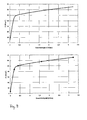
- FIG. 9 A diagram that outlines the relationship between the set speed and the power density.
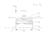
- FIG. 1 shows a coating system 1 according to the invention in a sectional view.
- an elongated cathode 3 is arranged with a length I and a width b, on which a target 4 is mounted.
- the cathode 3 lies in this view below the target 4 in the leaf level.
- cathode 3 and target 4 can also be embodied as an integrated component, ie the target material 4 can itself form the cathode 3.
- the cathode 3 is connected via a connecting line with the power supply 5.
- the electrical power can be coupled into the coating system 1 as direct current, alternating current, nonpolar pulsed current, bipolar pulsed current or radio frequency (RF) voltage.
- RF radio frequency
- FIG. 2 shows, as the coordinate system indicates at the top left, a lateral section of the coating system 1.
- a coating chamber 2 which is delimited by walls, a cathode 3 and the attached to the cathode 3 target material 4 are arranged.
- the target material 4 is facing a substrate plane 6, in which the substrates lie during the coating or along which the substrates are transported.
- the substrate plane 6 extends substantially parallel the target 4 with the underlying cathode 3.
- the target itself can form the cathode.
- the target 4 must always be at cathode potential.
- a magnet system 7 (for example consisting of yoke and magnet, not shown in detail) moves along the longitudinal direction of the cathode 3 or the target 4 at high speed, for example 1 m / s , The target 4 is scanned at high relative velocity v along the longitudinal extent I of the target 4.
- the magnet system can be driven on a carrier by a drive (not shown).
- the magnet system 7 is designed such that it generates a circumferential oval plasma channel 8 (race track) at a distance above the target surface.
- the plasma channel moves over the surface of the target 4 at the same speed v as the magnet system 7.
- the direction of movement is indicated by the arrow v.
- the high scanning speed prevents locally such a strong heating of the surface 4 'of the target 4 that can lead to surface effects such as melting of the target 4, local outgassing or chemical transformations of the compounds in the target 4.
- an arcing temperature-induced arc discharge
- a magnetron sputtering source according to the invention is in FIG. 3 shown.
- the surface 4 'of the target 4 points towards the substrate plane 6, the magnet system 7 faces away from the substrate plane.
- the target 4 may be cooled under certain circumstances.
- the magnet system 7 moves primarily at high speed in a direction perpendicular to the sheet plane (x-direction) relative to the target 4. However, superimposed movements in the y and z directions are also possible.
- a relative movement of the magnet system 7 to the target 4 means that either the magnetic field, for example, oscillates between the parallel shorter target edges in the x-direction.
- the target 4 can be driven relative to the magnet system 7 while the magnet system is firmly positioned in the coating chamber 2.
- An opposite movement of the magnet system 7 to the target 4 would be conceivable. In this case, for example, the target 4 could perform a rapid movement in the x-direction, while the magnet system 7 undergoes a superimposed movement in the y- and / or z-direction.
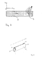
- FIG. 4 shows a plan view of a target 4 of a sputtering source according to the invention.
- movable magnets or magnet arrangements are arranged in the x-direction. These move at a speed as illustrated by arrows v, or a given velocity profile along a scan path.
- the arrow u indicates a superimposed counter-movement of the target 4, so that altogether in the x-direction a relative velocity u + v results.
- the magnets or magnet systems form plasma channels 8, 8 ', 8 "vertically above the target surface 4'. These plasma channels 8, 8 ', 8" move together with the magnet systems in the x direction at the velocities u + v relative to the target 4.
- the plasma channels 8, 8 'and 8 “have, for example, different closed configurations, eg an elongated oval (race track 8), a diamond-like shape 8', which does not extend over the entire width b of the target 4, and a bone-shaped surface 8". (each projected onto the target surface 4 ').
- the areas of the plasma channels 8, 8 'and 8 “are small compared to the entire scanned target surface 4' (both individually and the sum of the areas 8, 8 ', 8").
- an area ratio between the area of the target 4 and the area (s) of the plasma channel (s) 8 or 8 'and 8 is set much larger than 5.
- high relative velocities u + v in the x direction between the Magnetic system 7 and the target 4 for example, relative velocities greater than 1 m / s
- the high relative velocity u + v combined with the large area ratio, the temperature in the top atomic layers of the target 4 over conventional arrangements
- the better cooling makes it possible to use significantly higher power densities or sputtering rates without interfering surface effects, such as, for example, melting of the target or arcing.
- FIG. 4 is also exemplified at the plasma channel 8 an anode 9 shown, which runs in the area of the race track.
- the anode 9 moves, synchronously with the underlying under the cathode magnet system and thus with the plasma channel 8 at an absolute velocity v, that is, with a relative velocity u + v, over the target surface 4 '.
- Superposed to the target 4 and / or the magnet system can perform a relative movement in the y- and / or z-direction, so that a specific erosion profile is set specifically.
- FIG. 5 shows the FIG. 5 in a side sectional view.
- a cathode 3 is provided with target material 4, wherein the target surface 4 'is aligned with the substrate plane 6.
- the magnet system 7 which is movable at a speed v along the x-axis (as indicated at the top left in the figure). With the magnet system, the plasma channel or race track 8 also moves at a distance above the surface of the target 4. Of course, a multiplicity of further plasma channels can be moved in the region above the target surface 4 'in addition to the plasma channel 8 by a corresponding design of the magnet system 7. be formed.
- the plasma channel 8 extends in the projection over a region d along an entire region D of the target 4 (D corresponds here to the length I of the target).
- the area ratio between the total target surface and the surface of the plasma channel 8 (projected onto the surface of the target 4) is at least 15. This can also apply in particular to the ratio D / d.
- the area of the plasma channel can also be roughly equated with the area of the magnetic yoke, since these sizes are dimensioned substantially similar.
- one or more plasma channels (race tracks) 8 can be generated in an area above the target 4 between the target 4 and the substrate plane 6, which can be arranged next to or inside each other in the form of a pattern.
- the magnet arrangement 7 can be specifically designed such that a specific layer distribution and the erosion profile of the target 4 be optimized.
- an immovable with respect to the target 4 arranged anode assembly 9 is shown.
- the anode assembly 9 can in principle be formed either by the surroundings of the magnetron cathode 3 (for example, the chamber wall, a dark space frame, a circumferential profile, etc.). I'm in the FIG. 5
- the anode assembly 9 consists of a plurality of adjacent bars, which may be cooled or uncooled. These act punctually in the plasma channel 8 and are electrically connected with the movement of the magnet system 7.
- one or two electrodes 9 could be provided which move together with the magnet system 7 and are arranged along a plasma channel.
- a drive 10 for the magnet system 7 may be provided by a control device 11 for controlling the scan speed and / or the scan path and / or the power density (and thus the sputtering rate).
- the controller 11 may control the sputtering rate depending on, for example, the speed and / or location coordinates of the magnet system.
- FIG. 6 shows a further embodiment of the invention, wherein like elements are designated by the previously used reference numerals.
- the cathode 3 and the target 4 are segmented.
- the respective target segments in the region of the plasma channel 8 are at cathode potential, while the adjacent corresponding target segments act as the anode.
- the segments are indexed in this embodiment, together with the movement of the magnet system 7 and the plasma channel 8, corresponding to a speed v.
- the distance between the segments preferably corresponds to the dark space distance to electrical flashovers between adjacent Segments that are at different potential to avoid.
- the hint of the proportions in the FIG. 6 is purely schematic.
- the invention for a number of common sputtering processes can be used, for example, for sputtering with inert gas (argon, etc.), but also for sputtering processes with reactive gases (oxygen, nitrogen, NH 3 , etc.).
- inert gas argon, etc.
- reactive gases oxygen, nitrogen, NH 3 , etc.
- FIG. 7 a further sputtering source according to the invention is disclosed, which differs from the previous embodiments by an anode arrangement, which are arranged parallel to the direction of movement v of the magnet system 7 and the plasma channel 8.
- FIG. 8 shows a rotatable cathode within the scope of the invention.
- the increased relative velocity is characterized as the web velocity v on the surface of the target.
- the scanned target length corresponds here to the circumference.
- Cathode / target 3, 4 rotate about a central axis A.
- the racetrack 8 above the magnet system 7 is indicated in dashed lines.
- FIG. 9 shows a diagram (in two versions without or with measuring points) showing the dependence between the set speed and the maximum possible power density, ie the power density that can be supplied before the target surface melts before arcing occurs or before chemical changes within Enter the target surface, illustrated.
- a sharp increase in the possible power density is already evident at speeds of 0.1 m / s.
- the curve continues to increase at higher relative speeds, but at a lower slope (starting at between about 0.3 m / s and 0.4 m / s). Nevertheless, even in the higher speed ranges, an increase in speed still leads to significant increases in power density.
Landscapes
- Chemical & Material Sciences (AREA)
- Engineering & Computer Science (AREA)
- Physics & Mathematics (AREA)
- Plasma & Fusion (AREA)
- Analytical Chemistry (AREA)
- Chemical Kinetics & Catalysis (AREA)
- Materials Engineering (AREA)
- Mechanical Engineering (AREA)
- Metallurgy (AREA)
- Organic Chemistry (AREA)
- Physical Vapour Deposition (AREA)
Priority Applications (9)
| Application Number | Priority Date | Filing Date | Title |
|---|---|---|---|
| AT06124060T ATE499697T1 (de) | 2006-11-14 | 2006-11-14 | Magnetron-sputterquelle, sputter- beschichtungsanlage und verfahren zur beschichtung eines substrats |
| EP06124060.2A EP1923902B2 (fr) | 2006-11-14 | 2006-11-14 | Source de pulvérisation magnétron, système de revêtement par pulvérisation et procédé pour revêtir un substrat |
| DE502006008952T DE502006008952D1 (de) | 2006-11-14 | 2006-11-14 | Magnetron-Sputterquelle, Sputter-Beschichtungsanlage und Verfahren zur Beschichtung eines Substrats |
| TW096126427A TWI362428B (en) | 2006-11-14 | 2007-07-19 | Magnetron sputtering source, sputter-coating installation, and method for coating a substrate |
| KR1020070079124A KR100966671B1 (ko) | 2006-11-14 | 2007-08-07 | 마그네트론 스퍼터링 소스, 스퍼터-코팅 설비, 및 기판을코팅하는 방법 |
| US11/904,299 US20080173535A1 (en) | 2006-11-14 | 2007-09-24 | Magnetron Sputtering Source, Sputter-Coating Installation, and Method for Coating a Substrate |
| JP2007292802A JP5329795B2 (ja) | 2006-11-14 | 2007-11-12 | マグネトロンスパッタリング源、スパッタコーティング装置、及び基板コーティング方法 |
| CN2007101659923A CN101182631B (zh) | 2006-11-14 | 2007-11-14 | 磁控管溅射源、溅射涂敷设备及对衬底进行涂敷的方法 |
| KR1020100018485A KR20100029115A (ko) | 2006-11-14 | 2010-03-02 | 마그네트론 스퍼터링 소스, 스퍼터-코팅 설비, 및 기판을 코팅하는 방법 |
Applications Claiming Priority (1)
| Application Number | Priority Date | Filing Date | Title |
|---|---|---|---|
| EP06124060.2A EP1923902B2 (fr) | 2006-11-14 | 2006-11-14 | Source de pulvérisation magnétron, système de revêtement par pulvérisation et procédé pour revêtir un substrat |
Publications (3)
| Publication Number | Publication Date |
|---|---|
| EP1923902A1 true EP1923902A1 (fr) | 2008-05-21 |
| EP1923902B1 EP1923902B1 (fr) | 2011-02-23 |
| EP1923902B2 EP1923902B2 (fr) | 2014-07-23 |
Family
ID=37771100
Family Applications (1)
| Application Number | Title | Priority Date | Filing Date |
|---|---|---|---|
| EP06124060.2A Not-in-force EP1923902B2 (fr) | 2006-11-14 | 2006-11-14 | Source de pulvérisation magnétron, système de revêtement par pulvérisation et procédé pour revêtir un substrat |
Country Status (8)
| Country | Link |
|---|---|
| US (1) | US20080173535A1 (fr) |
| EP (1) | EP1923902B2 (fr) |
| JP (1) | JP5329795B2 (fr) |
| KR (2) | KR100966671B1 (fr) |
| CN (1) | CN101182631B (fr) |
| AT (1) | ATE499697T1 (fr) |
| DE (1) | DE502006008952D1 (fr) |
| TW (1) | TWI362428B (fr) |
Cited By (3)
| Publication number | Priority date | Publication date | Assignee | Title |
|---|---|---|---|---|
| DE102008009339A1 (de) * | 2008-02-14 | 2009-09-24 | Von Ardenne Anlagentechnik Gmbh | Verfahren zur Beschichtung mit leitfähigen und transparenten Zinkoxid-Schichten |
| GB2460456A (en) * | 2008-05-30 | 2009-12-02 | Mantis Deposition Ltd | Sputtering apparatus |
| CN113481478A (zh) * | 2021-06-23 | 2021-10-08 | 合肥联顿恪智能科技有限公司 | 一种溅射镀膜装置及成膜方法 |
Families Citing this family (20)
| Publication number | Priority date | Publication date | Assignee | Title |
|---|---|---|---|---|
| JP5296468B2 (ja) * | 2008-09-19 | 2013-09-25 | 富士フイルム株式会社 | 成膜方法及び成膜装置 |
| TWI391514B (zh) * | 2009-07-16 | 2013-04-01 | Univ Nat Sun Yat Sen | 磁控濺鍍機 |
| GB2473656A (en) * | 2009-09-21 | 2011-03-23 | Mantis Deposition Ltd | Sputter deposition using a cylindrical target |
| US9312108B2 (en) | 2013-03-01 | 2016-04-12 | Sputtering Components, Inc. | Sputtering apparatus |
| US9418823B2 (en) | 2013-03-01 | 2016-08-16 | Sputtering Components, Inc. | Sputtering apparatus |
| TWI489517B (zh) * | 2013-05-07 | 2015-06-21 | Univ Nat Taiwan | 表面處理裝置及方法 |
| CN103695858B (zh) * | 2013-12-26 | 2015-11-18 | 广东工业大学 | 一种用于刀具涂层沉积的多功能全自动离子镀膜机及其使用方法 |
| KR101419429B1 (ko) * | 2013-12-26 | 2014-07-14 | 주식회사 프로트 | 스퍼터 증착용 무빙장치 |
| KR102327285B1 (ko) * | 2014-02-20 | 2021-11-16 | 인테벡, 인코포레이티드 | 카운터웨이트를 이용하는 스퍼터링 시스템 및 방법 |
| EP2977202A1 (fr) * | 2014-07-25 | 2016-01-27 | AGC Glass Europe | Vitrage chauffant |
| US10811236B2 (en) | 2014-10-29 | 2020-10-20 | General Plasma, Inc. | Magnetic anode for sputter magnetron cathode |
| CN107208249B (zh) | 2015-02-03 | 2019-08-20 | 卡迪奈尔镀膜玻璃公司 | 包括气体分配系统的喷溅装置 |
| WO2016192814A1 (fr) * | 2015-06-05 | 2016-12-08 | Applied Materials, Inc. | Source de dépôt par pulvérisation cathodique, appareil de pulvérisation cathodique et son procédé de fonctionnement |
| CN107851548A (zh) * | 2015-07-24 | 2018-03-27 | 应用材料公司 | 热敏粘结的金属靶的冷却和利用优化 |
| TWI607482B (zh) * | 2016-01-08 | 2017-12-01 | Linco Technology Co Ltd | Interpolar target cathode device |
| EP3526810B1 (fr) * | 2016-10-14 | 2021-11-10 | Evatec AG | Source de pulvérisation |
| KR20190077575A (ko) * | 2016-11-22 | 2019-07-03 | 어플라이드 머티어리얼스, 인코포레이티드 | 기판 상으로의 층 증착을 위한 장치 및 방법 |
| CN111334770B (zh) * | 2020-04-07 | 2021-10-22 | 中国科学院近代物理研究所 | 一种弯弧加速器内壁镀膜装置及其磁控溅射镀膜方法 |
| JP7758441B2 (ja) * | 2021-06-17 | 2025-10-22 | 東京エレクトロン株式会社 | 成膜方法および成膜装置 |
| CN114032516B (zh) * | 2021-07-07 | 2023-12-22 | 重庆康佳光电科技有限公司 | 用于磁控溅射设备的磁源模组及磁控溅射设备 |
Citations (8)
| Publication number | Priority date | Publication date | Assignee | Title |
|---|---|---|---|---|
| US5106474A (en) * | 1990-11-21 | 1992-04-21 | Viratec Thin Films, Inc. | Anode structures for magnetron sputtering apparatus |
| EP0858095A2 (fr) * | 1997-02-06 | 1998-08-12 | Intevac, Inc. | Procédés et appareils pour pulvérisation magnétron à balayage linéaire |
| US6013159A (en) * | 1997-11-16 | 2000-01-11 | Applied Materials, Inc. | Particle trap in a magnetron sputtering chamber |
| EP1076352A2 (fr) * | 1999-08-12 | 2001-02-14 | Applied Materials, Inc. | Source de plasma à haute densité pour dépôt métallique ionisé |
| WO2001077402A2 (fr) * | 2000-04-07 | 2001-10-18 | Surface Engineered Products Corporation | Procede et appareil de pulverisation magnetron |
| US20050061666A1 (en) * | 2003-09-19 | 2005-03-24 | Subhadra Gupta | Linear sweeping magnetron sputtering cathode and scanning in-line system for arc-free reactive deposition and high target utilization |
| US20050103620A1 (en) * | 2003-11-19 | 2005-05-19 | Zond, Inc. | Plasma source with segmented magnetron cathode |
| DE102005019100A1 (de) * | 2005-04-25 | 2006-10-26 | Steag Hamatech Ag | Magnetsystem für eine Zerstäubungskathode |
Family Cites Families (24)
| Publication number | Priority date | Publication date | Assignee | Title |
|---|---|---|---|---|
| DD217964A3 (de) † | 1981-10-02 | 1985-01-23 | Ardenne Manfred | Einrichtung zum hochratezerstaeuben nach dem plasmatronprinzip |
| JPH06322534A (ja) * | 1993-05-07 | 1994-11-22 | Sharp Corp | 薄膜形成方法及び薄膜形成装置 |
| US5487822A (en) * | 1993-11-24 | 1996-01-30 | Applied Materials, Inc. | Integrated sputtering target assembly |
| JP3403550B2 (ja) † | 1995-06-29 | 2003-05-06 | 松下電器産業株式会社 | スパッタリング装置とスパッタリング方法 |
| US5855744A (en) * | 1996-07-19 | 1999-01-05 | Applied Komatsu Technology, Inc. | Non-planar magnet tracking during magnetron sputtering |
| JPH1143766A (ja) * | 1997-07-23 | 1999-02-16 | Matsushita Electric Ind Co Ltd | 薄膜形成方法及び装置 |
| EP0918351A1 (fr) * | 1997-11-19 | 1999-05-26 | Sinvaco N.V. | Magnétron planaire à ensemble d'aimants déplaçable |
| US6093293A (en) † | 1997-12-17 | 2000-07-25 | Balzers Hochvakuum Ag | Magnetron sputtering source |
| US6488824B1 (en) † | 1998-11-06 | 2002-12-03 | Raycom Technologies, Inc. | Sputtering apparatus and process for high rate coatings |
| US6365010B1 (en) * | 1998-11-06 | 2002-04-02 | Scivac | Sputtering apparatus and process for high rate coatings |
| US6031159A (en) * | 1998-12-10 | 2000-02-29 | Monsanto Corporation | Soybean cultivar 958088713716 |
| JP2001003166A (ja) * | 1999-04-23 | 2001-01-09 | Nippon Sheet Glass Co Ltd | 基体表面に被膜を被覆する方法およびその方法による基体 |
| DE69937948D1 (de) * | 1999-06-21 | 2008-02-21 | Bekaert Advanced Coatings N V | Magnetron mit beweglicher Magnetanordnung zur Kompensation des Erosionsprofils |
| US6402912B1 (en) * | 2000-11-09 | 2002-06-11 | Honeywell International Inc. | Sputtering target assembly |
| US6494999B1 (en) * | 2000-11-09 | 2002-12-17 | Honeywell International Inc. | Magnetron sputtering apparatus with an integral cooling and pressure relieving cathode |
| DE10145201C1 (de) † | 2001-09-13 | 2002-11-21 | Fraunhofer Ges Forschung | Einrichtung zum Beschichten von Substraten mit gekrümmter Oberfläche durch Pulsmagnetron-Zerstäuben |
| KR100446918B1 (ko) * | 2001-12-31 | 2004-09-01 | 엘지.필립스 엘시디 주식회사 | 촉매금속을 증착하기 위한 디씨 마그네트론 증착장비의 증착조건 |
| TW573041B (en) * | 2002-02-07 | 2004-01-21 | Hannstar Display Corp | Method for improving performance of sputtering target |
| DE10213043B4 (de) † | 2002-03-22 | 2008-10-30 | Von Ardenne Anlagentechnik Gmbh | Rohrmagnetron und seine Verwendung |
| JP2004010753A (ja) * | 2002-06-06 | 2004-01-15 | Konica Minolta Holdings Inc | 透明導電性フィルムの製造方法及び透明導電性フィルム |
| JP4246547B2 (ja) † | 2003-05-23 | 2009-04-02 | 株式会社アルバック | スパッタリング装置、及びスパッタリング方法 |
| US20060049040A1 (en) * | 2004-01-07 | 2006-03-09 | Applied Materials, Inc. | Apparatus and method for two dimensional magnetron scanning for sputtering onto flat panels |
| EP1626433B1 (fr) † | 2004-08-10 | 2007-02-21 | Applied Materials GmbH & Co. KG | Appareillage de pulvérisation magnétron, cathode cylindrique et méthod de depot des multicouches minces sur un substrat |
| WO2006063484A1 (fr) † | 2004-12-17 | 2006-06-22 | Unaxis Balzers Aktiengesellschaft | Appareil de pulverisation au magnetron |
-
2006
- 2006-11-14 AT AT06124060T patent/ATE499697T1/de active
- 2006-11-14 EP EP06124060.2A patent/EP1923902B2/fr not_active Not-in-force
- 2006-11-14 DE DE502006008952T patent/DE502006008952D1/de active Active
-
2007
- 2007-07-19 TW TW096126427A patent/TWI362428B/zh not_active IP Right Cessation
- 2007-08-07 KR KR1020070079124A patent/KR100966671B1/ko not_active Expired - Fee Related
- 2007-09-24 US US11/904,299 patent/US20080173535A1/en not_active Abandoned
- 2007-11-12 JP JP2007292802A patent/JP5329795B2/ja not_active Expired - Fee Related
- 2007-11-14 CN CN2007101659923A patent/CN101182631B/zh not_active Expired - Fee Related
-
2010
- 2010-03-02 KR KR1020100018485A patent/KR20100029115A/ko not_active Withdrawn
Patent Citations (8)
| Publication number | Priority date | Publication date | Assignee | Title |
|---|---|---|---|---|
| US5106474A (en) * | 1990-11-21 | 1992-04-21 | Viratec Thin Films, Inc. | Anode structures for magnetron sputtering apparatus |
| EP0858095A2 (fr) * | 1997-02-06 | 1998-08-12 | Intevac, Inc. | Procédés et appareils pour pulvérisation magnétron à balayage linéaire |
| US6013159A (en) * | 1997-11-16 | 2000-01-11 | Applied Materials, Inc. | Particle trap in a magnetron sputtering chamber |
| EP1076352A2 (fr) * | 1999-08-12 | 2001-02-14 | Applied Materials, Inc. | Source de plasma à haute densité pour dépôt métallique ionisé |
| WO2001077402A2 (fr) * | 2000-04-07 | 2001-10-18 | Surface Engineered Products Corporation | Procede et appareil de pulverisation magnetron |
| US20050061666A1 (en) * | 2003-09-19 | 2005-03-24 | Subhadra Gupta | Linear sweeping magnetron sputtering cathode and scanning in-line system for arc-free reactive deposition and high target utilization |
| US20050103620A1 (en) * | 2003-11-19 | 2005-05-19 | Zond, Inc. | Plasma source with segmented magnetron cathode |
| DE102005019100A1 (de) * | 2005-04-25 | 2006-10-26 | Steag Hamatech Ag | Magnetsystem für eine Zerstäubungskathode |
Cited By (3)
| Publication number | Priority date | Publication date | Assignee | Title |
|---|---|---|---|---|
| DE102008009339A1 (de) * | 2008-02-14 | 2009-09-24 | Von Ardenne Anlagentechnik Gmbh | Verfahren zur Beschichtung mit leitfähigen und transparenten Zinkoxid-Schichten |
| GB2460456A (en) * | 2008-05-30 | 2009-12-02 | Mantis Deposition Ltd | Sputtering apparatus |
| CN113481478A (zh) * | 2021-06-23 | 2021-10-08 | 合肥联顿恪智能科技有限公司 | 一种溅射镀膜装置及成膜方法 |
Also Published As
| Publication number | Publication date |
|---|---|
| KR100966671B1 (ko) | 2010-06-29 |
| DE502006008952D1 (de) | 2011-04-07 |
| CN101182631A (zh) | 2008-05-21 |
| ATE499697T1 (de) | 2011-03-15 |
| KR20080043689A (ko) | 2008-05-19 |
| CN101182631B (zh) | 2010-12-22 |
| JP2008121117A (ja) | 2008-05-29 |
| TWI362428B (en) | 2012-04-21 |
| EP1923902B2 (fr) | 2014-07-23 |
| KR20100029115A (ko) | 2010-03-15 |
| US20080173535A1 (en) | 2008-07-24 |
| EP1923902B1 (fr) | 2011-02-23 |
| JP5329795B2 (ja) | 2013-10-30 |
| TW200825197A (en) | 2008-06-16 |
Similar Documents
| Publication | Publication Date | Title |
|---|---|---|
| EP1923902B2 (fr) | Source de pulvérisation magnétron, système de revêtement par pulvérisation et procédé pour revêtir un substrat | |
| EP0603587B1 (fr) | Appareil de génération de plasma | |
| DE4412906C1 (de) | Verfahren und Einrichtung für die ionengestützte Vakuumbeschichtung | |
| DE3700633C1 (de) | Verfahren und Vorrichtung zum schonenden Beschichten elektrisch leitender Gegenstaends mittels Plasma | |
| EP2018653B1 (fr) | Source d'arc et arrangement d'aimants | |
| EP1042526A1 (fr) | Source de pulverisation au magnetron | |
| DE10084452B3 (de) | Lichtbogenquelle mit rechteckiger Kathode und Verfahren zur Lenkung eines Lichtbogenflecks | |
| EP0529259A1 (fr) | Appareil pour le traitement de substrats | |
| EP0725843A1 (fr) | Procede et systeme de vaporisation par bombardement electronique active au plasma | |
| EP1258026B1 (fr) | Procede de regulation de la densite d'un plasma ou de sa distribution dans une source de pulverisation au magnetron et source de pulverisation au magnetron | |
| EP1576641B1 (fr) | Source d'arc sous vide comprenant un dispositif de production de champ magnetique | |
| DE69732055T2 (de) | Vorrichtung zur Erzeugung eines Plasmas mit Entladung entlang einer magnetisch neutralen Linie | |
| WO2000016373A1 (fr) | Ensemble cible pour chambre d'evaporation par l'intermediaire d'un arc | |
| EP3900011B1 (fr) | Ensemble aimant conçu pour une source de plasma pour réaliser des traitement au plasma | |
| EP3900010B1 (fr) | Agencement d'électrodes pour une source de plasma pour exécuter des traitements de plasma | |
| DE102007051444B4 (de) | Verfahren und Vorrichtung zum Trockenätzen von kontinuierlich bewegten Materialien | |
| DE19610253A1 (de) | Zerstäubungseinrichtung | |
| EP2140475A2 (fr) | Anode pour la formation d'un plasma par création de décharges en arc électriques | |
| DE10234858A1 (de) | Einrichtung zur Erzeugung einer Magnetron-Entladung | |
| DE102012206553A1 (de) | Verfahren und Vorrichtung zum Steuern der Schichtdickenverteilung in einer Vakuumbeschichtung | |
| CH702969A2 (de) | Segmentierte Anode. | |
| EP3583619B1 (fr) | Évaporation par arc cathodique avec enlèvement de matière à la cathode prédéfini | |
| EP1473382A1 (fr) | Procédé et dispositif de déposition d'une couche activée par plasma par pulvérisation magnétron | |
| EP1462538B1 (fr) | Procédé de pulvérisation au magnétron réactif | |
| DE102010029690A1 (de) | Steuer- und/oder Regeleinrichtung, Steuerstrecke, Computerprogramm, computerlesbares Speichermedium und Verfahren des Herunterladens des Computerprogramms |
Legal Events
| Date | Code | Title | Description |
|---|---|---|---|
| PUAI | Public reference made under article 153(3) epc to a published international application that has entered the european phase |
Free format text: ORIGINAL CODE: 0009012 |
|
| 17P | Request for examination filed |
Effective date: 20061214 |
|
| AK | Designated contracting states |
Kind code of ref document: A1 Designated state(s): AT BE BG CH CY CZ DE DK EE ES FI FR GB GR HU IE IS IT LI LT LU LV MC NL PL PT RO SE SI SK TR |
|
| AX | Request for extension of the european patent |
Extension state: AL BA HR MK RS |
|
| AKX | Designation fees paid |
Designated state(s): AT BE BG CH CY CZ DE DK EE ES FI FR GB GR HU IE IS IT LI LT LU LV MC NL PL PT RO SE SI SK TR |
|
| GRAP | Despatch of communication of intention to grant a patent |
Free format text: ORIGINAL CODE: EPIDOSNIGR1 |
|
| GRAS | Grant fee paid |
Free format text: ORIGINAL CODE: EPIDOSNIGR3 |
|
| GRAA | (expected) grant |
Free format text: ORIGINAL CODE: 0009210 |
|
| AK | Designated contracting states |
Kind code of ref document: B1 Designated state(s): AT BE BG CH CY CZ DE DK EE ES FI FR GB GR HU IE IS IT LI LT LU LV MC NL PL PT RO SE SI SK TR |
|
| REG | Reference to a national code |
Ref country code: GB Ref legal event code: FG4D Free format text: NOT ENGLISH |
|
| REG | Reference to a national code |
Ref country code: CH Ref legal event code: EP |
|
| REG | Reference to a national code |
Ref country code: IE Ref legal event code: FG4D Free format text: LANGUAGE OF EP DOCUMENT: GERMAN |
|
| REF | Corresponds to: |
Ref document number: 502006008952 Country of ref document: DE Date of ref document: 20110407 Kind code of ref document: P |
|
| REG | Reference to a national code |
Ref country code: DE Ref legal event code: R096 Ref document number: 502006008952 Country of ref document: DE Effective date: 20110407 |
|
| REG | Reference to a national code |
Ref country code: NL Ref legal event code: VDEP Effective date: 20110223 |
|
| LTIE | Lt: invalidation of european patent or patent extension |
Effective date: 20110223 |
|
| PG25 | Lapsed in a contracting state [announced via postgrant information from national office to epo] |
Ref country code: PT Free format text: LAPSE BECAUSE OF FAILURE TO SUBMIT A TRANSLATION OF THE DESCRIPTION OR TO PAY THE FEE WITHIN THE PRESCRIBED TIME-LIMIT Effective date: 20110623 Ref country code: LV Free format text: LAPSE BECAUSE OF FAILURE TO SUBMIT A TRANSLATION OF THE DESCRIPTION OR TO PAY THE FEE WITHIN THE PRESCRIBED TIME-LIMIT Effective date: 20110223 Ref country code: ES Free format text: LAPSE BECAUSE OF FAILURE TO SUBMIT A TRANSLATION OF THE DESCRIPTION OR TO PAY THE FEE WITHIN THE PRESCRIBED TIME-LIMIT Effective date: 20110603 Ref country code: LT Free format text: LAPSE BECAUSE OF FAILURE TO SUBMIT A TRANSLATION OF THE DESCRIPTION OR TO PAY THE FEE WITHIN THE PRESCRIBED TIME-LIMIT Effective date: 20110223 Ref country code: SE Free format text: LAPSE BECAUSE OF FAILURE TO SUBMIT A TRANSLATION OF THE DESCRIPTION OR TO PAY THE FEE WITHIN THE PRESCRIBED TIME-LIMIT Effective date: 20110223 Ref country code: GR Free format text: LAPSE BECAUSE OF FAILURE TO SUBMIT A TRANSLATION OF THE DESCRIPTION OR TO PAY THE FEE WITHIN THE PRESCRIBED TIME-LIMIT Effective date: 20110524 |
|
| PG25 | Lapsed in a contracting state [announced via postgrant information from national office to epo] |
Ref country code: NL Free format text: LAPSE BECAUSE OF FAILURE TO SUBMIT A TRANSLATION OF THE DESCRIPTION OR TO PAY THE FEE WITHIN THE PRESCRIBED TIME-LIMIT Effective date: 20110223 Ref country code: CY Free format text: LAPSE BECAUSE OF FAILURE TO SUBMIT A TRANSLATION OF THE DESCRIPTION OR TO PAY THE FEE WITHIN THE PRESCRIBED TIME-LIMIT Effective date: 20110223 Ref country code: FI Free format text: LAPSE BECAUSE OF FAILURE TO SUBMIT A TRANSLATION OF THE DESCRIPTION OR TO PAY THE FEE WITHIN THE PRESCRIBED TIME-LIMIT Effective date: 20110223 Ref country code: SI Free format text: LAPSE BECAUSE OF FAILURE TO SUBMIT A TRANSLATION OF THE DESCRIPTION OR TO PAY THE FEE WITHIN THE PRESCRIBED TIME-LIMIT Effective date: 20110223 Ref country code: BG Free format text: LAPSE BECAUSE OF FAILURE TO SUBMIT A TRANSLATION OF THE DESCRIPTION OR TO PAY THE FEE WITHIN THE PRESCRIBED TIME-LIMIT Effective date: 20110523 |
|
| REG | Reference to a national code |
Ref country code: IE Ref legal event code: FD4D |
|
| PG25 | Lapsed in a contracting state [announced via postgrant information from national office to epo] |
Ref country code: EE Free format text: LAPSE BECAUSE OF FAILURE TO SUBMIT A TRANSLATION OF THE DESCRIPTION OR TO PAY THE FEE WITHIN THE PRESCRIBED TIME-LIMIT Effective date: 20110223 Ref country code: DK Free format text: LAPSE BECAUSE OF FAILURE TO SUBMIT A TRANSLATION OF THE DESCRIPTION OR TO PAY THE FEE WITHIN THE PRESCRIBED TIME-LIMIT Effective date: 20110223 Ref country code: IE Free format text: LAPSE BECAUSE OF FAILURE TO SUBMIT A TRANSLATION OF THE DESCRIPTION OR TO PAY THE FEE WITHIN THE PRESCRIBED TIME-LIMIT Effective date: 20110223 |
|
| PLBI | Opposition filed |
Free format text: ORIGINAL CODE: 0009260 |
|
| PG25 | Lapsed in a contracting state [announced via postgrant information from national office to epo] |
Ref country code: SK Free format text: LAPSE BECAUSE OF FAILURE TO SUBMIT A TRANSLATION OF THE DESCRIPTION OR TO PAY THE FEE WITHIN THE PRESCRIBED TIME-LIMIT Effective date: 20110223 Ref country code: CZ Free format text: LAPSE BECAUSE OF FAILURE TO SUBMIT A TRANSLATION OF THE DESCRIPTION OR TO PAY THE FEE WITHIN THE PRESCRIBED TIME-LIMIT Effective date: 20110223 Ref country code: RO Free format text: LAPSE BECAUSE OF FAILURE TO SUBMIT A TRANSLATION OF THE DESCRIPTION OR TO PAY THE FEE WITHIN THE PRESCRIBED TIME-LIMIT Effective date: 20110223 |
|
| 26 | Opposition filed |
Opponent name: VON ARDENNE ANLAGENTECHNIK GMBH Effective date: 20111123 |
|
| PLAX | Notice of opposition and request to file observation + time limit sent |
Free format text: ORIGINAL CODE: EPIDOSNOBS2 |
|
| REG | Reference to a national code |
Ref country code: DE Ref legal event code: R026 Ref document number: 502006008952 Country of ref document: DE Effective date: 20111123 |
|
| PG25 | Lapsed in a contracting state [announced via postgrant information from national office to epo] |
Ref country code: PL Free format text: LAPSE BECAUSE OF FAILURE TO SUBMIT A TRANSLATION OF THE DESCRIPTION OR TO PAY THE FEE WITHIN THE PRESCRIBED TIME-LIMIT Effective date: 20110223 |
|
| PLBB | Reply of patent proprietor to notice(s) of opposition received |
Free format text: ORIGINAL CODE: EPIDOSNOBS3 |
|
| BERE | Be: lapsed |
Owner name: APPLIED MATERIALS, INC. Effective date: 20111130 |
|
| PG25 | Lapsed in a contracting state [announced via postgrant information from national office to epo] |
Ref country code: IT Free format text: LAPSE BECAUSE OF FAILURE TO SUBMIT A TRANSLATION OF THE DESCRIPTION OR TO PAY THE FEE WITHIN THE PRESCRIBED TIME-LIMIT Effective date: 20110223 |
|
| PG25 | Lapsed in a contracting state [announced via postgrant information from national office to epo] |
Ref country code: MC Free format text: LAPSE BECAUSE OF NON-PAYMENT OF DUE FEES Effective date: 20111130 |
|
| REG | Reference to a national code |
Ref country code: CH Ref legal event code: PL |
|
| GBPC | Gb: european patent ceased through non-payment of renewal fee |
Effective date: 20111114 |
|
| PG25 | Lapsed in a contracting state [announced via postgrant information from national office to epo] |
Ref country code: LI Free format text: LAPSE BECAUSE OF NON-PAYMENT OF DUE FEES Effective date: 20111130 Ref country code: CH Free format text: LAPSE BECAUSE OF NON-PAYMENT OF DUE FEES Effective date: 20111130 |
|
| REG | Reference to a national code |
Ref country code: FR Ref legal event code: ST Effective date: 20120731 |
|
| PG25 | Lapsed in a contracting state [announced via postgrant information from national office to epo] |
Ref country code: BE Free format text: LAPSE BECAUSE OF NON-PAYMENT OF DUE FEES Effective date: 20111130 |
|
| PG25 | Lapsed in a contracting state [announced via postgrant information from national office to epo] |
Ref country code: GB Free format text: LAPSE BECAUSE OF NON-PAYMENT OF DUE FEES Effective date: 20111114 |
|
| REG | Reference to a national code |
Ref country code: DE Ref legal event code: R082 Ref document number: 502006008952 Country of ref document: DE Representative=s name: LERMERRAIBLE GBR PATENT- UND RECHTSANWAELTE, DE Ref country code: DE Ref legal event code: R082 Ref document number: 502006008952 Country of ref document: DE Representative=s name: ZIMMERMANN & PARTNER, DE Ref country code: DE Ref legal event code: R082 Ref document number: 502006008952 Country of ref document: DE Representative=s name: ZIMMERMANN & PARTNER PATENTANWAELTE MBB, DE |
|
| REG | Reference to a national code |
Ref country code: DE Ref legal event code: R082 Ref document number: 502006008952 Country of ref document: DE Representative=s name: ZIMMERMANN & PARTNER, DE Ref country code: DE Ref legal event code: R082 Ref document number: 502006008952 Country of ref document: DE Representative=s name: ZIMMERMANN & PARTNER PATENTANWAELTE MBB, DE |
|
| PG25 | Lapsed in a contracting state [announced via postgrant information from national office to epo] |
Ref country code: FR Free format text: LAPSE BECAUSE OF NON-PAYMENT OF DUE FEES Effective date: 20111130 |
|
| REG | Reference to a national code |
Ref country code: AT Ref legal event code: MM01 Ref document number: 499697 Country of ref document: AT Kind code of ref document: T Effective date: 20111114 |
|
| PG25 | Lapsed in a contracting state [announced via postgrant information from national office to epo] |
Ref country code: AT Free format text: LAPSE BECAUSE OF NON-PAYMENT OF DUE FEES Effective date: 20111114 |
|
| PG25 | Lapsed in a contracting state [announced via postgrant information from national office to epo] |
Ref country code: LU Free format text: LAPSE BECAUSE OF NON-PAYMENT OF DUE FEES Effective date: 20111114 |
|
| PG25 | Lapsed in a contracting state [announced via postgrant information from national office to epo] |
Ref country code: IS Free format text: LAPSE BECAUSE OF FAILURE TO SUBMIT A TRANSLATION OF THE DESCRIPTION OR TO PAY THE FEE WITHIN THE PRESCRIBED TIME-LIMIT Effective date: 20110223 |
|
| PG25 | Lapsed in a contracting state [announced via postgrant information from national office to epo] |
Ref country code: TR Free format text: LAPSE BECAUSE OF FAILURE TO SUBMIT A TRANSLATION OF THE DESCRIPTION OR TO PAY THE FEE WITHIN THE PRESCRIBED TIME-LIMIT Effective date: 20110223 |
|
| PG25 | Lapsed in a contracting state [announced via postgrant information from national office to epo] |
Ref country code: HU Free format text: LAPSE BECAUSE OF FAILURE TO SUBMIT A TRANSLATION OF THE DESCRIPTION OR TO PAY THE FEE WITHIN THE PRESCRIBED TIME-LIMIT Effective date: 20110223 |
|
| PUAH | Patent maintained in amended form |
Free format text: ORIGINAL CODE: 0009272 |
|
| STAA | Information on the status of an ep patent application or granted ep patent |
Free format text: STATUS: PATENT MAINTAINED AS AMENDED |
|
| 27A | Patent maintained in amended form |
Effective date: 20140723 |
|
| AK | Designated contracting states |
Kind code of ref document: B2 Designated state(s): AT BE BG CH CY CZ DE DK EE ES FI FR GB GR HU IE IS IT LI LT LU LV MC NL PL PT RO SE SI SK TR |
|
| REG | Reference to a national code |
Ref country code: DE Ref legal event code: R102 Ref document number: 502006008952 Country of ref document: DE |
|
| REG | Reference to a national code |
Ref country code: DE Ref legal event code: R102 Ref document number: 502006008952 Country of ref document: DE Effective date: 20140723 |
|
| PGFP | Annual fee paid to national office [announced via postgrant information from national office to epo] |
Ref country code: DE Payment date: 20141119 Year of fee payment: 9 |
|
| PG25 | Lapsed in a contracting state [announced via postgrant information from national office to epo] |
Ref country code: LV Free format text: LAPSE BECAUSE OF FAILURE TO SUBMIT A TRANSLATION OF THE DESCRIPTION OR TO PAY THE FEE WITHIN THE PRESCRIBED TIME-LIMIT Effective date: 20140723 |
|
| REG | Reference to a national code |
Ref country code: DE Ref legal event code: R119 Ref document number: 502006008952 Country of ref document: DE |
|
| PG25 | Lapsed in a contracting state [announced via postgrant information from national office to epo] |
Ref country code: DE Free format text: LAPSE BECAUSE OF NON-PAYMENT OF DUE FEES Effective date: 20160601 |