EP1920449B1 - Tastaturanordnung - Google Patents
Tastaturanordnung Download PDFInfo
- Publication number
- EP1920449B1 EP1920449B1 EP06791677A EP06791677A EP1920449B1 EP 1920449 B1 EP1920449 B1 EP 1920449B1 EP 06791677 A EP06791677 A EP 06791677A EP 06791677 A EP06791677 A EP 06791677A EP 1920449 B1 EP1920449 B1 EP 1920449B1
- Authority
- EP
- European Patent Office
- Prior art keywords
- snap
- plate
- action disc
- disc
- arrangement according
- Prior art date
- Legal status (The legal status is an assumption and is not a legal conclusion. Google has not performed a legal analysis and makes no representation as to the accuracy of the status listed.)
- Not-in-force
Links
Images


Classifications
-
- H—ELECTRICITY
- H01—ELECTRIC ELEMENTS
- H01H—ELECTRIC SWITCHES; RELAYS; SELECTORS; EMERGENCY PROTECTIVE DEVICES
- H01H13/00—Switches having rectilinearly-movable operating part or parts adapted for pushing or pulling in one direction only, e.g. push-button switch
- H01H13/70—Switches having rectilinearly-movable operating part or parts adapted for pushing or pulling in one direction only, e.g. push-button switch having a plurality of operating members associated with different sets of contacts, e.g. keyboard
- H01H13/702—Switches having rectilinearly-movable operating part or parts adapted for pushing or pulling in one direction only, e.g. push-button switch having a plurality of operating members associated with different sets of contacts, e.g. keyboard with contacts carried by or formed from layers in a multilayer structure, e.g. membrane switches
- H01H13/705—Switches having rectilinearly-movable operating part or parts adapted for pushing or pulling in one direction only, e.g. push-button switch having a plurality of operating members associated with different sets of contacts, e.g. keyboard with contacts carried by or formed from layers in a multilayer structure, e.g. membrane switches characterised by construction, mounting or arrangement of operating parts, e.g. push-buttons or keys
-
- H—ELECTRICITY
- H01—ELECTRIC ELEMENTS
- H01H—ELECTRIC SWITCHES; RELAYS; SELECTORS; EMERGENCY PROTECTIVE DEVICES
- H01H13/00—Switches having rectilinearly-movable operating part or parts adapted for pushing or pulling in one direction only, e.g. push-button switch
- H01H13/02—Details
- H01H13/26—Snap-action arrangements depending upon deformation of elastic members
- H01H13/48—Snap-action arrangements depending upon deformation of elastic members using buckling of disc springs
-
- H—ELECTRICITY
- H01—ELECTRIC ELEMENTS
- H01H—ELECTRIC SWITCHES; RELAYS; SELECTORS; EMERGENCY PROTECTIVE DEVICES
- H01H2205/00—Movable contacts
- H01H2205/016—Separate bridge contact
- H01H2205/024—Means to facilitate positioning
- H01H2205/03—Apertured plate
-
- H—ELECTRICITY
- H01—ELECTRIC ELEMENTS
- H01H—ELECTRIC SWITCHES; RELAYS; SELECTORS; EMERGENCY PROTECTIVE DEVICES
- H01H2205/00—Movable contacts
- H01H2205/032—Several contacts formed in one plate or layer
-
- H—ELECTRICITY
- H01—ELECTRIC ELEMENTS
- H01H—ELECTRIC SWITCHES; RELAYS; SELECTORS; EMERGENCY PROTECTIVE DEVICES
- H01H2215/00—Tactile feedback
- H01H2215/004—Collapsible dome or bubble
-
- H—ELECTRICITY
- H01—ELECTRIC ELEMENTS
- H01H—ELECTRIC SWITCHES; RELAYS; SELECTORS; EMERGENCY PROTECTIVE DEVICES
- H01H2227/00—Dimensions; Characteristics
- H01H2227/002—Layer thickness
-
- H—ELECTRICITY
- H01—ELECTRIC ELEMENTS
- H01H—ELECTRIC SWITCHES; RELAYS; SELECTORS; EMERGENCY PROTECTIVE DEVICES
- H01H2227/00—Dimensions; Characteristics
- H01H2227/026—Separate dome contact
-
- H—ELECTRICITY
- H01—ELECTRIC ELEMENTS
- H01H—ELECTRIC SWITCHES; RELAYS; SELECTORS; EMERGENCY PROTECTIVE DEVICES
- H01H2229/00—Manufacturing
- H01H2229/02—Laser
-
- H—ELECTRICITY
- H01—ELECTRIC ELEMENTS
- H01H—ELECTRIC SWITCHES; RELAYS; SELECTORS; EMERGENCY PROTECTIVE DEVICES
- H01H2239/00—Miscellaneous
- H01H2239/004—High frequency adaptation or shielding
Definitions
- the invention is concerned with keyboard assemblies which, prior to or during the manufacture of, for example, an electrical contact, by actuation of a button provided in the keyboard assembly, indicate to the user, by a tactile "switching click", the induction of the desired contact. Release the button and return it to its original position.
- keyboard assemblies which, prior to or during the manufacture of, for example, an electrical contact, by actuation of a button provided in the keyboard assembly, indicate to the user, by a tactile "switching click", the induction of the desired contact. Release the button and return it to its original position.
- Such keyboard arrangements are widely used and are used for example in remote controls for devices of the entertainment industry or in telephones.
- This "peeling crack”, which is also referred to as a pressure point, is generally realized by arranging a so-called snap disk below the respective knob.
- a snap-action disc is essentially arched components of metal or plastic which have a non-linear spring characteristic and which span a space, the head resting in its initial position on the zenith surface of the curved component. If a force acts on the button to trigger an electrical contact, the snap disc is elastically deformed by flattening the curvature. In doing so, the force required to flatten the snap disc increases slightly, and when the curl is pressed approximately flat, becomes smaller than the force needed to flatten it.
- the spring direction of the snap disc reverses, whereby the force acting in this moment is less than the force required to flatten the curvature.
- the interaction of high and low actuation force or the reversal of the spring direction is then perceived by a user as a tactile feedback for triggering, for example, an electrical contact. If, in the flattened state, the force no longer acts on the button, it is returned to its original position by the elastic deformation of the snap-action disc.
- the flattening of the snap disc also causes a slight increase in its outer diameter. If this enlargement is prevented or even suppressed, there is a risk that the snap disc will not return to its original position.
- a plate is present, which has a plurality of openings and that this plate is arranged at a small distance above a board, wherein below each breakthrough on the board two mutually insulated contact surfaces are present.
- a snap disc is arranged in each of these openings, which connects under the action of a force on the knob, the two contact surfaces for making an electrical contact.
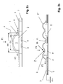
- the respective snap disk 1 centrally disposed within a breakthrough 2 a plate 3 and the resulting due to the cross-sectional proportions of snap disk 1 and breakthrough 2 resulting radial distance with a suitable plastic material 4, whereby the snap disk 1 formed of metal elastically in the respective breakthrough is suspended.
- this technology is very expensive, since on the one hand the plate with the openings and the snap discs must be formed for example by punching and / or cutting and connected by means of another step, which does not belong to metal processing.
- a snap disk arrangement in which a formed of metal and having a curvature snap disc rests with its edge regions on a base formed of insulating material and covers a formed in the base cavity. Within the cavity there is disposed an electrical contact surface which comes into physical contact with the snap-action disc when the buckling of the snap-action disc is pressed downwards in the direction of the cavity.
- the invention is therefore based on the object of specifying a keyboard arrangement which, in addition to high flexibility in the production and design changes, also forms a complete shield against high-frequency radiation.
- domes and the plates are made individually, these components can be manufactured with relatively simple punching and embossing tools and are very easily connected to complex units, for example by laser welding.
- the domes for a variety of applications can be made with one and the same set of tools, a very high degree of standardization is achieved. Since the diameter of the snap discs is always larger than the clear cross sections of the openings, it is ensured that the keyboard assembly according to the invention ensures complete shielding against unwanted frequencies by the complete coverage or the closure of the respective breakthrough with a snap disc, which are arranged from below the plate electrical components are emitted or act on these.
- the snap discs and the webs integrally connected to them made of metal or metallized plastic and electrically conductive with the plate be connected.
- the formation of the arranged below the keyboard assembly electrical contacts per snap disk can be limited to a contact element.
- a reduction of the components is ensured according to claim 3, characterized in that at least two of a plurality of snap discs are connected by means of a common web to the plate. Depending on the design of the webs, it is also possible to form all the domes of a keyboard assembly in one piece.
- each snap disc is fixedly connected by means of at least two webs with the plate, wherein each web used for stationary connection with the plate is provided with a hinge.
- each web used for stationary connection with the plate is provided with a hinge.
- the snap disc according to claim 7 has a convex bead on its zenith surface, the curvature of which extends into the space spanned by the curvature of the snap disc, even large distances between the zenith surface and the contact surface (s) on the printed circuit board can be overcome.
- the circuit board or conductor foil projects at least into the spaces that are surrounded by the openings.
- a first embodiment of the keyboard assembly according to the invention is shown in its initial position.
- This keyboard assembly has a domed snap-action disc 1 made of metal, which is formed dome-shaped and spans the underlying space 5.
- This snap-action disc 1 is integrally connected to a web 6.
- a metal plate 3 is also provided, which has an opening 2.
- the snap-action disc 1 is connected to the plate 3 only by means of the single web 6 by Lasersch adoptedung X.
- a printed circuit board 7 is shown, on which two electrical contact surfaces 8, 9 are arranged. Only for the sake of completeness, it should be noted that the in Fig. 2a shown mutual distance between the plate 3 and the circuit board 7 need not necessarily be present, but only for the sake of better illustration in Fig. 2a has been recorded.
- the diameter D1 of the snap-action disc 1 is greater than the clear cross-section D2 of the opening 2. This ensures that in each position of the snap disc 1 together with the plate 3 components in the direction of arrow P1 below the plate 3 and the snap disc 1 are arranged, shields.
- the mutual distance between the contact surfaces 8, 9 or the printed circuit board 7 and the snap-action disk 1 is adjusted so that the deformed snap-action disk 1 rests against the contact surfaces 8, 9 or an electrically conductive connection is established between the contact surfaces 8, 9, when the "switching crack" is heard, the user receives with the "switching crack” a tangible confirmation that his keystroke has also led to the desired switching command.
- FIG. 2b Another embodiment of the breakthrough 2 covering the snap disk 1 is shown. Just like the in Fig. 2a shown snap disk 1 also vaulted the snap disk according to Fig. 2b the breakthrough 2 completely. However, since often the plate 3 must be made relatively thick to produce a suitable shield, it may happen that one according to Fig. 2a merely dome-shaped snap-action disc 1 in the production of an electrical contact already generates the "switching crack", although no electrical contact has been made. Therefore, the snap disk 1 according to Fig. 2b provided on its zenith surface Z with a curved bead 10, the curvature of which extends into the space 5, which is spanned by the snap disk 1.
- the desired "switching crack” can be adjusted very flexibly and quickly to a given geometry of printed circuit board 7 and plate 3 by simply changing the ridge depth of the bead 10 in the space 5.
- Fig. 2b removable, that only a contact surface 8 'is arranged on the circuit board 7.
- the snap disk 1 In order to initiate an electrical contact with only one contact surface 8 ', when the snap disk 1 comes into physical contact with the contact surface 8', it is necessary for the snap disk 1 to lie “on ground”. Since the snap disk 1 according to Fig. 2b formed of metal and connected to the plate 3, which is also made of metal, this is solved in the present case, that in the embodiment according to Fig. 2b the plate 3 is "on ground".
- the circuit board 7 may be formed as a conductor foil.
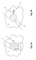
- FIG. 2b shows Fig. 2b another snap-action disc 1 ', which is juxtaposed to the snap-action disc 1, and which, like the snap-action disc 1, is capable of producing a "switching crack” to create.
- this snap disk 1 ' is not used for generating a "switching crack” when performing an electrical contact, but only serves the shielding of a component 12 on the circuit board 7, which protrudes because of its height from the plate 3.
- the two snap discs 1 and 1 ' are connected by means of a common web 6 by laser welding X.
- two snap disks 1, which are each arranged above contact surfaces 8 ' can also be connected to the plate 3 by means of a common web 6. In such a case would be in Fig. 2b or 6, the component 11 is replaced by at least one contact surface 8 '.
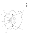
- Fig. 3b is shown another form of the web 6, with which the snap disc 1 is connected to the plate 3.
- the jaw forms a hinge 11.
- the webs 6, as in Fig. 3b and Fig. 4 shown near its free ends to the plate 3 by laser welding X connected.
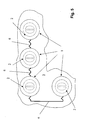
- Fig. 5 a combination of four snap discs 1 is shown, which are arranged above corresponding openings 2. All four snap discs 1 are integrally connected to each other via common webs 6 and can therefore be made in a punching pass.
- Fig. 7 instead of a printed circuit board 7, a conductor foil 7 'available.
- the conductor foil 7' projects into the space 12, which is bordered by the opening 2.
- Fig. 7 added that the execution according to Fig. 7 not necessarily conductor foils 7 'required and that the bead 10 shown in another embodiment of Fig. 7 can also be completely eliminated.
- the apertures 2 should be conical in order to reduce wear.
Landscapes
- Push-Button Switches (AREA)
- Input From Keyboards Or The Like (AREA)
Description
- Die Erfindung befasst sich mit Tastaturanordnungen, die vor oder bei der Herstellung beispielsweise eines elektrischen Kontakts durch Betätigung eines in der Tastaturanordnung vorhandenen Knopfes dem Benutzer durch einen fühlbaren "Schaltknack" die Herbeiführung des gewünschten Kontakts anzeigen und beim. Loslassen des Knopfes diesen wieder in seine Ausgangsposition verbringt. Derartige Tastaturanordnungen sind weit verbreitet und werden beispielsweise in Fernbedienungen für Geräte der Unterhaltungsindustrie oder auch in Telefonen verwendet.
- Dieser "Schältknack", welcher auch als Druckpunkt bezeichnet wird, wird allgemein dadurch realisiert, dass unterhalb des jeweiligen Knopfes eine sogenannte Schnappscheibe angeordnet ist. Bei einer Schnappscheibe handelt es sich im Wesentlichen um gewölbt ausgebildete Bauelemente aus Metall oder Kunststoff, die eine nichtlineare Federkennlinie haben und die einen Raum überspannen, wobei der Kopf in seiner Ausgangsposition an der Zenitfläche des gewölbten Bauteils anliegt. Wirkt nun eine Kraft auf den Knopf, um einen elektrischen Kontakt auszulösen, wird die Schnappscheibe elastisch verformt, indem die Wölbung abgeplattet wird. Dabei nimmt die Kraft, die zum Abplatten der Schnappscheibe erforderlich ist, leicht zu und wird dann, wenn die Wölbung annähernd flach gedrückt ist, kleiner als Kraft, die zum Abplatten erforderlich ist. Ist die Wölbung der Schnappscheibe weitgehend abgeplattet, kehrt sich die Federrichtung der Schnappscheibe um, wobei auch die in diesem Moment wirkende Kraft geringer ist als die Kraft, die zum Abplatten der Wölbung erforderlich ist. Das Zusammenspiel von hoher und geringer Betätigungskraft bzw. die Umkehr der Federrichtung wird dann von einem Benutzer als taktile Rückmeldung für die Auslösung beispielsweise eines elektrischen Kontakts empfunden. Wirkt im abgeplatteten Zustand die Kraft nicht mehr auf den Knopf, wird dieser durch die elastische Verformung der Schnappscheibe wieder in seine Ausgangsposition zurück verbracht. Wie leicht einzusehen ist, bewirkt die Abplattung der Schnappscheibe auch eine geringfügige Vergrößerung ihres Außendurchmessers. Wird diese Vergrößerung verhindert oder gar unterdrückt, besteht die Gefahr, dass die Schnappscheibe nicht mehr in ihre Ausgangslage zurückkehrt.
- Um Tastaturen unter Verwendung von Schnappscheiben zu bilden, haben sich im Wesentlichen zwei Technologien herausgebildet. Diesen Technologien ist gemein, dass eine Platte vorhanden ist, die eine Mehrzahl von Durchbrüchen aufweist und dass diese Platte mit geringem Abstand oberhalb eine Platine angeordnet ist, wobei unterhalb eines jeden Durchbruchs auf der Platine zwei von einander isolierte Kontaktflächen vorhanden sind. Außerdem ist in jedem dieser Durchbrüche eine Schnappscheibe angeordnet, die unter Wirkung einer Kraft auf den Knopf die beiden Kontaktflächen zur Herstellung eines elektrischen Kontakts verbindet.
- Zur Herstellung der Verbindung der Schnappscheibe wird gemäß der einen in
Fig. 1 gezeigten Technologie die jeweilige Schnappscheibe 1 zentrisch innerhalb eines Durchbruchs 2 einer Platte 3 angeordnet und der sich aufgrund der Querschnittsverhältnisse von Schnappscheibe 1 und Durchbruch 2 ergebende gegenseitig radiale Abstand mit einem geeigneten Kunststoffmaterial 4 ausgefüllt, wodurch die aus Metall gebildete Schnappscheibe 1 elastisch im jeweiligen Durchbruch 3 aufgehängt ist. Wie leicht einzusehen ist, ist diese Technologie sehr aufwendig, da zum einen die Platte mit den Durchbrüchen und die Schnappscheiben beispielsweise durch Stanzen und/oder Schneiden gebildet werden müssen und mittels eines weiteren Arbeitsschrittes, der nicht zur Metallverarbeitung gehört, verbunden werden müssen. - Zur Verringerung dieses Aufwandes ist beispielsweise aus
US 4 343 973 eine Schnappscheibenanordnung bekannt, bei welcher eine aus Metall gebildete und eine Wölbung aufweisende Schnappscheibe mit ihren Randbereichen auf einer aus Isoliermaterial gebildeten Unterlage aufliegt und einen in der Unterlage ausgebildeten Hohlraum überdeckt. Innerhalb des Hohlraums ist eine elektrische Kontaktfläche angeordnet, die mit der Schnappscheibe in körperlichen Kontakt kommt, wenn die Wölbung der Schnappscheibe nach unten, in Richtung des Hohlraums gedrückt wird. - Deshalb ist man gemäß der anderen bekannten Technologie dazu übergegangen, die Schnappscheibenanordnung nicht mehr aus verschiedenen Komponenten aufzubauen, sondern die Platte mit samt den Schnappscheiben einstückig aus Metall zu bilden, indem entsprechende Stanz- und Prägeschritte angewendet werden. Hierzu sei beispielsweise auf
DE 19851534 undDE 3618131 verwiesen. Um die notwendige elastische Aufhängung der Schnappscheiben in der Platte zu gewährleisten sowie auch einen genügend großen Freiraum für die radiale Ausdehnung der jeweiligen Schnappscheibe unter dem Druck des betätigten Knopfes bereitzustellen, sind entsprechend große Freischnitte um die Schnappscheibe herum erforderlich. Bei dieser Technologie wird neben der Komplexität solcher, die einstückige Ausbildung von entsprechenden Tastaturanordnungen erlaubenden Stanzwerkzeuge auch als nachteilig erachtet, dass jede Designänderung neue Stanzwerkzeuge erforderlich macht. - Zur Herstellung der EMV Kriterien bzw. zur Gewährleistung einer genügenden Abschirmung gegenüber hoch-frequenter Strahlung sind aber derartig große Freischnitte oder radiale Abstände zwischen Durchbrüchen und Schnappscheiben auch dann nicht tolerabel, wenn die jeweiligen Freiräume mit Kunststoff ausgefüllt sind.
- Daher liegt der Erfindung die Aufgabe zugrunde, eine Tastaturanordnung anzugeben, die neben einer hohen Flexibilität bei der Herstellung und Designänderungen auch eine vollständige Abschirmung gegenüber hoch-frequenter Strahlung bildet.
- Diese Aufgabe wird mit den in Anspruch 1 angegebenen Merkmalen gelöst. Dadurch, dass die Schnappscheiben und die Platten einzeln gefertigt werden, können diese Komponenten mit vergleichsweise einfachen Stanz- und Prägwerkzeugen gefertigt werden und zu komplexeren Einheiten sehr einfach beispielsweise durch Laserschweißen verbunden werden. Dadurch, dass die Schnappscheiben für eine Vielzahl von Anwendungen mit ein und demselben Werkzeugsatz hergestellt werden können, wird ein sehr hoher Standardisierungsgrad erreicht. Da der Durchmesser der Schnappscheiben immer größer ist als die lichten Querschnitte der Durchbrüche, wird sichergestellt, dass die erfindungsgemäße Tastaturanordnung durch die vollständige Überdeckung bzw. den Verschluss des jeweiligen Durchbruchs mit einer Schnappscheibe eine vollkommene Abschirmung gegenüber unerwünschten Frequenzen gewährleistet, die von unterhalb der Platte angeordneten elektrischen Bauteilen ausgestrahlt werden bzw. auf diese einwirken.
- Je nach Anwendung können die Schnappscheiben und die einstückig mit ihnen verbundenen Stege aus Metall oder metallisiertem Kunststoff gebildet und mit der Platte elektrisch leitend verbunden sein. Durch eine solche Ausbildung kann auch die Ausbildung der unterhalb der Tastaturanordnung angeordneten elektrischen Kontakte pro Schnappscheibe auf ein Kontaktelement beschränkt werden.
- Liegen gemäß Anspruch 2 die Randbereiche der Schnappscheibe, die nicht ortsfest mittels der Stege mit der Platte verbunden sind, verschiebbar an der Oberfläche der Platte, wird sichergestellt, dass eine genügend große Radialausdehnung der Schnappscheibe zur Herbeiführung des "Schaltknacks" möglich ist.
- Eine Reduzierung der Bauteile wird gemäß Anspruch 3 dadurch sichergestellt, dass wenigstens zwei einer Mehrzahl von Schnappscheiben mittels eines gemeinsamen Steges mit der Platte verbunden sind. Je nach Ausbildung der Stege ist es auch möglich, alle Schnappscheiben einer Tastaturanordnung einstückig auszubilden.
- Auch sonstige in der Platte vorhandene Durchbrüche, die beispielsweise wegen der Bauhöhe von Bauteilen erforderlich sind, lassen sich gemäß Anspruch 4 auch mittels von Schnappscheiben sehr einfach frequenzdicht schließen, indem auch derartige Durchbrüche von "blinden" Schnappscheiben abgedeckt werden. Zur Vermeidung der Beschädigung von solchen Bauteilen muss dann lediglich sichergestellt werden, dass derartige Schnappscheiben mit keinem Knopf in der Tastatur in direktem Kontakt stehen.
- Um eine sehr stabile Anbindung der Schnappscheiben mit der Platte zu erreichen, ist in Anspruch 5 vorgesehen, dass jede Schnappscheibe mittels mindestens zweier Stege mit der Platte ortsfest verbunden ist, wobei jeder zur ortsfesten Verbindung mit der Platte verwendete Steg mit einem Gelenk versehen ist. Um die radiale Bewegung der Schnappscheibe nicht zu behindern und das Wechselspiel zwischen hoher Kraft bis zum Abplatten der Schnappscheibe und geringer Kraft nahe des ebenen Zustands der Schnappscheibe bzw. beim Umkehren der Federrichtung zu gewährleisten, ist wesentlich, dass die Gelenke der radialen Bewegung der Schnappscheibe nur eine Kraft entgegenbringen, die wesentlich geringer ist als die Kraft, die zur Herbeiführung der Abplattung der Schnappscheibe erforderlich ist.
- Liegen die Stege und ihre Gelenke gemäß Anspruch 6 an der Oberfläche der Platte an, können die Gelenke der Radialausdehnung der Schnappscheibe elastisch ausweichen, ohne dass befürchtet werden muss, dass sich Schnappscheibe, wenn sie aus ihrer Ruheposition bewegt wird, von der Platte abhebt. Wie leicht einzusehen ist, ist bei der Ausbildung der Erfindung nach Anspruch 5 und 6 wesentlich, dass die ortsfeste Verbindung der Stege mit der Platte jeweils nahe der freien Enden der Stege erfolgt.
- Weist die Schnappscheibe gemäß Anspruch 7 an ihrer Zenitfläche eine gewölbte Sicke auf, deren Wölbung sich in den Raum erstreckt, welche von der Wölbung der Schnappscheibe überspannt wird, lassen sich auch große Abstände zwischen der Zenitfläche und dem oder den Kontaktflächen auf der Leiterplatte überwinden.
- Gleiches gilt für die Ausbildung gemäß Anspruch 9, wenn zur Verminderung des Abstands zwischen der Zenitfläche bzw. der Sicke und der oder den Kontaktflächen, die Leiterplatte bzw. Leiterfolie wenigstens in die Räume ragt, die von den Durchbrüchen umrandet sind.
- Auch lassen die Ausbildungen gemäß den Ansprüchen 6 bis 9 relativ dicke, zur Abschirmung notwendige Platten zu, ohne dass die Funktion des "Schaltknacks" verloren geht.
- Es zeigen:
-
Fig. 1 eine Tastaturanordnung gemäß dem Stand der Technik im Seitenschnitt; -
Fig. 2a eine erfindungsgemäße Tastaturanordnung im Seitenschnitt; -
Fig.2b eine weitere Ausführungsform der Erfindung ebenfalls im Seitenschnitt; -
Fig.3a eine Draufsicht auf eine Tastaturanordnung gemäßFig. 2a ; -
Fig.3b eine weitere Ausführungsform einer Tastaturanordnung gemäßFig. 3a ; -
Fig. 4 eine weitere Ausführungsform einer Tastaturanordnung gemäßFig. 3a ; -
Fig.5 eine weitere Ausführungsform einer Tastaturanordnung gemäßFig. 3a ; -
Fig. 6 eine Kombination zweier Schnappscheiben gemäßFig. 2a ; und -
Fig.7 eine weitere Ausführung einer Schnappscheibe. - Die Erfindung soll nun anhand der Figuren näher erläutert werden.
- Mit
Fig. 2a ist eine erste Ausführungsform der erfindungsgemäßen Tastaturanordnung in ihrer Ausgangsposition gezeigt. Diese Tastaturanordnung weist eine gewölbte Schnappscheibe 1 aus Metall auf, die kuppenförmig ausgebildet ist und den unter ihr liegenden Raum 5 überspannt. Diese Schnappscheibe 1 ist mit einen Steg 6 einstückig verbunden. Ferner ist eine ebenfalls aus Metall gebildete Platte 3 vorgesehen, welche einen Durchbruch 2 aufweist. Die Schnappscheibe 1 ist lediglich mittels des einzigen Stegs 6 durch Laserscheißung X mit der Platte 3 verbunden. Außerdem ist unterhalb der Platte 3 eine Leiterplatte 7 dargestellt, auf welcher zwei elektrische Kontaktflächen 8, 9 angeordnet sind. Nur der Vollständigkeit halber sei darauf hingewiesen, dass der inFig. 2a gezeigt gegenseitige Abstand zwischen der Platte 3 und der Leiterplatte 7 nicht notwendig vorhanden sein muss, sondern nur aus Gründen der besseren Darstellung inFig. 2a aufgenommen wurde. - Wie leicht den Darstellungen gemäß der
Fig. 2a und3a entnommen werden kann, ist der Durchmesser D1 der Schnappscheibe 1 größer als der lichte Querschnitt D2 des Durchbruchs 2. Dadurch wird sichergestellt, dass in jeder Position der Schnappscheibe 1 diese zusammen mit der Platte 3 Bauteile, die in Pfeilrichtung P1 unterhalb der Platte 3 bzw. der Schnappscheibe 1 angeordnet sind, abschirmt. - Wirkt nun eine Kraft in Pfeilrichtung P1 auf die Zenitfläche Z der Schnappscheibe 1, wird deren Wölbung abgeplattet, womit sich gleichzeitig deren Rand in Radialrichtung P2 ausdehnt. Mit fortschreitender Abplattung wird ein Punkt erreicht, wo ein spürbarer "Schaltknack" festgestellt wird, an welchem die Schnappscheibe 1 ihre in der Ausgangsposition vorhandene Wölbungsrichtung leicht umkehrt. Da die Schnappscheibe 1 bei ihrer Abplattung lediglich elastisch verformt wurde, springt die Schnappscheibe 1 in ihre Ausgangsposition zurück, wenn die Kraft in Pfeilrichtung P 1 nicht mehr wirkt. Wird nun der gegenseitige Abstand zwischen den Kontaktflächen 8, 9 bzw. der Leiterplatte 7 und der Schnappscheibe 1 so eingestellt, dass die verformte Schnappscheibe 1 an den Kontaktflächen 8, 9 anliegt bzw. eine elektrisch leitende Verbindung zwischen den Kontaktflächen 8, 9 hergestellt ist, wenn der "Schaltknack" vernommen wird, erhält der Nutzer mit dem "Schaltknack" eine fühlbare Bestätigung dafür, dass sein Tastendruck auch zu dem gewünschten Schaltbefehl geführt hat.
- In
Fig. 2b ist eine andere Ausformung der den Durchbruch 2 abdeckenden Schnappscheibe 1 gezeigt. Ebenso wie die inFig. 2a gezeigte Schnappscheibe 1 überwölbt auch die Schnappscheibe gemäßFig. 2b den Durchbruch 2 vollständig. Da aber oft die Platte 3 zur Herstellung einer geeigneten Abschirmung relativ dick ausgebildet werden muss, kann es vorkommen, dass eine gemäßFig. 2a lediglich kuppenförmig ausgebildete Schnappscheibe 1 bei der Herstellung eines elektrischen Kontakts bereits den "Schaltknack" erzeugt, obwohl noch kein elektrischer Kontakt hergestellt worden ist. Deshalb ist die Schnappscheibe 1 gemäßFig. 2b an ihrer Zenitfläche Z mit einer gewölbten Sicke 10 versehen, deren Wölbung sich in den Raum 5 erstreckt, der von der Schnappscheibe 1 überspannt wird. - Wie leicht einzusehen ist, kann durch bloße Veränderung der Ragtiefe der Sicke 10 in den Raum 5 der gewünschte "Schaltknack" sehr flexibel und schnell an eine vorgegebene Geometrie aus Leiterplatte 7 und Platte 3 angepasst werden.
- Auch ist
Fig. 2b entnehmbar, dass lediglich eine Kontaktfläche 8' auf der Leiterplatte 7 angeordnet ist. Um bei nur einer Kontaktfläche 8' einen elektrischen Kontakt auszulösen, wenn die Schnappscheibe 1 in körperlichen Kontakt mit der Kontaktfläche 8' kommt, ist es erforderlich, dass die Schnappscheibe 1 "on ground" liegt. Da die Schnappscheibe 1 gemäßFig. 2b aus Metall gebildet und mit der Platte 3, welche ebenfalls aus Metall hergestellt ist, verbunden ist, ist dies vorliegend so gelöst, dass im Ausführungsbeispiel gemäßFig. 2b die Platte 3 "on ground" liegt. - Auch sei darauf hingewiesen, dass in den Ausführungsbeispielen gemäß
Fig. 2 a und b die Leiterplatte 7 als Leiterfolie ausgebildet sein kann. - Außerdem zeigt
Fig. 2b eine weitere Schnappscheibe 1', die der Schnappscheibe 1 nebengeordnet ist, und welche wie die Schnappscheibe 1 in der Lage ist, einen "Schaltknack" zu erzeugen. Allerdings wird inFig. 2b diese Schnappscheibe 1' nicht zur Erzeugung eines "Schaltknacks" beim Ausführen eines elektrischen Kontakts verwendet, sondern dient allein der Abschirmung eines Bauteils 12 auf der Leiterplatte 7, welches wegen seiner Bauhöhe aus der Platte 3 herausragt. - Wie den Darstellungen gemäß den
Fig. 2b undFig. 6 entnehmbar ist, sind die beiden Schnappscheiben 1 und 1' mittels eines gemeinsamen Stegs 6 durch Laserschweißung X verbunden. Nur der Vollständigkeit halber sei darauf hingewiesen, dass auch zwei Schnappscheiben 1, die jeweils oberhalb von Kontaktflächen 8' angeordnet sind, mittels eines gemeinsamen Stegs 6 mit der Platte 3 verbunden sein können. In einem solchen Fall wäre inFig. 2b bzw. 6 das Bauteil 11 durch mindestens eine Kontaktfläche 8' ersetzt. - In
Fig. 3b ist eine andere Form des Stegs 6 gezeigt, mit welcher die Schnappscheibe 1 mit der Platte 3 verbunden ist. Im Gegensatz zu dem geraden Steg 6 gemäßFig.3a ist der Steg gemäßFig. 3b gezackt ausgebildet, wobei die Zackung ein Gelenk 11 bildet. Um die elastische Federwirkung des auf der Platte 3 aufliegenden Gelenks 11 unter der Wirkung der radialen Ausdehnung der Schnappscheibe zu gewährleisten, sind die Stege 6, so wie inFig. 3b undFig. 4 gezeigt, nahe ihrer freien Enden mit der Platte 3 durch Laserschweißung X verbunden. - In
Fig. 5 ist eine Kombination aus vier Schnappscheiben 1 gezeigt, die oberhalb von entsprechenden Durchbrüchen 2 angeordnet sind. Alle vier Schnappscheiben 1 sind miteinander einstückig über gemeinsame Stege 6 verbunden und können daher auch in einem Stanzdurchlauf gefertigt werden. - Im Unterschied zu der Ausführungsform gemäß
Fig. 2a ist inFig. 7 anstatt einer Leiterplatte 7 eine Leiterfolie 7' vorhanden. Zur Verringerung des Abstands der Zenitfläche Z der Schnappscheibe 1 zur Kontaktfläche 8' ragt die Leiterfolie 7' in den Raum 12, der von dem Durchbruch 2 umrandet wird. Schließlich sei noch zuFig. 7 nachgetragen, dass die Ausführung gemäßFig. 7 nicht zwingend Leiterfolien 7' erfordert und dass die gezeigte Sicke 10 bei einer anderen Ausführung vonFig. 7 auch gänzlich entfallen kann. Wird allerdings eine Leiterfolie 7' verwendet, sollten zur Verschleißverminderung die Durchbrüche 2 konisch ausgebildet sein.
Claims (9)
- Tastaturanordnung
mit einer Platte (3), die aus einem den elektrischen Strom leitenden Material gebildet ist und die wenigstens einen Durchbruch (2) aufweist, und
mit einer gewölbten Schnappscheibe (1), die wenigstens einen mit ihr einstückig verbundenen Steg (6) aufweist,
dadurch gekennzeichnet,
dass oberhalb des Durchbruchs (2) die Schnappscheibe (1) angeordnet ist und mit wenigstens einem ihrer Stege (6) mit einer der beiden Oberflächen der Platte (3) ortsfest und elektrisch leitend verbunden ist, und
dass der Durchmesser D1 der gewölbten Schnappscheibe (1) größer ist als der lichte Querschnitt D2 des Durchbruchs (2), womit diese im mit der Platte (3) verbundenen Zustand diesen vollständig verschließt. - Tastaturanordnung nach Anspruch 1,
dadurch gekennzeichnet,
dass die Stege (6) oder Randbereiche der Schnappscheibe (1), die nicht ortsfest mit der Platte (3) verbunden sind, verschiebbar an der Oberfläche der Platte (3) anliegen. - Tastaturanordnung nach einem der Ansprüche 1 oder 2,
dadurch gekennzeichnet,
dass zumindest zwei einer Mehrzahl von Schnappscheiben (1) mittels eines gemeinsamen Steges (6) mit der Platte (3) verbunden sind. - Tastaturordnung nach einem der Ansprüche 1 bis 3,
dadurch gekennzeichnet,
dass auch alle sonstigen Durchbrüche (2) in der Platte (3) mit einer Schnappscheibe (1') abgedeckt sind. - Tastaturanordnung nach einem der Ansprüche 1 bis 4,
dadurch gekennzeichnet,
dass jede Schnappscheiben (1) mit wenigstens zwei Stegen (6) mit der Platte (3) ortsfest verbunden ist, und
dass jeder zur Verbindung mit der Platte (3) verwendete Steg (6) ein Gelenk (11) aufweist, wobei die Gelenke (11) einer radialen Ausdehnung der Schnappscheibe (1) nur eine Kraft entgegenbringen, die wesentlich geringer ist, als die Kraft, die zum Abplatten der Schnappscheibe (1) erforderlich ist. - Tastaturanordnung nach Anspruch 5,
dadurch gekennzeichnet,
dass die Stege (6) und ihre jeweiligen Gelenke (11) an der Oberfläche der Platte (3) anliegen und bei radialer Ausdehnung der Schnappscheibe (1) dieser radialen Ausdehnung elastisch ausweichen. - Tastaturanordnungen nach einem der Ansprüche 1 bis 6,
dadurch gekennzeichnet,
dass die jeweilige Schnappscheibe (1) eine Zenitfläche Z aufweist, und
dass die Zenitfläche Z mit einer gewölbten Sicke (10) versehen ist, wobei sich die Wölbung der Sicke (10) in den Raum (5) erstreckt, der von der Wölbung der Schnappscheibe (1) überspannt wird. - Tastaturanordnung nach einem Ansprüche der 1 bis 7,
dadurch gekennzeichnet,
dass jeder Schnappscheibe (1) wenigstens ein Kontaktelement (8, 9, 8') zugeordnet ist und
dass die Kontaktelemente (8, 9, 8') auf einer Leiterplatte (7) oder Leiterfolie (7') angeordnet sind. - Tastaturanordnung nach Anspruch 8,
dadurch gekennzeichnet,
dass die Leiterplatten (7) bzw. Leiterfolie (7') wenigstens in die Räume ragt, die von Durchbrüchen (2) umrandet sind.
Applications Claiming Priority (3)
| Application Number | Priority Date | Filing Date | Title |
|---|---|---|---|
| DE102005041202 | 2005-08-31 | ||
| DE200610021474 DE102006021474A1 (de) | 2006-05-09 | 2006-05-09 | Tastaturanordnung |
| PCT/EP2006/008379 WO2007025684A1 (de) | 2005-08-31 | 2006-08-26 | Tastaturanordnung |
Publications (2)
| Publication Number | Publication Date |
|---|---|
| EP1920449A1 EP1920449A1 (de) | 2008-05-14 |
| EP1920449B1 true EP1920449B1 (de) | 2008-11-26 |
Family
ID=37084872
Family Applications (1)
| Application Number | Title | Priority Date | Filing Date |
|---|---|---|---|
| EP06791677A Not-in-force EP1920449B1 (de) | 2005-08-31 | 2006-08-26 | Tastaturanordnung |
Country Status (4)
| Country | Link |
|---|---|
| EP (1) | EP1920449B1 (de) |
| AT (1) | ATE415692T1 (de) |
| DE (1) | DE502006002220D1 (de) |
| WO (1) | WO2007025684A1 (de) |
Cited By (1)
| Publication number | Priority date | Publication date | Assignee | Title |
|---|---|---|---|---|
| DE102010014315A1 (de) * | 2010-04-09 | 2011-10-13 | Siemens Medical Instruments Pte. Ltd. | Hörinstrument mit Bedienvorrichtung |
Family Cites Families (3)
| Publication number | Priority date | Publication date | Assignee | Title |
|---|---|---|---|---|
| US4343973A (en) * | 1980-08-13 | 1982-08-10 | Cherry Electrical Products Corp. | Low cost electrical switch |
| JPH044338Y2 (de) * | 1985-05-31 | 1992-02-07 | ||
| DE19851534C1 (de) * | 1998-11-09 | 2000-09-14 | Inovan Stroebe | Schnappscheiben-Metallfolie sowie Verfahren und Vorrichtung zum Herstellen einer Schnappscheiben-Metallfolie |
-
2006
- 2006-08-26 DE DE502006002220T patent/DE502006002220D1/de active Active
- 2006-08-26 AT AT06791677T patent/ATE415692T1/de not_active IP Right Cessation
- 2006-08-26 EP EP06791677A patent/EP1920449B1/de not_active Not-in-force
- 2006-08-26 WO PCT/EP2006/008379 patent/WO2007025684A1/de not_active Ceased
Cited By (1)
| Publication number | Priority date | Publication date | Assignee | Title |
|---|---|---|---|---|
| DE102010014315A1 (de) * | 2010-04-09 | 2011-10-13 | Siemens Medical Instruments Pte. Ltd. | Hörinstrument mit Bedienvorrichtung |
Also Published As
| Publication number | Publication date |
|---|---|
| ATE415692T1 (de) | 2008-12-15 |
| WO2007025684A1 (de) | 2007-03-08 |
| EP1920449A1 (de) | 2008-05-14 |
| DE502006002220D1 (de) | 2009-01-08 |
Similar Documents
| Publication | Publication Date | Title |
|---|---|---|
| DE19537296C2 (de) | Wippenschaltvorrichtung für zweistufigen Betätigungshub | |
| DE2319042B2 (de) | Tastatur | |
| DE3103768A1 (de) | Tastschalteranordnung mit mindestens einem tastschalter, insbesondere tastatur | |
| DE3019886A1 (de) | Fluessigkeits- und gasdichter schiebeschalter | |
| DE3011674A1 (de) | Tastatur | |
| DE2515185C3 (de) | Elektrischer Schnappschalter | |
| EP3078046B1 (de) | Tastatur mit mehreren stabilisierten plattenförmigen tasten | |
| DE3140771C2 (de) | Mehrfach-Flachschalter | |
| DE2439697B2 (de) | Druckschalter | |
| EP1920449B1 (de) | Tastaturanordnung | |
| DE3618131C2 (de) | ||
| DE3441129C2 (de) | ||
| DE60132650T2 (de) | Verfahren zur Herstellung einer Tastatur für elektronisches Gerät | |
| DE10316934A1 (de) | Tastenblock zum Einsetzen in eine Bedienfläche eines Haushaltsgerätes | |
| EP1570631B1 (de) | Eingabevorrichtung, insbesondere für ein mobiltelefon, modul mit einer eingabevorrichtung, mobiltelefon und verfahren zur herstellung | |
| DE10040151C1 (de) | Tastatur zum sicheren Auslösen von elektrischen Schaltfunktionen | |
| DE3012717C2 (de) | ||
| DE3734021C2 (de) | Verfahren zur Herstellung von Tastschaltern | |
| DE202012011448U1 (de) | Leicht montierbare, dünne Tastatur | |
| EP1482527B1 (de) | Tastenblock | |
| DE2730659C2 (de) | Tastschalter | |
| DE102006021474A1 (de) | Tastaturanordnung | |
| DE3511342A1 (de) | Membranschalter fuer tasten und tastaturen | |
| EP2183729B1 (de) | Sicherheitstastatur | |
| EP2043121A2 (de) | Elektrisches/elektronisches Installationsgerät |
Legal Events
| Date | Code | Title | Description |
|---|---|---|---|
| PUAI | Public reference made under article 153(3) epc to a published international application that has entered the european phase |
Free format text: ORIGINAL CODE: 0009012 |
|
| 17P | Request for examination filed |
Effective date: 20080228 |
|
| AK | Designated contracting states |
Kind code of ref document: A1 Designated state(s): AT BE BG CH CY CZ DE DK EE ES FI FR GB GR HU IE IS IT LI LT LU LV MC NL PL PT RO SE SI SK TR |
|
| GRAP | Despatch of communication of intention to grant a patent |
Free format text: ORIGINAL CODE: EPIDOSNIGR1 |
|
| DAX | Request for extension of the european patent (deleted) | ||
| GRAS | Grant fee paid |
Free format text: ORIGINAL CODE: EPIDOSNIGR3 |
|
| GRAA | (expected) grant |
Free format text: ORIGINAL CODE: 0009210 |
|
| AK | Designated contracting states |
Kind code of ref document: B1 Designated state(s): AT BE BG CH CY CZ DE DK EE ES FI FR GB GR HU IE IS IT LI LT LU LV MC NL PL PT RO SE SI SK TR |
|
| REG | Reference to a national code |
Ref country code: GB Ref legal event code: FG4D Free format text: NOT ENGLISH |
|
| REG | Reference to a national code |
Ref country code: CH Ref legal event code: EP |
|
| REG | Reference to a national code |
Ref country code: IE Ref legal event code: FG4D Free format text: LANGUAGE OF EP DOCUMENT: GERMAN |
|
| REF | Corresponds to: |
Ref document number: 502006002220 Country of ref document: DE Date of ref document: 20090108 Kind code of ref document: P |
|
| REG | Reference to a national code |
Ref country code: RO Ref legal event code: EPE |
|
| PG25 | Lapsed in a contracting state [announced via postgrant information from national office to epo] |
Ref country code: ES Free format text: LAPSE BECAUSE OF FAILURE TO SUBMIT A TRANSLATION OF THE DESCRIPTION OR TO PAY THE FEE WITHIN THE PRESCRIBED TIME-LIMIT Effective date: 20090308 Ref country code: LT Free format text: LAPSE BECAUSE OF FAILURE TO SUBMIT A TRANSLATION OF THE DESCRIPTION OR TO PAY THE FEE WITHIN THE PRESCRIBED TIME-LIMIT Effective date: 20081126 |
|
| NLV1 | Nl: lapsed or annulled due to failure to fulfill the requirements of art. 29p and 29m of the patents act | ||
| PG25 | Lapsed in a contracting state [announced via postgrant information from national office to epo] |
Ref country code: SI Free format text: LAPSE BECAUSE OF FAILURE TO SUBMIT A TRANSLATION OF THE DESCRIPTION OR TO PAY THE FEE WITHIN THE PRESCRIBED TIME-LIMIT Effective date: 20081126 Ref country code: PL Free format text: LAPSE BECAUSE OF FAILURE TO SUBMIT A TRANSLATION OF THE DESCRIPTION OR TO PAY THE FEE WITHIN THE PRESCRIBED TIME-LIMIT Effective date: 20081126 Ref country code: LV Free format text: LAPSE BECAUSE OF FAILURE TO SUBMIT A TRANSLATION OF THE DESCRIPTION OR TO PAY THE FEE WITHIN THE PRESCRIBED TIME-LIMIT Effective date: 20081126 Ref country code: NL Free format text: LAPSE BECAUSE OF FAILURE TO SUBMIT A TRANSLATION OF THE DESCRIPTION OR TO PAY THE FEE WITHIN THE PRESCRIBED TIME-LIMIT Effective date: 20081126 Ref country code: IS Free format text: LAPSE BECAUSE OF FAILURE TO SUBMIT A TRANSLATION OF THE DESCRIPTION OR TO PAY THE FEE WITHIN THE PRESCRIBED TIME-LIMIT Effective date: 20090326 |
|
| REG | Reference to a national code |
Ref country code: HU Ref legal event code: AG4A Ref document number: E005131 Country of ref document: HU |
|
| REG | Reference to a national code |
Ref country code: IE Ref legal event code: FD4D |
|
| PG25 | Lapsed in a contracting state [announced via postgrant information from national office to epo] |
Ref country code: EE Free format text: LAPSE BECAUSE OF FAILURE TO SUBMIT A TRANSLATION OF THE DESCRIPTION OR TO PAY THE FEE WITHIN THE PRESCRIBED TIME-LIMIT Effective date: 20081126 Ref country code: IE Free format text: LAPSE BECAUSE OF FAILURE TO SUBMIT A TRANSLATION OF THE DESCRIPTION OR TO PAY THE FEE WITHIN THE PRESCRIBED TIME-LIMIT Effective date: 20081126 Ref country code: BG Free format text: LAPSE BECAUSE OF FAILURE TO SUBMIT A TRANSLATION OF THE DESCRIPTION OR TO PAY THE FEE WITHIN THE PRESCRIBED TIME-LIMIT Effective date: 20090226 Ref country code: DK Free format text: LAPSE BECAUSE OF FAILURE TO SUBMIT A TRANSLATION OF THE DESCRIPTION OR TO PAY THE FEE WITHIN THE PRESCRIBED TIME-LIMIT Effective date: 20081126 |
|
| PG25 | Lapsed in a contracting state [announced via postgrant information from national office to epo] |
Ref country code: PT Free format text: LAPSE BECAUSE OF FAILURE TO SUBMIT A TRANSLATION OF THE DESCRIPTION OR TO PAY THE FEE WITHIN THE PRESCRIBED TIME-LIMIT Effective date: 20090427 Ref country code: CZ Free format text: LAPSE BECAUSE OF FAILURE TO SUBMIT A TRANSLATION OF THE DESCRIPTION OR TO PAY THE FEE WITHIN THE PRESCRIBED TIME-LIMIT Effective date: 20081126 Ref country code: SE Free format text: LAPSE BECAUSE OF FAILURE TO SUBMIT A TRANSLATION OF THE DESCRIPTION OR TO PAY THE FEE WITHIN THE PRESCRIBED TIME-LIMIT Effective date: 20090226 |
|
| PG25 | Lapsed in a contracting state [announced via postgrant information from national office to epo] |
Ref country code: SK Free format text: LAPSE BECAUSE OF FAILURE TO SUBMIT A TRANSLATION OF THE DESCRIPTION OR TO PAY THE FEE WITHIN THE PRESCRIBED TIME-LIMIT Effective date: 20081126 |
|
| PLBE | No opposition filed within time limit |
Free format text: ORIGINAL CODE: 0009261 |
|
| STAA | Information on the status of an ep patent application or granted ep patent |
Free format text: STATUS: NO OPPOSITION FILED WITHIN TIME LIMIT |
|
| 26N | No opposition filed |
Effective date: 20090827 |
|
| PGFP | Annual fee paid to national office [announced via postgrant information from national office to epo] |
Ref country code: HU Payment date: 20090609 Year of fee payment: 4 Ref country code: RO Payment date: 20090824 Year of fee payment: 4 |
|
| BERE | Be: lapsed |
Owner name: HARTER WERKZEUGBAU G.M.B.H. Effective date: 20090831 |
|
| PG25 | Lapsed in a contracting state [announced via postgrant information from national office to epo] |
Ref country code: MC Free format text: LAPSE BECAUSE OF NON-PAYMENT OF DUE FEES Effective date: 20090831 |
|
| PG25 | Lapsed in a contracting state [announced via postgrant information from national office to epo] |
Ref country code: BE Free format text: LAPSE BECAUSE OF NON-PAYMENT OF DUE FEES Effective date: 20090831 |
|
| PG25 | Lapsed in a contracting state [announced via postgrant information from national office to epo] |
Ref country code: GR Free format text: LAPSE BECAUSE OF FAILURE TO SUBMIT A TRANSLATION OF THE DESCRIPTION OR TO PAY THE FEE WITHIN THE PRESCRIBED TIME-LIMIT Effective date: 20090227 |
|
| PG25 | Lapsed in a contracting state [announced via postgrant information from national office to epo] |
Ref country code: AT Free format text: LAPSE BECAUSE OF NON-PAYMENT OF DUE FEES Effective date: 20090826 |
|
| PGFP | Annual fee paid to national office [announced via postgrant information from national office to epo] |
Ref country code: FR Payment date: 20100819 Year of fee payment: 5 |
|
| PG25 | Lapsed in a contracting state [announced via postgrant information from national office to epo] |
Ref country code: IT Free format text: LAPSE BECAUSE OF FAILURE TO SUBMIT A TRANSLATION OF THE DESCRIPTION OR TO PAY THE FEE WITHIN THE PRESCRIBED TIME-LIMIT Effective date: 20081126 |
|
| REG | Reference to a national code |
Ref country code: CH Ref legal event code: PL |
|
| PG25 | Lapsed in a contracting state [announced via postgrant information from national office to epo] |
Ref country code: HU Free format text: LAPSE BECAUSE OF NON-PAYMENT OF DUE FEES Effective date: 20100827 Ref country code: CH Free format text: LAPSE BECAUSE OF NON-PAYMENT OF DUE FEES Effective date: 20100831 Ref country code: LI Free format text: LAPSE BECAUSE OF NON-PAYMENT OF DUE FEES Effective date: 20100831 Ref country code: LU Free format text: LAPSE BECAUSE OF NON-PAYMENT OF DUE FEES Effective date: 20090826 |
|
| PG25 | Lapsed in a contracting state [announced via postgrant information from national office to epo] |
Ref country code: FI Free format text: LAPSE BECAUSE OF NON-PAYMENT OF DUE FEES Effective date: 20100826 |
|
| PG25 | Lapsed in a contracting state [announced via postgrant information from national office to epo] |
Ref country code: TR Free format text: LAPSE BECAUSE OF FAILURE TO SUBMIT A TRANSLATION OF THE DESCRIPTION OR TO PAY THE FEE WITHIN THE PRESCRIBED TIME-LIMIT Effective date: 20081126 |
|
| PG25 | Lapsed in a contracting state [announced via postgrant information from national office to epo] |
Ref country code: CY Free format text: LAPSE BECAUSE OF FAILURE TO SUBMIT A TRANSLATION OF THE DESCRIPTION OR TO PAY THE FEE WITHIN THE PRESCRIBED TIME-LIMIT Effective date: 20081126 |
|
| PG25 | Lapsed in a contracting state [announced via postgrant information from national office to epo] |
Ref country code: RO Free format text: LAPSE BECAUSE OF NON-PAYMENT OF DUE FEES Effective date: 20100826 |
|
| PGFP | Annual fee paid to national office [announced via postgrant information from national office to epo] |
Ref country code: FI Payment date: 20110810 Year of fee payment: 6 Ref country code: DE Payment date: 20110809 Year of fee payment: 6 Ref country code: GB Payment date: 20110809 Year of fee payment: 6 |
|
| PGRI | Patent reinstated in contracting state [announced from national office to epo] |
Ref country code: FI Effective date: 20110816 |
|
| REG | Reference to a national code |
Ref country code: FR Ref legal event code: ST Effective date: 20120430 |
|
| PG25 | Lapsed in a contracting state [announced via postgrant information from national office to epo] |
Ref country code: FR Free format text: LAPSE BECAUSE OF NON-PAYMENT OF DUE FEES Effective date: 20110831 |
|
| GBPC | Gb: european patent ceased through non-payment of renewal fee |
Effective date: 20120826 |
|
| PG25 | Lapsed in a contracting state [announced via postgrant information from national office to epo] |
Ref country code: FI Free format text: LAPSE BECAUSE OF NON-PAYMENT OF DUE FEES Effective date: 20120826 |
|
| PG25 | Lapsed in a contracting state [announced via postgrant information from national office to epo] |
Ref country code: GB Free format text: LAPSE BECAUSE OF NON-PAYMENT OF DUE FEES Effective date: 20120826 Ref country code: DE Free format text: LAPSE BECAUSE OF NON-PAYMENT OF DUE FEES Effective date: 20130301 |
|
| REG | Reference to a national code |
Ref country code: DE Ref legal event code: R119 Ref document number: 502006002220 Country of ref document: DE Effective date: 20130301 |