EP1920229B1 - Pressure sensors and methods of making the same - Google Patents
Pressure sensors and methods of making the same Download PDFInfo
- Publication number
- EP1920229B1 EP1920229B1 EP06802137A EP06802137A EP1920229B1 EP 1920229 B1 EP1920229 B1 EP 1920229B1 EP 06802137 A EP06802137 A EP 06802137A EP 06802137 A EP06802137 A EP 06802137A EP 1920229 B1 EP1920229 B1 EP 1920229B1
- Authority
- EP
- European Patent Office
- Prior art keywords
- base substrate
- substrate
- cavity
- pressure sensor
- cap
- Prior art date
- Legal status (The legal status is an assumption and is not a legal conclusion. Google has not performed a legal analysis and makes no representation as to the accuracy of the status listed.)
- Not-in-force
Links
- 238000000034 method Methods 0.000 title claims description 13
- 239000000758 substrate Substances 0.000 claims abstract description 118
- XUIMIQQOPSSXEZ-UHFFFAOYSA-N Silicon Chemical compound [Si] XUIMIQQOPSSXEZ-UHFFFAOYSA-N 0.000 claims abstract description 37
- 229910052710 silicon Inorganic materials 0.000 claims abstract description 37
- 239000010703 silicon Substances 0.000 claims abstract description 37
- 230000004927 fusion Effects 0.000 claims abstract description 18
- 230000037361 pathway Effects 0.000 claims description 24
- 150000004767 nitrides Chemical class 0.000 claims description 22
- 238000005530 etching Methods 0.000 claims description 13
- 239000000463 material Substances 0.000 claims description 13
- 238000004891 communication Methods 0.000 claims description 12
- 239000002019 doping agent Substances 0.000 claims description 9
- 235000012431 wafers Nutrition 0.000 claims description 9
- 238000004519 manufacturing process Methods 0.000 claims description 8
- 239000012212 insulator Substances 0.000 claims description 3
- 239000007772 electrode material Substances 0.000 claims 1
- 239000010410 layer Substances 0.000 description 40
- WGTYBPLFGIVFAS-UHFFFAOYSA-M tetramethylammonium hydroxide Chemical compound [OH-].C[N+](C)(C)C WGTYBPLFGIVFAS-UHFFFAOYSA-M 0.000 description 8
- KWYUFKZDYYNOTN-UHFFFAOYSA-M Potassium hydroxide Chemical compound [OH-].[K+] KWYUFKZDYYNOTN-UHFFFAOYSA-M 0.000 description 7
- 239000011521 glass Substances 0.000 description 5
- 238000001465 metallisation Methods 0.000 description 5
- 230000009467 reduction Effects 0.000 description 4
- XLYOFNOQVPJJNP-UHFFFAOYSA-N water Substances O XLYOFNOQVPJJNP-UHFFFAOYSA-N 0.000 description 4
- VYPSYNLAJGMNEJ-UHFFFAOYSA-N Silicium dioxide Chemical compound O=[Si]=O VYPSYNLAJGMNEJ-UHFFFAOYSA-N 0.000 description 3
- 230000001590 oxidative effect Effects 0.000 description 3
- ZOXJGFHDIHLPTG-UHFFFAOYSA-N Boron Chemical compound [B] ZOXJGFHDIHLPTG-UHFFFAOYSA-N 0.000 description 2
- 229910052581 Si3N4 Inorganic materials 0.000 description 2
- 239000002253 acid Substances 0.000 description 2
- 150000007513 acids Chemical class 0.000 description 2
- 239000000853 adhesive Substances 0.000 description 2
- 230000001070 adhesive effect Effects 0.000 description 2
- 239000000956 alloy Substances 0.000 description 2
- 229910045601 alloy Inorganic materials 0.000 description 2
- 229910052796 boron Inorganic materials 0.000 description 2
- YCIMNLLNPGFGHC-UHFFFAOYSA-N catechol Chemical compound OC1=CC=CC=C1O YCIMNLLNPGFGHC-UHFFFAOYSA-N 0.000 description 2
- 239000000919 ceramic Substances 0.000 description 2
- 238000009792 diffusion process Methods 0.000 description 2
- 239000000446 fuel Substances 0.000 description 2
- 238000005468 ion implantation Methods 0.000 description 2
- BASFCYQUMIYNBI-UHFFFAOYSA-N platinum Chemical compound [Pt] BASFCYQUMIYNBI-UHFFFAOYSA-N 0.000 description 2
- 150000003839 salts Chemical class 0.000 description 2
- HQVNEWCFYHHQES-UHFFFAOYSA-N silicon nitride Chemical compound N12[Si]34N5[Si]62N3[Si]51N64 HQVNEWCFYHHQES-UHFFFAOYSA-N 0.000 description 2
- 239000002356 single layer Substances 0.000 description 2
- 229910000679 solder Inorganic materials 0.000 description 2
- 239000011877 solvent mixture Substances 0.000 description 2
- PIICEJLVQHRZGT-UHFFFAOYSA-N Ethylenediamine Chemical compound NCCN PIICEJLVQHRZGT-UHFFFAOYSA-N 0.000 description 1
- RTAQQCXQSZGOHL-UHFFFAOYSA-N Titanium Chemical compound [Ti] RTAQQCXQSZGOHL-UHFFFAOYSA-N 0.000 description 1
- 229910052782 aluminium Inorganic materials 0.000 description 1
- XAGFODPZIPBFFR-UHFFFAOYSA-N aluminium Chemical compound [Al] XAGFODPZIPBFFR-UHFFFAOYSA-N 0.000 description 1
- 230000008901 benefit Effects 0.000 description 1
- 230000015572 biosynthetic process Effects 0.000 description 1
- -1 but not limited to Chemical class 0.000 description 1
- 230000002860 competitive effect Effects 0.000 description 1
- 239000004020 conductor Substances 0.000 description 1
- 238000010276 construction Methods 0.000 description 1
- 230000007797 corrosion Effects 0.000 description 1
- 238000005260 corrosion Methods 0.000 description 1
- 238000000708 deep reactive-ion etching Methods 0.000 description 1
- 238000000151 deposition Methods 0.000 description 1
- 230000008021 deposition Effects 0.000 description 1
- 238000005566 electron beam evaporation Methods 0.000 description 1
- 238000005516 engineering process Methods 0.000 description 1
- 230000007613 environmental effect Effects 0.000 description 1
- PCHJSUWPFVWCPO-UHFFFAOYSA-N gold Chemical compound [Au] PCHJSUWPFVWCPO-UHFFFAOYSA-N 0.000 description 1
- 229910052737 gold Inorganic materials 0.000 description 1
- 239000010931 gold Substances 0.000 description 1
- 238000000227 grinding Methods 0.000 description 1
- BHEPBYXIRTUNPN-UHFFFAOYSA-N hydridophosphorus(.) (triplet) Chemical compound [PH] BHEPBYXIRTUNPN-UHFFFAOYSA-N 0.000 description 1
- 229910052751 metal Inorganic materials 0.000 description 1
- 239000002184 metal Substances 0.000 description 1
- 150000002739 metals Chemical class 0.000 description 1
- 238000012986 modification Methods 0.000 description 1
- 230000004048 modification Effects 0.000 description 1
- 229910052697 platinum Inorganic materials 0.000 description 1
- 238000005498 polishing Methods 0.000 description 1
- 239000011253 protective coating Substances 0.000 description 1
- 239000011241 protective layer Substances 0.000 description 1
- 239000004065 semiconductor Substances 0.000 description 1
- 239000000377 silicon dioxide Substances 0.000 description 1
- 235000012239 silicon dioxide Nutrition 0.000 description 1
- 229910052814 silicon oxide Inorganic materials 0.000 description 1
- 238000004544 sputter deposition Methods 0.000 description 1
- 229910052719 titanium Inorganic materials 0.000 description 1
- 239000010936 titanium Substances 0.000 description 1
Images


Classifications
-
- G—PHYSICS
- G01—MEASURING; TESTING
- G01L—MEASURING FORCE, STRESS, TORQUE, WORK, MECHANICAL POWER, MECHANICAL EFFICIENCY, OR FLUID PRESSURE
- G01L9/00—Measuring steady of quasi-steady pressure of fluid or fluent solid material by electric or magnetic pressure-sensitive elements; Transmitting or indicating the displacement of mechanical pressure-sensitive elements, used to measure the steady or quasi-steady pressure of a fluid or fluent solid material, by electric or magnetic means
- G01L9/0041—Transmitting or indicating the displacement of flexible diaphragms
- G01L9/0051—Transmitting or indicating the displacement of flexible diaphragms using variations in ohmic resistance
- G01L9/0052—Transmitting or indicating the displacement of flexible diaphragms using variations in ohmic resistance of piezoresistive elements
- G01L9/0054—Transmitting or indicating the displacement of flexible diaphragms using variations in ohmic resistance of piezoresistive elements integral with a semiconducting diaphragm
-
- B—PERFORMING OPERATIONS; TRANSPORTING
- B81—MICROSTRUCTURAL TECHNOLOGY
- B81C—PROCESSES OR APPARATUS SPECIALLY ADAPTED FOR THE MANUFACTURE OR TREATMENT OF MICROSTRUCTURAL DEVICES OR SYSTEMS
- B81C3/00—Assembling of devices or systems from individually processed components
- B81C3/001—Bonding of two components
-
- G—PHYSICS
- G01—MEASURING; TESTING
- G01L—MEASURING FORCE, STRESS, TORQUE, WORK, MECHANICAL POWER, MECHANICAL EFFICIENCY, OR FLUID PRESSURE
- G01L9/00—Measuring steady of quasi-steady pressure of fluid or fluent solid material by electric or magnetic pressure-sensitive elements; Transmitting or indicating the displacement of mechanical pressure-sensitive elements, used to measure the steady or quasi-steady pressure of a fluid or fluent solid material, by electric or magnetic means
- G01L9/0041—Transmitting or indicating the displacement of flexible diaphragms
- G01L9/0042—Constructional details associated with semiconductive diaphragm sensors, e.g. etching, or constructional details of non-semiconductive diaphragms
-
- G—PHYSICS
- G01—MEASURING; TESTING
- G01L—MEASURING FORCE, STRESS, TORQUE, WORK, MECHANICAL POWER, MECHANICAL EFFICIENCY, OR FLUID PRESSURE
- G01L9/00—Measuring steady of quasi-steady pressure of fluid or fluent solid material by electric or magnetic pressure-sensitive elements; Transmitting or indicating the displacement of mechanical pressure-sensitive elements, used to measure the steady or quasi-steady pressure of a fluid or fluent solid material, by electric or magnetic means
- G01L9/02—Measuring steady of quasi-steady pressure of fluid or fluent solid material by electric or magnetic pressure-sensitive elements; Transmitting or indicating the displacement of mechanical pressure-sensitive elements, used to measure the steady or quasi-steady pressure of a fluid or fluent solid material, by electric or magnetic means by making use of variations in ohmic resistance, e.g. of potentiometers, electric circuits therefor, e.g. bridges, amplifiers or signal conditioning
-
- H—ELECTRICITY
- H10—SEMICONDUCTOR DEVICES; ELECTRIC SOLID-STATE DEVICES NOT OTHERWISE PROVIDED FOR
- H10D—INORGANIC ELECTRIC SEMICONDUCTOR DEVICES
- H10D48/00—Individual devices not covered by groups H10D1/00 - H10D44/00
- H10D48/50—Devices controlled by mechanical forces, e.g. pressure
-
- B—PERFORMING OPERATIONS; TRANSPORTING
- B81—MICROSTRUCTURAL TECHNOLOGY
- B81B—MICROSTRUCTURAL DEVICES OR SYSTEMS, e.g. MICROMECHANICAL DEVICES
- B81B2201/00—Specific applications of microelectromechanical systems
- B81B2201/02—Sensors
- B81B2201/0264—Pressure sensors
-
- B—PERFORMING OPERATIONS; TRANSPORTING
- B81—MICROSTRUCTURAL TECHNOLOGY
- B81C—PROCESSES OR APPARATUS SPECIALLY ADAPTED FOR THE MANUFACTURE OR TREATMENT OF MICROSTRUCTURAL DEVICES OR SYSTEMS
- B81C2203/00—Forming microstructural systems
- B81C2203/01—Packaging MEMS
- B81C2203/0109—Bonding an individual cap on the substrate
-
- B—PERFORMING OPERATIONS; TRANSPORTING
- B81—MICROSTRUCTURAL TECHNOLOGY
- B81C—PROCESSES OR APPARATUS SPECIALLY ADAPTED FOR THE MANUFACTURE OR TREATMENT OF MICROSTRUCTURAL DEVICES OR SYSTEMS
- B81C2203/00—Forming microstructural systems
- B81C2203/03—Bonding two components
- B81C2203/033—Thermal bonding
- B81C2203/036—Fusion bonding
-
- Y—GENERAL TAGGING OF NEW TECHNOLOGICAL DEVELOPMENTS; GENERAL TAGGING OF CROSS-SECTIONAL TECHNOLOGIES SPANNING OVER SEVERAL SECTIONS OF THE IPC; TECHNICAL SUBJECTS COVERED BY FORMER USPC CROSS-REFERENCE ART COLLECTIONS [XRACs] AND DIGESTS
- Y10—TECHNICAL SUBJECTS COVERED BY FORMER USPC
- Y10S—TECHNICAL SUBJECTS COVERED BY FORMER USPC CROSS-REFERENCE ART COLLECTIONS [XRACs] AND DIGESTS
- Y10S257/00—Active solid-state devices, e.g. transistors, solid-state diodes
- Y10S257/909—Macrocell arrays, e.g. gate arrays with variable size or configuration of cells
-
- Y—GENERAL TAGGING OF NEW TECHNOLOGICAL DEVELOPMENTS; GENERAL TAGGING OF CROSS-SECTIONAL TECHNOLOGIES SPANNING OVER SEVERAL SECTIONS OF THE IPC; TECHNICAL SUBJECTS COVERED BY FORMER USPC CROSS-REFERENCE ART COLLECTIONS [XRACs] AND DIGESTS
- Y10—TECHNICAL SUBJECTS COVERED BY FORMER USPC
- Y10S—TECHNICAL SUBJECTS COVERED BY FORMER USPC CROSS-REFERENCE ART COLLECTIONS [XRACs] AND DIGESTS
- Y10S438/00—Semiconductor device manufacturing: process
- Y10S438/909—Controlled atmosphere
Definitions
- Microelectromechanical systems (MEMS) based pressure sensors are being incorporated into such diverse equipment as medical instruments, laboratory instruments, industrial equipment, and automotive circuitry.
- EP-Al-1 522 521 discloses a capacitive sensor comprising a glass plate having an electrode formed thereon and a micromachined structure formed from a semiconductor material and having an insulating rim formed thereon.
- a conducting seal is formed on the insulating rim and arranged to be bonded to the glass substrate to define an enclosed cavity containing the electrode to thereby define a capacitive element.
- EP-A1-1 359 402 discloses another capacitive pressure sensor in which a glass substrate with a hole is bonded to a silicon substrate.
- WO-A2-2004/050546 discloses the production of micro electro-mechanical systems (MEMS) using high temperature silicon fusion bonding of wafers.
- WO-A1-00/02028 discloses a method of fabricating a silicon capacitive sensor.
- US-A1-5 591 679 discloses a pressure sensor having a silicon substrate.
- US-B 1-6 472 244 discloses a pressure sensor.
- one type of pressure sensor measures absolute pressure.
- the absolute pressure sensor is made by forming a cavity within a first silicon wafer and then attaching a second silicon wafer to the first wafer and thinning the second wafer above the cavity, thereby providing a diaphragm over a sealed chamber.
- Piezoresistors formed on or adjacent to the diaphragm measure pressure by sensing how much the pressure acting on the front side of the diaphragm deflects the diaphragm into the sealed chamber.
- corrosion upon exposure to a harsh environment, corrosion often occurs, for example, at interconnects of the piezoresistors, which causes the absolute pressure sensor to degrade or fail.
- a pressure sensor according to claim 1.
- a backside microelectromechanical systems (MEMS) based pressure sensor (hereinafter referred to as a pressure sensor) including a first substrate (wafer) and second substrate (wafer), which are silicon fusion bonded together, allows the pressure sensor to be operated in harsh environments (e.g., solvent mixtures (e.g., fuel), water (e.g., salt water), acids, and bases).
- harsh environments e.g., solvent mixtures (e.g., fuel), water (e.g., salt water), acids, and bases).
- the pressure sensors are backside pressure sensors, in which piezoresistors (also referred to a piezo-resistive elements) are disposed on, in, or proximate to (hereinafter "on" for convenience in discussion) a side of a diaphragm formed by one of the substrates opposite a side of the diaphragm exposed to the environment.
- the pressure sensors can be an absolute pressure sensor or a differential pressure sensor.
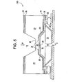
- the absolute pressure sensor 100 includes a base substrate 12, a cap substrate 14, and a chamber 16 disposed therebetween.
- the base substrate 12 and the cap substrate 14 each include silicon.
- the base substrate 12 and the cap substrate 14 each are a multi-layer structure (e.g., a silicon-on-insulator type wafer).
- the base substrate 12 and the cap substrate 14 are each a single-layer structure. It is advantageously noted that use of the single-layer structure can reduce the cost of the sensor compared to multi-layer structures.
- the base substrate 12 is an n-type substrate.
- the silicon of the base substrate 12 is doped with an n-type dopant (e.g., phosphorous).
- the cap substrate 14 can be either an n-type substrate or a p-type substrate.
- the cap substrate 14 can be doped with a similar or different n-type dopant as that employed in the base substrate 12.
- the cap substrate 14 is doped with a p-type dopant (e.g., boron).
- the base substrate 12 includes a cavity 18, which is defined by walls created in a support portion 20 of the base substrate 12 and defined on a third side by a diaphragm portion 22 of the base substrate 12. Stated another way, the diaphragm portion is disposed over the cavity 18. Further, the cavity 18 exposes a first (environmental) side 24 of the diaphragm portion 22 to an environment to be sensed. For example, during operation the environment exerts a pressure, illustrated as line P, against the first side 24 of the diaphragm portion 22.
- the diaphragm portion 22 includes a thickness sufficient to allow the diaphragm to deflect under pressure from the environment. Piezo-resistive elements 26 are disposed on a second surface 28 of the diaphragm portion 22.
- the piezo-resistive elements 26 are disposed in a region of the diaphragm portion 22 that has the greatest stress during flexure of the diaphragm portion 22.
- the piezo-resistive elements 26 each include a resistance that varies with mechanical stress. The number, type, and arrangement of each piezo-resistive element 26 vary depending on the application.
- the piezo-resistive elements 26 are arranged in a Wheatstone bridge circuit. During operation, the piezo-resistive elements 26 measure the flexion of the diaphragm portion 22 due the pressure form the environment. Suitable materials for the piezo-resistive element include, but are not limited, to p-type dopants (e.g., boron).
- the conductive pathway 30 includes any electrical conductive material.
- the conductive pathway 30 can include a portion of the base substrate 12, which has been doped with a p-type dopant.
- the conductive pathway 30 is disposed in electrical communication with an electrode 32, which is sometimes referred to as a wire bond pad, and the like.
- Suitable materials for the electrode 32 include metals (e.g., aluminum, titanium, platinum, gold, and combinations comprising at least one of the foregoing), alloys, and the like.
- the conductive pathway 30 is disposed in physical communication with the base portion 12.
- a first oxide layer 34 e.g., a silicon dioxide layer
- the first oxide layer 34 can be disposed on the conductive pathway 30 and at least a portion of the base substrate 12 (e.g., the second side of the diaphragm portion 22). Through holes are disposed in the first oxide layer 34 to allow electrical communication between the electrode 32 and the conductive pathway 30.
- first nitride layer 36 Disposed in physical communication with the first oxide layer 34 is first nitride layer 36. Through holes are disposed in the first nitride layer 36 corresponding to the location of the through holes disposed in the first oxide layer 34 to allow electrical communication between the electrode 32 and the conductive pathway 30. Without wanting be bound by theory, the first oxide layer 34 and the first nitride layer 36 each act as insulating layers and/or protective layers for the conductive pathway 30 and the piezo-resistive element 26.
- the first nitride layer 36 includes nitrides, including, but not limited to, silicon nitride.
- a second oxide layer 38 and a second nitride layer 40 are respectively disposed on a surface 42 of the base substrate 12, which is opposite, for example, the second side 28 of the diaphragm portion 22. These layers respectively include similar materials to those discussed in relation to first oxide layer 24 and first nitride layer 36. Further, the second oxide layer 38 and second nitride layer 40 each act as a protective coating during formation of cavity 18.
- the base substrate 12 is silicon fusion bonded to the cap substrate 14 such that a chamber 16 is formed therebetween, which is hermetically sealed from a surrounding environment.
- MIL-STD United States military standard
- the base substrate 12 and the cap substrate 14 are bonded together in a vacuum such that chamber 16 is a vacuum chamber, which functions as a zero pressure reference when the diaphragm portion 22 is exposed to the environment.
- the chamber 18 is formed by a cavity in the cap substrate 14.
- a cavity can be disposed in the base substrate 12 to form the chamber 16.
- the length and width of the cavity forming chamber 16 is selected to correspond to at least a length and width of the diaphragm portion 22.
- the width of the cavity can be substantially uniform (e.g., the walls are substantially straight) or the walls of the cavity can converge toward the diaphragm portion 22 (e.g. the walls are tapered).
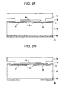
- FIGs 2(a)-2(j) collectively illustrate an exemplary method of making the embodiment of the backside absolute pressure sensor in Figure 1 .
- the piezo-resistive element 26 and the conductive pathway 30 are formed on a surface of the base substrate 12 by, for example, ion implantation, diffusion, and the like. Materials for the piezo-resistive element 26 and conductive pathway 30 include those materials discussed above.
- Figure 2(b) illustrates the selective etching away of a portion of the nitride layer 36 to form a bond area (e.g., a bond ring), which is followed by reoxidizing of the base substrate 12 to generate a thicker oxide portion of the first oxidizing layer in the bond area relative to the thickness of the first oxidizing layer 34 prior to etching and oxidizing.
- Figure 2(c) illustrates the etching away a portion of the nitride layer 36, while leaving the oxide layer 34, at a location corresponding to the location of electrodes 32.
- Figure 2(d) illustrates the cap substrate 14 including two step heights, which are formed on the cap substrate 14 by, for example, deep reactive ion etching. The step heights correspond to the desired size of the chamber 16 and are located to correspond to the bond area on the base substrate 12.
- Figure 2(e) illustrates the base substrate 12 being silicon fusion bonded to the cap substrate 14, which is an important feature in making the absolute pressure sensor 100.
- the base substrate 12 and the cap substrate 14 are bonded without any intermediate bond, alloy, adhesive, and the like.
- silicon fusion bonding refers to the bonding of silicon to silicon or any combination of bonding silicon to a silicon oxide.
- the silicon fusion bonding has a bond width of about 100 micrometers to about 150 micrometers. The use of silicon fusion bonding allows the pressure sensor 100 to have an active life of at least 10 years, which advantageously allows the absolute pressure sensor 100 to be employed in automotive applications.
- the overall cost of the absolute pressure sensor can be reduced compared to other devices that employ other bonding technologies.
- a silicon substrate which is bonded to another silicon substrate using an intermediate layer, has the additional costs associated with the bond material and added processing costs compared to silicon fusion bonding.
- the cost of glass substrates and silicon-on-insulator (SOI) substrates are generally more expensive than the cost of standard silicon substrates. In a competitive market, any reduction in cost, while maintaining or increasing performance, is desirable in gaining market share.
- Figure 2(f) illustrates the cap substrate 14 being thinned down using grinding and polishing to reduce the overall thickness of the cap substrate 14.
- the overall thickness of cap substrate 14 is up to about 400 micrometers, particularly about 50 micrometers to about 150 micrometers.
- a reduction in material corresponds to a reduction in the overall cost of the device.
- a reduction in size in a pressure sensor allows the pressure sensor to be employed in a wider range of applications.
- Figure 2(g) illustrates a window being formed into the second oxide layer 38 and the second nitride layer 40 by selectively removing a portion of each layer using an etchant similar to the etchant discussed above in relation to the selective removal of first oxide layer 36.
- the cap layer is formed into a final shape, by for example etching.
- Figure 2(i) illustrates electrodes 32 being formed by metallization in the area where a window (e.g., a through hole) is formed in each of the first oxide layer 34 and first nitride layer 26. Suitable metallization techniques include, but are not limited to, sputtering and electron beam evaporation deposition.
- Figure 2(j) illustrates the window formed in the second oxide layer 38 and the second nitride layer 40 being further opened (deepened) by for example, by etching, to form the cavity 18 and the diaphragm portion 22.
- the cavity 18 is formed using an anisotropic etchant.
- Suitable anisotropic etchants include, but are not limited to, potassium hydroxide (KOH), tetramethyl ammonium hydroxide (TMAH), ethylene diamine pyrocatechol (EDP), and the like.
- KOH potassium hydroxide
- TMAH tetramethyl ammonium hydroxide
- EDP ethylene diamine pyrocatechol
- the anisotropic etching forms the cavity 18 in the base substrate 12 having walls which generally converge from the surface 42 toward the first side 24 of the diaphragm portion 22 formed by the cavity 18.
- isotropic etching can be used to form the cavity 18.
- Suitable isotropic etchants include those known in the art, as well
- an embodiment of an absolute pressure sensor is illustrated. While the arrangement of the components of the absolute pressure sensor 200 are substantially the same as the arrangement illustrated by absolute pressure sensor 100, this embodiment is included herein to highlight that the shape of the chamber 16 and the shape of each substrate (e.g., cap substrate 14) can vary. Further, while the chamber 16 is disposed between the base substrate 12 and the cap substrate 14, the chamber 16 can be formed by a cavity in the base substrate 12, a cavity in the cap substrate 14, or a combination of the foregoing. In this example, the shape of the chamber 16 corresponds to the shape of the cap substrate 14.
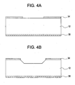
- Figures 4(a)-4(h) collectively illustrate an exemplary method of making the embodiment of the backside absolute pressure sensor illustrated in Figure 3 .
- Figure 4(a) illustrates a window being opened into the first oxide layer 34, which is further etched as illustrated in Figure 4(b) .
- an anisotropic etchant e.g., KOH, TMAH, EDP, and the like
- KOH, TMAH, EDP, and the like can be used to form a cavity in the base substrate 12 having tapered walls.
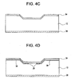
- An oxide is regrown in the etched area as illustrated in Figure 4(c) .
- the piezo-resistive element 26 and the conductive pathway 30 are formed on a surface of the base substrate 12 by ion implantation, diffusion, and the like.
- FIG. 4(e) illustrates the base substrate 12 being silicon fusion bonded to the cap substrate 14.
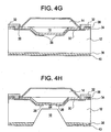
- Figure 4(f) illustrates a silicon nitride being disposed over the first oxide layer 34 and over an outer surface of the cap substrate 14.
- Figure 4(g) illustrates electrodes 32 being formed by metallization such that the electrodes electrically communicate with the conductive pathway 30. Suitable metallization techniques include those metallization techniques discussed above.
- Figure 4(h) illustrates the second oxide layer 38 and the second nitride layer 40 being etched to form cavity 18 and diaphragm portion 22.
- the differential pressure sensor 300 includes a similar arrangement of components discussed in relation to absolute pressure sensors 100 and 200, with the exception that the differential pressure 300 further includes a cavity 44 disposed through the cap substrate 14.
- the cavity 44 exposes the chamber 16 to the environment, which allows pressure to act on the diaphragm portion 22 from both the first side 24 and the second side 28. More particularly, in operation, the diaphragm portion 22 flexes in proportion to the difference in pressure from P and P 2 .
- the piezo-resistive elements 26 measure the flexion of the diaphragm portion 22 due that difference in pressure from P and P 2 .
- the absolute pressure sensors 100 and 200 can each be made into a differential pressure sensor 300 by etching the cavity 44 into the cap substrate 14. Suitable etchants include, but are not limited to, KOH and TMAH.
- the resulting differential pressure sensor 300 can be fixed to a ceramic substrate by solder bumping and the like.
- a solder bump (shown as an elliptical shape) is disposed in physical communication with electrode 32 and a second electrode, which is disposed on a ceramic substrate.
- the method of forming the differential pressure sensor 300 advantageously mitigates debris and the like from being disposed in the cavity 44, which can potentially build up and block the cavity 44.
- the absolute pressure sensors disclosed herein include a silicon fusion bond between a base substrate and a cap substrate. Further, the absolute pressure sensors are backside absolute pressure sensors.
- the silicon fusion bond provides a bond strength superior to other bonding techniques (e.g., an intermediate glass frit bond, an adhesive bond, and the like), which allows the pressure sensor to have a useful life of at least 10 years. Further, as briefly mentioned above, silicon fusion bonding also allows the pressure sensor to be constructed at a reduced cost compared to some present day sensors, which can offer a significant commercial advantage. Additionally, by constructing the absolute pressure sensors as a backside pressure sensors, the pressure sensors can advantageously be employed in harsh environments, since the piezo-resistive elements and conductive pathways are shielded from the environment. Again, this construction can increase the useful life of the pressure sensor compared to present day sensors.
Landscapes
- Physics & Mathematics (AREA)
- General Physics & Mathematics (AREA)
- Engineering & Computer Science (AREA)
- Microelectronics & Electronic Packaging (AREA)
- Chemical & Material Sciences (AREA)
- Analytical Chemistry (AREA)
- Measuring Fluid Pressure (AREA)
- Pressure Sensors (AREA)
Applications Claiming Priority (2)
| Application Number | Priority Date | Filing Date | Title |
|---|---|---|---|
| US11/210,309 US7622782B2 (en) | 2005-08-24 | 2005-08-24 | Pressure sensors and methods of making the same |
| PCT/US2006/032858 WO2007024911A2 (en) | 2005-08-24 | 2006-08-22 | Pressure sensors and methods of making the same |
Publications (2)
| Publication Number | Publication Date |
|---|---|
| EP1920229A2 EP1920229A2 (en) | 2008-05-14 |
| EP1920229B1 true EP1920229B1 (en) | 2011-11-02 |
Family
ID=37487427
Family Applications (1)
| Application Number | Title | Priority Date | Filing Date |
|---|---|---|---|
| EP06802137A Not-in-force EP1920229B1 (en) | 2005-08-24 | 2006-08-22 | Pressure sensors and methods of making the same |
Country Status (7)
| Country | Link |
|---|---|
| US (1) | US7622782B2 (enExample) |
| EP (1) | EP1920229B1 (enExample) |
| JP (1) | JP5342236B2 (enExample) |
| KR (1) | KR101296031B1 (enExample) |
| CN (1) | CN101248340B (enExample) |
| AT (1) | ATE532044T1 (enExample) |
| WO (1) | WO2007024911A2 (enExample) |
Families Citing this family (80)
| Publication number | Priority date | Publication date | Assignee | Title |
|---|---|---|---|---|
| US7304412B2 (en) * | 2005-01-31 | 2007-12-04 | Avago Technologes Wireless Ip (Singapore) Pte Ltd | Apparatus embodying doped substrate portion |
| TWI289879B (en) * | 2005-09-30 | 2007-11-11 | Touch Micro System Tech | Method of fabricating pressure sensor |
| US7880113B2 (en) * | 2005-12-01 | 2011-02-01 | Delphi Technologies, Inc. | Plasma discharge method and structure for verifying a hermetical seal |
| FR2897937B1 (fr) * | 2006-02-24 | 2008-05-23 | Commissariat Energie Atomique | Capteur de pression a jauges resistives |
| DE102007027274A1 (de) * | 2007-06-11 | 2008-12-18 | Endress + Hauser Gmbh + Co. Kg | Differenzdrucksensor |
| US7784330B2 (en) * | 2007-10-05 | 2010-08-31 | Schlumberger Technology Corporation | Viscosity measurement |
| TWI364804B (en) * | 2007-11-14 | 2012-05-21 | Ind Tech Res Inst | Wafer level sensor package structure and method therefor |
| JP5001129B2 (ja) * | 2007-12-17 | 2012-08-15 | ホーチキ株式会社 | 熱センサ |
| US8297125B2 (en) | 2008-05-23 | 2012-10-30 | Honeywell International Inc. | Media isolated differential pressure sensor with cap |
| US8230745B2 (en) | 2008-11-19 | 2012-07-31 | Honeywell International Inc. | Wet/wet differential pressure sensor based on microelectronic packaging process |
| DE102008054415A1 (de) | 2008-12-09 | 2010-06-10 | Robert Bosch Gmbh | Anordnung zweier Substrate mit einer SLID-Bondverbindung und Verfahren zur Herstellung einer solchen Anordnung |
| US7900521B2 (en) * | 2009-02-10 | 2011-03-08 | Freescale Semiconductor, Inc. | Exposed pad backside pressure sensor package |
| US8471346B2 (en) * | 2009-02-27 | 2013-06-25 | Infineon Technologies Ag | Semiconductor device including a cavity |
| US8237235B2 (en) * | 2009-04-14 | 2012-08-07 | Taiwan Semiconductor Manufacturing Company, Ltd. | Metal-ceramic multilayer structure |
| US8322225B2 (en) * | 2009-07-10 | 2012-12-04 | Honeywell International Inc. | Sensor package assembly having an unconstrained sense die |
| TWI388038B (zh) * | 2009-07-23 | 2013-03-01 | Ind Tech Res Inst | 感測元件結構與製造方法 |
| US8739626B2 (en) | 2009-08-04 | 2014-06-03 | Fairchild Semiconductor Corporation | Micromachined inertial sensor devices |
| US8258745B2 (en) | 2009-09-10 | 2012-09-04 | Syntheon, Llc | Surgical sterilizer with integrated battery charging device |
| US8082797B2 (en) | 2009-11-11 | 2011-12-27 | Honeywell International Inc. | Pressure sensor assembly |
| US8421168B2 (en) * | 2009-11-17 | 2013-04-16 | Fairchild Semiconductor Corporation | Microelectromechanical systems microphone packaging systems |
| JP5771900B2 (ja) * | 2010-03-26 | 2015-09-02 | セイコーエプソン株式会社 | 熱型光検出器、熱型光検出装置及び電子機器 |
| US8435821B2 (en) * | 2010-06-18 | 2013-05-07 | General Electric Company | Sensor and method for fabricating the same |
| US8230743B2 (en) | 2010-08-23 | 2012-07-31 | Honeywell International Inc. | Pressure sensor |
| WO2012037492A2 (en) | 2010-09-18 | 2012-03-22 | Janusz Bryzek | Multi-die mems package |
| US9278845B2 (en) | 2010-09-18 | 2016-03-08 | Fairchild Semiconductor Corporation | MEMS multi-axis gyroscope Z-axis electrode structure |
| EP2616771B8 (en) | 2010-09-18 | 2018-12-19 | Fairchild Semiconductor Corporation | Micromachined monolithic 6-axis inertial sensor |
| CN103221331B (zh) | 2010-09-18 | 2016-02-03 | 快捷半导体公司 | 用于微机电系统的密封封装 |
| DE112011103124B4 (de) | 2010-09-18 | 2025-10-30 | Fairchild Semiconductor Corporation | Biegelager zum Verringern von Quadratur für mitschwingende mikromechanische Vorrichtungen |
| US9455354B2 (en) | 2010-09-18 | 2016-09-27 | Fairchild Semiconductor Corporation | Micromachined 3-axis accelerometer with a single proof-mass |
| EP2619130A4 (en) | 2010-09-20 | 2014-12-10 | Fairchild Semiconductor | SILICONE CONTINUITY WITH REDUCED CROSS-CAPACITY |
| EP2619536B1 (en) | 2010-09-20 | 2016-11-02 | Fairchild Semiconductor Corporation | Microelectromechanical pressure sensor including reference capacitor |
| DE102010063065A1 (de) * | 2010-12-14 | 2012-06-14 | Endress + Hauser Gmbh + Co. Kg | Drucksensor und Verfahren zu dessen Herstellung+ |
| US8809975B2 (en) * | 2010-12-15 | 2014-08-19 | Panasonic Corporation | Semiconductor pressure sensor |
| US7998777B1 (en) | 2010-12-15 | 2011-08-16 | General Electric Company | Method for fabricating a sensor |
| CN102183335B (zh) | 2011-03-15 | 2015-10-21 | 迈尔森电子(天津)有限公司 | Mems压力传感器及其制作方法 |
| US8709848B2 (en) * | 2011-04-15 | 2014-04-29 | Freescale Semiconductor, Inc. | Method for etched cavity devices |
| US8993451B2 (en) * | 2011-04-15 | 2015-03-31 | Freescale Semiconductor, Inc. | Etching trenches in a substrate |
| US8466523B2 (en) * | 2011-10-07 | 2013-06-18 | Continental Automotive Systems, Inc. | Differential pressure sensor device |
| US9062972B2 (en) | 2012-01-31 | 2015-06-23 | Fairchild Semiconductor Corporation | MEMS multi-axis accelerometer electrode structure |
| US8978475B2 (en) | 2012-02-01 | 2015-03-17 | Fairchild Semiconductor Corporation | MEMS proof mass with split z-axis portions |
| US9170164B2 (en) | 2012-02-03 | 2015-10-27 | Dieter Naegele-Preissmann | Capacitive pressure sensor and a method of fabricating the same |
| US8754694B2 (en) | 2012-04-03 | 2014-06-17 | Fairchild Semiconductor Corporation | Accurate ninety-degree phase shifter |
| US8742964B2 (en) | 2012-04-04 | 2014-06-03 | Fairchild Semiconductor Corporation | Noise reduction method with chopping for a merged MEMS accelerometer sensor |
| US9488693B2 (en) | 2012-04-04 | 2016-11-08 | Fairchild Semiconductor Corporation | Self test of MEMS accelerometer with ASICS integrated capacitors |
| US9069006B2 (en) | 2012-04-05 | 2015-06-30 | Fairchild Semiconductor Corporation | Self test of MEMS gyroscope with ASICs integrated capacitors |
| EP2647952B1 (en) | 2012-04-05 | 2017-11-15 | Fairchild Semiconductor Corporation | Mems device automatic-gain control loop for mechanical amplitude drive |
| EP2648334B1 (en) | 2012-04-05 | 2020-06-10 | Fairchild Semiconductor Corporation | Mems device front-end charge amplifier |
| EP2647955B8 (en) | 2012-04-05 | 2018-12-19 | Fairchild Semiconductor Corporation | MEMS device quadrature phase shift cancellation |
| US9625272B2 (en) | 2012-04-12 | 2017-04-18 | Fairchild Semiconductor Corporation | MEMS quadrature cancellation and signal demodulation |
| US9094027B2 (en) | 2012-04-12 | 2015-07-28 | Fairchild Semiconductor Corporation | Micro-electro-mechanical-system (MEMS) driver |
| US8833172B2 (en) * | 2012-06-27 | 2014-09-16 | Continental Automotive Systems, Inc | Pressure sensing device with stepped cavity to minimize thermal noise |
| US9010200B2 (en) | 2012-08-06 | 2015-04-21 | Amphenol Thermometrics, Inc. | Device for measuring forces and method of making the same |
| DE102013014881B4 (de) | 2012-09-12 | 2023-05-04 | Fairchild Semiconductor Corporation | Verbesserte Silizium-Durchkontaktierung mit einer Füllung aus mehreren Materialien |
| CN104736983B (zh) * | 2012-10-17 | 2017-05-31 | 株式会社鹭宫制作所 | 压力传感器以及具备该压力传感器的传感器单元 |
| GB2508908B (en) | 2012-12-14 | 2017-02-15 | Gen Electric | Resonator device |
| CN103964370A (zh) * | 2013-01-29 | 2014-08-06 | 北京大学 | 一种电容式压力传感器的制备方法 |
| US8878316B2 (en) * | 2013-02-22 | 2014-11-04 | Continental Automotive Systems, Inc. | Cap side bonding structure for backside absolute pressure sensors |
| JP2014169915A (ja) * | 2013-03-04 | 2014-09-18 | Denso Corp | 半導体圧力センサの製造方法 |
| JP5783297B2 (ja) * | 2013-08-06 | 2015-09-24 | 株式会社デンソー | 力学量センサ |
| US9546922B2 (en) * | 2013-08-09 | 2017-01-17 | Continental Automotive Systems, Inc. | Absolute pressure sensor with improved cap bonding boundary |
| CN103674397B (zh) * | 2013-12-03 | 2016-04-20 | 新会康宇测控仪器仪表工程有限公司 | 高过载背压式绝压传感器模块及其制造工艺 |
| US9260294B2 (en) * | 2013-12-27 | 2016-02-16 | Intel Corporation | Integration of pressure or inertial sensors into integrated circuit fabrication and packaging |
| US11402288B2 (en) * | 2014-04-04 | 2022-08-02 | Robert Bosch Gmbh | Membrane-based sensor having a plurality of spacers extending from a cap layer |
| US20160178467A1 (en) * | 2014-07-29 | 2016-06-23 | Silicon Microstructures, Inc. | Pressure sensor having cap-defined membrane |
| JP2017509860A (ja) * | 2014-07-29 | 2017-04-06 | シリコン マイクロストラクチャーズ, インコーポレイテッドSilicon Microstructures, Inc. | キャップで規定されたメンブレン(cap−defined membrane)を有する圧力センサ |
| CN104296899B (zh) * | 2014-09-28 | 2017-04-12 | 缪建民 | 高灵敏度硅压阻压力传感器及其制备方法 |
| CN105527042B (zh) * | 2014-10-15 | 2020-06-05 | 浙江盾安人工环境股份有限公司 | 压力传感器及其制造方法 |
| US9939338B2 (en) * | 2015-02-19 | 2018-04-10 | Stmicroelectronics S.R.L. | Pressure sensing device with cavity and related methods |
| CN205262665U (zh) | 2015-06-22 | 2016-05-25 | 意法半导体股份有限公司 | 压力传感器 |
| CN105241369B (zh) * | 2015-08-17 | 2018-02-09 | 王文 | 一种mems应变计芯片及其制造工艺 |
| JP6555214B2 (ja) * | 2016-08-25 | 2019-08-07 | 株式会社デンソー | 圧力センサ |
| US10481025B2 (en) | 2017-01-26 | 2019-11-19 | Rosemount Aerospace Inc. | Piezoresistive sensor with spring flexures for stress isolation |
| JP6468304B2 (ja) * | 2017-02-28 | 2019-02-13 | 株式会社デンソー | 物理量センサ |
| KR101985946B1 (ko) * | 2018-11-21 | 2019-06-04 | 호산엔지니어링(주) | Msg를 이용한 로드셀 장치 |
| CN109682510B (zh) * | 2018-12-07 | 2021-05-04 | 中国电子科技集团公司第十三研究所 | GaN高温压力传感器 |
| CN109668661B (zh) * | 2018-12-07 | 2021-05-04 | 中国电子科技集团公司第十三研究所 | GaN高温压力传感器 |
| CN111337166A (zh) * | 2020-03-25 | 2020-06-26 | 电子科技大学 | 一种新型绝对压声表面波压力传感器的制备方法 |
| MX2024002230A (es) * | 2021-08-31 | 2024-03-05 | Huba Control Ag | Celda de medicion de la presion metalica. |
| CN114577390A (zh) * | 2022-03-03 | 2022-06-03 | 苏州跃芯微传感技术有限公司 | 一种低压mems压力传感器及其制备方法 |
| CN118168706A (zh) * | 2024-03-13 | 2024-06-11 | 京东方科技集团股份有限公司 | 压力传感器、压力传感器的制造方法、空调装置与车辆 |
Family Cites Families (30)
| Publication number | Priority date | Publication date | Assignee | Title |
|---|---|---|---|---|
| JPS5544786A (en) | 1978-09-27 | 1980-03-29 | Hitachi Ltd | Pressure sensor |
| US4525766A (en) | 1984-01-25 | 1985-06-25 | Transensory Devices, Inc. | Method and apparatus for forming hermetically sealed electrical feedthrough conductors |
| US4800758A (en) * | 1986-06-23 | 1989-01-31 | Rosemount Inc. | Pressure transducer with stress isolation for hard mounting |
| JPH0810170B2 (ja) | 1987-03-06 | 1996-01-31 | 株式会社日立製作所 | 半導体絶対圧力センサの製造方法 |
| US5095349A (en) * | 1988-06-08 | 1992-03-10 | Nippondenso Co., Ltd. | Semiconductor pressure sensor and method of manufacturing same |
| US5157973A (en) | 1989-03-16 | 1992-10-27 | Process Automation Business, Inc. | Pressure sensor with integral overpressure protection |
| US5231301A (en) | 1991-10-02 | 1993-07-27 | Lucas Novasensor | Semiconductor sensor with piezoresistors and improved electrostatic structures |
| KR940010493B1 (ko) | 1991-11-21 | 1994-10-24 | 한국과학기술연구원 | 실리콘기판의 용융접합방법 및 장치 |
| JPH07110277A (ja) * | 1993-10-08 | 1995-04-25 | Oki Electric Ind Co Ltd | シリコン圧力センサ |
| US5591679A (en) | 1995-04-12 | 1997-01-07 | Sensonor A/S | Sealed cavity arrangement method |
| JP3401992B2 (ja) * | 1995-05-17 | 2003-04-28 | 株式会社デンソー | 半導体感歪センサ |
| US5600071A (en) | 1995-09-05 | 1997-02-04 | Motorola, Inc. | Vertically integrated sensor structure and method |
| US6472244B1 (en) | 1996-07-31 | 2002-10-29 | Sgs-Thomson Microelectronics S.R.L. | Manufacturing method and integrated microstructures of semiconductor material and integrated piezoresistive pressure sensor having a diaphragm of polycrystalline semiconductor material |
| WO1998015807A1 (en) | 1996-10-07 | 1998-04-16 | Lucas Novasensor | Silicon at least 5 micron high acute cavity with channel by oxidizing fusion bonding and stop etching |
| JPH10325772A (ja) * | 1997-05-27 | 1998-12-08 | Nissan Motor Co Ltd | 半導体圧力センサおよびその製造方法 |
| DE69922727T2 (de) * | 1998-03-31 | 2005-12-15 | Hitachi, Ltd. | Kapazitiver Druckwandler |
| JPH11311579A (ja) * | 1998-04-28 | 1999-11-09 | Matsushita Electric Works Ltd | 半導体圧力センサのダイアフラム形成方法 |
| US6074891A (en) | 1998-06-16 | 2000-06-13 | Delphi Technologies, Inc. | Process for verifying a hermetic seal and semiconductor device therefor |
| EP1093571B1 (en) | 1998-07-07 | 2003-05-21 | The Goodyear Tire & Rubber Company | Method of fabricating silicon capacitive sensor |
| JP3545224B2 (ja) * | 1998-10-06 | 2004-07-21 | 株式会社日立ユニシアオートモティブ | 圧力センサ |
| US6406636B1 (en) | 1999-06-02 | 2002-06-18 | Megasense, Inc. | Methods for wafer to wafer bonding using microstructures |
| JP2002039892A (ja) * | 2000-07-28 | 2002-02-06 | Matsushita Electric Works Ltd | 半導体圧力センサとその製造方法 |
| US7381630B2 (en) | 2001-01-02 | 2008-06-03 | The Charles Stark Draper Laboratory, Inc. | Method for integrating MEMS device and interposer |
| EP1359402B1 (en) | 2002-05-01 | 2014-10-01 | Infineon Technologies AG | Pressure sensor |
| US6647794B1 (en) * | 2002-05-06 | 2003-11-18 | Rosemount Inc. | Absolute pressure sensor |
| DE10257097B4 (de) | 2002-12-05 | 2005-12-22 | X-Fab Semiconductor Foundries Ag | Verfahren zur Herstellung von mikroelektromechanischen Systemen (Microelectromechanical Systems: MEMS) mittels Silizium-Hochtemperatur-Fusionsbonden |
| JP2005043159A (ja) * | 2003-07-25 | 2005-02-17 | Hitachi Unisia Automotive Ltd | 圧力センサ |
| EP1522521B1 (en) | 2003-10-10 | 2015-12-09 | Infineon Technologies AG | Capacitive sensor |
| JP4314977B2 (ja) * | 2003-11-20 | 2009-08-19 | パナソニック電工株式会社 | 圧力センサ及び該圧力センサの製造方法 |
| JP2005221453A (ja) * | 2004-02-09 | 2005-08-18 | Denso Corp | 圧力センサ |
-
2005
- 2005-08-24 US US11/210,309 patent/US7622782B2/en not_active Expired - Fee Related
-
2006
- 2006-08-22 AT AT06802137T patent/ATE532044T1/de active
- 2006-08-22 CN CN2006800310976A patent/CN101248340B/zh not_active Expired - Fee Related
- 2006-08-22 JP JP2008528091A patent/JP5342236B2/ja not_active Expired - Fee Related
- 2006-08-22 WO PCT/US2006/032858 patent/WO2007024911A2/en not_active Ceased
- 2006-08-22 EP EP06802137A patent/EP1920229B1/en not_active Not-in-force
- 2006-08-22 KR KR1020087004343A patent/KR101296031B1/ko not_active Expired - Fee Related
Also Published As
| Publication number | Publication date |
|---|---|
| KR20080031969A (ko) | 2008-04-11 |
| CN101248340A (zh) | 2008-08-20 |
| EP1920229A2 (en) | 2008-05-14 |
| KR101296031B1 (ko) | 2013-08-12 |
| US20070052046A1 (en) | 2007-03-08 |
| CN101248340B (zh) | 2012-11-14 |
| US7622782B2 (en) | 2009-11-24 |
| ATE532044T1 (de) | 2011-11-15 |
| WO2007024911A2 (en) | 2007-03-01 |
| JP2009506323A (ja) | 2009-02-12 |
| WO2007024911A3 (en) | 2007-06-14 |
| JP5342236B2 (ja) | 2013-11-13 |
Similar Documents
| Publication | Publication Date | Title |
|---|---|---|
| EP1920229B1 (en) | Pressure sensors and methods of making the same | |
| US5295395A (en) | Diaphragm-based-sensors | |
| US7998777B1 (en) | Method for fabricating a sensor | |
| EP2339357B1 (en) | Method for fabricating a sensor | |
| TWI685464B (zh) | 壓力感測器及其製造方法 | |
| US6109113A (en) | Silicon micromachined capacitive pressure sensor and method of manufacture | |
| KR102161035B1 (ko) | 센서 디바이스 및 그 제조 방법 | |
| US8230746B2 (en) | Combined type pressure gauge, and manufacturing method of combined type pressure gauge | |
| EP3052901B1 (en) | Inertial and pressure sensors on single chip | |
| WO2010049794A1 (en) | Pressure sensor and wire guide assembly | |
| JP2015515609A (ja) | カテーテルダイおよびその製造方法 | |
| JP6122880B2 (ja) | 圧力センサ及び対応するセンサの製造方法 | |
| US6794271B2 (en) | Method for fabricating a microelectromechanical system (MEMS) device using a pre-patterned bridge | |
| EP2182340A1 (en) | Pressure Sensor and Guide Wire Assembly | |
| US7478562B2 (en) | High temperature LC pressure transducer and methods for making the same | |
| JP3173256B2 (ja) | 半導体加速度センサとその製造方法 | |
| EP2873095B1 (en) | Semiconductor secured to substrate via hole in substrate | |
| JP2003004566A (ja) | 静電容量型圧力センサ及びその製造方法 |
Legal Events
| Date | Code | Title | Description |
|---|---|---|---|
| PUAI | Public reference made under article 153(3) epc to a published international application that has entered the european phase |
Free format text: ORIGINAL CODE: 0009012 |
|
| 17P | Request for examination filed |
Effective date: 20080325 |
|
| AK | Designated contracting states |
Kind code of ref document: A2 Designated state(s): AT BE BG CH CY CZ DE DK EE ES FI FR GB GR HU IE IS IT LI LT LU LV MC NL PL PT RO SE SI SK TR |
|
| 17Q | First examination report despatched |
Effective date: 20080701 |
|
| GRAP | Despatch of communication of intention to grant a patent |
Free format text: ORIGINAL CODE: EPIDOSNIGR1 |
|
| DAX | Request for extension of the european patent (deleted) | ||
| GRAS | Grant fee paid |
Free format text: ORIGINAL CODE: EPIDOSNIGR3 |
|
| GRAA | (expected) grant |
Free format text: ORIGINAL CODE: 0009210 |
|
| AK | Designated contracting states |
Kind code of ref document: B1 Designated state(s): AT BE BG CH CY CZ DE DK EE ES FI FR GB GR HU IE IS IT LI LT LU LV MC NL PL PT RO SE SI SK TR |
|
| REG | Reference to a national code |
Ref country code: GB Ref legal event code: FG4D |
|
| REG | Reference to a national code |
Ref country code: CH Ref legal event code: EP |
|
| REG | Reference to a national code |
Ref country code: IE Ref legal event code: FG4D |
|
| REG | Reference to a national code |
Ref country code: DE Ref legal event code: R096 Ref document number: 602006025601 Country of ref document: DE Effective date: 20111229 |
|
| REG | Reference to a national code |
Ref country code: NL Ref legal event code: VDEP Effective date: 20111102 |
|
| LTIE | Lt: invalidation of european patent or patent extension |
Effective date: 20111102 |
|
| PG25 | Lapsed in a contracting state [announced via postgrant information from national office to epo] |
Ref country code: LT Free format text: LAPSE BECAUSE OF FAILURE TO SUBMIT A TRANSLATION OF THE DESCRIPTION OR TO PAY THE FEE WITHIN THE PRESCRIBED TIME-LIMIT Effective date: 20111102 Ref country code: IS Free format text: LAPSE BECAUSE OF FAILURE TO SUBMIT A TRANSLATION OF THE DESCRIPTION OR TO PAY THE FEE WITHIN THE PRESCRIBED TIME-LIMIT Effective date: 20120302 |
|
| PG25 | Lapsed in a contracting state [announced via postgrant information from national office to epo] |
Ref country code: PT Free format text: LAPSE BECAUSE OF FAILURE TO SUBMIT A TRANSLATION OF THE DESCRIPTION OR TO PAY THE FEE WITHIN THE PRESCRIBED TIME-LIMIT Effective date: 20120302 Ref country code: SI Free format text: LAPSE BECAUSE OF FAILURE TO SUBMIT A TRANSLATION OF THE DESCRIPTION OR TO PAY THE FEE WITHIN THE PRESCRIBED TIME-LIMIT Effective date: 20111102 Ref country code: LV Free format text: LAPSE BECAUSE OF FAILURE TO SUBMIT A TRANSLATION OF THE DESCRIPTION OR TO PAY THE FEE WITHIN THE PRESCRIBED TIME-LIMIT Effective date: 20111102 Ref country code: PL Free format text: LAPSE BECAUSE OF FAILURE TO SUBMIT A TRANSLATION OF THE DESCRIPTION OR TO PAY THE FEE WITHIN THE PRESCRIBED TIME-LIMIT Effective date: 20111102 Ref country code: GR Free format text: LAPSE BECAUSE OF FAILURE TO SUBMIT A TRANSLATION OF THE DESCRIPTION OR TO PAY THE FEE WITHIN THE PRESCRIBED TIME-LIMIT Effective date: 20120203 Ref country code: SE Free format text: LAPSE BECAUSE OF FAILURE TO SUBMIT A TRANSLATION OF THE DESCRIPTION OR TO PAY THE FEE WITHIN THE PRESCRIBED TIME-LIMIT Effective date: 20111102 Ref country code: NL Free format text: LAPSE BECAUSE OF FAILURE TO SUBMIT A TRANSLATION OF THE DESCRIPTION OR TO PAY THE FEE WITHIN THE PRESCRIBED TIME-LIMIT Effective date: 20111102 Ref country code: BE Free format text: LAPSE BECAUSE OF FAILURE TO SUBMIT A TRANSLATION OF THE DESCRIPTION OR TO PAY THE FEE WITHIN THE PRESCRIBED TIME-LIMIT Effective date: 20111102 |
|
| PG25 | Lapsed in a contracting state [announced via postgrant information from national office to epo] |
Ref country code: CY Free format text: LAPSE BECAUSE OF FAILURE TO SUBMIT A TRANSLATION OF THE DESCRIPTION OR TO PAY THE FEE WITHIN THE PRESCRIBED TIME-LIMIT Effective date: 20111102 |
|
| PG25 | Lapsed in a contracting state [announced via postgrant information from national office to epo] |
Ref country code: SK Free format text: LAPSE BECAUSE OF FAILURE TO SUBMIT A TRANSLATION OF THE DESCRIPTION OR TO PAY THE FEE WITHIN THE PRESCRIBED TIME-LIMIT Effective date: 20111102 Ref country code: EE Free format text: LAPSE BECAUSE OF FAILURE TO SUBMIT A TRANSLATION OF THE DESCRIPTION OR TO PAY THE FEE WITHIN THE PRESCRIBED TIME-LIMIT Effective date: 20111102 Ref country code: CZ Free format text: LAPSE BECAUSE OF FAILURE TO SUBMIT A TRANSLATION OF THE DESCRIPTION OR TO PAY THE FEE WITHIN THE PRESCRIBED TIME-LIMIT Effective date: 20111102 Ref country code: DK Free format text: LAPSE BECAUSE OF FAILURE TO SUBMIT A TRANSLATION OF THE DESCRIPTION OR TO PAY THE FEE WITHIN THE PRESCRIBED TIME-LIMIT Effective date: 20111102 Ref country code: BG Free format text: LAPSE BECAUSE OF FAILURE TO SUBMIT A TRANSLATION OF THE DESCRIPTION OR TO PAY THE FEE WITHIN THE PRESCRIBED TIME-LIMIT Effective date: 20120202 |
|
| PG25 | Lapsed in a contracting state [announced via postgrant information from national office to epo] |
Ref country code: RO Free format text: LAPSE BECAUSE OF FAILURE TO SUBMIT A TRANSLATION OF THE DESCRIPTION OR TO PAY THE FEE WITHIN THE PRESCRIBED TIME-LIMIT Effective date: 20111102 |
|
| PLBE | No opposition filed within time limit |
Free format text: ORIGINAL CODE: 0009261 |
|
| STAA | Information on the status of an ep patent application or granted ep patent |
Free format text: STATUS: NO OPPOSITION FILED WITHIN TIME LIMIT |
|
| 26N | No opposition filed |
Effective date: 20120803 |
|
| REG | Reference to a national code |
Ref country code: DE Ref legal event code: R097 Ref document number: 602006025601 Country of ref document: DE Effective date: 20120803 |
|
| REG | Reference to a national code |
Ref country code: CH Ref legal event code: PL |
|
| PG25 | Lapsed in a contracting state [announced via postgrant information from national office to epo] |
Ref country code: MC Free format text: LAPSE BECAUSE OF NON-PAYMENT OF DUE FEES Effective date: 20120831 |
|
| PG25 | Lapsed in a contracting state [announced via postgrant information from national office to epo] |
Ref country code: CH Free format text: LAPSE BECAUSE OF NON-PAYMENT OF DUE FEES Effective date: 20120831 Ref country code: LI Free format text: LAPSE BECAUSE OF NON-PAYMENT OF DUE FEES Effective date: 20120831 Ref country code: ES Free format text: LAPSE BECAUSE OF FAILURE TO SUBMIT A TRANSLATION OF THE DESCRIPTION OR TO PAY THE FEE WITHIN THE PRESCRIBED TIME-LIMIT Effective date: 20120213 |
|
| REG | Reference to a national code |
Ref country code: IE Ref legal event code: MM4A |
|
| PG25 | Lapsed in a contracting state [announced via postgrant information from national office to epo] |
Ref country code: IE Free format text: LAPSE BECAUSE OF NON-PAYMENT OF DUE FEES Effective date: 20120822 |
|
| PG25 | Lapsed in a contracting state [announced via postgrant information from national office to epo] |
Ref country code: TR Free format text: LAPSE BECAUSE OF FAILURE TO SUBMIT A TRANSLATION OF THE DESCRIPTION OR TO PAY THE FEE WITHIN THE PRESCRIBED TIME-LIMIT Effective date: 20111102 |
|
| PG25 | Lapsed in a contracting state [announced via postgrant information from national office to epo] |
Ref country code: LU Free format text: LAPSE BECAUSE OF NON-PAYMENT OF DUE FEES Effective date: 20120822 |
|
| PG25 | Lapsed in a contracting state [announced via postgrant information from national office to epo] |
Ref country code: HU Free format text: LAPSE BECAUSE OF FAILURE TO SUBMIT A TRANSLATION OF THE DESCRIPTION OR TO PAY THE FEE WITHIN THE PRESCRIBED TIME-LIMIT Effective date: 20060822 |
|
| PGFP | Annual fee paid to national office [announced via postgrant information from national office to epo] |
Ref country code: FI Payment date: 20141229 Year of fee payment: 9 Ref country code: GB Payment date: 20141230 Year of fee payment: 9 |
|
| PGFP | Annual fee paid to national office [announced via postgrant information from national office to epo] |
Ref country code: AT Payment date: 20141229 Year of fee payment: 9 Ref country code: FR Payment date: 20141226 Year of fee payment: 9 |
|
| PGFP | Annual fee paid to national office [announced via postgrant information from national office to epo] |
Ref country code: DE Payment date: 20141231 Year of fee payment: 9 Ref country code: IT Payment date: 20141231 Year of fee payment: 9 |
|
| REG | Reference to a national code |
Ref country code: DE Ref legal event code: R119 Ref document number: 602006025601 Country of ref document: DE |
|
| REG | Reference to a national code |
Ref country code: AT Ref legal event code: MM01 Ref document number: 532044 Country of ref document: AT Kind code of ref document: T Effective date: 20150822 |
|
| GBPC | Gb: european patent ceased through non-payment of renewal fee |
Effective date: 20150822 |
|
| PG25 | Lapsed in a contracting state [announced via postgrant information from national office to epo] |
Ref country code: IT Free format text: LAPSE BECAUSE OF NON-PAYMENT OF DUE FEES Effective date: 20150822 |
|
| PG25 | Lapsed in a contracting state [announced via postgrant information from national office to epo] |
Ref country code: AT Free format text: LAPSE BECAUSE OF NON-PAYMENT OF DUE FEES Effective date: 20150822 Ref country code: FI Free format text: LAPSE BECAUSE OF NON-PAYMENT OF DUE FEES Effective date: 20150822 |
|
| REG | Reference to a national code |
Ref country code: FR Ref legal event code: ST Effective date: 20160429 |
|
| PG25 | Lapsed in a contracting state [announced via postgrant information from national office to epo] |
Ref country code: GB Free format text: LAPSE BECAUSE OF NON-PAYMENT OF DUE FEES Effective date: 20150822 Ref country code: DE Free format text: LAPSE BECAUSE OF NON-PAYMENT OF DUE FEES Effective date: 20160301 |
|
| PG25 | Lapsed in a contracting state [announced via postgrant information from national office to epo] |
Ref country code: FR Free format text: LAPSE BECAUSE OF NON-PAYMENT OF DUE FEES Effective date: 20150831 |