EP1916705A2 - Halbleiterbauelement mit dotiertem Metall mit Hauptelektrode - Google Patents
Halbleiterbauelement mit dotiertem Metall mit Hauptelektrode Download PDFInfo
- Publication number
- EP1916705A2 EP1916705A2 EP07075906A EP07075906A EP1916705A2 EP 1916705 A2 EP1916705 A2 EP 1916705A2 EP 07075906 A EP07075906 A EP 07075906A EP 07075906 A EP07075906 A EP 07075906A EP 1916705 A2 EP1916705 A2 EP 1916705A2
- Authority
- EP
- European Patent Office
- Prior art keywords
- work function
- main electrode
- gate electrode
- layer
- gate
- Prior art date
- Legal status (The legal status is an assumption and is not a legal conclusion. Google has not performed a legal analysis and makes no representation as to the accuracy of the status listed.)
- Withdrawn
Links
Images






Classifications
-
- H—ELECTRICITY
- H10—SEMICONDUCTOR DEVICES; ELECTRIC SOLID-STATE DEVICES NOT OTHERWISE PROVIDED FOR
- H10D—INORGANIC ELECTRIC SEMICONDUCTOR DEVICES
- H10D64/00—Electrodes of devices having potential barriers
- H10D64/01—Manufacture or treatment
- H10D64/013—Manufacture or treatment of electrodes having a conductor capacitively coupled to a semiconductor by an insulator
- H10D64/01302—Manufacture or treatment of electrodes having a conductor capacitively coupled to a semiconductor by an insulator the insulator being formed after the semiconductor body, the semiconductor being silicon
- H10D64/01304—Manufacture or treatment of electrodes having a conductor capacitively coupled to a semiconductor by an insulator the insulator being formed after the semiconductor body, the semiconductor being silicon characterised by the conductor
- H10D64/01318—Manufacture or treatment of electrodes having a conductor capacitively coupled to a semiconductor by an insulator the insulator being formed after the semiconductor body, the semiconductor being silicon characterised by the conductor the conductor comprising a layer of alloy material, compound material or organic material contacting the insulator, e.g. TiN
- H10D64/0132—Manufacture or treatment of electrodes having a conductor capacitively coupled to a semiconductor by an insulator the insulator being formed after the semiconductor body, the semiconductor being silicon characterised by the conductor the conductor comprising a layer of alloy material, compound material or organic material contacting the insulator, e.g. TiN the conductor being a metallic silicide
-
- H—ELECTRICITY
- H10—SEMICONDUCTOR DEVICES; ELECTRIC SOLID-STATE DEVICES NOT OTHERWISE PROVIDED FOR
- H10D—INORGANIC ELECTRIC SEMICONDUCTOR DEVICES
- H10D64/00—Electrodes of devices having potential barriers
- H10D64/60—Electrodes characterised by their materials
- H10D64/66—Electrodes having a conductor capacitively coupled to a semiconductor by an insulator, e.g. MIS electrodes
- H10D64/667—Electrodes having a conductor capacitively coupled to a semiconductor by an insulator, e.g. MIS electrodes the conductor comprising a layer of alloy material, compound material or organic material contacting the insulator, e.g. TiN workfunction layers
- H10D64/668—Electrodes having a conductor capacitively coupled to a semiconductor by an insulator, e.g. MIS electrodes the conductor comprising a layer of alloy material, compound material or organic material contacting the insulator, e.g. TiN workfunction layers the layer being a silicide, e.g. TiSi2
-
- H—ELECTRICITY
- H10—SEMICONDUCTOR DEVICES; ELECTRIC SOLID-STATE DEVICES NOT OTHERWISE PROVIDED FOR
- H10D—INORGANIC ELECTRIC SEMICONDUCTOR DEVICES
- H10D84/00—Integrated devices formed in or on semiconductor substrates that comprise only semiconducting layers, e.g. on Si wafers or on GaAs-on-Si wafers
- H10D84/01—Manufacture or treatment
- H10D84/0123—Integrating together multiple components covered by H10D12/00 or H10D30/00, e.g. integrating multiple IGBTs
- H10D84/0126—Integrating together multiple components covered by H10D12/00 or H10D30/00, e.g. integrating multiple IGBTs the components including insulated gates, e.g. IGFETs
- H10D84/0165—Integrating together multiple components covered by H10D12/00 or H10D30/00, e.g. integrating multiple IGBTs the components including insulated gates, e.g. IGFETs the components including complementary IGFETs, e.g. CMOS devices
- H10D84/0172—Manufacturing their gate conductors
- H10D84/0174—Manufacturing their gate conductors the gate conductors being silicided
-
- H—ELECTRICITY
- H10—SEMICONDUCTOR DEVICES; ELECTRIC SOLID-STATE DEVICES NOT OTHERWISE PROVIDED FOR
- H10D—INORGANIC ELECTRIC SEMICONDUCTOR DEVICES
- H10D84/00—Integrated devices formed in or on semiconductor substrates that comprise only semiconducting layers, e.g. on Si wafers or on GaAs-on-Si wafers
- H10D84/01—Manufacture or treatment
- H10D84/0123—Integrating together multiple components covered by H10D12/00 or H10D30/00, e.g. integrating multiple IGBTs
- H10D84/0126—Integrating together multiple components covered by H10D12/00 or H10D30/00, e.g. integrating multiple IGBTs the components including insulated gates, e.g. IGFETs
- H10D84/0165—Integrating together multiple components covered by H10D12/00 or H10D30/00, e.g. integrating multiple IGBTs the components including insulated gates, e.g. IGFETs the components including complementary IGFETs, e.g. CMOS devices
- H10D84/0172—Manufacturing their gate conductors
- H10D84/0177—Manufacturing their gate conductors the gate conductors having different materials or different implants
-
- H—ELECTRICITY
- H10—SEMICONDUCTOR DEVICES; ELECTRIC SOLID-STATE DEVICES NOT OTHERWISE PROVIDED FOR
- H10D—INORGANIC ELECTRIC SEMICONDUCTOR DEVICES
- H10D84/00—Integrated devices formed in or on semiconductor substrates that comprise only semiconducting layers, e.g. on Si wafers or on GaAs-on-Si wafers
- H10D84/01—Manufacture or treatment
- H10D84/02—Manufacture or treatment characterised by using material-based technologies
- H10D84/03—Manufacture or treatment characterised by using material-based technologies using Group IV technology, e.g. silicon technology or silicon-carbide [SiC] technology
- H10D84/038—Manufacture or treatment characterised by using material-based technologies using Group IV technology, e.g. silicon technology or silicon-carbide [SiC] technology using silicon technology, e.g. SiGe
-
- H—ELECTRICITY
- H10—SEMICONDUCTOR DEVICES; ELECTRIC SOLID-STATE DEVICES NOT OTHERWISE PROVIDED FOR
- H10P—GENERIC PROCESSES OR APPARATUS FOR THE MANUFACTURE OR TREATMENT OF DEVICES COVERED BY CLASS H10
- H10P32/00—Diffusion of dopants within, into or out of wafers, substrates or parts of devices
- H10P32/30—Diffusion for doping of conductive or resistive layers
- H10P32/302—Doping polycrystalline silicon or amorphous silicon layers
-
- H—ELECTRICITY
- H10—SEMICONDUCTOR DEVICES; ELECTRIC SOLID-STATE DEVICES NOT OTHERWISE PROVIDED FOR
- H10D—INORGANIC ELECTRIC SEMICONDUCTOR DEVICES
- H10D30/00—Field-effect transistors [FET]
- H10D30/01—Manufacture or treatment
- H10D30/021—Manufacture or treatment of FETs having insulated gates [IGFET]
- H10D30/0212—Manufacture or treatment of FETs having insulated gates [IGFET] using self-aligned silicidation
-
- H—ELECTRICITY
- H10—SEMICONDUCTOR DEVICES; ELECTRIC SOLID-STATE DEVICES NOT OTHERWISE PROVIDED FOR
- H10D—INORGANIC ELECTRIC SEMICONDUCTOR DEVICES
- H10D30/00—Field-effect transistors [FET]
- H10D30/60—Insulated-gate field-effect transistors [IGFET]
- H10D30/62—Fin field-effect transistors [FinFET]
-
- H—ELECTRICITY
- H10—SEMICONDUCTOR DEVICES; ELECTRIC SOLID-STATE DEVICES NOT OTHERWISE PROVIDED FOR
- H10D—INORGANIC ELECTRIC SEMICONDUCTOR DEVICES
- H10D64/00—Electrodes of devices having potential barriers
- H10D64/01—Manufacture or treatment
- H10D64/013—Manufacture or treatment of electrodes having a conductor capacitively coupled to a semiconductor by an insulator
- H10D64/01302—Manufacture or treatment of electrodes having a conductor capacitively coupled to a semiconductor by an insulator the insulator being formed after the semiconductor body, the semiconductor being silicon
- H10D64/01304—Manufacture or treatment of electrodes having a conductor capacitively coupled to a semiconductor by an insulator the insulator being formed after the semiconductor body, the semiconductor being silicon characterised by the conductor
- H10D64/01314—Manufacture or treatment of electrodes having a conductor capacitively coupled to a semiconductor by an insulator the insulator being formed after the semiconductor body, the semiconductor being silicon characterised by the conductor the conductor comprising a layer of Ge, C or of compounds of Si, Ge or C contacting the insulator
-
- H—ELECTRICITY
- H10—SEMICONDUCTOR DEVICES; ELECTRIC SOLID-STATE DEVICES NOT OTHERWISE PROVIDED FOR
- H10D—INORGANIC ELECTRIC SEMICONDUCTOR DEVICES
- H10D64/00—Electrodes of devices having potential barriers
- H10D64/01—Manufacture or treatment
- H10D64/017—Manufacture or treatment using dummy gates in processes wherein at least parts of the final gates are self-aligned to the dummy gates, i.e. replacement gate processes
-
- H—ELECTRICITY
- H10—SEMICONDUCTOR DEVICES; ELECTRIC SOLID-STATE DEVICES NOT OTHERWISE PROVIDED FOR
- H10D—INORGANIC ELECTRIC SEMICONDUCTOR DEVICES
- H10D64/00—Electrodes of devices having potential barriers
- H10D64/60—Electrodes characterised by their materials
- H10D64/66—Electrodes having a conductor capacitively coupled to a semiconductor by an insulator, e.g. MIS electrodes
- H10D64/68—Electrodes having a conductor capacitively coupled to a semiconductor by an insulator, e.g. MIS electrodes characterised by the insulator, e.g. by the gate insulator
- H10D64/691—Electrodes having a conductor capacitively coupled to a semiconductor by an insulator, e.g. MIS electrodes characterised by the insulator, e.g. by the gate insulator comprising metallic compounds, e.g. metal oxides or metal silicates
-
- H—ELECTRICITY
- H10—SEMICONDUCTOR DEVICES; ELECTRIC SOLID-STATE DEVICES NOT OTHERWISE PROVIDED FOR
- H10D—INORGANIC ELECTRIC SEMICONDUCTOR DEVICES
- H10D64/00—Electrodes of devices having potential barriers
- H10D64/60—Electrodes characterised by their materials
- H10D64/66—Electrodes having a conductor capacitively coupled to a semiconductor by an insulator, e.g. MIS electrodes
- H10D64/68—Electrodes having a conductor capacitively coupled to a semiconductor by an insulator, e.g. MIS electrodes characterised by the insulator, e.g. by the gate insulator
- H10D64/693—Electrodes having a conductor capacitively coupled to a semiconductor by an insulator, e.g. MIS electrodes characterised by the insulator, e.g. by the gate insulator the insulator comprising nitrogen, e.g. nitrides, oxynitrides or nitrogen-doped materials
-
- H—ELECTRICITY
- H10—SEMICONDUCTOR DEVICES; ELECTRIC SOLID-STATE DEVICES NOT OTHERWISE PROVIDED FOR
- H10P—GENERIC PROCESSES OR APPARATUS FOR THE MANUFACTURE OR TREATMENT OF DEVICES COVERED BY CLASS H10
- H10P30/00—Ion implantation into wafers, substrates or parts of devices
- H10P30/20—Ion implantation into wafers, substrates or parts of devices into semiconductor materials, e.g. for doping
-
- H—ELECTRICITY
- H10—SEMICONDUCTOR DEVICES; ELECTRIC SOLID-STATE DEVICES NOT OTHERWISE PROVIDED FOR
- H10P—GENERIC PROCESSES OR APPARATUS FOR THE MANUFACTURE OR TREATMENT OF DEVICES COVERED BY CLASS H10
- H10P30/00—Ion implantation into wafers, substrates or parts of devices
- H10P30/20—Ion implantation into wafers, substrates or parts of devices into semiconductor materials, e.g. for doping
- H10P30/202—Ion implantation into wafers, substrates or parts of devices into semiconductor materials, e.g. for doping characterised by the semiconductor materials
- H10P30/204—Ion implantation into wafers, substrates or parts of devices into semiconductor materials, e.g. for doping characterised by the semiconductor materials into Group IV semiconductors
-
- H—ELECTRICITY
- H10—SEMICONDUCTOR DEVICES; ELECTRIC SOLID-STATE DEVICES NOT OTHERWISE PROVIDED FOR
- H10P—GENERIC PROCESSES OR APPARATUS FOR THE MANUFACTURE OR TREATMENT OF DEVICES COVERED BY CLASS H10
- H10P30/00—Ion implantation into wafers, substrates or parts of devices
- H10P30/20—Ion implantation into wafers, substrates or parts of devices into semiconductor materials, e.g. for doping
- H10P30/208—Ion implantation into wafers, substrates or parts of devices into semiconductor materials, e.g. for doping of electrically inactive species
Definitions
- the present invention relates to semiconductor devices. More particularly, the present invention relates to a semiconductor device such as a field effect transistor, the device comprising a main electrode and a dielectric in contact with the main electrode, the main electrode comprising a material having a work function and a work function modulating element for modulating the work function of the material of the main electrode.
- the invention also relates to a method for forming a semiconductor device.
- MOSFET metal oxide semiconductor field effect transistor
- a MOSFET device comprises a semiconductor channel region which is dielectrically coupled to a gate electrode via a gate dielectric. The semiconductor channel region is contacted at opposite sides by a source junction and a drain junction.
- polysilicon is used as a gate electrode material.
- metallic materials such as metal silicides.
- Such metallic gates do not suffer from shortcomings that are related to semiconducting gate electrodes such as, for example, gate depletion, dopant diffusion or medium range resistance.
- silicides as metallic gate electrodes.
- fully-silicided (FUSI) gates show to be promising candidates. From a processing point of view, a FUSI gate can be implemented as a variation on the self-aligned silicidation process used in previous technology nodes e.g. to reduce the sheet resistance of semiconductor regions. In the FUSI-approach first a polysilicon gate electrode is formed and then the silicide is formed in the gate electrode down to its interface with the gate dielectric thereby fully consuming the polysilicon material of the gate electrode.
- Ni-silicide appears to be an attractive candidate to form a gate electrode because it allows maintaining several aspects of the process flow applied in prior CMOS technology generations, such as patterning of the silicon gate and the self-aligned silicide-forming processes.
- a key property that has attracted attention to NiSi FUSI gates is the possibility to modulate their effective work function on a SiO 2 gate dielectric by dopants which may allow for tuning of the threshold voltage (V t ) of nMOS and pMOS devices without the need for using a different bulk material for the gate electrode for forming both types of MOSFET.
- V t threshold voltage
- the integration and properties of Ni FUSI gates on high-k dielectrics is also of interest for advanced CMOS applications.
- the thickness of a conventional silicon oxide gate dielectric has reached its practical limits.
- the equivalent electrical oxide thickness (EEOT) of the dielectric material needs to be in the 0.5 nm to 2 nm range to ensure good dielectric coupling.
- silicon oxide layers with a thickness of 0.5 nm to 2nm may not be able to withstand voltages applied and thus a thicker dielectric is needed. This leads to the use of high-k dielectric materials which offer a sufficient physical thickness and a limited EEOT, the ratio being defined by the dielectric constant (k-value) of the dielectric material.
- silicon oxynitride is used as an alternative gate dielectric material.
- Other alternative dielectric materials are being considered which have an EEOT of a few nanometers but have a larger physical thickness.
- These high-k dielectric materials have a k-value in the range between 4 to 40.
- Some examples of these high-k materials are oxides or silicates of hafnium, tantalum and zirconium which have a k-value in the range of between 20 and 26.
- the semiconductor devices according to embodiments of the invention solve the problem of high leakage currents when work function modulating elements are used to modulate the work function of the material a main electrode, e.g. gate of the semiconductor device is formed of.
- the present invention provides a semiconductor device comprising a main electrode and a dielectric in contact with the main electrode, the main electrode comprising a material having a work function and a work function modulating element for modulating, e.g. changing, the work function of the material of the main electrode towards a predetermined value.
- the main electrode furthermore comprises a diffusion preventing dopant element for preventing diffusion of the work function modulating element towards and/or into the dielectric.
- the work function modulating element would tend to diffuse towards the gate dielectric.
- this diffusion of the work function modulating element may be prevented by interaction between both elements.
- the main electrode may be a fully silicided main electrode and the material of the main electrode may comprise an alloy of a semiconductor material and a metal.
- the semiconductor material may comprise silicon or germanium.
- the metal may be a metal that forms an alloy having a midgap work function. In that way, midgap materials may be formed which are suitable to be used for n-type devices and for p-type devices. Furthermore, because the difference in work function of the gate and of the channel is reduced, the threshold voltage V t of the device may also be reduced.
- the material of the main electrode may comprise a metal.
- the diffusion preventing dopant element may be one of P, As, Sb, Ge or Si.
- the concentration of diffusion preventing dopant elements in the main electrode may be between 1e14 cm -3 and 1e16 cm -3 .
- the work function modulating element may be selected to form a material with an n-type work function. Therefore, the work function modulating element may be selected from the group of lanthanides and may, for example, be Ytterbium.
- the concentration of work function modulating elements in the main electrode may be between 1e14 cm -3 and 1e16 cm -3 .
- the metal in the alloy of the main electrode may be nickel.
- the dielectric may be a silicon-oxide, a silicon oxynitride or a high-k dielectric.
- the present invention provides a method for forming a semiconductor device.
- the method comprises:
- Forming a main electrode structure may comprise:
- the main electrode may comprise an alloy of a semiconductor material and a metal and the method may furthermore comprise, after patterning the main electrode stack:
- providing the work function modulating element may be performed before providing the diffusion preventing dopant element.
- providing the work function modulating element may be performed after providing the diffusion preventing dopant element.
- the work function modulating element and the diffusion preventing dopant element may be close together so as to make interaction between both possible.
- providing the work function modulating element may be performed before or after patterning the main electrode stack.
- providing the diffusion preventing dopant element may be performed before or after patterning the main electrode stack.
- Providing the diffusion preventing dopant element may be performed by ion implantation.
- providing the work function modulating element may be performed by ion implantation.
- providing the work function modulating element may be performed by providing a layer of the work function modulating element and performing a thermal anneal.
- Figure 1 is a schematic cross-section of a MOSFET device according to an embodiment of the present invention.
- Figure 2 is a graph showing the gate capacitance as function of the gate voltage, obtained for a capacitor structure comprising a prior art Yb-doped NiSi FUSI gate electrode (curve 20) and a Yb+P-doped NiSi FUSI gate electrode according to an embodiment of the present invention (curve 21).
- Figure 3 is a graph showing the gate current density as function of the gate voltage, obtained for a capacitor structure comprising a prior art NiSi FUSI gate electrode (curve 22) and a Yb+P doped NiSi FUSI gate electrode according to an embodiment of the present invention (curve 23).
- Figure 4 is a graph showing the gate capacitance as function of the gate voltage, obtained for a capacitor structure comprising a prior art NiSi FUSI gate electrode (curve 24), a prior art Yb-doped NiSi FUSI gate electrode (curve 25), a prior art P-doped NiSi FUSI gate electrode (curve 26) and an Yb+P doped NiSi FUSI gate electrode according to an embodiment of the present invention (curve 27).
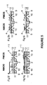
- Figures 5a to 5i illustrate by means of schematic cross-sections subsequent steps in a process flow for fabricating a semiconductor device according to an embodiment of the present invention.
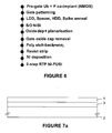
- Figure 6 shows a flowchart illustrating a fabrication process as illustrated in Figures 4a to 5i.
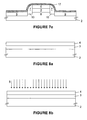
- Figures 7a to 7e show schematic cross-sections illustrating subsequent steps of a process flow for fabricating a semiconductor device according to an embodiment of the present invention.
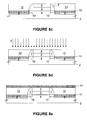
- Figures 8a to 8e show schematic cross-sections illustrating subsequent steps of a process flow for fabricating a semiconductor device according to an embodiment of the present invention.
- Figures 9a to 9d show schematic cross-sections illustrating subsequent steps of a process flow for fabricating a semiconductor device according to an embodiment of the present invention.
- Figures 10a to 10e show schematic cross-sections illustrating subsequent steps of a process flow for fabricating a semiconductor device according to an embodiment of the present invention.
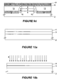
- Figures 11a to 11d illustrate by means of schematic cross-sections subsequent steps from a process flow according to an embodiment subsequent steps in a process flow for fabricating a semiconductor device according to an embodiment of the present invention.
- Figures 12a to 12d illustrate by means of schematic cross-sections subsequent steps from a process flow according to an embodiment subsequent steps in a process flow for fabricating a semiconductor device according to an embodiment of the present invention.
- devices structures such as transistors. These are three-terminal devices having a first main electrode such as a drain, a second main electrode such as a source and a control electrode such as a gate for controlling the flow of electrical charges between the first and second main electrodes.
- first main electrode such as a drain
- second main electrode such as a source
- control electrode such as a gate for controlling the flow of electrical charges between the first and second main electrodes.
- the invention is not limited thereto.
- the embodiments may be applied to other device structures such as metal-insulator-metal capacitors or to memory devices such as DRAM or non-volatile memories.
- the present invention provides a semiconductor device comprising a main electrode, e.g. a gate electrode, which comprises a material with a particular work function, e.g. a metal or metal silicide, and a method for manufacturing such a semiconductor device.
- a main electrode e.g. a gate electrode
- a material with a particular work function e.g. a metal or metal silicide
- the term "transistor” is intended to refer to a semiconductor device comprising a semiconductor channel region which is dielectrically coupled to a gate electrode via a gate dielectric.
- the semiconductor channel region is contacted at opposite sides by a source junction and a drain junction.
- Various types of transistor architectures are already known in the art.
- Planar gate devices can be formed on a bulk semiconductor substrate or on a semiconductor-on-insulator substrate.
- the channel of the device is controlled by the gate electrode from multiple sides.
- the body of semiconductor material wherein the channel is formed is made as thin as possible to allow a more efficient control by the gate electrode.
- the body of a fin-FET may have a thickness in the range of between 10 nm and 100 nm. In 32 nm technology for example the fin width may be in the range of between 10 nm and 20 nm.
- the "substrate” may include a semiconductor substrate such as e.g. a silicon (Si), a gallium arsenide (GaAs), a gallium arsenide phosphide (GaAsP), an indium phosphide (InP), a germanium (Ge) or a silicon germanium (SiGe) substrate.
- the "substrate” may include for example, an insulating layer such as a SiO 2 or a Si 3 N 4 layer in addition to a semiconductor substrate portion.
- substrate also includes semiconductor-on-insulator substrates such as silicon-on-glass, silicon-on sapphire substrates, silicon-on-insulator(SOI) substrates, germanium-on-insulator substrates (GOI).
- semiconductor-on-insulator substrates such as silicon-on-glass, silicon-on sapphire substrates, silicon-on-insulator(SOI) substrates, germanium-on-insulator substrates (GOI).
- substrate is thus used to define generally the elements or layers that underlie a layer or portions of interest. Accordingly, a substrate may be a wafer such as a blanket wafer or may be a layer applied to another base material, e.g. an epitaxial semiconductor layer grown onto a lower layer.
- crystalline substrate is intended to include various forms of crystalline material, such as monocrystalline or microcrystalline.
- silicide or “metal silicide” is meant a compound formed of one or more metals with a semiconductor material, such as silicon, germanium or silicon-germanium.
- a semiconductor material such as silicon, germanium or silicon-germanium.
- the terms “silicide”, “silicided”, “silicidation” or similar terms can refer to the reaction between a metal and silicon, but is not intended to be limited to silicon.
- the reaction of a metal with germanium, or any other suitable semiconductor material such as silicon-germanium may still be referred to as silicidation.
- Silicides may easily be formed by a thermal reaction of a variety of metals with silicon. Silicides may typically be formed in a two step process, i.e.
- first thermal treatment at a first temperature and a second thermal treatment at a second temperature higher than the first temperature.
- unreacted metal may selectively be removed.
- the second thermal step may be to reduce the sheet resistance of the silicide and/or to obtain a complete silicidation of the semiconductor material in contact with the silicide.
- the thermal treatment may preferably be done using rapid thermal processing.
- the parameters of the thermal process e.g. time and temperature, are selected in view of the silicide to be formed.
- a fully silicided (FUSI) gate electrode is formed by a reaction between silicide-forming metals and the semiconductor gate electrode, thereby fully consuming the semiconductor material of the gate electrode.
- a semiconductor device comprising a main electrode, e.g. a gate electrode, and a dielectric, e.g. gate dielectric, in contact with the main electrode, e.g. gate electrode, the main electrode, e.g. gate electrode comprising a material having a work function and a work function modulating element for modulating the work function of the material of the main electrode, e.g. gate electrode, towards a predetermined value.
- the main electrode, e.g. gate electrode furthermore comprises a diffusion preventing dopant element for preventing diffusion of the work function modulating element towards and/or into the dielectric, e.g. gate dielectric.
- predetermined value of a workfunction is meant a suitable value required or desired so as to obtain a p-type or an n-type device (see further).
- MOSFET transistor MOSFET transistor
- FIG. 1 shows a schematic cross-section of a MOSFET device 1 according to an embodiment of the invention.
- the MOSFET device 1 may be formed using a method according to an embodiment of the invention as will be described hereafter.
- standard CMOS processes known by a person skilled in the art may be used for process steps such as e.g. depositing layers or implanting ions.
- the MOSFET device 1 comprises a gate stack formed of a gate dielectric 3 and a fully silicided (FUSI) gate electrode 4, the FUSI gate electrode 4 comprising an alloy of a semiconductor material, e.g. silicon, germanium or silicon-germanium, and a suitable silicide-forming metal. According to another embodiment the gate electrode 4 may be formed of a metal.
- the MOSFET device 1 may be formed on a substrate 2. In the substrate 2 lowly doped junction regions 10 may be present which are aligned to the gate stack 3, 4. The MOSFET device 1 may furthermore comprise sidewall spacers 7 against sidewalls of the gate stack 3, 4.
- These sidewall spacers 7 may comprise a dielectric material such as, for example, silicon oxide, silicon nitride, silicon carbide or a combination thereof. Aligned to the sidewall spacers 7 highly doped junction regions 9 may be present in the substrate 2. The lowly doped regions 10 and the highly doped regions 9 may form source and drain regions of the MOSFET device 1. The source and drain regions may be formed on opposite sides of a channel region 8.
- the gate electrode 4 may be a fully silicided gate electrode 3 comprising an alloy of semiconductor material with a silicide-forming metal. According to other embodiments of the invention, the gate electrode 3 may be formed of a metal.
- the material of the gate electrode 3 has a particular work function.
- Gate electrode 3 further comprises a work function modulating element 6 for modulating the work function of the material of the gate electrode as well as a diffusion preventing dopant element 5 for preventing diffusion of the work function modulating element 6 toward the gate dielectric 3.
- the work function modulating element 6 is selected to tune the work function of the material of the gate electrode, for instance metal silicide or metal, towards a selected, predetermined value.
- the diffusion preventing dopant element 5 is selected to interact with the work function modulating element 6 such that this work function modulating element 6 does not substantially diffuse towards and/or into the gate dielectric 3.
- the MOSFET device 1 comprises a FUSI or metal gate electrode 4 in contact with a gate dielectric 3.
- the gate electrode 4 is a FUSI gate electrode
- the electrode may comprise a semiconductor material such as silicon, germanium or silicon-germanium, a silicide-forming metal, a first dopant element referred to as diffusion preventing dopant element 5 and a second dopant element referred to as a work function modulating element 6.
- the work function modulating element 6 is selected to shift the work function of the material of the gate electrode 4, in the example given the work function of the metal silicide, towards a predetermined value, e.g.
- the diffusion preventing dopant element 5 and the work function modulating element 6 are selected to interact with each other such that diffusion of at least one of the diffusion preventing dopant element 5 and the work function modulating element 6 towards the gate dielectric 3 is impeded. If only a work function modulating element 6 would be provided to the gate electrode 4, the work function modulating element 6 would tend to diffuse towards the gate dielectric 3.
- this diffusion of the work function modulating element 6 may be prevented by interaction between both elements 5, 6. Therefore, preferably the diffusion preventing dopant element 5 and the work function modulating element 6 may be provided in a 1:1 ratio, or in other words the concentration of the diffusion preventing dopant element 5 and the work function modulating element 6 may be substantially equal to each other. Both the work function modulating element and the diffusion preventing dopant element apply forces to each other so as to help each other to stay within the gate electrode.
- the diffusion preventing dopant element 5 and the work function modulating element 6 are selected to interact with each-other such that the final dopant distributions close to the interface between the gate electrode 4 and the gate dielectric 3 is modulated and the number of interface states at that interface is reduced.
- a suitable metal for silicidation may be a metal such as nickel or platinum or may be a refractory metal such as cobalt, tungsten or titanium.
- the material may be selected to yield a silicide having an n-type work function.
- the work function of the silicide may then have a value from about the middle of the energy gap of the semiconductor material which is to be silicided to about the bottom of the conduction band thereof. For example, if silicon is used as a semiconductor material, the work function of the silicide ranges from about 4.2eV to about 4.7eV.
- a p-type MOSFET device 1 If a p-type MOSFET device 1 is to be fabricated, suitable metals are selected to yield a silicide having a p-type work function.
- the work function of the silicide may then have a value from about the middle of the energy gap of the semiconductor material which is to be silicided to about the top of the valence band thereof.
- the work function of the silicide ranges from about 4.7eV to about 5.2eV.
- the work function of the silicide may have a value about halfway the bottom of the conduction band and the top of the valence band with a variation of 10%.
- a midgap material may be obtained which is suitable to be used for n-type devices and for p-type devices. Furthermore, because the difference in work function of the gate and of the channel is reduced, the threshold voltage V t of the device may also be reduced. If silicon is used as a semiconductor material the work function of the silicide preferably is about 4.7eV ⁇ 0.2eV.
- the type and the concentration of work function modulating element 6 is selected depending on the required work function of the silicide formed and on the work function desired for the type of MOSFET device.
- the concentration of work function modulating element 6 may vary from 1e14 cm -3 to 1e16 cm -3 .
- a nickel silicide FUSI gate 4 typically a work function value of about 4.7 eV may be obtained.
- This work function can be tuned to be closer to the conduction band of silicon i.e. towards a value of 4.1eV, if an n-type MOSFETs is to be fabricated.
- Such a lowering in work function can be obtained by doping the nickel silicide with elements such as a lanthanide, e.g. Ytterbium (Yb), or elements such as Arsenic (As), Antimony (Sb) or Phosphorus (P).
- H.Y. Yu et al discloses in "Modulation of the Ni FUSI work function by Yb doping: from midgap to n-type band-edge" in technical digest IEDM meeting 2005, p630-633 , in figure 3(b) and the corresponding paragraph on page 601, that the value of the work function of nickel silicide can be varied from about 4.7eV to about 4.2eV by varying the ratio of Yb to Ni. Furthermore, the work function can be tuned to a value closer to the valence band of silicon i.e. towards a value of 5.2eV, for instance in case a p-type MOSFET is to be fabricated. Such a shift in the value of the work function can be obtained by doping the nickel silicide of gate 4 with elements such as Platinum (Pt) or boron (B).
- Pt Platinum
- B boron
- the diffusion preventing dopant element 5 may be selected from the group of Phosphorus (P), Silicon (Si), Germanium (Ge), Arsenic (As), Tin (Sn), or Antimony (Sb).
- the concentration of diffusion preventing dopant element 5 can vary from 1e14 cm -3 to 1e16 cm -3 .
- the concentration of diffusion preventing dopant element 5 may be substantially equal to the concentration of work function modulating element 6.
- an n-type MOSFET device may be formed wherein the gate electrode 4 comprises a low work function metallic alloy comprising at least one lanthanide as work function modulating element 6, a suitable metal for silicidation, a diffusion preventing dopant element 5 retarding or substantially preventing the diffusion of a lanthanide towards and/or into the gate dielectric 3 and a semiconductor material, the semiconductor comprising Si, Ge or SiGe.
- the lanthanides may comprise 15 elements from lanthanum to lutetium in the periodic table, including lanthanum (La), cerium (Ce), praseodymium (Pr), neodymium (Nd), promethium (Pm), samarium (Sm), europium (Eu), gadolinium (Gd), terbium (Tb), dysprosium (Dy), holmium (Ho), erbium (Er), thulium (Tm), ytterbium (Yb) and lutetium (Lu).
- La lanthanum
- Ce cerium
- Pr praseodymium
- Nd neodymium
- Pm promethium
- Sm samarium
- Eu europium
- Gd gadolinium
- Tb terbium
- Dy dysprosium
- Ho holmium
- Er erbium
- Tm thulium
- Yb yt
- the lanthanide may be Yb.
- the metal may be Ni.
- the semiconductor material may be Si.
- the gate electrode 4 may comprise Yb, Ni and/or Si.
- the diffusion preventing dopant element also referred to as diffusion-retarding element
- diffusion-retarding element may be phosphorus (P).
- Figure 2 shows the gate capacitance (Cgb(F)) in function of the gate voltage (Vgb(V)), in curves measured for a capacitor structure comprising a prior art Yb-doped NiSi FUSI electrode (curve 20) and for a Yb+P-doped NiSi FUSI electrode according to an embodiment of the present invention (curve 21).
- a bump is observed in the capacitance-voltage curve as indicated by the dotted ellipse indicated by reference number 19.
- This bump 19 is indicative for the presence of interface states D it at the interface between the gate electrode 4 and the gate dielectric 3.
- Such a bump 19 is not observed in case an Yb+P-doped NiSi FUSI electrode according to an embodiment fo the present invention. In that case, the capacitance value varies smoothly with the applied voltage in the negative voltage range.
- Figure 3 shows the gate current density (Jgb) vs. the gate voltage (Vgb) in curves obtained for a capacitor structure comprising a prior art NiSi FUSI gate electrode (curve 22) and for a prior art Yb-doped NiSi FUSI gate electrode. From this figure it is clear that if a prior art Yb-doped NiSi FUSI gate electrode is used (curve 23) the gate leakage current is increased compared to a prior art NiSi FUSI gate electrode without Yb (curve 22).
- the thickness of the silicon layer used to form the NiSi was varied from 100 nm to 40 nm, while a concentration of 4e15/cm 2 Yb was implanted with implant energies of 20 keV or 30 keV. If however a Yb+P doped NiSi FUSI electrode according to an embodiment of the invention is used, the increase in gate leakage current can be limited.
- Figure 4 compares the gate capacitance (Cgb) vs. gate voltage (Vgb) characteristic obtained for a capacitor structure comprising a prior art NiSi FUSI gate electrode (curve 24), for a prior art Yb-doped NiSi FUSI gate electrode (curve 25), for a prior art P-doped NiSi FUSI gate electrode (curve 26) and for an Yb+P doped NiSi FUSI electrode according to an embodiment of the invention (curve 27).
- the largest shift in threshold voltage as indicated by the shift in the characteristics is obtained with the device with an Yb-doped NiSi FUSI gate electrode (curve 25).
- FIG. 5a to 5i and Fig. 6 illustrate subsequent steps in a method for forming a MOSFET device 1 according to embodiments of the invention.
- the MOSFET device 14 may comprise a fully silicided gate electrode 4.
- the fabrication process illustrated that the method according to embodiments of the invention allows combining the fabrication of an n-type MOSFET device with a type MOSFET device on a same substrate 2.
- an n-type MOSFET device is fabricated while on the right side of the substrate 2 a p-type MOSFET device is fabricated.
- the substrate 2 may comprise active regions NMOS and PMOS on which the respective MOSFET devices will be fabricated. These active regions are isolated from each other by dielectric regions 13, preferably formed using shallow-trench-isolation (STI) whereby grooves formed in the substrate 2 are filled with one or more dielectric layers.
- STI shallow-trench-isolation
- the gate dielectric layer 3 can be a silicon-oxide, a silicon oxynitride or a high-k dielectric such as hafnium silicates or hafnium oxides.
- the gate dielectric 3 may preferably be a silicon oxynitride layer.
- the gate electrode layer 4 can be formed of a semiconductor material.
- the thickness of the semiconductor layer 4 may be in the range of between 20 nm to 150 nm, and may, for example, be 100 nm.
- the semiconductor material may be silicon, such as polycrystalline silicon, or may be germanium or silicon-germanium.
- a capping layer 14 can be formed (not illustrated as a separate layer in Fig. 5a) which can removed selectively with respect to the semiconductor layer 4.
- This capping layer may be a silicon-germanium layer.
- a stop layer 15 can be formed which can be selectively removed with respect to the other layers on the substrate 2. This stopping layer 15 is used as a stopping layer in a chemical-mechanical processing step.
- the stopping layer 15 may be a silicon nitride layer.
- Ytterbium (Yb) 6 is implanted in the gate electrode layer 4, in the example given in the semiconductor layer 4, as indicated by the arrows in Figure 5a. This may be done uniformly. Preferably, at this stage, Yb is only implanted in that part of the semiconductor layer 4 where an NMOS is to be formed. As shown in Figure 5a a protective layer 16 such as a photoresistive layer may then be formed on the area where a PMOS devices is to be formed.
- the Yb implant dose may be in the range of between 1e15 cm -3 and 1e16cm -3 , and may for example be 4e15cm -3 .
- the Yb implant energy may be in the range of between 5 keV and 40 keV, or in the range of between 20 keV and 40 keV.
- the diffusion preventing dopant element 5 is implanted in the NMOS part of the gate electrode layer 4, as indicated by the arrows in Figure 5b.
- Ion implantation may be used to implant the diffusion preventing dopant element 5 in the gate electrode layer 4.
- this diffusing preventing dopant element 5 may be P.
- the P implant dose preferably may be the range of between 1e15 cm -3 and 1e16cm -3 , and may for example be 4e15cm -3 .
- the P implant energy may be in the range of 5 keV to 15 keV, or in the range of between 6 keV to 10 keV.
- the protective layer 16 may be removed. This may be done by any suitable technique known by a person skilled in the art.
- the gate stack 3, 4, 14, 15 may be patterned.
- lowly doped junction regions 10 may be formed aligned to the gate stack 3, 4, 14, 15.
- Sidewall spacers 7 may then be formed against the sidewalls of the gate stack 3, 4, 14, 15.
- These sidewall spacers 7 may be formed of a dielectric material such as silicon oxide, silicon nitride, silicon carbide or a combination thereof.
- Aligned to the sidewall spacers 7 highly doped junction regions 9 may be formed in the substrate 2.
- the lowly doped regions 10 and the highly doped regions 9 may form the source and drain regions of the MOSFET device and may be formed on opposite sides of a channel region 8.
- a thermal treatment, such as a spike anneal can be performed after the implantation step to form the lowly doped regions 10 and the highly doped regions 9.
- a layer of nickel is deposited over the substrate 2 followed by silicidation of the semiconductor material of the gate electrode 4.
- the exposed source and drain 9 regions are silicided.
- Preferably about 10 to 50nm nickel is deposited.
- the Ni layer may, for example, have a thickness of 10 nm.
- the temperature can range from 150°C to 350°C, for a period of between 10s and 5 minutes.
- the temperature of the first thermal step may 300°C during a time period of 30s.
- the unreacted nickel may be removed by, for example, using a wet etch such as HCl comprising etching.
- a second thermal step may be performed. In this second thermal step, the temperature may range from 300°C to 550°C for a period of between 10s and 5 minutes.
- the temperature of the second thermal step may be 470°C for a time period of 30s.
- a planarizing layer 12 may then be deposited over the substrate 2 (see Figure 5c).
- the planarizing layer 12 may be a silicon oxide layer deposited using, for example, chemical vapour deposition (CVD).
- the planarizing layer 12 may be polished by e.g. using chemical-mechanical-polishing (CMP).
- CMP chemical-mechanical-polishing
- the polishing stops when the stopping layer 15 is reached.
- a dry etch is then further used to uniformly remove the planarizing layer 12 whereby the stopping layer 15 protects the underlying semiconductor gate electrode 4.
- the stopping layer 15 may then be removed, for example by using a dry etch process, as is shown in figure 5d.
- the capping layer 14 may be removed as well, for example by using a dry etch process.
- the semiconductor gate electrodes 4 of the n-type MOSFET (left) and p-type MOSFET (right) are thereby exposed.
- the thickness of the semiconductor layer 4 and of the capping layer 14 may be chosen such that their combined thickness in the NMOS region equals their combined thickness in the PMOS region. However the ratio semiconductor layer thickness to capping layer thickness may be different in the NMOS region with respect to the PMOS region.
- a protective layer 16 may be formed over the NMOS region.
- the protective layer 16 may be a photosensitive layer.
- the exposed semiconductor gate electrode 4 of the p-type MOSFET may partially be removed, for example by using a dry etch, to reduce the thickness of the semiconductor gate electrode 4 from for example 100 nm to between 30 nm to 50 nm.
- the protective layer 16 may be removed.
- a layer of silicide-forming metal 17 may then be deposited over the structure.
- the metal layer 17 may be a nickel or a nickel alloy layer.
- the metal layer 17 may have a thickness of between 10 nm to 150 nm, or between 40 nm and 80 nm, an may for example be 60 nm.
- a first thermal process step may be performed to have the deposited metal layer 17 react with the P- and Yb- doped nMOS semiconductor gate electrode 4 and with the pMOS semiconductor gate electrode 4.
- the temperature can range from 250°C to about 450°C, for a period of between 10s and 5 minutes.
- the temperature of the first thermal step may be 370°C for a time period of 30s.
- the unreacted metal 17 may be selectively removed, for example by using a wet etch.
- the pMOS gate electrode 4 will already be fully silicided during the first thermal step and a metal-rich silicide will be obtained.
- the nMOS gate electrode 4 will only be partially silicided, leaving a semiconductor portion adjacent to the gate dielectric 3.
- the partially silicided gate nMOS gate electrode 4 may become fully silicided as the un-silicided bottom portion of the nMOS gate electrode will also react with the silicide-forming metal in the silicided portion.
- a fully silicided nMOS gate electrode 4 may be obtained with a metal-to-semiconductor ratio lower then for the fully silicided pMOS gate electrode 4.
- FIG. 7a Another embodiment of the method according to the present invention is illustrated in figures 7a to 7e.
- a substrate 2 is provided on which a gate stack formed of a gate dielectric layer 3 and a gate electrode layer 4 is provided.
- the gate dielectric layer 3 can be a silicon-oxide, a silicon oxynitride or a high-k dielectric such as hafnium silicates or hafnium oxides.
- the gate electrode layer 4 may be formed in semiconductor material.
- the semiconductor material may be silicon, such as polycrystalline silicon, or may be germanium or silicon-germanium.
- a diffusion preventing dopant element 5 is incorporated in the gate electrode 4.
- the diffusion preventing dopant element 5 is selected to modulate, i.e. to substantially prevent or at least retard, the diffusion of the work function modulating element 6 from the silicided gate 4 towards and/or into the gate dielectric 3.
- a ytterbium nickel silicide is to be formed, preferably phosphorus may be incorporated in the gate electrode 4.
- ion implantation may be used.
- a work function modulating element 6 is incorporated in the gate electrode 4. This is indicated with the arrows in Figure 7c. This work function modulating element 6 will later react with the silicide-forming metal 17 and the semiconductor gate electrode 4 to form a fully silicided gate electrode 4.
- the diffusion preventing dopant element 5 is introduced into the semiconductor gate electrode 4 prior to introduction of the work function modulating element 6, the invention is not limited hereto. According to other embodiments of the invention, first the work function modulating element 6 is introduced and subsequently the diffusion preventing dopant element 5 is introduced.
- the stack formed of the gate dielectric 3 and the semiconductor gate electrode 4 comprising the diffusion preventing dopant element 5 and the work function modulating element 6 is patterned to form the gate stack of a MOSFET device 1.
- the region in the substrate 2 which is under dielectric control of the gate electrode 4 will form the channel region 8 of the transistor.
- the processing of the MOSFET device is continued by forming in the substrate 2, highly doped regions 9 and lowly doped regions 10 aligned to the gate stack formed by the gate dielectric 3 and gate electrode 4.
- the doped regions 9, 10 can be formed by, for example, ion implantation.
- Sidewall spacers 7 may be formed against sidewalls of the gate stack 3, 4.
- a layer of nickel may then be deposited over the substrate 2.
- the exposed highly doped regions 9 may be silicided.
- a layer of silicide-forming metal 17 is deposited over the substrate 2 as shown in Figure 7e.
- the thickness of this metal layer 17 may be selected to yield a fully silicided gate electrode 4.
- the silicide-forming metal 17 will react with the semiconductor material comprising the work function modulating element 6 and the diffusion preventing dopant element 5 to form a silicide 11.
- the semiconductor material of the substrate 1 is silicon, germanium or silicon-germanium
- silicide 11 may also be formed at the doped regions 9.
- thermal processing to form the silicide 11 may be done as follows. Firstly, a first thermal step is performed, e.g. an annealing step. Then unreacted metal 17 is selectively removed. Optionally a second thermal step may be performed to, for example, reduce the sheet resistance of the silicide formed during the first thermal step or to fully silicidize the gate electrode 4 if necessary.
- the step of fully siliciding the semiconductor material of the gate electrode 4 may thus comprise the step of providing a thermal budget to convert substantially all the semiconductor material into a silicide 11 and the step of removing any unreacted metal. Finally a MOSFET device 1 is obtained as shown in Figure 1.
- FIG. 8a A further embodiment of the method according to the present invention is illustrated in Figures 8a to 8e.
- a substrate 2 is provided on which a stack of a gate dielectric layer 3 and a gate electrode layer 4 is formed.
- the gate dielectric layer 3 can be a silicon-oxide, a silicon oxynitride or a high-k dielectric such as hafnium silicates or hafnium oxides.
- the gate electrode layer 4 may be formed of a semiconductor material.
- the semiconductor material can be silicon, such as polycrystalline silicon, or can be germanium or silicon-germanium.
- a diffusion preventing dopant element 5 is incorporated in the gate electrode 4, as indicated by the arrows.
- This diffusion preventing dopant element 5 may be selected to modulate, i.e. to substantially prevent, or retard the diffusion of the work function modulating element 6 from the silicided gate 4 towards and/or into the gate dielectric 3.
- phosphorus may be incorporated in the gate electrode 4. Ion implantation may be used to introduce the diffusion preventing dopant element 5 in the gate electrode layer 4.
- the stack of the gate dielectric 3 and the semiconductor gate electrode 4 comprising the diffusion preventing dopant element 5 may be patterned to form the gate stack 3, 4 of a MOSFET device 1.
- the region in the substrate 2 which is under dielectric control of the gate electrode 4 may form the channel region 8 of the device 1.
- the processing of the MOSFET device 1 according to the present embodiment may be continued by forming in the substrate 2 lowly and highly doped regions 9, 10 aligned to the gate stack 3, 4.
- lowly doped regions 10 may be formed in the substrate 2 aligned to the gate stack 3, 4.
- Sidewall spacers 7 may be formed against sidewalls of the gate stack 3, 4.
- Highly doped regions 9 may be formed in the substrate 2.
- These doped regions 9, 10 may, for example, be formed by ion implantation.
- a layer of nickel may then be deposited over the substrate 2. In a two step thermal process the exposed highly doped regions 9 may be silicided.
- a planarizing layer 12 may then be deposited over the structure.
- the planarization layer 12 may be a silicon oxide layer deposited using chemical vapour deposition (CVD).
- the planarization layer 12 can be planarized using chemical-mechanical polishing until the semiconductor gate electrode 4 is exposed (see Figure 8d).
- a work function modulating element 6 is incorporated in the exposed semiconductor gate electrode 4. This may be done by, for example, ion implantation. This work function modulating element 6 will later react with the silicide-forming metal 17 and the semiconductor gate electrode 4 to form a fully silicided gate electrode 4.
- a layer of silicide-forming metal 17 may then be deposited as shown in Figure 8e.
- the thickness of this metal layer 17 may be selected to yield a fully silicided gate electrode 4.
- Silicidation may be performed by performing a thermal anneal process.
- the thermal anneal process may comprise a first anneal step. After this first anneal step, unreacted metal 17 may selectively be removed.
- a second thermal step may be performed to, for example, reduce the sheet resistance of the silicide formed during the first thermal step or to fully silicidize the gate electrode 4 if required.
- the step of fully siliciding the semiconductor material of the gate electrode 4 thus comprises the step of providing a thermal budget to convert substantially all the semiconductor material into a silicide and the step of removing any unreacted metal. Finally a MOSFET device 1 is obtained as shown in Figure 1.
- FIG. 9a A further embodiment of the method according to the present invention is illustrated by Figures 9a to 9d.
- a substrate 2 is provided on which a stack of a gate dielectric layer 3 and a gate electrode layer 4 is formed.
- the gate dielectric layer 3 can be a silicon-oxide, a silicon oxynitride or a high-k dielectric such as hafnium silicates or hafnium oxides.
- the gate electrode layer 4 may be formed of a semiconductor material.
- the semiconductor material may be silicon, such as polycrystalline silicon, or may be germanium or silicon-germanium.
- a diffusion preventing dopant element 5 is incorporated in the gate electrode 4.
- This diffusion preventing dopant element 5 is selected to modulate, i.e. to substantially prevent, or retard the diffusion of the work function modulating element 6 from the silicided gate 4 towards and/or into the gate dielectric 3.
- phosphorus may be incorporated in the gate electrode 4. Ion implantation may be used to introduce the diffusion preventing dopant element 5 in the gate electrode layer 4.
- the stack of the gate dielectric 3 and the gate electrode 4 comprising the diffusion preventing dopant element 5 may be patterned to form the gate stack 3, 4 of a MOSFET device 1.
- the region in the substrate 2 which is under dielectric control of the gate electrode 4 may form the channel region 8 of the device 1.
- the processing of the MOSFET device 1 may be continued by forming in the substrate 2 highly and lowly doped regions 9, 10 aligned to the gate stack 3, 4.
- lowly doped regions 10 may be formed in the substrate 2 aligned to the gate stack 3, 4.
- Sidewall spacers 7 may be formed against sidewalls of the gate stack 3, 4.
- Highly doped regions 9 may be formed in the substrate 2.
- These doped regions 9, 10 can be formed by, for example, ion implantation.
- a layer of nickel may then be deposited over the substrate 2.
- the exposed highly doped regions 9 may be silicided.
- a planarizing layer 12 may then be deposited over the structure.
- the planarization layer 12 may be a silicon oxide layer deposited using, for example, chemical vapour deposition (CVD).
- the planarization layer 12 can be planarized using chemical-mechanical polishing until the gate electrode 4 is exposed.
- a layer of a work function modulating element 6 may be deposited over the exposed semiconductor gate electrode 4.
- a layer of silicide-forming metal 17 may then be deposited over the layer of work function modulating element 6.
- the thickness of this metal layer 17 may be selected to yield a fully silicided gate electrode 4.
- the thermal processing comprises a first thermal step.
- the unreacted metal 8 and work function modulating element 6 may then selectively be removed.
- a second thermal step is performed to, for example, reduce the sheet resistance of the silicide formed during the first thermal step.
- the step of fully siliciding the semiconductor material of the gate electrode 4 thus comprises the step of providing a thermal budget to convert substantially all the semiconductor material into a silicide and the step of removing any unreacted metal. Finally a MOSFET device 1 is obtained as shown in Figure 1.
- FIG. 10a to 10d A further embodiment of method according to the invention is illustrated in Figures 10a to 10d.
- a substrate 2 is provided on which a stack of a gate dielectric layer 3 and a gate electrode layer 4 is formed.
- the gate dielectric layer 3 can be a silicon-oxide, a silicon oxynitride or a high-k dielectric such as hafnium silicates or hafnium oxides.
- the gate electrode layer 4 may be formed of a semiconductor material.
- the semiconductor material may be silicon, such as polycrystalline silicon, or may be germanium or silicon-germanium.
- a work function modulating element 6 is incorporated in the semiconductor layer 4 as indicated by the arrows. Ion implantation may be used to introduce the work function modulating element 6 in the semiconductor layer 4. This work function modulating element 6 will later react with the silicide-forming metal 17 and the material of the gate electrode 4 to form a fully silicided gate electrode 4.
- the stack of the gate dielectric 3 and the semiconductor gate electrode 4 comprising the work function modulating element 6 is patterned to form the gate stack 3, 4 of a MOSFET device 1.
- the region in the substrate 2 which is under dielectric control of the gate electrode 4 may form the channel region 8 of the transistor.
- the processing of the MOSFET device 1 may be continued by forming in the substrate 2 highly doped and lowly doped regions 9, 10 aligned to the gate stack of gate dielectric 3 and gate electrode 4.
- lowly doped regions 10 may be formed in the substrate 2 aligned to the gate stack 3, 4.
- Sidewall spacers 7 may be formed against sidewalls of the gate stack 3, 4.
- Highly doped regions 9 may be formed in the substrate 2.
- These doped regions 9, 10 can be formed by, for example, ion implantation.
- a layer of nickel is deposited over the substrate 2. In a two step thermal process the exposed source and drain 9 regions are silicided.
- a planarizing layer 12 may then be deposited over the structure.
- the planarizing layer 12 may be a silicon oxide layer deposited using chemical vapour deposition (CVD).
- the planarizing layer 12 can be planarized using chemical-mechanical polishing until the gate electrode 4 is exposed.
- a diffusion preventing dopant element 5 may be incorporated in the exposed semiconductor gate electrode 4.
- This dopant 5 is selected to modulate, i.e. to substantially prevent, or retard the diffusion of the work function modulating element 6 from the silicided gate 4 towards and/or into the gate dielectric 3.
- phosphorus may be incorporated in the gate electrode 4. Ion implantation may be used to introduce the diffusion preventing dopant element 5 in the gate electrode 4.
- a layer of silicide-forming metal 17 may be deposited over the layer of the work function modulating element 6.
- the thickness of this metal layer 17 may be selected to yield a fully silicided gate electrode 4.
- the thermal processing comprises a first thermal step.
- the unreacted metal 8 and element 6 are then selectively removed.
- a second thermal step is performed to, for example, reduce the sheet resistance of the silicide formed during the first thermal step.
- the step of fully siliciding the semiconductor material of the gate electrode 4 thus comprises the step of providing a thermal budget to convert substantially all the semiconductor material into a silicide and the step of removing any unreacted metal. Finally a MOSFET device 1 is obtained as shown in Figure 1.
- a substrate 2 is provided on which a stack of a gate dielectric layer 3 and a gate electrode layer 4 is formed.
- the gate dielectric layer 3 can be a silicon-oxide, a silicon oxynitride or a high-k dielectric such as hafnium silicates or hafnium oxides.
- the gate electrode layer 4 may be formed of a semiconductor material.
- the semiconductor material can be silicon, such as polycrystalline silicon, or can be germanium or silicon-germanium.
- the stack of the gate dielectric 3 and the semiconductor gate electrode 4 may be patterned to form the gate stack of a MOSFET device1.
- the region in the substrate 2 which is under dielectric control of the gate electrode 4 may form the channel region 8 of the device1.
- the processing of the MOSFET device 1 may then be continued by forming in the substrate 2 highly doped and lowly doped regions 9, 10 aligned to the gate stack 3, 4.
- lowly doped regions 10 may be formed in the substrate 2 aligned to the gate stack 3, 4.
- Sidewall spacers 7 may be formed against sidewalls of the gate stack 3, 4.
- Highly doped regions 9 may be formed in the substrate 2.
- These doped regions 9, 10 can be formed by, for example, ion implantation.
- a layer of nickel may be deposited over the substrate 2.
- the exposed highly doped regions 9 may be silicided.
- a planarizing layer 12 may then be deposited over the structure.
- the planarizing layer 12 may be a silicon oxide layer deposited using chemical vapour deposition (CVD).
- the planarizing layer 12 can be planarized using chemical-mechanical polishing until the gate electrode 4 is exposed.
- a diffusion preventing dopant element 5 is incorporated in the exposed gate electrode 4.
- This diffusion preventing dopant element 5 may be selected to modulate, i.e. to substantially prevent, or retard the diffusion of the work function modulating element 6 from the silicided gate 4 towards and/or into the gate dielectric 3.
- phosphorus may be incorporated in the gate electrode 4. Ion implantation may be used to introduce the diffusion preventing dopant element 5 in the gate electrode 4.
- a layer of a work function modulating element 6 may be deposited over the exposed gate electrode 4.
- a layer of silicide-forming metal 17 may then deposited over the layer of work function modulating element 6.
- the thickness of this metal layer 17 may be selected to yield a fully silicided gate electrode 4.
- the thermal processing comprises a first thermal step.
- the unreacted metal 17 and element 6 are then selectively removed.
- a second thermal step is performed to, for example, reduce the sheet resistance of the silicide formed during the first thermal step.
- the step of fully siliciding the semiconductor material of the gate electrode 4 thus comprises the step of providing a thermal budget to convert substantially all the semiconductor material into a silicide and the step of removing any unreacted metal. Finally a MOSFET device 1 is obtained as shown in Figure 1.
- the gate electrode layer 4 may comprise a metal or a stack of metal layers.
- metal instead of metal also conductive metal nitrides, metal oxides, metal carbides or metal silicon nitrides can be used.
- Examples of such conductive metals or metal-based materials suitable to be used for the gate electrode layer4 may be Ti, TiN, Ta, TaN, , TaC, TaCN, TaSiN, TiSiN, W, Mo.
- Such gate electrode stacks can comprise a metal-based layer with a thickness in the range of between 2 and 10 nm which may be capped with a polysilicon layer having a thickness in the range of between 40 nm and 100 nm.
- Figures 12a to 12d A possible implementation of this embodiment is illustrated in Figures 12a to 12d.
- a substrate 2 is provided on which a stack of a gate dielectric layer 3 and a gate electrode layer 4 is formed.
- the gate dielectric layer 3 can be a silicon-oxide, a silicon oxynitride or a high-k dielectric such as hafnium silicates or hafnium oxides.
- the gate electrode layer 4 may comprise a metal or a stack of metal layers, optionally capped with a polysilicon layer.
- a diffusion preventing dopant element 5 is incorporated in the gate electrode 4.
- This diffusion preventing dopant element 5 is selected to modulate, i.e. to substantially prevent, or retard the diffusion of the work function modulating element 6 from the metallic gate 4 towards and/or into the gate dielectric 3.
- a work function modulating element 6 is incorporated in the gate electrode 4.
- the diffusion preventing dopant element 5 is introduced into the gate electrode 4 prior to the work function modulating element 6 the invention is not limited hereto. According to other embodiments of the invention, first the work function modulating element 6 can be introduces and afterwards the diffusion preventing dopant element 5 can be introduced.
- the stack of the gate dielectric 3 and the gate electrode 4 comprising the diffusion preventing dopant element 5 and the work function modulating element 6 may be patterned to form the gate stack of a MOSFET device 1.
- the region in the substrate 2 which is under dielectric control of the gate electrode 4 may form the channel region 8 of the device 1.
- the processing of the MOSFET device 1 may then be continued by forming in the substrate 2 highly doped and lowly doped regions 9, 10 aligned to the gate stack 3, 4.
- lowly doped regions 10 may be formed in the substrate 2 aligned to the gate stack 3, 4.
- Sidewall spacers 7 may be formed against sidewalls of the gate stack 3, 4.
- Highly doped regions 9 can be formed in the substrate 2.
- These doped regions 9, 10 may be formed by ion implantation.
- the work function modulating element 6 and the diffusion preventing dopant element 5 may react.
- the work function modulating element 6 and the diffusion preventing dopant element 5 can be introduced respectively before and after patterning of the gate electrode 4 or vice versa.
- the work function modulating element 6 and the diffusion preventing dopant element 5 can both be introduced after patterning of the gate electrode 4. If one of the diffusion preventing dopant element 5 or the work function modulating element 6 is introduced after gate patterning then first a planarizing layer 12 may be deposited over the substrate 2 and may be patterned so as to expose the gate electrode 4. Thereafter the diffusion preventing dopant element 5 or the work function modulating element 6 may be introduced in the exposed gate electrode 4.
Landscapes
- Electrodes Of Semiconductors (AREA)
- Insulated Gate Type Field-Effect Transistor (AREA)
- Metal-Oxide And Bipolar Metal-Oxide Semiconductor Integrated Circuits (AREA)
- Thin Film Transistor (AREA)
Applications Claiming Priority (2)
| Application Number | Priority Date | Filing Date | Title |
|---|---|---|---|
| US85362806P | 2006-10-23 | 2006-10-23 | |
| US88434607P | 2007-01-10 | 2007-01-10 |
Publications (2)
| Publication Number | Publication Date |
|---|---|
| EP1916705A2 true EP1916705A2 (de) | 2008-04-30 |
| EP1916705A3 EP1916705A3 (de) | 2009-01-14 |
Family
ID=38924750
Family Applications (1)
| Application Number | Title | Priority Date | Filing Date |
|---|---|---|---|
| EP07075906A Withdrawn EP1916705A3 (de) | 2006-10-23 | 2007-10-23 | Halbleiterbauelement mit dotiertem Metall mit Hauptelektrode |
Country Status (4)
| Country | Link |
|---|---|
| US (1) | US20080136030A1 (de) |
| EP (1) | EP1916705A3 (de) |
| JP (1) | JP2008135726A (de) |
| CN (1) | CN101170127B (de) |
Cited By (1)
| Publication number | Priority date | Publication date | Assignee | Title |
|---|---|---|---|---|
| KR100986048B1 (ko) * | 2008-09-30 | 2010-10-08 | 한국과학기술원 | 비휘발성 메모리 소자 및 그 제조방법 |
Families Citing this family (17)
| Publication number | Priority date | Publication date | Assignee | Title |
|---|---|---|---|---|
| US8304342B2 (en) * | 2006-10-31 | 2012-11-06 | Texas Instruments Incorporated | Sacrificial CMP etch stop layer |
| WO2009133509A1 (en) * | 2008-04-29 | 2009-11-05 | Nxp B.V. | Integrated circuit manufacturing method and integrated circuit |
| JP4837011B2 (ja) * | 2008-09-18 | 2011-12-14 | 株式会社東芝 | 半導体装置、及び半導体装置の製造方法 |
| US9209180B2 (en) * | 2010-02-10 | 2015-12-08 | Taiwan Semiconductor Manufacturing Company, Ltd. | Field effect transistor with conduction band electron channel and uni-terminal response |
| CN102254805B (zh) * | 2010-05-19 | 2013-07-24 | 中国科学院微电子研究所 | 一种适用于nmos器件的金属栅功函数的调节方法 |
| CN102456558B (zh) * | 2010-10-25 | 2013-10-23 | 中芯国际集成电路制造(上海)有限公司 | 一种高介电常数介质-金属栅极的制造方法 |
| US8759178B2 (en) | 2011-11-09 | 2014-06-24 | Unisantis Electronics Singapore Pte. Ltd. | Method for manufacturing semiconductor device and semiconductor device |
| US8735971B2 (en) | 2011-12-02 | 2014-05-27 | Unisantis Electronics Singapore Pte. Ltd. | Method for producing semiconductor device and semiconductor device |
| US9117690B2 (en) | 2011-12-02 | 2015-08-25 | Unisantis Electronics Singapore Pte. Ltd. | Method for producing semiconductor device and semiconductor device |
| CN103377894B (zh) * | 2012-04-20 | 2016-09-21 | 中国科学院微电子研究所 | 金属硅化物制造方法 |
| US8877578B2 (en) * | 2012-05-18 | 2014-11-04 | Unisantis Electronics Singapore Pte. Ltd. | Method for producing semiconductor device and semiconductor device |
| US8697511B2 (en) | 2012-05-18 | 2014-04-15 | Unisantis Electronics Singapore Pte. Ltd. | Method for producing semiconductor device and semiconductor device |
| CN103594347B (zh) * | 2012-08-16 | 2016-12-21 | 中芯国际集成电路制造(上海)有限公司 | 一种半导体器件的形成方法 |
| CN103594346B (zh) * | 2012-08-16 | 2017-04-05 | 中芯国际集成电路制造(上海)有限公司 | 一种半导体器件的形成方法 |
| CN103632946B (zh) * | 2012-08-29 | 2016-03-16 | 中芯国际集成电路制造(上海)有限公司 | 全硅化物金属栅的形成方法 |
| US9082838B2 (en) * | 2012-09-28 | 2015-07-14 | Unisantis Electronics Singapore Pte. Ltd. | Method for producing a semiconductor device and semiconductor device |
| US9293502B2 (en) | 2013-07-26 | 2016-03-22 | Taiwan Semiconductor Manufacturing Company, Ltd. | Semiconductor switching device separated by device isolation |
Family Cites Families (12)
| Publication number | Priority date | Publication date | Assignee | Title |
|---|---|---|---|---|
| US5633177A (en) * | 1993-11-08 | 1997-05-27 | Advanced Micro Devices, Inc. | Method for producing a semiconductor gate conductor having an impurity migration barrier |
| US6030874A (en) * | 1997-01-21 | 2000-02-29 | Texas Instruments Incorporated | Doped polysilicon to retard boron diffusion into and through thin gate dielectrics |
| US5885861A (en) * | 1997-05-30 | 1999-03-23 | Advanced Micro Devices, Inc. | Reduction of dopant diffusion by the co-implantation of impurities into the transistor gate conductor |
| JP2002299610A (ja) * | 2001-03-30 | 2002-10-11 | Toshiba Corp | 半導体装置およびその製造方法 |
| US6803611B2 (en) * | 2003-01-03 | 2004-10-12 | Texas Instruments Incorporated | Use of indium to define work function of p-type doped polysilicon |
| US6890807B2 (en) * | 2003-05-06 | 2005-05-10 | Intel Corporation | Method for making a semiconductor device having a metal gate electrode |
| JP4439358B2 (ja) * | 2003-09-05 | 2010-03-24 | 株式会社東芝 | 電界効果トランジスタ及びその製造方法 |
| JP2005191482A (ja) * | 2003-12-26 | 2005-07-14 | Semiconductor Leading Edge Technologies Inc | 半導体装置及びその製造方法 |
| US7611943B2 (en) * | 2004-10-20 | 2009-11-03 | Texas Instruments Incorporated | Transistors, integrated circuits, systems, and processes of manufacture with improved work function modulation |
| US20060091483A1 (en) * | 2004-11-02 | 2006-05-04 | Doczy Mark L | Method for making a semiconductor device with a high-k gate dielectric layer and a silicide gate electrode |
| JP2006245417A (ja) * | 2005-03-04 | 2006-09-14 | Toshiba Corp | 半導体装置およびその製造方法 |
| US7504329B2 (en) * | 2005-05-11 | 2009-03-17 | Interuniversitair Microelektronica Centrum (Imec) | Method of forming a Yb-doped Ni full silicidation low work function gate electrode for n-MOSFET |
-
2007
- 2007-10-23 EP EP07075906A patent/EP1916705A3/de not_active Withdrawn
- 2007-10-23 JP JP2007275415A patent/JP2008135726A/ja active Pending
- 2007-10-23 US US11/977,027 patent/US20080136030A1/en not_active Abandoned
- 2007-10-23 CN CN2007101817414A patent/CN101170127B/zh active Active
Non-Patent Citations (4)
| Title |
|---|
| H.Y. YU ET AL.: "Modulation of the Ni FUSI work function by Yb doping: from midgap to n-type band-edge", TECHNICAL DIGEST IEDM, 2005, pages 630 - 633 |
| H.Y., YU: "Modulation of the Ni FUSI work function by Yb doping: from midgap to n-type band-edge", TECHNICAL DIGEST IEDM, 2005, pages 630 - 633 |
| PAWLAK M A ET AL: "MODULATION OF THE WORKFUNCTION OF NI FULLY SILICIDES GATES BY DOPING: DIELECTRIC AND SILICIDE PHASE EFFECTS", IEEE ELECTRON DEVICE LETTERS, IEEE SERVICE CENTER, NEW YORK, NY, US, vol. 27, no. 2, 1 February 2006 (2006-02-01), pages 99 - 101, XP001239565, ISSN: 0741-3106, DOI: 10.1109/LED.2005.862677 * |
| YU H Y ET AL: "Advanced Ni-based FUlly SIlicidation (FUSI) technology for sub-45nm CMOS devices", SOLID-STATE AND INTEGRATED CIRCUIT TECHNOLOGY, 2006. ICSICT '06. 8TH INTERNATIONAL CONFERENCE ON, IEEE, PI, 1 October 2006 (2006-10-01), pages 404 - 407, XP031045601, ISBN: 978-1-4244-0160-4 * |
Cited By (1)
| Publication number | Priority date | Publication date | Assignee | Title |
|---|---|---|---|---|
| KR100986048B1 (ko) * | 2008-09-30 | 2010-10-08 | 한국과학기술원 | 비휘발성 메모리 소자 및 그 제조방법 |
Also Published As
| Publication number | Publication date |
|---|---|
| EP1916705A3 (de) | 2009-01-14 |
| CN101170127A (zh) | 2008-04-30 |
| US20080136030A1 (en) | 2008-06-12 |
| JP2008135726A (ja) | 2008-06-12 |
| CN101170127B (zh) | 2013-03-06 |
Similar Documents
| Publication | Publication Date | Title |
|---|---|---|
| US20080136030A1 (en) | Semiconductor device comprising a doped metal comprising main electrode | |
| JP4473710B2 (ja) | 半導体装置 | |
| US7151023B1 (en) | Metal gate MOSFET by full semiconductor metal alloy conversion | |
| TWI364068B (en) | Nitrogen-containing field effect transistor gate stack containing a threshold voltage control layer formed via deposition of a metal oxide | |
| TWI411107B (zh) | 高效能金氧半場效電晶體 | |
| JP5041685B2 (ja) | 超急峻レトログレード・ウェル(ssrw)fetデバイスおよびその製造方法 | |
| US8629009B2 (en) | Programmable high-k/metal gate memory device | |
| JP2008135726A5 (de) | ||
| CN100452357C (zh) | 半导体装置及其制造方法 | |
| US7416967B2 (en) | Semiconductor device, and method for manufacturing the same | |
| US20070128785A1 (en) | Method and apparatus for fabricating cmos field effect transistors | |
| EP1916706B1 (de) | Verfahren zur Herstellung eines Halbleiterbauelements und auf diese Weise hergestelltes Halbleiterbauelement | |
| CN100472756C (zh) | 具有可调栅极功函数的双金属cmos晶体管以及其制法 | |
| US7504329B2 (en) | Method of forming a Yb-doped Ni full silicidation low work function gate electrode for n-MOSFET | |
| US20060289953A1 (en) | Semiconductor device and manufacturing method of the same | |
| JPWO2007148600A1 (ja) | 半導体装置およびその製造方法 | |
| US8344460B2 (en) | Method for forming a nickelsilicide FUSI gate | |
| US20090134469A1 (en) | Method of manufacturing a semiconductor device with dual fully silicided gate |
Legal Events
| Date | Code | Title | Description |
|---|---|---|---|
| PUAI | Public reference made under article 153(3) epc to a published international application that has entered the european phase |
Free format text: ORIGINAL CODE: 0009012 |
|
| AK | Designated contracting states |
Kind code of ref document: A2 Designated state(s): AT BE BG CH CY CZ DE DK EE ES FI FR GB GR HU IE IS IT LI LT LU LV MC MT NL PL PT RO SE SI SK TR |
|
| AX | Request for extension of the european patent |
Extension state: AL BA HR MK RS |
|
| RAP1 | Party data changed (applicant data changed or rights of an application transferred) |
Owner name: TAIWAN SEMICONDUCTOR MANUFACTURING COMPANY, LTD. ( Owner name: INTERUNIVERSITAIR MICROELEKTRONICA CENTRUM (IMEC) |
|
| PUAL | Search report despatched |
Free format text: ORIGINAL CODE: 0009013 |
|
| AK | Designated contracting states |
Kind code of ref document: A3 Designated state(s): AT BE BG CH CY CZ DE DK EE ES FI FR GB GR HU IE IS IT LI LT LU LV MC MT NL PL PT RO SE SI SK TR |
|
| AX | Request for extension of the european patent |
Extension state: AL BA HR MK RS |
|
| RAP1 | Party data changed (applicant data changed or rights of an application transferred) |
Owner name: TAIWAN SEMICONDUCTOR MANUFACTURING COMPANY, LTD. ( Owner name: IMEC |
|
| 17P | Request for examination filed |
Effective date: 20090714 |
|
| AKX | Designation fees paid |
Designated state(s): DE FR GB |
|
| 17Q | First examination report despatched |
Effective date: 20160212 |
|
| STAA | Information on the status of an ep patent application or granted ep patent |
Free format text: STATUS: THE APPLICATION IS DEEMED TO BE WITHDRAWN |
|
| 18D | Application deemed to be withdrawn |
Effective date: 20160623 |