EP1916675A1 - Bobinage comportant plusieurs branches de bobinage et micro-inductance comportant l'un des bobinages - Google Patents
Bobinage comportant plusieurs branches de bobinage et micro-inductance comportant l'un des bobinages Download PDFInfo
- Publication number
- EP1916675A1 EP1916675A1 EP07354055A EP07354055A EP1916675A1 EP 1916675 A1 EP1916675 A1 EP 1916675A1 EP 07354055 A EP07354055 A EP 07354055A EP 07354055 A EP07354055 A EP 07354055A EP 1916675 A1 EP1916675 A1 EP 1916675A1
- Authority
- EP
- European Patent Office
- Prior art keywords
- winding
- sections
- branches
- turns
- plane
- Prior art date
- Legal status (The legal status is an assumption and is not a legal conclusion. Google has not performed a legal analysis and makes no representation as to the accuracy of the status listed.)
- Granted
Links
Images


Classifications
-
- H—ELECTRICITY
- H01—ELECTRIC ELEMENTS
- H01F—MAGNETS; INDUCTANCES; TRANSFORMERS; SELECTION OF MATERIALS FOR THEIR MAGNETIC PROPERTIES
- H01F17/00—Fixed inductances of the signal type
- H01F17/0006—Printed inductances
- H01F17/0033—Printed inductances with the coil helically wound around a magnetic core
-
- H—ELECTRICITY
- H01—ELECTRIC ELEMENTS
- H01F—MAGNETS; INDUCTANCES; TRANSFORMERS; SELECTION OF MATERIALS FOR THEIR MAGNETIC PROPERTIES
- H01F17/00—Fixed inductances of the signal type
- H01F17/04—Fixed inductances of the signal type with magnetic core
Definitions
- the invention relates to a winding comprising a plurality of disjoint turns constituting a plurality of substantially parallel winding branches, each winding having a rectangular lower plane section in a lower plane, a rectangular upper plane section in an upper plane and two rising sections. , the rising sections of two adjacent branches disposed between the two adjacent branches being arranged alternately in a single plane.
- the invention is part of the theme of integrated micro-inductors for applications in power electronics. It can, more generally, apply to all inductive systems integrated or not (inductors, transformers, magnetic recording heads, actuators, sensors, etc ...) requiring a high density of electrical power.
- micro-inductances of various types For many years there have been micro-inductances of various types. However, the discrete components remain very predominantly used in applications using high power densities because only these allow to use very thick winding son to achieve very low levels of electrical resistance.
- Most of the micro-inductors used on the market are discrete components manufactured by micromechanical processes of micro-machining, gluing, micro-winding, etc. These processes are difficult to implement. work, individual treatment, flexible in terms of design and greatly limit the miniaturization of power circuits. In particular, the thickness of the discrete micro-inductors (typically greater than 0.5 mm) does not allow appropriate packaging in the power supply circuits currently used for mobile telephony, for example.
- the manufacturing techniques used in microelectronics allow a much greater flexibility in the implementation of different designs, provide a collective treatment and are compatible with the idea of miniaturization because the thickness (including substrate) can easily be less than 300 ⁇ m. However, they are poorly suited to deposition of high thicknesses (greater than 10 .mu.m) of conductive, magnetic or dielectric materials and to their etching after photolithography.
- Micro-inductances of the toroidal solenoid type have a good compromise between losses and level of inductance because they approach the ideal case of the infinite solenoid.
- the rising sections of two adjacent branches disposed between the two adjacent branches are arranged alternately in a single plane, which provides a small spacing between two adjacent branches.
- the compactness of the device can thus be increased. For these devices, it is sought to increase the level of inductance and to minimize losses.
- the object of the invention is to improve the performance of a micro-inductor, while increasing the compactness of the micro-inductance.
- this object is achieved by a winding according to the appended claims and more particularly by the fact that the upper and lower sections corresponding to one and the same turn are aligned with respect to one another and having a width greater than the width of the corresponding rising sections disposed between two adjacent winding branches, the turns fill almost all of the envelope surface of the winding, a minimum isolation gap separating the adjacent turns.
- the different types of winding described below can be made without necessarily using a magnetic core.
- the coil wraps around a magnetic core.
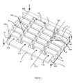
- the winding shown in Figures 1 to 3 comprises a plurality of turns 1 spaced apart from each other by a minimum separation gap 2 separating adjacent turns 1.
- the isolation gap 2 is set by the constraints of technological achievement and the desired electromagnetic behavior.
- the turns 1 constitute a winding around a magnetic core 3 having four parallel branches 11 (11a, 11b, 11c, 11d). One could also consider the same winding without magnetic core or with an open core.
- the plurality of disjointed turns 1 constitute a winding around substantially parallel branches 11 of the magnetic core 3. When this coil is used without a magnetic core, the disjoint turns 1 constitute a plurality of substantially parallel winding branches.
- Each turn 1 has a lower plane section 4 in a lower plane, an upper plane section 5 in an upper plane and two rising planar sections 12 and 13. It should be noted that these four elements (the lower plane section 4, the plane section upper 5 and the two planar rising sections 12 and 13) are not connected together so as to form a loop as, for example, in the case of a winding classical solenoid. Indeed, the flat sections 4 and 5 may belong to separate electrical conductors, each electrical conductor passing from the lower plane for a predetermined branch to the upper plane for an adjacent branch and vice versa. The turns 1 fill almost all the envelope surface of the winding, with the minimum isolation gap 2 near.
- the envelope surface of the coil means a continuous surface delimited by the coil and connecting the adjacent turns to each other.
- the envelope surface of the winding thus includes turns 1 and isolation gaps 2. This envelope surface of the winding must be filled to the maximum by the turns 1, the isolation gap 2 serving only to ensure the electrical insulation between the turns 1.
- the isolation gaps 2 can, moreover, be filled by a material insulating.
- the turns constitute a quasi-total envelope of the branches of the magnetic core 3.
- the micro-inductor uses all the space potentially available for winding and leaves no room for unused space.
- the micro-inductance thus has a lower resistance for a predetermined size.
- the thickness of the winding is a compromise between the ease of realization and the desired level of resistance.
- the rising sections 12a and 12b of two adjacent branches 11a and 11b disposed between the two adjacent branches 11a and 11b are arranged alternately (12a, 12b, 12a, 12b, ...) in a single plane.
- this single plane is perpendicular to the plane of the magnetic core 3 and passes through the axis CC which passes through the rising sections 12a and 12b.
- the turns 1 constitute an almost total envelope of the branches 11 of the magnetic core, a minimum isolation gap 2 separating adjacent turns 1.
- the turns 1 fill almost all the envelope surface of the winding, the winding being constituted by several winding branches, with or without magnetic core.
- the upper 5 and lower 4 sections represent, given their size, the bulk of the surface of the turns.
- the length Lm (FIG. 1) of the rising sections 12 is, for example, of the order of 20 microns
- the length Ls of the lower 4 and upper sections 5 is, for example, of the order of several hundred microns.
- the upper 5 and lower 4 sections preferably have a substantially rectangular shape (see FIGS. 1 to 4), to which are added connections to the rising sections 12.
- the upper section 5 advantageously has the same dimensions and, preferably, the same shape as the lower section 4 corresponding to the same turn 1 and they are preferably aligned relative to each other. Thus, they are superimposed completely, that is to say their projections in a plane parallel to the upper sections 4 and 5 are the same.
- the upper sections 4 and lower 5 have a width greater than the width of corresponding rising sections 12a and 12b disposed between two adjacent branches 11a and 11b.
- the width of the rising sections 12a and 12b disposed between two adjacent branches 11a and 11b is preferably less than half the width of the upper and lower sections 4 to allow entanglement of the turns at the crossings between the turns.
- the upper 5 and lower 4 sections have a width greater than the sum of the widths of the corresponding rising sections 12 disposed between two adjacent winding branches.
- the rising sections 12a and 12b have the same surface.
- the rising sections 13 disposed outside an outer branch 11a of the micro-inductor may have the same width as the upper 4 and lower 5 sections of the corresponding turns 1 of the same branch 11a.
- each turn 1 corresponding to the branch 11a (right in Figure 1) are connected by the rising sections 13 disposed outside.
- the upper 4 and lower 5 sections of each turn 1 corresponding to the branch 11d at the other end (left in Figure 1) of the core 3 are connected by the rising sections 12c disposed between the adjacent branches 11c and 11d.
- Two adjacent turns corresponding to the branch 11d at the end of the core 3 (shown on the left in FIG. 1) are connected by an upwardly mounted rising section 12d and a connection section 14 arranged in the lower plane corresponding to the sections lower 4.
- the sizing of this winding can be done in the following manner illustrated in FIG. 2.
- the length C of the magnetic core is defined. It will be considered that all the branches of the core are of the same width WMAG.
- the technological and electrical constraints set the dimensions V of the rising sections 12, the inter-turn distance INT and the spacing M between the coil and the magnetic circuit. It should be noted that FIG. 2 is not to scale and that the spacing M is, thus, variable in FIG. 2.
- the inter-turn distance INT between two adjacent turns corresponds to the difference 2 of minimum isolation.
- the winding can then be fully defined.
- the number of turns per N-branch (five in FIG. 2) is determined by the desired level of inductance.
- the thickness of conductive material is finally fixed as a compromise between the ease of realization and the desired level of resistance.
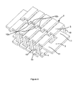
- FIG. 4 illustrates a micro-inductance with a substantially annular closed magnetic core 3 of which only two parallel branches 11 are covered by a winding constituting an almost total envelope of the two branches 11.
- the same type of winding as that previously described can be used.
- the particular embodiment makes it possible to improve the performance of the inductive systems and in particular to increase the inductance of the micro-inductance and the compactness of the winding.
- the turns constitute an almost complete envelope of the magnetic core on the entire parallel branches of the multi-branch core. Only the minimum isolation gaps 2 separate the lower planar sections 4 from two adjacent turns, the upper planar sections 5 from two adjacent turns and two adjacent rising sections. The minimum isolation gap 2 depends on the manufacturing technology used and the electromagnetic constraints. The gap between turns does not exceed the minimum isolation gap 2.
- the two variants do not present any additional manufacturing difficulties compared to the conventional pre-existing systems.
- the upper and lower sections 4 may respectively be etched in conductive layers.
Landscapes
- Engineering & Computer Science (AREA)
- Power Engineering (AREA)
- Microelectronics & Electronic Packaging (AREA)
- Coils Or Transformers For Communication (AREA)
- Coils Of Transformers For General Uses (AREA)
Abstract
Description
- L'invention est relative à un bobinage comportant une pluralité de spires disjointes constituant une pluralité de branches de bobinage sensiblement parallèles, chaque spire comportant une section plane inférieure rectangulaire dans un plan inférieur, une section plane supérieure rectangulaire dans un plan supérieur et deux sections montantes, les sections montantes de deux branches adjacentes disposées entre les deux branches adjacentes étant disposées en alternance dans un plan unique.
- L'invention s'inscrit dans la thématique des micro-inductances intégrées pour des applications en électronique de puissance. Elle peut, d'une manière plus générale, s'appliquer à tous les systèmes inductifs intégrés ou non (inductances, transformateurs, têtes d'enregistrement magnétique, actionneurs, capteurs, etc...) nécessitant une haute densité de puissance électrique.
- Il existe depuis de nombreuses années des micro-inductances de divers types. Cependant, les composants discrets restent très majoritairement utilisés dans des applications utilisant de fortes densités de puissance car seuls ces derniers permettent d'utiliser des fils de bobinage très épais permettant d'atteindre de très faibles niveaux de résistance électrique. La plupart des micro-inductances utilisées sur le marché sont des composants discrets fabriqués par des procédés micromécaniques de micro usinage, collage, micro-enroulement, etc... Ces procédés sont lourds à mettre en oeuvre, à traitement individuel, peu flexibles en termes de conception et limitent grandement la miniaturisation des circuits de puissance. En particulier, l'épaisseur des micro-inductances discrètes (typiquement supérieur à 0.5 mm) ne permet pas une mise en boîtier appropriée aux circuits d'alimentation utilisés actuellement pour la téléphonie mobile, par exemple.
- Les techniques de fabrications utilisées en microélectronique permettent une flexibilité bien plus grande au niveau de la mise en oeuvre de conceptions différentes, assurent un traitement collectif et sont compatibles avec l'idée de miniaturisation car l'épaisseur (substrat compris) peut facilement être inférieure à 300 µm. Cependant, elles sont mal adaptées au dépôt de fortes épaisseurs (supérieures à 10µm) de matériaux conducteurs, magnétiques ou diélectriques et à leur gravure après photolithographie.
- Pour les composants intégrés, on se heurte à des contraintes de réalisation technologique. En effet, des dépôts de couches conductrices ayant une épaisseur supérieure à 100 micromètres ne sont pour l'instant pas envisageable dans un procédé industriel standard.
- Des micro-inductances de type solénoïde torique présentent un bon compromis entre pertes et niveau d'inductance car elles s'approchent du cas idéal du solénoïde infini.
- L'article « Numerical Inductor Optimization » de A. von der Weth et al. (Trans. Magn. Soc. Japan, Vol.2, No.5, pp.361-366, 2002) décrit une micro-inductance avec un circuit magnétique ouvert composé d'une pluralité de noyaux parallélépipédiques. Une pluralité de spires disjointes constitue un bobinage autour des branches du noyau magnétique. Chaque spire comporte une section plane inférieure dans un plan inférieur, une section plane supérieure dans un plan supérieur et deux sections planes montantes.
- Les sections montantes de deux branches adjacentes disposées entre les deux branches adjacentes sont disposées en alternance dans un plan unique, ce qui permet d'obtenir un faible espacement entre deux branches adjacentes. La compacité du dispositif peut ainsi être augmentée. Pour ces dispositifs, on cherche à augmenter le niveau d'inductance et à minimiser les pertes.
- L'objet de l'invention consiste à améliorer les performances d'une micro-inductance, tout en augmentant la compacité de la micro-inductance.
- Selon l'invention, ce but est atteint par un bobinage selon les revendications annexées et plus particulièrement par le fait que les sections supérieure et inférieure correspondant à une même spire étant alignées l'une par rapport à l'autre et ayant une largeur supérieure à la largeur des sections montantes correspondantes disposées entre deux branches de bobinage adjacentes, les spires remplissent la quasi-totalité de la surface enveloppe du bobinage, un écart d'isolement minimum séparant les spires adjacentes.
- D'autres avantages et caractéristiques ressortiront plus clairement de la description qui va suivre de modes particuliers de réalisation de l'invention donnés à titre d'exemples non limitatifs et représentés aux dessins annexés, dans lesquels :
- les figures 1 à 3 représentent un mode de réalisation particulier de l'invention, respectivement en vue de perspective, en vue de dessus et en coupe vue de dessous selon le plan défini par les deux axes A-A et B-B de la figure 2,
- la figure 4 représente, en vue de perspective, un autre mode de réalisation particulier de l'invention.
- Les différents types de bobinage décrits ci-dessous peuvent être réalisés sans nécessairement utiliser un noyau magnétique. De préférence, cependant, le bobinage enveloppe un noyau magnétique.
- Le bobinage représentée aux figures 1 à 3 comporte une pluralité de spires 1 espacées les unes des autres par un écart 2 d'isolement minimum séparant les spires 1 adjacentes. L'écart 2 d'isolement est fixé par les contraintes de réalisation technologique et le comportement électromagnétique souhaité. Les spires 1 constituent un bobinage autour d'un noyau magnétique 3 comportant quatre branches parallèles 11 (11a, 11b, 11c, 11d). On pourrait également envisager le même bobinage sans noyau magnétique ou avec un noyau ouvert. La pluralité de spires 1 disjointes constituent un bobinage autour des branches 11 sensiblement parallèles du noyau magnétique 3. Lorsque ce bobinage est utilisé sans noyau magnétique, les spires 1 disjointes constituent une pluralité de branches de bobinage sensiblement parallèles.
- Chaque spire 1 comporte une section plane inférieure 4 dans un plan inférieur, une section plane supérieure 5 dans un plan supérieur et deux sections planes montantes 12 et 13. Il est à noter que ces quatre éléments (la section plane inférieure 4, la section plane supérieure 5 et les deux sections planes montantes 12 et 13) ne sont pas reliés entre eux de façon à former une boucle comme, par exemple, dans le cas d'un bobinage solénoïde classique. En effet, les sections planes 4 et 5 peuvent appartenir à des conducteurs électriques distincts, chaque conducteur électrique passant du plan inférieur pour une branche prédéterminée au plan supérieur pour une branche adjacente et inversement. Les spires 1 remplissent la quasi-totalité de la surface enveloppe du bobinage, à l'écart 2 d'isolement minimum près.
- On entend par surface enveloppe du bobinage une surface continue délimitée par le bobinage et reliant les spires adjacentes entre elles. La surface enveloppe du bobinage inclut ainsi les spires 1 et les écarts 2 d'isolement. Cette surface enveloppe du bobinage doit être remplie au maximum par les spires 1, l'écart 2 d'isolement servant uniquement à assurer l'isolation électrique entre les spires 1. Les écarts 2 d'isolement peuvent, par ailleurs être remplis par un matériau isolant.
- Ainsi, sur la figure 1, les spires constituent une enveloppe quasi-totale des branches du noyau magnétique 3. Contrairement aux dispositifs de l'art antérieur, la micro-inductance utilise toute la place potentiellement disponible pour le bobinage et ne laisse pas d'espace inutilisé. La micro-inductance a ainsi une résistance plus faible pour un encombrement prédéterminé.
- L'épaisseur du bobinage est un compromis entre la facilité de réalisation et le niveau de résistance désiré.
- Les sections montantes 12a et 12b de deux branches adjacentes 11a et 11b disposées entre les deux branches adjacentes 11a et 11b, sont disposées en alternance (12a, 12b, 12a, 12b,...) dans un plan unique. Dans le mode de réalisation particulier représenté à la figure 1, ce plan unique est perpendiculaire au plan du noyau magnétique 3 et passe par l'axe C-C qui passe par les sections montantes 12a et 12b. Les spires 1 constituent une enveloppe quasi-totale des branches 11 du noyau magnétique, un écart 2 d'isolement minimum séparant les spires 1 adjacentes.
- Ainsi, les spires 1 remplissent la quasi-totalité de la surface enveloppe du bobinage, le bobinage étant constitué par plusieurs branches de bobinage, avec ou sans noyau magnétique.
- Les sections supérieure 5 et inférieure 4 représentent, compte tenu de leur dimensions, l'essentiel de la surface des spires. Ainsi, tandis que la longueur Lm (figure 1) des sections montantes 12 est, par exemple, de l'ordre de 20 microns, la longueur Ls des sections inférieures 4 et supérieures 5 est, par exemple, de l'ordre de plusieurs centaines de microns. Les sections supérieure 5 et inférieure 4 ont, de préférence, une forme sensiblement rectangulaire (voire figures 1 à 4), à laquelle s'ajoute des raccords aux sections montantes 12. La section supérieure 5 a avantageusement les mêmes dimensions et, de préférence, la même forme que la section inférieure 4 correspondant à la même spire 1 et elles sont, de préférence, alignées l'une par rapport à l'autre. Ainsi, elles se superposent complètement, c'est-à-dire leurs projections dans un plan parallèle aux sections supérieure 4 et inférieure 5 sont les mêmes.
- Sur les figures 1-3, les sections supérieure 4 et inférieure 5 ont une largeur supérieure à la largeur des sections montantes 12a et 12b correspondantes disposées entre deux branches adjacentes 11a et 11b. La largeur des sections montantes 12a et 12b disposées entre deux branches adjacentes 11a et 11b est, de préférence, inférieure à la moitié de la largeur les sections supérieure 4 et inférieure 5 afin de permettre l'enchevêtrement des spires au niveau des croisements entre les spires. Ainsi, les sections supérieure 5 et inférieure 4 ont une largeur supérieure à la somme des largeurs des sections montantes 12 correspondantes disposées entre deux branches de bobinage adjacentes. Avantageusement, les sections montantes 12a et 12b ont la même surface.
- Les sections montantes 13 disposées à l'extérieur d'une branche extérieure 11a de la micro-inductance peuvent présenter la même largeur que les sections supérieure 4 et inférieure 5 des spires 1 correspondantes de la même branche 11a.
- Sur les figures 1-3, les sections supérieure 4 et inférieure 5 de chaque spire 1 correspondant à la branche 11a (à droite sur la figure 1) sont reliées par les sections montantes 13 disposées à l'extérieur. Les sections supérieure 4 et inférieure 5 de chaque spire 1 correspondant à la branche 11d à l'autre extrémité (à gauche sur la figure 1) du noyau 3 sont reliées par les sections montantes 12c disposées entre les branches 11c et 11d adjacentes. Deux spires adjacentes correspondant à la branche 11d à l'extrémité du noyau 3 (représentée à gauche sur la figure 1) sont reliées par une section montante 12d disposée à l'extérieur et une section de connexion 14 disposée dans le plan inférieur correspondant aux sections inférieures 4.
- Le dimensionnement de ce bobinage peut se faire de la manière suivante illustrée à la figure 2. On définit la longueur C du noyau magnétique. On considèrera que toutes les branches du noyau sont de même largeur WMAG. Les contraintes technologiques et électriques fixent les dimensions V des sections montantes 12, la distance inter-spire INT et l'espacement M entre le bobinage et le circuit magnétique. Il est à noter que la figure 2 n'est pas à l'échelle et que l'espacement M est, ainsi, variable sur la figure 2. La distance inter-spire INT entre deux spires adjacentes correspond à l'écart 2 d'isolement minimum. L'espacement entre les branches I doit au moins être I=V+2*M. Le bobinage peut alors être entièrement défini. Le nombre de spires par branche N (cinq sur la figure 2) est déterminé par le niveau d'inductance désiré. La largeur WMAX des sections supérieure 5 et inférieure 4 est calculée selon la formule WMAX=(C-2*WMAG-(N-1)*INT-2M)/N. La largeur WMIN des sections montantes 12 est calculée selon la formule WMIN=(WMAX-INT)/2. L'épaisseur de matériau conducteur est finalement fixée comme un compromis entre la facilité de réalisation et le niveau de résistance souhaité.
- Sur la figure 4 est illustré une micro-inductance avec un noyau magnétique fermé 3 sensiblement annulaire dont seulement deux branches parallèles 11 sont couvertes d'un bobinage constituant une enveloppe quasi-totale des deux branches 11. Le même type de bobinage que celui précédemment décrit peut être utilisé.
- Le mode de réalisation particulier permet d'améliorer les performances des systèmes inductifs et notamment d'augmenter l'inductance de la micro-inductance et la compacité du bobinage.
- Dans le mode de réalisation particulier décrit, les spires constituent une enveloppe quasi-complète du noyau magnétique sur les branches parallèles entières du noyau multi-branche. Seuls les écarts 2 d'isolement minimum séparent les sections planes inférieures 4 de deux spires adjacentes, les sections planes supérieures 5 de deux spires adjacentes et deux sections montantes adjacentes. L'écart 2 d'isolement minimum dépend de la technologie de fabrication utilisée et des contraintes électromagnétiques. L'écart entre spires ne dépasse pas l'écart 2 d'isolement minimum.
- Pour les composants intégrés utilisant des techniques de micro-fabrication classiques, les deux variantes ne présentent aucune difficulté de fabrication additionnelle par rapport aux systèmes conventionnels préexistants. Par exemple, les sections 5 supérieures et inférieures 4 peuvent respectivement être gravées dans des couches conductrices.
Claims (6)
- Bobinage comportant une pluralité de spires (1) disjointes constituant une pluralité de branches de bobinage sensiblement parallèles, chaque spire (1) comportant une section plane inférieure (4) rectangulaire dans un plan inférieur, une section plane supérieure (5) rectangulaire dans un plan supérieur et deux sections montantes (12a, 12b, 13), les sections montantes (12a, 12b) de deux branches adjacentes disposées entre les deux branches adjacentes étant disposées en alternance dans un plan unique, bobinage caractérisé en ce que les sections supérieure (5) et inférieure (4) correspondant à une même spire étant alignées l'une par rapport à l'autre et ayant une largeur supérieure à la largeur des sections montantes (12) correspondantes disposées entre deux branches de bobinage adjacentes les spires (1) remplissent la quasi-totalité de la surface enveloppe du bobinage, un écart (2) d'isolement minimum séparant les spires (1) adjacentes.
- Bobinage selon la revendication 1, caractérisé en ce que les sections supérieure (5) et inférieure (4) correspondant à une même spire ont la même forme.
- Bobinage selon l'une des revendications 1 et 2, caractérisé en ce que les sections supérieure (5) et inférieure (4) ont une largeur supérieure à la somme des largeurs des sections montantes (12) correspondantes disposées entre deux branches de bobinage adjacentes.
- Bobinage selon l'une quelconque des revendications 1 à 3, caractérisé en ce que les sections montantes (13) disposées à l'extérieur d'une branche de bobinage extérieure du bobinage présentent la même largeur que les sections supérieure (5) et inférieure (4) des spires correspondantes.
- Micro-inductance, caractérisée en ce qu'elle comporte un bobinage selon l'une quelconque des revendications 1 à 4.
- Micro-inductance selon la revendication 5, caractérisée en ce qu'elle comporte un noyau magnétique enveloppé par le bobinage.
Applications Claiming Priority (1)
| Application Number | Priority Date | Filing Date | Title |
|---|---|---|---|
| FR0609274A FR2907590B1 (fr) | 2006-10-23 | 2006-10-23 | Bobinage solenoide annulaire, bobinage comportant plusieurs branches de bobinage et micro-inductance comportant l'un des bobinages |
Publications (2)
| Publication Number | Publication Date |
|---|---|
| EP1916675A1 true EP1916675A1 (fr) | 2008-04-30 |
| EP1916675B1 EP1916675B1 (fr) | 2016-11-09 |
Family
ID=37835232
Family Applications (1)
| Application Number | Title | Priority Date | Filing Date |
|---|---|---|---|
| EP07354055.1A Not-in-force EP1916675B1 (fr) | 2006-10-23 | 2007-10-05 | Bobinage comportant plusieurs branches de bobinage et micro-inductance comportant l'un des bobinages |
Country Status (4)
| Country | Link |
|---|---|
| US (1) | US7423509B2 (fr) |
| EP (1) | EP1916675B1 (fr) |
| JP (1) | JP2008109139A (fr) |
| FR (1) | FR2907590B1 (fr) |
Families Citing this family (7)
| Publication number | Priority date | Publication date | Assignee | Title |
|---|---|---|---|---|
| US7884452B2 (en) | 2007-11-23 | 2011-02-08 | Alpha And Omega Semiconductor Incorporated | Semiconductor power device package having a lead frame-based integrated inductor |
| US8217748B2 (en) * | 2007-11-23 | 2012-07-10 | Alpha & Omega Semiconductor Inc. | Compact inductive power electronics package |
| US7868431B2 (en) * | 2007-11-23 | 2011-01-11 | Alpha And Omega Semiconductor Incorporated | Compact power semiconductor package and method with stacked inductor and integrated circuit die |
| US7884696B2 (en) * | 2007-11-23 | 2011-02-08 | Alpha And Omega Semiconductor Incorporated | Lead frame-based discrete power inductor |
| FR2972795B1 (fr) * | 2011-03-15 | 2013-10-11 | Crouzet Automatismes | Capteur inductif de proximite et procede de montage dudit capteur |
| US9548158B2 (en) * | 2014-12-02 | 2017-01-17 | Globalfoundries Inc. | 3D multipath inductor |
| JP7302276B2 (ja) * | 2019-05-15 | 2023-07-04 | 株式会社デンソー | インダクタ |
Citations (2)
| Publication number | Priority date | Publication date | Assignee | Title |
|---|---|---|---|---|
| JPH05198440A (ja) * | 1992-01-20 | 1993-08-06 | Amorphous Denshi Device Kenkyusho:Kk | 薄膜磁気素子用コイル及び巻線構造型薄膜トランス |
| DE10104648A1 (de) * | 2000-07-14 | 2002-01-31 | Karlsruhe Forschzent | I-Induktor als Hochfrequenz-Mikroinduktor |
Family Cites Families (19)
| Publication number | Priority date | Publication date | Assignee | Title |
|---|---|---|---|---|
| US2709791A (en) * | 1950-10-20 | 1955-05-31 | Jr Robert L Anderson | Saturable reactor |
| US3798059A (en) * | 1970-04-20 | 1974-03-19 | Rca Corp | Thick film inductor with ferromagnetic core |
| US3798959A (en) | 1972-08-11 | 1974-03-26 | Bowles Fluidics Corp | Acoustic gauge and fluidic signal processing circuitry therefor |
| JPS58137206A (ja) * | 1982-02-09 | 1983-08-15 | Sony Corp | インダクタンス素子 |
| JPS61196505A (ja) * | 1985-02-26 | 1986-08-30 | Nec Corp | インダクタンス構造体 |
| EP0262293B1 (fr) * | 1986-09-29 | 1990-12-27 | Landis & Gyr Betriebs AG | Transformateur pour la mesure d'un courant qui circule dans un conducteur électrique |
| JPS63318114A (ja) * | 1987-06-19 | 1988-12-27 | Hitachi Koki Co Ltd | トロイダル.コイル |
| JPH0696951A (ja) * | 1991-10-02 | 1994-04-08 | Amorphous Denshi Device Kenkyusho:Kk | 立体閉磁路磁心型インダクタンス素子 |
| JPH05343230A (ja) * | 1992-06-12 | 1993-12-24 | Hitachi Metals Ltd | 薄型インダクタンス素子 |
| US5939966A (en) * | 1994-06-02 | 1999-08-17 | Ricoh Company, Ltd. | Inductor, transformer, and manufacturing method thereof |
| JPH09139313A (ja) * | 1995-11-10 | 1997-05-27 | Sony Corp | 薄膜インダクタンス素子および半導体装置 |
| US5793272A (en) * | 1996-08-23 | 1998-08-11 | International Business Machines Corporation | Integrated circuit toroidal inductor |
| JPH11261325A (ja) * | 1998-03-10 | 1999-09-24 | Shiro Sugimura | コイル素子と、その製造方法 |
| JPH11329866A (ja) * | 1998-05-08 | 1999-11-30 | Alps Electric Co Ltd | 有芯コイル及びその製造方法 |
| US6380727B1 (en) * | 1998-07-03 | 2002-04-30 | Ascom Energy Systems Ag | Current sensor |
| EP1301931A1 (fr) * | 2000-07-14 | 2003-04-16 | Forschungszentrum Karlsruhe GmbH | Inducteur de type i comme microinducteur haute frequence |
| TW577094B (en) * | 2002-05-10 | 2004-02-21 | Ind Tech Res Inst | High-density multi-turn micro coil and its manufacturing method |
| US6833781B1 (en) * | 2002-06-27 | 2004-12-21 | National Semiconductor Corporation | High Q inductor in multi-level interconnect |
| JP4764668B2 (ja) * | 2005-07-05 | 2011-09-07 | セイコーエプソン株式会社 | 電子基板の製造方法および電子基板 |
-
2006
- 2006-10-23 FR FR0609274A patent/FR2907590B1/fr not_active Expired - Fee Related
-
2007
- 2007-10-05 EP EP07354055.1A patent/EP1916675B1/fr not_active Not-in-force
- 2007-10-10 US US11/907,217 patent/US7423509B2/en active Active
- 2007-10-23 JP JP2007275167A patent/JP2008109139A/ja active Pending
Patent Citations (2)
| Publication number | Priority date | Publication date | Assignee | Title |
|---|---|---|---|---|
| JPH05198440A (ja) * | 1992-01-20 | 1993-08-06 | Amorphous Denshi Device Kenkyusho:Kk | 薄膜磁気素子用コイル及び巻線構造型薄膜トランス |
| DE10104648A1 (de) * | 2000-07-14 | 2002-01-31 | Karlsruhe Forschzent | I-Induktor als Hochfrequenz-Mikroinduktor |
Non-Patent Citations (1)
| Title |
|---|
| WETH AXEL VON DER: "NUMERICAL INDUCTOR OPTIMIZATION", TRANSACTIONS OF THE MAGNETICS SOCIETY OF JAPAN, MAGNETICS SOCIETY OF JAPAN, TOKYO, JP, vol. 2, 1 December 2002 (2002-12-01), pages 361 - 366, XP008076549, ISSN: 1346-7948 * |
Also Published As
| Publication number | Publication date |
|---|---|
| JP2008109139A (ja) | 2008-05-08 |
| FR2907590A1 (fr) | 2008-04-25 |
| EP1916675B1 (fr) | 2016-11-09 |
| FR2907590B1 (fr) | 2009-01-23 |
| US7423509B2 (en) | 2008-09-09 |
| US20080094165A1 (en) | 2008-04-24 |
Similar Documents
| Publication | Publication Date | Title |
|---|---|---|
| EP1916675B1 (fr) | Bobinage comportant plusieurs branches de bobinage et micro-inductance comportant l'un des bobinages | |
| FR2701156A1 (fr) | Conducteur isolé, dispositif à bobine électrique comportant un tel conducteur et méthode d'optimisation mettant en Óoeuvre un tel conducteur. | |
| EP1901317B1 (fr) | Dispositif magnétique intégré controlé piézoélectriquement | |
| FR2813987A1 (fr) | Microcomposant du type micro-inductance ou micro-transformateur | |
| EP0523588B1 (fr) | Bobinage de transformateur constitué d'un ruban isolant comportant des motifs électriquement conducteurs permettant de réaliser une mise en parallèle des motifs lors du pliage en accordéon de ce ruban | |
| CA2308871A1 (fr) | Micro-composants du type micro-inductance ou micro-transformateur, et procede de fabrication de tels micro-composants | |
| EP3579255B1 (fr) | Circuit integre comportant une inductance variable | |
| EP1157395B1 (fr) | Composant electronique discret de type inductif, et procede de realisation de tels composants | |
| EP2618496A1 (fr) | Circuit d'antenne pour dispositif NFC | |
| FR2704357A1 (fr) | Eléments électroniques intégrés à caractéristiques électriques variables, en particulier pour hyperfréquences. | |
| EP1953775B1 (fr) | Inductance multiniveaux | |
| EP1921640B1 (fr) | Noyau magnétique fermé en forme de spirale et micro-inductance intégrée comportant un tel noyau magnétique fermé | |
| EP0439389B1 (fr) | Procédé pour la réalisation de bobinages électromagnétiques | |
| FR3066854B1 (fr) | Dispositif magnetique integre a inductance variable et procede de realisation d'un tel dispositif | |
| FR2811135A1 (fr) | Microcomposant du type micro-inductance ou microtransformateur | |
| EP2278664A1 (fr) | Corps main gauche, dispositif de guidage d'ondes et antenne utilisant ce corps, procédé de fabrication de ce corps | |
| EP3506326A2 (fr) | Dispositif de filtrage inductif a noyau magnetique torique | |
| EP2089890A1 (fr) | Bobinage solenoide optimise | |
| CA2352452A1 (fr) | Microcomposant du type micro-inductance ou microtransformateur | |
| FR2819921A1 (fr) | Dispositif de transmission de donnees pour la transmission separee galvaniquement de signaux et utilisation du dispositif | |
| FR3037187B1 (fr) | Composant inductif magnetoelectrique accorde de maniere electrostatique | |
| FR3161336A1 (fr) | Composant lt a bobinage mutualise | |
| FR2823365A1 (fr) | Enroulement electrique, son procede de realisation et composant electromagnetique integrant au moins un tel enroulement | |
| EP1376758A1 (fr) | Antenne pastille compacte avec un moyen d'adaptation | |
| FR3140200A1 (fr) | Câble méplat multi-couches avec permutations des couches pour la réalisation d’une bobine électrique |
Legal Events
| Date | Code | Title | Description |
|---|---|---|---|
| PUAI | Public reference made under article 153(3) epc to a published international application that has entered the european phase |
Free format text: ORIGINAL CODE: 0009012 |
|
| AK | Designated contracting states |
Kind code of ref document: A1 Designated state(s): AT BE BG CH CY CZ DE DK EE ES FI FR GB GR HU IE IS IT LI LT LU LV MC MT NL PL PT RO SE SI SK TR |
|
| AX | Request for extension of the european patent |
Extension state: AL BA HR MK RS |
|
| 17P | Request for examination filed |
Effective date: 20081021 |
|
| AKX | Designation fees paid |
Designated state(s): AT BE BG CH CY CZ DE DK EE ES FI FR GB GR HU IE IS IT LI LT LU LV MC MT NL PL PT RO SE SI SK TR |
|
| RAP1 | Party data changed (applicant data changed or rights of an application transferred) |
Owner name: COMMISSARIAT A L'ENERGIE ATOMIQUE |
|
| RAP1 | Party data changed (applicant data changed or rights of an application transferred) |
Owner name: COMMISSARIAT A L'ENERGIE ATOMIQUE ET AUX ENERGIES |
|
| GRAP | Despatch of communication of intention to grant a patent |
Free format text: ORIGINAL CODE: EPIDOSNIGR1 |
|
| INTG | Intention to grant announced |
Effective date: 20160701 |
|
| GRAS | Grant fee paid |
Free format text: ORIGINAL CODE: EPIDOSNIGR3 |
|
| GRAA | (expected) grant |
Free format text: ORIGINAL CODE: 0009210 |
|
| AK | Designated contracting states |
Kind code of ref document: B1 Designated state(s): AT BE BG CH CY CZ DE DK EE ES FI FR GB GR HU IE IS IT LI LT LU LV MC MT NL PL PT RO SE SI SK TR |
|
| REG | Reference to a national code |
Ref country code: GB Ref legal event code: FG4D Free format text: NOT ENGLISH |
|
| REG | Reference to a national code |
Ref country code: AT Ref legal event code: REF Ref document number: 844609 Country of ref document: AT Kind code of ref document: T Effective date: 20161115 Ref country code: CH Ref legal event code: EP |
|
| REG | Reference to a national code |
Ref country code: IE Ref legal event code: FG4D Free format text: LANGUAGE OF EP DOCUMENT: FRENCH |
|
| REG | Reference to a national code |
Ref country code: DE Ref legal event code: R096 Ref document number: 602007048632 Country of ref document: DE |
|
| PG25 | Lapsed in a contracting state [announced via postgrant information from national office to epo] |
Ref country code: LV Free format text: LAPSE BECAUSE OF FAILURE TO SUBMIT A TRANSLATION OF THE DESCRIPTION OR TO PAY THE FEE WITHIN THE PRESCRIBED TIME-LIMIT Effective date: 20161109 |
|
| REG | Reference to a national code |
Ref country code: LT Ref legal event code: MG4D |
|
| REG | Reference to a national code |
Ref country code: NL Ref legal event code: MP Effective date: 20161109 |
|
| REG | Reference to a national code |
Ref country code: AT Ref legal event code: MK05 Ref document number: 844609 Country of ref document: AT Kind code of ref document: T Effective date: 20161109 |
|
| PG25 | Lapsed in a contracting state [announced via postgrant information from national office to epo] |
Ref country code: SE Free format text: LAPSE BECAUSE OF FAILURE TO SUBMIT A TRANSLATION OF THE DESCRIPTION OR TO PAY THE FEE WITHIN THE PRESCRIBED TIME-LIMIT Effective date: 20161109 Ref country code: GR Free format text: LAPSE BECAUSE OF FAILURE TO SUBMIT A TRANSLATION OF THE DESCRIPTION OR TO PAY THE FEE WITHIN THE PRESCRIBED TIME-LIMIT Effective date: 20170210 Ref country code: NL Free format text: LAPSE BECAUSE OF FAILURE TO SUBMIT A TRANSLATION OF THE DESCRIPTION OR TO PAY THE FEE WITHIN THE PRESCRIBED TIME-LIMIT Effective date: 20161109 Ref country code: LT Free format text: LAPSE BECAUSE OF FAILURE TO SUBMIT A TRANSLATION OF THE DESCRIPTION OR TO PAY THE FEE WITHIN THE PRESCRIBED TIME-LIMIT Effective date: 20161109 |
|
| PG25 | Lapsed in a contracting state [announced via postgrant information from national office to epo] |
Ref country code: PT Free format text: LAPSE BECAUSE OF FAILURE TO SUBMIT A TRANSLATION OF THE DESCRIPTION OR TO PAY THE FEE WITHIN THE PRESCRIBED TIME-LIMIT Effective date: 20170309 Ref country code: PL Free format text: LAPSE BECAUSE OF FAILURE TO SUBMIT A TRANSLATION OF THE DESCRIPTION OR TO PAY THE FEE WITHIN THE PRESCRIBED TIME-LIMIT Effective date: 20161109 Ref country code: AT Free format text: LAPSE BECAUSE OF FAILURE TO SUBMIT A TRANSLATION OF THE DESCRIPTION OR TO PAY THE FEE WITHIN THE PRESCRIBED TIME-LIMIT Effective date: 20161109 Ref country code: FI Free format text: LAPSE BECAUSE OF FAILURE TO SUBMIT A TRANSLATION OF THE DESCRIPTION OR TO PAY THE FEE WITHIN THE PRESCRIBED TIME-LIMIT Effective date: 20161109 Ref country code: ES Free format text: LAPSE BECAUSE OF FAILURE TO SUBMIT A TRANSLATION OF THE DESCRIPTION OR TO PAY THE FEE WITHIN THE PRESCRIBED TIME-LIMIT Effective date: 20161109 Ref country code: IS Free format text: LAPSE BECAUSE OF FAILURE TO SUBMIT A TRANSLATION OF THE DESCRIPTION OR TO PAY THE FEE WITHIN THE PRESCRIBED TIME-LIMIT Effective date: 20170309 |
|
| PG25 | Lapsed in a contracting state [announced via postgrant information from national office to epo] |
Ref country code: SK Free format text: LAPSE BECAUSE OF FAILURE TO SUBMIT A TRANSLATION OF THE DESCRIPTION OR TO PAY THE FEE WITHIN THE PRESCRIBED TIME-LIMIT Effective date: 20161109 Ref country code: RO Free format text: LAPSE BECAUSE OF FAILURE TO SUBMIT A TRANSLATION OF THE DESCRIPTION OR TO PAY THE FEE WITHIN THE PRESCRIBED TIME-LIMIT Effective date: 20161109 Ref country code: CZ Free format text: LAPSE BECAUSE OF FAILURE TO SUBMIT A TRANSLATION OF THE DESCRIPTION OR TO PAY THE FEE WITHIN THE PRESCRIBED TIME-LIMIT Effective date: 20161109 Ref country code: DK Free format text: LAPSE BECAUSE OF FAILURE TO SUBMIT A TRANSLATION OF THE DESCRIPTION OR TO PAY THE FEE WITHIN THE PRESCRIBED TIME-LIMIT Effective date: 20161109 Ref country code: EE Free format text: LAPSE BECAUSE OF FAILURE TO SUBMIT A TRANSLATION OF THE DESCRIPTION OR TO PAY THE FEE WITHIN THE PRESCRIBED TIME-LIMIT Effective date: 20161109 |
|
| REG | Reference to a national code |
Ref country code: DE Ref legal event code: R097 Ref document number: 602007048632 Country of ref document: DE |
|
| PG25 | Lapsed in a contracting state [announced via postgrant information from national office to epo] |
Ref country code: IT Free format text: LAPSE BECAUSE OF FAILURE TO SUBMIT A TRANSLATION OF THE DESCRIPTION OR TO PAY THE FEE WITHIN THE PRESCRIBED TIME-LIMIT Effective date: 20161109 Ref country code: BG Free format text: LAPSE BECAUSE OF FAILURE TO SUBMIT A TRANSLATION OF THE DESCRIPTION OR TO PAY THE FEE WITHIN THE PRESCRIBED TIME-LIMIT Effective date: 20170209 |
|
| PLBE | No opposition filed within time limit |
Free format text: ORIGINAL CODE: 0009261 |
|
| STAA | Information on the status of an ep patent application or granted ep patent |
Free format text: STATUS: NO OPPOSITION FILED WITHIN TIME LIMIT |
|
| 26N | No opposition filed |
Effective date: 20170810 |
|
| REG | Reference to a national code |
Ref country code: FR Ref legal event code: PLFP Year of fee payment: 11 |
|
| PG25 | Lapsed in a contracting state [announced via postgrant information from national office to epo] |
Ref country code: SI Free format text: LAPSE BECAUSE OF FAILURE TO SUBMIT A TRANSLATION OF THE DESCRIPTION OR TO PAY THE FEE WITHIN THE PRESCRIBED TIME-LIMIT Effective date: 20161109 |
|
| PG25 | Lapsed in a contracting state [announced via postgrant information from national office to epo] |
Ref country code: MC Free format text: LAPSE BECAUSE OF FAILURE TO SUBMIT A TRANSLATION OF THE DESCRIPTION OR TO PAY THE FEE WITHIN THE PRESCRIBED TIME-LIMIT Effective date: 20161109 |
|
| REG | Reference to a national code |
Ref country code: CH Ref legal event code: PL |
|
| REG | Reference to a national code |
Ref country code: IE Ref legal event code: MM4A |
|
| PG25 | Lapsed in a contracting state [announced via postgrant information from national office to epo] |
Ref country code: LU Free format text: LAPSE BECAUSE OF NON-PAYMENT OF DUE FEES Effective date: 20171005 Ref country code: LI Free format text: LAPSE BECAUSE OF NON-PAYMENT OF DUE FEES Effective date: 20171031 Ref country code: CH Free format text: LAPSE BECAUSE OF NON-PAYMENT OF DUE FEES Effective date: 20171031 |
|
| REG | Reference to a national code |
Ref country code: BE Ref legal event code: MM Effective date: 20171031 |
|
| PG25 | Lapsed in a contracting state [announced via postgrant information from national office to epo] |
Ref country code: BE Free format text: LAPSE BECAUSE OF NON-PAYMENT OF DUE FEES Effective date: 20171031 |
|
| PG25 | Lapsed in a contracting state [announced via postgrant information from national office to epo] |
Ref country code: MT Free format text: LAPSE BECAUSE OF FAILURE TO SUBMIT A TRANSLATION OF THE DESCRIPTION OR TO PAY THE FEE WITHIN THE PRESCRIBED TIME-LIMIT Effective date: 20161109 |
|
| REG | Reference to a national code |
Ref country code: FR Ref legal event code: PLFP Year of fee payment: 12 |
|
| PG25 | Lapsed in a contracting state [announced via postgrant information from national office to epo] |
Ref country code: IE Free format text: LAPSE BECAUSE OF NON-PAYMENT OF DUE FEES Effective date: 20171005 |
|
| PG25 | Lapsed in a contracting state [announced via postgrant information from national office to epo] |
Ref country code: HU Free format text: LAPSE BECAUSE OF FAILURE TO SUBMIT A TRANSLATION OF THE DESCRIPTION OR TO PAY THE FEE WITHIN THE PRESCRIBED TIME-LIMIT; INVALID AB INITIO Effective date: 20071005 |
|
| PG25 | Lapsed in a contracting state [announced via postgrant information from national office to epo] |
Ref country code: CY Free format text: LAPSE BECAUSE OF NON-PAYMENT OF DUE FEES Effective date: 20161109 |
|
| PG25 | Lapsed in a contracting state [announced via postgrant information from national office to epo] |
Ref country code: TR Free format text: LAPSE BECAUSE OF FAILURE TO SUBMIT A TRANSLATION OF THE DESCRIPTION OR TO PAY THE FEE WITHIN THE PRESCRIBED TIME-LIMIT Effective date: 20161109 |
|
| PGFP | Annual fee paid to national office [announced via postgrant information from national office to epo] |
Ref country code: GB Payment date: 20211020 Year of fee payment: 15 Ref country code: DE Payment date: 20211008 Year of fee payment: 15 |
|
| PGFP | Annual fee paid to national office [announced via postgrant information from national office to epo] |
Ref country code: FR Payment date: 20211029 Year of fee payment: 15 |
|
| REG | Reference to a national code |
Ref country code: DE Ref legal event code: R119 Ref document number: 602007048632 Country of ref document: DE |
|
| GBPC | Gb: european patent ceased through non-payment of renewal fee |
Effective date: 20221005 |
|
| PG25 | Lapsed in a contracting state [announced via postgrant information from national office to epo] |
Ref country code: FR Free format text: LAPSE BECAUSE OF NON-PAYMENT OF DUE FEES Effective date: 20221031 Ref country code: DE Free format text: LAPSE BECAUSE OF NON-PAYMENT OF DUE FEES Effective date: 20230503 |
|
| PG25 | Lapsed in a contracting state [announced via postgrant information from national office to epo] |
Ref country code: GB Free format text: LAPSE BECAUSE OF NON-PAYMENT OF DUE FEES Effective date: 20221005 |