EP1913624B1 - Sputtering target with slow-sputter layer under target material - Google Patents
Sputtering target with slow-sputter layer under target material Download PDFInfo
- Publication number
- EP1913624B1 EP1913624B1 EP06785376A EP06785376A EP1913624B1 EP 1913624 B1 EP1913624 B1 EP 1913624B1 EP 06785376 A EP06785376 A EP 06785376A EP 06785376 A EP06785376 A EP 06785376A EP 1913624 B1 EP1913624 B1 EP 1913624B1
- Authority
- EP
- European Patent Office
- Prior art keywords
- sputtering
- target
- cathode tube
- layer
- slow
- Prior art date
- Legal status (The legal status is an assumption and is not a legal conclusion. Google has not performed a legal analysis and makes no representation as to the accuracy of the status listed.)
- Not-in-force
Links
- 239000013077 target material Substances 0.000 title claims abstract description 47
- 238000005477 sputtering target Methods 0.000 title claims abstract description 21
- 238000004544 sputter deposition Methods 0.000 claims abstract description 84
- 239000000463 material Substances 0.000 claims abstract description 50
- 229910001220 stainless steel Inorganic materials 0.000 claims description 7
- 239000010935 stainless steel Substances 0.000 claims description 7
- 229910052718 tin Inorganic materials 0.000 claims description 7
- 229910052725 zinc Inorganic materials 0.000 claims description 7
- 229910052758 niobium Inorganic materials 0.000 claims description 3
- 229910052814 silicon oxide Inorganic materials 0.000 claims description 3
- 229910052715 tantalum Inorganic materials 0.000 claims description 3
- 229910052719 titanium Inorganic materials 0.000 claims description 3
- 229910052721 tungsten Inorganic materials 0.000 claims description 3
- 229910044991 metal oxide Inorganic materials 0.000 claims description 2
- 150000004706 metal oxides Chemical class 0.000 claims description 2
- 239000010703 silicon Substances 0.000 claims 1
- 239000000758 substrate Substances 0.000 abstract description 14
- 239000012811 non-conductive material Substances 0.000 description 9
- 238000000576 coating method Methods 0.000 description 7
- 239000011701 zinc Substances 0.000 description 7
- 239000011248 coating agent Substances 0.000 description 6
- XOLBLPGZBRYERU-UHFFFAOYSA-N tin dioxide Chemical compound O=[Sn]=O XOLBLPGZBRYERU-UHFFFAOYSA-N 0.000 description 5
- 230000003628 erosive effect Effects 0.000 description 4
- 239000007789 gas Substances 0.000 description 4
- 238000011109 contamination Methods 0.000 description 3
- 239000010408 film Substances 0.000 description 3
- 150000002500 ions Chemical class 0.000 description 3
- 238000001755 magnetron sputter deposition Methods 0.000 description 3
- OKTJSMMVPCPJKN-UHFFFAOYSA-N Carbon Chemical compound [C] OKTJSMMVPCPJKN-UHFFFAOYSA-N 0.000 description 2
- 229910052799 carbon Inorganic materials 0.000 description 2
- 239000000498 cooling water Substances 0.000 description 2
- 238000000151 deposition Methods 0.000 description 2
- 238000005530 etching Methods 0.000 description 2
- 239000011521 glass Substances 0.000 description 2
- 239000000203 mixture Substances 0.000 description 2
- -1 Ar+ bombardment Chemical class 0.000 description 1
- ATJFFYVFTNAWJD-UHFFFAOYSA-N Tin Chemical compound [Sn] ATJFFYVFTNAWJD-UHFFFAOYSA-N 0.000 description 1
- HCHKCACWOHOZIP-UHFFFAOYSA-N Zinc Chemical compound [Zn] HCHKCACWOHOZIP-UHFFFAOYSA-N 0.000 description 1
- 238000005266 casting Methods 0.000 description 1
- 239000000919 ceramic Substances 0.000 description 1
- 229910010293 ceramic material Inorganic materials 0.000 description 1
- 150000001875 compounds Chemical class 0.000 description 1
- 238000001816 cooling Methods 0.000 description 1
- 239000012809 cooling fluid Substances 0.000 description 1
- 239000003989 dielectric material Substances 0.000 description 1
- 239000002184 metal Substances 0.000 description 1
- 229910052751 metal Inorganic materials 0.000 description 1
- 150000002739 metals Chemical class 0.000 description 1
- 238000000034 method Methods 0.000 description 1
- 238000012986 modification Methods 0.000 description 1
- 230000004048 modification Effects 0.000 description 1
- 238000007750 plasma spraying Methods 0.000 description 1
- 238000003825 pressing Methods 0.000 description 1
- 238000005507 spraying Methods 0.000 description 1
- 238000005478 sputtering type Methods 0.000 description 1
- JBQYATWDVHIOAR-UHFFFAOYSA-N tellanylidenegermanium Chemical compound [Te]=[Ge] JBQYATWDVHIOAR-UHFFFAOYSA-N 0.000 description 1
- 239000010409 thin film Substances 0.000 description 1
- 229910001887 tin oxide Inorganic materials 0.000 description 1
- XLYOFNOQVPJJNP-UHFFFAOYSA-N water Substances O XLYOFNOQVPJJNP-UHFFFAOYSA-N 0.000 description 1
Images


Classifications
-
- H—ELECTRICITY
- H01—ELECTRIC ELEMENTS
- H01J—ELECTRIC DISCHARGE TUBES OR DISCHARGE LAMPS
- H01J37/00—Discharge tubes with provision for introducing objects or material to be exposed to the discharge, e.g. for the purpose of examination or processing thereof
- H01J37/32—Gas-filled discharge tubes
- H01J37/34—Gas-filled discharge tubes operating with cathodic sputtering
- H01J37/3402—Gas-filled discharge tubes operating with cathodic sputtering using supplementary magnetic fields
- H01J37/3405—Magnetron sputtering
-
- C—CHEMISTRY; METALLURGY
- C23—COATING METALLIC MATERIAL; COATING MATERIAL WITH METALLIC MATERIAL; CHEMICAL SURFACE TREATMENT; DIFFUSION TREATMENT OF METALLIC MATERIAL; COATING BY VACUUM EVAPORATION, BY SPUTTERING, BY ION IMPLANTATION OR BY CHEMICAL VAPOUR DEPOSITION, IN GENERAL; INHIBITING CORROSION OF METALLIC MATERIAL OR INCRUSTATION IN GENERAL
- C23C—COATING METALLIC MATERIAL; COATING MATERIAL WITH METALLIC MATERIAL; SURFACE TREATMENT OF METALLIC MATERIAL BY DIFFUSION INTO THE SURFACE, BY CHEMICAL CONVERSION OR SUBSTITUTION; COATING BY VACUUM EVAPORATION, BY SPUTTERING, BY ION IMPLANTATION OR BY CHEMICAL VAPOUR DEPOSITION, IN GENERAL
- C23C14/00—Coating by vacuum evaporation, by sputtering or by ion implantation of the coating forming material
- C23C14/22—Coating by vacuum evaporation, by sputtering or by ion implantation of the coating forming material characterised by the process of coating
- C23C14/34—Sputtering
- C23C14/3407—Cathode assembly for sputtering apparatus, e.g. Target
-
- H—ELECTRICITY
- H01—ELECTRIC ELEMENTS
- H01J—ELECTRIC DISCHARGE TUBES OR DISCHARGE LAMPS
- H01J37/00—Discharge tubes with provision for introducing objects or material to be exposed to the discharge, e.g. for the purpose of examination or processing thereof
- H01J37/32—Gas-filled discharge tubes
- H01J37/34—Gas-filled discharge tubes operating with cathodic sputtering
- H01J37/3411—Constructional aspects of the reactor
- H01J37/3414—Targets
- H01J37/3426—Material
- H01J37/3429—Plural materials
-
- H—ELECTRICITY
- H01—ELECTRIC ELEMENTS
- H01J—ELECTRIC DISCHARGE TUBES OR DISCHARGE LAMPS
- H01J37/00—Discharge tubes with provision for introducing objects or material to be exposed to the discharge, e.g. for the purpose of examination or processing thereof
- H01J37/32—Gas-filled discharge tubes
- H01J37/34—Gas-filled discharge tubes operating with cathodic sputtering
- H01J37/3411—Constructional aspects of the reactor
- H01J37/3435—Target holders (includes backing plates and endblocks)
Definitions
- This invention relates to a target for use in sputtering (e.g., magnetron sputtering).
- the cathode tube of the target is coated with a slow sputtering material prior to applying the target material to the tube.
- the slow sputtering material is located between the tube itself and the target material. This can reduce or eliminate the risk of burn-through during sputtering, particularly in the turn around area, and/or which may increase the target utilization and/or lifetime in certain example instances.
- a low-emissivity (low-E) coating can be deposited onto a glass substrate by successively sputter-depositing a plurality of different layers onto the substrate.
- a low-E coating may include the following layers in this order: glass substrate/SnO 2 /ZnO/Ag/ZnO, where the Ag layer is an IR reflecting layer and the metal oxide layers are dielectric layers.
- one or more tin (Sn) targets may be used to sputter-deposit the base layer of SnO 2
- one or more zinc (Zn) inclusive targets may be used to sputter-deposit the next layer of ZnO
- an Ag target may be used to sputter-deposit the Ag layer, and so forth.
- the sputtering of each target is performed in a chamber housing a gaseous atmosphere (e.g., a mixture of Ar and O gases in the Sn and/or Zn target atmosphere(s)).
- a gaseous atmosphere e.g., a mixture of Ar and O gases in the Sn and/or Zn target atmosphere(s)
- sputtering gas discharge is maintained at a partial pressure less than atmospheric.
- Example references discussing sputtering and devices used therefore include U.S. Patent Document Nos. 5,427,665 , 5,725,746 and 2004/0163943 .
- a sputtering target typically includes a cathode tube within which is a magnet array.
- the cathode tube is often made of stainless steel.
- the target material is formed on the tube by spraying, casting or pressing it onto the outer surface of the stainless steel cathode tube.
- Each sputtering chamber includes one or more targets, and thus includes one or more of these cathode tubes.
- the cathode tube(s) may be held at a negative potential (e.g., -200 to -1500 V), and may be sputtered when rotating.
- ions from the sputtering gas discharge are accelerated into the target and dislodge, or sputter off, atoms of the target material.
- These atoms, in turn, together with the gas form the appropriate compound (e.g., tin oxide) that is directed to the substrate in order to from a thin film or layer of the same on the substrate.
- Planar magnetrons may have an array of magnets arranged in the form of a closed loop and mounted in a fixed position behind the target. A magnetic field in the formed of a closed loop is thus formed in front of the target. This field causes electrons from the discharge to be trapped in the field and travel in a pattern which creates a more intense ionization and higher sputtering rate. Since sputter is mainly performed in the zone defined by the magnetic field, a racetrack shaped erosion zone is produced as sputtering occurs. In other words, the target material is unevenly sputtered off of the target during sputtering in such planar magnetron targets.
- Rotating magnetron targets including the tube and target material, were developed to overcome erosion problems of planar magnetrons.
- the cathode tube and target material thereon are rotated over a magnetic array (that is often stationary) that defines the sputtering zone. Due to the rotation, different portions of the target are continually presented to the sputtering zone which results in more uniform sputtering of the target material off of the tube.
- rotating magnetron sputtering targets represent an improvement with respect to erosion, they can still experience uneven or non-uniform erosion of the sputtering material from the tube during sputtering - especially at the high sputtering rate areas proximate the target ends which are sometimes called turn-around areas/portions.
- Rotating sputtering targets and target materials are described for instance in documents WO 02/27057 A2 and EP 1 321 537 A1 .
- a backing operatively connected to a sputtering power source and an outer layer of a sputterable material, e.g. a mixture of zinc and a second material, carried by the backing are provided.
- a stainless steel backing holding a target material is used for DC sputtering, wherein an electroconductive carbon felt is arranged between the backing and the target material.
- the cathode potential required to generate sputtering is provided through a sliding contact point to the backing tube.
- target material electroconductive materials such as metals or electroconductive ceramics are used.
- a hollow cylindrical burnt SiC body impregnated with Si is used for DC sputtering, wherein an electroconductive carbon felt is arranged between the backing tube and the SiC body.
- US2004/020769 discloses a sputtering target assembly that includes a target bonded to a conductive backing plate. For indicating end of life of the target, the sputter target assembly further includes a sheet of dielectric fibres along an interface between the target and the backing plate.
- burn-through represents a significant problem.
- the present invention consists in sputtering targets as defined in independent claims 1 and 7.
- Certain example embodiments of this invention relate to a target for use in sputtering materials onto a substrate.
- the target comprises a cathode tube with a slow sputtering material applied thereto prior to application of the target material to be sputtered onto the substrate.
- the slow sputtering material is located between the cathode tube and the material to be sputtered, with both the slow sputtering material and the material to be sputtered being supported by the cathode tube.
- the use of the slow sputtering material between the cathode tube and the material to be sputtered is advantageous in that this can reduce the risk of bum-through to the tube during sputtering (e.g., in the turn-around area of the target).
- the use of the slow sputtering material may increase the target utilization and/or lifetime of the target.
- a thin layer of slow sputtering material e.g., Ti
- An alternative can be to utilize the slow sputtering material as the material for making the cathode tube.
- target materials to be sputtered e.g., Sn, Zn, etc.
- the slow sputtering material can protect the target tube from burn-through.
- the slow sputtering material may extend along the entire, or substantially the entire, length of the target tube, and/or is not exposed during normal sputtering operations.
- a layer or coating of non-conductive material e.g., an oxide of Si, Sn, Zn, etc.
- This non-conductive material located in the dogbone section of the target, is effective in that the etching pattern (sputtering) will slow down or substantially stop at the non-conductive material when the target material in that area is consumed since the surface charge will prevent or reduce sputtering ions such as Ar+ bombardment, especially when a DC, pulse DC or middle frequency AC power supply is used for sputtering.
- this micro-arcing should not significantly affect coating the product but instead could be advantageous in that it can give an operator a signal or indication as to how much of the target life is left (e.g., it is time to replace the target, or soon will be).
- the non-conductive layer is applied only in the dogbone section of the target tube.
- FIGURE 1 is a perspective view of a sputtering target according to an example embodiment of this invention.
- FIGURE 2 is a cross sectional view of a part of the sputtering target of Fig. 1 .
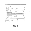
- FIGURE 3 is a perspective view of a sputtering apparatus using the target of Figs. 1-2 (or Fig. 4 ), according to an example embodiment of this invention.
- FIGURE 4 is a perspective view of a sputtering target according to another example embodiment of this invention.
- Figs. 1-2 illustrate an example sputtering target according to an example non-limiting embodiment of this invention, with Fig. 2 being a cross-sectional view of a part of the target of Fig. 1 .
- the illustrated cylindrical rotating target 1 includes a cathode tube 2 with a slow sputtering material 3 applied thereto prior to application of the target material 4 to be sputtered onto the substrate.
- the slow sputtering material 3 is on the tube 2, and is located between the cathode tube 2 and the target material 4 to be sputtered. Both the slow sputtering material 3 and the material 4 to be sputtered are on and supported by the cathode tube 2.
- Materials 3 and 4 may be formed on the tube 2 in any suitable manner (e.g., via plasma spraying).
- the use of the slow sputtering material 3 between the cathode tube 2 and the material 4 to be sputtered is advantageous in that this can reduce the risk of bum-through to, or of, the tube 2 during sputtering (e.g., especially in or near the turn-around area of the target).
- the target's lifetime and/or utilization may also be increased through the use of the slow sputtering material.
- Example slow-sputtering materials that may be used for layer 3 include Ti, W, Nb, Ta, and so forth.
- Example target materials that may be used for target material layer 4 include, Sn, Zn and the like.
- the slow sputtering material has both mechanical durability and good adhesion to both the cathode tube and the sputtering/target material.
- the material of target material layer 4 has a faster sputtering rate than does the material of layer 3 in certain example embodiments of this invention.
- Layers 3 and 4 are both conductive in certain example embodiments of this invention. However, ceramic material may be used for layer 3 and/or layer 4.
- magnet array 5 which is typically stationary even when the tube 2 (and layers 3, 4 thereon) is rotating, inside the tube causes the target material to be sputtered unevenly in certain areas. This can result in burn-through, for example in an area where the sputtering rate of the target material is unusually fast.
- material 3 is designed to prevent or reduce the likelihood of such burn-through.
- Hollow cathode tubes 2 are generally made of stainless steel. Burning through a target material 4 would sputter material from the backing tube 2, resulting in contamination of the sputtered film being deposited on the substrate. If allowed to continue, a hole could develop in the backing tube 2 which would allow cooling water to enter the chamber; this would damage the product being made and/or sputtering apparatus.
- the slow sputter material layer 3 has a thickness of 1-8 mm to provide integrity. The thickness of the target material layer 4 is from 6 to 16 mm.
- the cathode tube would not be made of stainless steel, but instead would be made of a slow sputter material such as Ti, W, Nb, Ta, or the like.
- target materials 4 to be sputtered e.g., Sn, Zn, etc.
- the slow sputtering material can protect the target tube from burn-through.
- the slow sputtering material may extend along the entire, or substantially the entire, length of the target tube 2, and/or is not exposed during normal sputtering operations.
- Fig. 4 illustrates a sputtering target according to another example embodiment of this invention.
- a layer or coating 8 of non-conductive material e.g., an oxide of Si, Sn, Zn, etc.
- the dielectric material 8 may be applied to substantially only the dogbone section, or alternatively along the entire tube length since there is no conductivity requirement for the target material.
- This non-conductive material 8 is provided between the cathode tube 2 and the target material 4, and is used to protect against burn-through.
- Non-conductive material 8 located in the racetrack or dogbone section of the target near the end(s) thereof, is effective in that the etching pattern (sputtering) will slow down or substantially stop at the non-conductive material 8 when the target material 4 in that area has been consumed (sputtered off ) since the surface charge will prevent or substantially reduce sputtering ion (e.g., Ar+) bombardment. This is also advantageous in that it will reduce contamination of the film being sputtered onto the substrate.
- non-conductive 8 material under a conductive target material could cause an increase in micro-arcing (not big hard arcs) when the non-conductive material is exposed during sputtering, this micro-arcing should not significantly affect coating the product but instead could be advantageous in that it can give an operator a signal or indication as to how much of the target life is left (e.g., it is time to replace the target, or soon will be).
- Fig. 3 is a cross sectional view of a sputtering apparatus that can use the target 1 of Figs. 1-2 or 4 .
- the sputtering apparatus includes cooling tubes 11, 12 through which cooling fluid (e.g., water) flows in order to cool the target and/or magnets during sputtering operations.
- the target 1 is rotatably mounted to support 14 so that during sputtering operations the target 1 rotates relative to the support 14. Shields (not shown) may also be provided in a known manner.
Landscapes
- Chemical & Material Sciences (AREA)
- Engineering & Computer Science (AREA)
- Physics & Mathematics (AREA)
- Plasma & Fusion (AREA)
- Analytical Chemistry (AREA)
- Chemical Kinetics & Catalysis (AREA)
- Materials Engineering (AREA)
- Mechanical Engineering (AREA)
- Metallurgy (AREA)
- Organic Chemistry (AREA)
- Physical Vapour Deposition (AREA)
Priority Applications (1)
| Application Number | Priority Date | Filing Date | Title |
|---|---|---|---|
| PL06785376T PL1913624T3 (pl) | 2005-06-22 | 2006-06-21 | Tarcza do rozpylania z powolnie rozpylaną warstwą pod materiałem tarczy |
Applications Claiming Priority (2)
| Application Number | Priority Date | Filing Date | Title |
|---|---|---|---|
| US11/158,407 US20060289304A1 (en) | 2005-06-22 | 2005-06-22 | Sputtering target with slow-sputter layer under target material |
| PCT/US2006/024371 WO2007002330A1 (en) | 2005-06-22 | 2006-06-21 | Sputtering target with slow-sputter layer under target material |
Publications (2)
| Publication Number | Publication Date |
|---|---|
| EP1913624A1 EP1913624A1 (en) | 2008-04-23 |
| EP1913624B1 true EP1913624B1 (en) | 2011-08-10 |
Family
ID=37311923
Family Applications (1)
| Application Number | Title | Priority Date | Filing Date |
|---|---|---|---|
| EP06785376A Not-in-force EP1913624B1 (en) | 2005-06-22 | 2006-06-21 | Sputtering target with slow-sputter layer under target material |
Country Status (7)
| Country | Link |
|---|---|
| US (1) | US20060289304A1 (pl) |
| EP (1) | EP1913624B1 (pl) |
| AT (1) | ATE520143T1 (pl) |
| CA (1) | CA2611345A1 (pl) |
| ES (1) | ES2370259T3 (pl) |
| PL (1) | PL1913624T3 (pl) |
| WO (1) | WO2007002330A1 (pl) |
Cited By (5)
| Publication number | Priority date | Publication date | Assignee | Title |
|---|---|---|---|---|
| US20140216343A1 (en) | 2008-08-04 | 2014-08-07 | Agc Flat Glass North America, Inc. | Plasma source and methods for depositing thin film coatings using plasma enhanced chemical vapor deposition |
| US9721764B2 (en) | 2015-11-16 | 2017-08-01 | Agc Flat Glass North America, Inc. | Method of producing plasma by multiple-phase alternating or pulsed electrical current |
| US9721765B2 (en) | 2015-11-16 | 2017-08-01 | Agc Flat Glass North America, Inc. | Plasma device driven by multiple-phase alternating or pulsed electrical current |
| US10242846B2 (en) | 2015-12-18 | 2019-03-26 | Agc Flat Glass North America, Inc. | Hollow cathode ion source |
| US10573499B2 (en) | 2015-12-18 | 2020-02-25 | Agc Flat Glass North America, Inc. | Method of extracting and accelerating ions |
Families Citing this family (10)
| Publication number | Priority date | Publication date | Assignee | Title |
|---|---|---|---|---|
| GB0713450D0 (en) * | 2007-07-12 | 2007-08-22 | Materia Nova | Magnetron co-sputtering device |
| GB2461094B (en) * | 2008-06-20 | 2012-08-22 | Mantis Deposition Ltd | Deposition of materials |
| US20100025229A1 (en) * | 2008-07-30 | 2010-02-04 | Guardian Industries Corp. | Apparatus and method for sputtering target debris reduction |
| US20100044222A1 (en) * | 2008-08-21 | 2010-02-25 | Guardian Industries Corp., | Sputtering target including magnetic field uniformity enhancing sputtering target backing tube |
| DE102010038796B4 (de) * | 2010-08-02 | 2014-02-20 | Von Ardenne Anlagentechnik Gmbh | Dünnschichtsolarzelle und Verfahren zu ihrer Herstellung |
| JP6037734B2 (ja) * | 2012-09-07 | 2016-12-07 | 三菱重工工作機械株式会社 | 常温接合装置および常温接合方法 |
| KR102177208B1 (ko) * | 2013-07-25 | 2020-11-11 | 삼성디스플레이 주식회사 | 스퍼터링 시스템과, 이를 이용한 디스플레이 장치의 제조 방법 |
| KR102272311B1 (ko) | 2014-12-05 | 2021-07-06 | 에이쥐씨 글래스 유럽 | 중공형 음극 플라즈마 소스 |
| ES2900321T3 (es) | 2014-12-05 | 2022-03-16 | Agc Flat Glass Na Inc | Fuente de plasma que utiliza un recubrimiento de reducción de macropartículas y procedimiento para usar una fuente de plasma que utiliza un recubrimiento de reducción de macropartículas para la deposición de recubrimientos de película delgada y modificación de superficies |
| CN113001114B (zh) * | 2021-03-01 | 2023-12-29 | 宁波江丰电子材料股份有限公司 | 一种旋转靶材溅射面的车削方法 |
Family Cites Families (18)
| Publication number | Priority date | Publication date | Assignee | Title |
|---|---|---|---|---|
| DE2933835C2 (de) * | 1979-08-21 | 1987-02-19 | Siemens AG, 1000 Berlin und 8000 München | Verfahren zum Befestigen von in Scheiben- oder Plattenform vorliegenden Targetmaterialien auf Kühlteller für Aufstäubanlagen |
| US4356073A (en) * | 1981-02-12 | 1982-10-26 | Shatterproof Glass Corporation | Magnetron cathode sputtering apparatus |
| US5354446A (en) * | 1988-03-03 | 1994-10-11 | Asahi Glass Company Ltd. | Ceramic rotatable magnetron sputtering cathode target and process for its production |
| US5427665A (en) * | 1990-07-11 | 1995-06-27 | Leybold Aktiengesellschaft | Process and apparatus for reactive coating of a substrate |
| JP3516949B2 (ja) * | 1990-08-10 | 2004-04-05 | バイラテック・シン・フィルムズ・インコーポレイテッド | 回転マグネトロンスパッタリングシステムにおけるアーク抑制のためのシールディング |
| US5364518A (en) * | 1991-05-28 | 1994-11-15 | Leybold Aktiengesellschaft | Magnetron cathode for a rotating target |
| JPH0586462A (ja) * | 1991-06-28 | 1993-04-06 | Mitsubishi Materials Corp | スパツタリング用ターゲツト及びその製造方法 |
| EP1452622A3 (en) * | 1995-08-23 | 2004-09-29 | Asahi Glass Ceramics Co., Ltd. | Target and process for its production, and method for forming a film having a high refractive index |
| JPH1129858A (ja) * | 1997-07-14 | 1999-02-02 | Mitsubishi Chem Corp | スパッタリングターゲット |
| DE60023176T2 (de) * | 1999-12-03 | 2006-06-14 | Bekaert Sa Nv | Sputtertarget und verfahren zur herstellung eines solchen targets |
| KR20030024868A (ko) * | 2000-08-17 | 2003-03-26 | 토소우 에스엠디, 인크 | 수명-종료-표시를 갖는 고순도 스퍼터 타켓과 이의 제조방법 |
| EP1321537A4 (en) | 2000-09-08 | 2006-06-07 | Asahi Glass Co Ltd | CYLINDRICAL TARGET AND MANUFACTURING METHOD FOR CYLINDRICAL TARGET |
| AU9304201A (en) | 2000-09-25 | 2002-04-08 | Cardinal Cg Co | Improved sputtering target and methods of making and using same |
| US20040115362A1 (en) * | 2002-01-14 | 2004-06-17 | Klause Hartig | Photocatalytic sputtering targets and methods for the production and use thereof |
| AU2003248835A1 (en) * | 2002-07-02 | 2004-01-23 | Academy Precision Materials A Division Of Academy Corporation | Rotary target and method for onsite mechanical assembly of rotary target |
| DE60326621D1 (de) * | 2002-10-21 | 2009-04-23 | Cabot Corp | Verfahren zur herstellung eines sputtertargets und sputtertarget |
| US7014741B2 (en) * | 2003-02-21 | 2006-03-21 | Von Ardenne Anlagentechnik Gmbh | Cylindrical magnetron with self cleaning target |
| US20050051422A1 (en) * | 2003-02-21 | 2005-03-10 | Rietzel James G. | Cylindrical magnetron with self cleaning target |
-
2005
- 2005-06-22 US US11/158,407 patent/US20060289304A1/en not_active Abandoned
-
2006
- 2006-06-21 CA CA002611345A patent/CA2611345A1/en not_active Abandoned
- 2006-06-21 WO PCT/US2006/024371 patent/WO2007002330A1/en not_active Ceased
- 2006-06-21 ES ES06785376T patent/ES2370259T3/es active Active
- 2006-06-21 EP EP06785376A patent/EP1913624B1/en not_active Not-in-force
- 2006-06-21 PL PL06785376T patent/PL1913624T3/pl unknown
- 2006-06-21 AT AT06785376T patent/ATE520143T1/de not_active IP Right Cessation
Cited By (11)
| Publication number | Priority date | Publication date | Assignee | Title |
|---|---|---|---|---|
| US20140216343A1 (en) | 2008-08-04 | 2014-08-07 | Agc Flat Glass North America, Inc. | Plasma source and methods for depositing thin film coatings using plasma enhanced chemical vapor deposition |
| US20150002021A1 (en) | 2008-08-04 | 2015-01-01 | Agc Flat Glass North America, Inc. | Plasma source and methods for depositing thin film coatings using plasma enhanced chemical vapor deposition |
| US20150004330A1 (en) | 2008-08-04 | 2015-01-01 | Agc Flat Glass North America, Inc. | Plasma source and methods for depositing thin film coatings using plasma enhanced chemical vapor deposition |
| US10438778B2 (en) | 2008-08-04 | 2019-10-08 | Agc Flat Glass North America, Inc. | Plasma source and methods for depositing thin film coatings using plasma enhanced chemical vapor deposition |
| US10580624B2 (en) | 2008-08-04 | 2020-03-03 | Agc Flat Glass North America, Inc. | Plasma source and methods for depositing thin film coatings using plasma enhanced chemical vapor deposition |
| US10580625B2 (en) | 2008-08-04 | 2020-03-03 | Agc Flat Glass North America, Inc. | Plasma source and methods for depositing thin film coatings using plasma enhanced chemical vapor deposition |
| US9721764B2 (en) | 2015-11-16 | 2017-08-01 | Agc Flat Glass North America, Inc. | Method of producing plasma by multiple-phase alternating or pulsed electrical current |
| US9721765B2 (en) | 2015-11-16 | 2017-08-01 | Agc Flat Glass North America, Inc. | Plasma device driven by multiple-phase alternating or pulsed electrical current |
| US10559452B2 (en) | 2015-11-16 | 2020-02-11 | Agc Flat Glass North America, Inc. | Plasma device driven by multiple-phase alternating or pulsed electrical current |
| US10242846B2 (en) | 2015-12-18 | 2019-03-26 | Agc Flat Glass North America, Inc. | Hollow cathode ion source |
| US10573499B2 (en) | 2015-12-18 | 2020-02-25 | Agc Flat Glass North America, Inc. | Method of extracting and accelerating ions |
Also Published As
| Publication number | Publication date |
|---|---|
| CA2611345A1 (en) | 2007-01-04 |
| ATE520143T1 (de) | 2011-08-15 |
| EP1913624A1 (en) | 2008-04-23 |
| PL1913624T3 (pl) | 2012-01-31 |
| WO2007002330A1 (en) | 2007-01-04 |
| US20060289304A1 (en) | 2006-12-28 |
| ES2370259T3 (es) | 2011-12-14 |
Similar Documents
| Publication | Publication Date | Title |
|---|---|---|
| EP1913624B1 (en) | Sputtering target with slow-sputter layer under target material | |
| JP3516949B2 (ja) | 回転マグネトロンスパッタリングシステムにおけるアーク抑制のためのシールディング | |
| EP1926839B1 (en) | Sputtering target with bonding layer of varying thickness under target material | |
| US20070012558A1 (en) | Magnetron sputtering system for large-area substrates | |
| CN104024471B (zh) | 溅射装置 | |
| WO2004010455A2 (en) | Ion beam source with coated electrode | |
| EP1489643A3 (en) | Method and apparatus for ionized physical vapor deposition | |
| EP0538363B1 (en) | Device for magnetron sputtering having slotted cylindrical hollow cathode | |
| EP0853330A2 (en) | Ionized PVD source to produce uniform low-particle deposition | |
| US8652310B2 (en) | Trim magnets to adjust erosion rate of cylindrical sputter targets | |
| KR20010020525A (ko) | 스퍼터 코팅 시스템 및 기판 전극을 사용하는 방법 | |
| US6475353B1 (en) | Apparatus and method for sputter depositing dielectric films on a substrate | |
| TW200415251A (en) | Target for sputtering, sputtering device, and sputtering method | |
| EP3095126A1 (en) | Endblock for rotatable target with electrical connection between collector and rotor at pressure less than atmospheric pressure | |
| JP4902051B2 (ja) | バイアススパッタリング装置 | |
| US20140110248A1 (en) | Chamber pasting method in a pvd chamber for reactive re-sputtering dielectric material | |
| JP2008007837A (ja) | スパッタ成膜装置およびスパッタ成膜方法 | |
| US20180327897A1 (en) | Re-deposition free sputtering system | |
| KR102535667B1 (ko) | 스퍼터링 디바이스, 증착 장치, 및 스퍼터링 디바이스를 작동시키는 방법 | |
| SG172389A1 (en) | Charged particle beam pvd device, shielding device, coating chamber for coating substrates, and method of coating | |
| JP2008038192A (ja) | スパッタ源、スパッタ成膜装置およびスパッタ成膜方法 | |
| JPH09111448A (ja) | スパッタ装置 | |
| JP2025076687A (ja) | 成膜装置及び成膜方法 | |
| JP2000144407A (ja) | スパッタリング装置 | |
| CN101385114A (zh) | 真空溅射系统的阴极 |
Legal Events
| Date | Code | Title | Description |
|---|---|---|---|
| PUAI | Public reference made under article 153(3) epc to a published international application that has entered the european phase |
Free format text: ORIGINAL CODE: 0009012 |
|
| 17P | Request for examination filed |
Effective date: 20080117 |
|
| AK | Designated contracting states |
Kind code of ref document: A1 Designated state(s): AT BE BG CH CY CZ DE DK EE ES FI FR GB GR HU IE IS IT LI LT LU LV MC NL PL PT RO SE SI SK TR |
|
| 17Q | First examination report despatched |
Effective date: 20080627 |
|
| DAX | Request for extension of the european patent (deleted) | ||
| GRAP | Despatch of communication of intention to grant a patent |
Free format text: ORIGINAL CODE: EPIDOSNIGR1 |
|
| GRAS | Grant fee paid |
Free format text: ORIGINAL CODE: EPIDOSNIGR3 |
|
| GRAA | (expected) grant |
Free format text: ORIGINAL CODE: 0009210 |
|
| AK | Designated contracting states |
Kind code of ref document: B1 Designated state(s): AT BE BG CH CY CZ DE DK EE ES FI FR GB GR HU IE IS IT LI LT LU LV MC NL PL PT RO SE SI SK TR |
|
| REG | Reference to a national code |
Ref country code: GB Ref legal event code: FG4D |
|
| REG | Reference to a national code |
Ref country code: CH Ref legal event code: EP |
|
| REG | Reference to a national code |
Ref country code: IE Ref legal event code: FG4D |
|
| REG | Reference to a national code |
Ref country code: DE Ref legal event code: R096 Ref document number: 602006023732 Country of ref document: DE Effective date: 20111006 |
|
| REG | Reference to a national code |
Ref country code: NL Ref legal event code: VDEP Effective date: 20110810 |
|
| REG | Reference to a national code |
Ref country code: ES Ref legal event code: FG2A Ref document number: 2370259 Country of ref document: ES Kind code of ref document: T3 Effective date: 20111214 |
|
| LTIE | Lt: invalidation of european patent or patent extension |
Effective date: 20110810 |
|
| PG25 | Lapsed in a contracting state [announced via postgrant information from national office to epo] |
Ref country code: IS Free format text: LAPSE BECAUSE OF FAILURE TO SUBMIT A TRANSLATION OF THE DESCRIPTION OR TO PAY THE FEE WITHIN THE PRESCRIBED TIME-LIMIT Effective date: 20111210 Ref country code: PT Free format text: LAPSE BECAUSE OF FAILURE TO SUBMIT A TRANSLATION OF THE DESCRIPTION OR TO PAY THE FEE WITHIN THE PRESCRIBED TIME-LIMIT Effective date: 20111212 Ref country code: FI Free format text: LAPSE BECAUSE OF FAILURE TO SUBMIT A TRANSLATION OF THE DESCRIPTION OR TO PAY THE FEE WITHIN THE PRESCRIBED TIME-LIMIT Effective date: 20110810 Ref country code: SE Free format text: LAPSE BECAUSE OF FAILURE TO SUBMIT A TRANSLATION OF THE DESCRIPTION OR TO PAY THE FEE WITHIN THE PRESCRIBED TIME-LIMIT Effective date: 20110810 Ref country code: NL Free format text: LAPSE BECAUSE OF FAILURE TO SUBMIT A TRANSLATION OF THE DESCRIPTION OR TO PAY THE FEE WITHIN THE PRESCRIBED TIME-LIMIT Effective date: 20110810 Ref country code: LT Free format text: LAPSE BECAUSE OF FAILURE TO SUBMIT A TRANSLATION OF THE DESCRIPTION OR TO PAY THE FEE WITHIN THE PRESCRIBED TIME-LIMIT Effective date: 20110810 |
|
| REG | Reference to a national code |
Ref country code: PL Ref legal event code: T3 |
|
| REG | Reference to a national code |
Ref country code: AT Ref legal event code: MK05 Ref document number: 520143 Country of ref document: AT Kind code of ref document: T Effective date: 20110810 |
|
| PG25 | Lapsed in a contracting state [announced via postgrant information from national office to epo] |
Ref country code: AT Free format text: LAPSE BECAUSE OF FAILURE TO SUBMIT A TRANSLATION OF THE DESCRIPTION OR TO PAY THE FEE WITHIN THE PRESCRIBED TIME-LIMIT Effective date: 20110810 Ref country code: LV Free format text: LAPSE BECAUSE OF FAILURE TO SUBMIT A TRANSLATION OF THE DESCRIPTION OR TO PAY THE FEE WITHIN THE PRESCRIBED TIME-LIMIT Effective date: 20110810 Ref country code: GR Free format text: LAPSE BECAUSE OF FAILURE TO SUBMIT A TRANSLATION OF THE DESCRIPTION OR TO PAY THE FEE WITHIN THE PRESCRIBED TIME-LIMIT Effective date: 20111111 Ref country code: SI Free format text: LAPSE BECAUSE OF FAILURE TO SUBMIT A TRANSLATION OF THE DESCRIPTION OR TO PAY THE FEE WITHIN THE PRESCRIBED TIME-LIMIT Effective date: 20110810 Ref country code: CY Free format text: LAPSE BECAUSE OF FAILURE TO SUBMIT A TRANSLATION OF THE DESCRIPTION OR TO PAY THE FEE WITHIN THE PRESCRIBED TIME-LIMIT Effective date: 20110810 |
|
| PG25 | Lapsed in a contracting state [announced via postgrant information from national office to epo] |
Ref country code: BE Free format text: LAPSE BECAUSE OF FAILURE TO SUBMIT A TRANSLATION OF THE DESCRIPTION OR TO PAY THE FEE WITHIN THE PRESCRIBED TIME-LIMIT Effective date: 20110810 |
|
| PG25 | Lapsed in a contracting state [announced via postgrant information from national office to epo] |
Ref country code: SK Free format text: LAPSE BECAUSE OF FAILURE TO SUBMIT A TRANSLATION OF THE DESCRIPTION OR TO PAY THE FEE WITHIN THE PRESCRIBED TIME-LIMIT Effective date: 20110810 Ref country code: CZ Free format text: LAPSE BECAUSE OF FAILURE TO SUBMIT A TRANSLATION OF THE DESCRIPTION OR TO PAY THE FEE WITHIN THE PRESCRIBED TIME-LIMIT Effective date: 20110810 |
|
| PG25 | Lapsed in a contracting state [announced via postgrant information from national office to epo] |
Ref country code: EE Free format text: LAPSE BECAUSE OF FAILURE TO SUBMIT A TRANSLATION OF THE DESCRIPTION OR TO PAY THE FEE WITHIN THE PRESCRIBED TIME-LIMIT Effective date: 20110810 Ref country code: RO Free format text: LAPSE BECAUSE OF FAILURE TO SUBMIT A TRANSLATION OF THE DESCRIPTION OR TO PAY THE FEE WITHIN THE PRESCRIBED TIME-LIMIT Effective date: 20110810 |
|
| PLBE | No opposition filed within time limit |
Free format text: ORIGINAL CODE: 0009261 |
|
| STAA | Information on the status of an ep patent application or granted ep patent |
Free format text: STATUS: NO OPPOSITION FILED WITHIN TIME LIMIT |
|
| PG25 | Lapsed in a contracting state [announced via postgrant information from national office to epo] |
Ref country code: DK Free format text: LAPSE BECAUSE OF FAILURE TO SUBMIT A TRANSLATION OF THE DESCRIPTION OR TO PAY THE FEE WITHIN THE PRESCRIBED TIME-LIMIT Effective date: 20110810 |
|
| 26N | No opposition filed |
Effective date: 20120511 |
|
| REG | Reference to a national code |
Ref country code: DE Ref legal event code: R097 Ref document number: 602006023732 Country of ref document: DE Effective date: 20120511 |
|
| PG25 | Lapsed in a contracting state [announced via postgrant information from national office to epo] |
Ref country code: MC Free format text: LAPSE BECAUSE OF NON-PAYMENT OF DUE FEES Effective date: 20120630 |
|
| REG | Reference to a national code |
Ref country code: CH Ref legal event code: PL |
|
| REG | Reference to a national code |
Ref country code: CH Ref legal event code: PL |
|
| REG | Reference to a national code |
Ref country code: IE Ref legal event code: MM4A |
|
| PG25 | Lapsed in a contracting state [announced via postgrant information from national office to epo] |
Ref country code: IE Free format text: LAPSE BECAUSE OF NON-PAYMENT OF DUE FEES Effective date: 20120621 Ref country code: CH Free format text: LAPSE BECAUSE OF NON-PAYMENT OF DUE FEES Effective date: 20120630 Ref country code: LI Free format text: LAPSE BECAUSE OF NON-PAYMENT OF DUE FEES Effective date: 20120630 |
|
| PG25 | Lapsed in a contracting state [announced via postgrant information from national office to epo] |
Ref country code: BG Free format text: LAPSE BECAUSE OF FAILURE TO SUBMIT A TRANSLATION OF THE DESCRIPTION OR TO PAY THE FEE WITHIN THE PRESCRIBED TIME-LIMIT Effective date: 20111110 |
|
| PG25 | Lapsed in a contracting state [announced via postgrant information from national office to epo] |
Ref country code: TR Free format text: LAPSE BECAUSE OF FAILURE TO SUBMIT A TRANSLATION OF THE DESCRIPTION OR TO PAY THE FEE WITHIN THE PRESCRIBED TIME-LIMIT Effective date: 20110810 |
|
| PG25 | Lapsed in a contracting state [announced via postgrant information from national office to epo] |
Ref country code: LU Free format text: LAPSE BECAUSE OF NON-PAYMENT OF DUE FEES Effective date: 20120621 |
|
| PG25 | Lapsed in a contracting state [announced via postgrant information from national office to epo] |
Ref country code: HU Free format text: LAPSE BECAUSE OF FAILURE TO SUBMIT A TRANSLATION OF THE DESCRIPTION OR TO PAY THE FEE WITHIN THE PRESCRIBED TIME-LIMIT Effective date: 20060621 |
|
| REG | Reference to a national code |
Ref country code: FR Ref legal event code: PLFP Year of fee payment: 11 |
|
| REG | Reference to a national code |
Ref country code: FR Ref legal event code: PLFP Year of fee payment: 12 |
|
| REG | Reference to a national code |
Ref country code: FR Ref legal event code: PLFP Year of fee payment: 13 |
|
| REG | Reference to a national code |
Ref country code: DE Ref legal event code: R082 Ref document number: 602006023732 Country of ref document: DE Representative=s name: HOYNG ROKH MONEGIER LLP, NL Ref country code: DE Ref legal event code: R082 Ref document number: 602006023732 Country of ref document: DE Representative=s name: HOYNG ROKH MONEGIER B.V., NL |
|
| PGFP | Annual fee paid to national office [announced via postgrant information from national office to epo] |
Ref country code: DE Payment date: 20190612 Year of fee payment: 14 Ref country code: PL Payment date: 20190416 Year of fee payment: 14 Ref country code: IT Payment date: 20190620 Year of fee payment: 14 |
|
| PGFP | Annual fee paid to national office [announced via postgrant information from national office to epo] |
Ref country code: FR Payment date: 20190510 Year of fee payment: 14 |
|
| PGFP | Annual fee paid to national office [announced via postgrant information from national office to epo] |
Ref country code: ES Payment date: 20190701 Year of fee payment: 14 Ref country code: GB Payment date: 20190619 Year of fee payment: 14 |
|
| REG | Reference to a national code |
Ref country code: GB Ref legal event code: 732E Free format text: REGISTERED BETWEEN 20200709 AND 20200715 |
|
| REG | Reference to a national code |
Ref country code: DE Ref legal event code: R119 Ref document number: 602006023732 Country of ref document: DE |
|
| GBPC | Gb: european patent ceased through non-payment of renewal fee |
Effective date: 20200621 |
|
| PG25 | Lapsed in a contracting state [announced via postgrant information from national office to epo] |
Ref country code: FR Free format text: LAPSE BECAUSE OF NON-PAYMENT OF DUE FEES Effective date: 20200630 Ref country code: GB Free format text: LAPSE BECAUSE OF NON-PAYMENT OF DUE FEES Effective date: 20200621 |
|
| PG25 | Lapsed in a contracting state [announced via postgrant information from national office to epo] |
Ref country code: DE Free format text: LAPSE BECAUSE OF NON-PAYMENT OF DUE FEES Effective date: 20210101 |
|
| PG25 | Lapsed in a contracting state [announced via postgrant information from national office to epo] |
Ref country code: IT Free format text: LAPSE BECAUSE OF NON-PAYMENT OF DUE FEES Effective date: 20200621 |
|
| REG | Reference to a national code |
Ref country code: ES Ref legal event code: FD2A Effective date: 20211126 |
|
| PG25 | Lapsed in a contracting state [announced via postgrant information from national office to epo] |
Ref country code: ES Free format text: LAPSE BECAUSE OF NON-PAYMENT OF DUE FEES Effective date: 20200622 |
|
| PG25 | Lapsed in a contracting state [announced via postgrant information from national office to epo] |
Ref country code: PL Free format text: LAPSE BECAUSE OF NON-PAYMENT OF DUE FEES Effective date: 20200621 |