EP1912095B1 - Display panel manufacture - Google Patents
Display panel manufacture Download PDFInfo
- Publication number
- EP1912095B1 EP1912095B1 EP07019888A EP07019888A EP1912095B1 EP 1912095 B1 EP1912095 B1 EP 1912095B1 EP 07019888 A EP07019888 A EP 07019888A EP 07019888 A EP07019888 A EP 07019888A EP 1912095 B1 EP1912095 B1 EP 1912095B1
- Authority
- EP
- European Patent Office
- Prior art keywords
- electrode
- color filter
- display panel
- pixel
- insulating layer
- Prior art date
- Legal status (The legal status is an assumption and is not a legal conclusion. Google has not performed a legal analysis and makes no representation as to the accuracy of the status listed.)
- Active
Links
Images


Classifications
-
- G—PHYSICS
- G02—OPTICS
- G02F—OPTICAL DEVICES OR ARRANGEMENTS FOR THE CONTROL OF LIGHT BY MODIFICATION OF THE OPTICAL PROPERTIES OF THE MEDIA OF THE ELEMENTS INVOLVED THEREIN; NON-LINEAR OPTICS; FREQUENCY-CHANGING OF LIGHT; OPTICAL LOGIC ELEMENTS; OPTICAL ANALOGUE/DIGITAL CONVERTERS
- G02F1/00—Devices or arrangements for the control of the intensity, colour, phase, polarisation or direction of light arriving from an independent light source, e.g. switching, gating or modulating; Non-linear optics
- G02F1/01—Devices or arrangements for the control of the intensity, colour, phase, polarisation or direction of light arriving from an independent light source, e.g. switching, gating or modulating; Non-linear optics for the control of the intensity, phase, polarisation or colour
- G02F1/13—Devices or arrangements for the control of the intensity, colour, phase, polarisation or direction of light arriving from an independent light source, e.g. switching, gating or modulating; Non-linear optics for the control of the intensity, phase, polarisation or colour based on liquid crystals, e.g. single liquid crystal display cells
- G02F1/133—Constructional arrangements; Operation of liquid crystal cells; Circuit arrangements
- G02F1/136—Liquid crystal cells structurally associated with a semi-conducting layer or substrate, e.g. cells forming part of an integrated circuit
- G02F1/1362—Active matrix addressed cells
- G02F1/136213—Storage capacitors associated with the pixel electrode
-
- G—PHYSICS
- G02—OPTICS
- G02F—OPTICAL DEVICES OR ARRANGEMENTS FOR THE CONTROL OF LIGHT BY MODIFICATION OF THE OPTICAL PROPERTIES OF THE MEDIA OF THE ELEMENTS INVOLVED THEREIN; NON-LINEAR OPTICS; FREQUENCY-CHANGING OF LIGHT; OPTICAL LOGIC ELEMENTS; OPTICAL ANALOGUE/DIGITAL CONVERTERS
- G02F1/00—Devices or arrangements for the control of the intensity, colour, phase, polarisation or direction of light arriving from an independent light source, e.g. switching, gating or modulating; Non-linear optics
- G02F1/01—Devices or arrangements for the control of the intensity, colour, phase, polarisation or direction of light arriving from an independent light source, e.g. switching, gating or modulating; Non-linear optics for the control of the intensity, phase, polarisation or colour
- G02F1/13—Devices or arrangements for the control of the intensity, colour, phase, polarisation or direction of light arriving from an independent light source, e.g. switching, gating or modulating; Non-linear optics for the control of the intensity, phase, polarisation or colour based on liquid crystals, e.g. single liquid crystal display cells
- G02F1/133—Constructional arrangements; Operation of liquid crystal cells; Circuit arrangements
- G02F1/1333—Constructional arrangements; Manufacturing methods
- G02F1/1343—Electrodes
-
- G—PHYSICS
- G02—OPTICS
- G02F—OPTICAL DEVICES OR ARRANGEMENTS FOR THE CONTROL OF LIGHT BY MODIFICATION OF THE OPTICAL PROPERTIES OF THE MEDIA OF THE ELEMENTS INVOLVED THEREIN; NON-LINEAR OPTICS; FREQUENCY-CHANGING OF LIGHT; OPTICAL LOGIC ELEMENTS; OPTICAL ANALOGUE/DIGITAL CONVERTERS
- G02F1/00—Devices or arrangements for the control of the intensity, colour, phase, polarisation or direction of light arriving from an independent light source, e.g. switching, gating or modulating; Non-linear optics
- G02F1/01—Devices or arrangements for the control of the intensity, colour, phase, polarisation or direction of light arriving from an independent light source, e.g. switching, gating or modulating; Non-linear optics for the control of the intensity, phase, polarisation or colour
- G02F1/13—Devices or arrangements for the control of the intensity, colour, phase, polarisation or direction of light arriving from an independent light source, e.g. switching, gating or modulating; Non-linear optics for the control of the intensity, phase, polarisation or colour based on liquid crystals, e.g. single liquid crystal display cells
- G02F1/133—Constructional arrangements; Operation of liquid crystal cells; Circuit arrangements
- G02F1/1333—Constructional arrangements; Manufacturing methods
- G02F1/1335—Structural association of cells with optical devices, e.g. polarisers or reflectors
- G02F1/133509—Filters, e.g. light shielding masks
- G02F1/133514—Colour filters
-
- G—PHYSICS
- G02—OPTICS
- G02F—OPTICAL DEVICES OR ARRANGEMENTS FOR THE CONTROL OF LIGHT BY MODIFICATION OF THE OPTICAL PROPERTIES OF THE MEDIA OF THE ELEMENTS INVOLVED THEREIN; NON-LINEAR OPTICS; FREQUENCY-CHANGING OF LIGHT; OPTICAL LOGIC ELEMENTS; OPTICAL ANALOGUE/DIGITAL CONVERTERS
- G02F1/00—Devices or arrangements for the control of the intensity, colour, phase, polarisation or direction of light arriving from an independent light source, e.g. switching, gating or modulating; Non-linear optics
- G02F1/01—Devices or arrangements for the control of the intensity, colour, phase, polarisation or direction of light arriving from an independent light source, e.g. switching, gating or modulating; Non-linear optics for the control of the intensity, phase, polarisation or colour
- G02F1/13—Devices or arrangements for the control of the intensity, colour, phase, polarisation or direction of light arriving from an independent light source, e.g. switching, gating or modulating; Non-linear optics for the control of the intensity, phase, polarisation or colour based on liquid crystals, e.g. single liquid crystal display cells
- G02F1/133—Constructional arrangements; Operation of liquid crystal cells; Circuit arrangements
- G02F1/1333—Constructional arrangements; Manufacturing methods
- G02F1/1341—Filling or closing of cells
-
- G—PHYSICS
- G02—OPTICS
- G02F—OPTICAL DEVICES OR ARRANGEMENTS FOR THE CONTROL OF LIGHT BY MODIFICATION OF THE OPTICAL PROPERTIES OF THE MEDIA OF THE ELEMENTS INVOLVED THEREIN; NON-LINEAR OPTICS; FREQUENCY-CHANGING OF LIGHT; OPTICAL LOGIC ELEMENTS; OPTICAL ANALOGUE/DIGITAL CONVERTERS
- G02F1/00—Devices or arrangements for the control of the intensity, colour, phase, polarisation or direction of light arriving from an independent light source, e.g. switching, gating or modulating; Non-linear optics
- G02F1/01—Devices or arrangements for the control of the intensity, colour, phase, polarisation or direction of light arriving from an independent light source, e.g. switching, gating or modulating; Non-linear optics for the control of the intensity, phase, polarisation or colour
- G02F1/13—Devices or arrangements for the control of the intensity, colour, phase, polarisation or direction of light arriving from an independent light source, e.g. switching, gating or modulating; Non-linear optics for the control of the intensity, phase, polarisation or colour based on liquid crystals, e.g. single liquid crystal display cells
- G02F1/133—Constructional arrangements; Operation of liquid crystal cells; Circuit arrangements
- G02F1/1333—Constructional arrangements; Manufacturing methods
- G02F1/1343—Electrodes
- G02F1/134309—Electrodes characterised by their geometrical arrangement
- G02F1/134318—Electrodes characterised by their geometrical arrangement having a patterned common electrode
Definitions
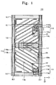
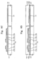
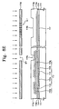
- FIG. 1 is a plan view showing a display panel according to an exemplary embodiment of the present invention.
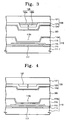
- FIG. 2 is a cross-sectional view taken along lines I-I' and II-II' of FIG. 1 .
- the first, second, and third gate lines GL1, GL2, and GL3 extend in a first direction D1, and the first and second data lines DL1 and DL2 extend in a second direction D2, which is substantially perpendicular to the first direction D1.
- the second and third gate lines GL2 and GL3 and the first and second data lines DL1 and DL2 define the rectangular-shaped pixel area PA on the first base substrate 111.
- the first and second data lines DL1 and DL2 are arranged on a different layer than the first, second, and third gate lines GL1, GL2, and GL3, so that the first and second data lines DL1 and DL2 may be electrically insulated from the first, second, and third gate lines GL1, GL2, and GL3.
- the second black matrix 126a includes the same material as that of the first black matrix 122 (shown in FIG. 2 ) and is substantially simultaneously patterned together with the first black matrix 122 through one process.
- the dummy color filter 126b has the same color as that of one color filter of color filters adjacent to the green color filter G and is substantially simultaneously patterned together with the one color filter through one process.
- the dummy color filter 126b is a red (R) color filter R.
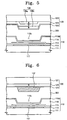
- a color filter substrate 120 includes a fourth protruding portion 128 arranged directly above the storage electrode 117, and the fourth protruding portion 128 includes a first dummy color filter 128a and a second dummy color filter 128b.
- a green color filter G is arranged on the color filter substrate 120 to cover the first dummy color filter 128a, and the second dummy color filter 128b is arranged on the green color filter G.
- a display panel 200 includes a first data line DL1, a second data line DL2, a first gate line GL1, a second gate line GL2, and a third gate line GL3.
- the first, second, and third gate lines GL1, GL2, and GL3 extend in a first direction D1
- the first and second data lines DL1 and DL2 extend in a second direction D2, which is substantially perpendicular to the first direction D1.
- a gate insulating layer 114 is formed on the first base substrate 111 to cover the first gate electrode 112a and the storage electrode 117.
- the gate insulating layer 114 may include an inorganic compound such as silicon nitride.
- An active layer 119a which includes an amorphous silicon layer, is coated on the gate insulating layer 114.
- An ohmic contact layer 119b which is doped with impurity ions, is coated on the active layer 119a.
- the gate insulating layer 114, the active layer 119a, and the ohmic contact layer 119b may be sequentially coated on an entire surface of the first base substrate 111 using a plasma chemical vapor deposition technique.
- a second photoresist pattern is formed.
- the data metal pattern and the pre-ohmic contact pattern are removed directly above the first gate metal 112a through an etching process using the second photoresist pattern as an etching mask.
- the first thin film transistor 112 is completed through the above-described processes. According to the above, the active pattern 112b, the ohmic contact pattern 112c, the first source electrode 112d, and the first drain electrode 112e are patterned using one mask, thereby simplifying the manufacturing process and reducing the manufacturing cost of a display panel.
- a first transparent insulating layer 119e and a second transparent insulating layer 119f are sequentially coated on the first thin film transistor 112 and the gate insulating layer 114.
- the second transparent insulating layer 119f includes a photosensitive acrylic resin so that the second transparent insulating layer 119f may be patterned through the photolithography process.
- the second transparent insulating layer 119f may have a negative type photoresist or a positive type photoresist.
- the second transparent insulating layer 119f including the positive type photoresist will be described as an example.
- a color filter layer 123 is formed over the second base substrate 121 to cover the first and second black matrices 122 and 125.
- the color filter layer 123 partially overlaps with the first black matrix 122 formed in a peripheral portion of the pixel area, but the color filter layer 123 covers an entire surface of the second black matrix 125 formed in the pixel area.
- the color filter layer 123 includes a red color filter, a green color filter, and a blue color filter.
- the red, green, and blue color filters may be sequentially formed through a patterning process or an inkjet printing method.
Landscapes
- Physics & Mathematics (AREA)
- Nonlinear Science (AREA)
- Mathematical Physics (AREA)
- Chemical & Material Sciences (AREA)
- Crystallography & Structural Chemistry (AREA)
- General Physics & Mathematics (AREA)
- Optics & Photonics (AREA)
- Engineering & Computer Science (AREA)
- Power Engineering (AREA)
- Microelectronics & Electronic Packaging (AREA)
- Liquid Crystal (AREA)
- Devices For Indicating Variable Information By Combining Individual Elements (AREA)
Applications Claiming Priority (1)
| Application Number | Priority Date | Filing Date | Title |
|---|---|---|---|
| KR1020060099408A KR101299646B1 (ko) | 2006-10-12 | 2006-10-12 | 표시패널 및 이의 제조방법 |
Publications (2)
| Publication Number | Publication Date |
|---|---|
| EP1912095A1 EP1912095A1 (en) | 2008-04-16 |
| EP1912095B1 true EP1912095B1 (en) | 2010-05-19 |
Family
ID=38814638
Family Applications (1)
| Application Number | Title | Priority Date | Filing Date |
|---|---|---|---|
| EP07019888A Active EP1912095B1 (en) | 2006-10-12 | 2007-10-11 | Display panel manufacture |
Country Status (6)
Families Citing this family (21)
| Publication number | Priority date | Publication date | Assignee | Title |
|---|---|---|---|---|
| KR20070075808A (ko) * | 2006-01-16 | 2007-07-24 | 삼성전자주식회사 | 표시 기판의 제조 방법 및 이를 이용하여 제조한 표시 기판 |
| TW200924107A (en) * | 2007-10-02 | 2009-06-01 | Polymer Vision Ltd | An electronic circuit element with profiled photopatternable dielectric layer |
| CN102132202A (zh) * | 2008-08-27 | 2011-07-20 | 夏普株式会社 | 有源矩阵基板、液晶面板、液晶显示装置、液晶显示单元、电视接收机 |
| BRPI0917349A2 (pt) | 2008-08-27 | 2015-11-17 | Sharp Kk | substrato de matriz ativa, painel de cristal líquido, unidade de exibição de cristal líquido, dispositivo de exibição de cristal líquido, receptor de televisão e método de fabricação de substrato de matriz ativa. |
| KR101241620B1 (ko) * | 2008-08-27 | 2013-03-11 | 샤프 가부시키가이샤 | 액티브 매트릭스 기판, 액정 패널, 액정 표시 유닛, 액정 표시 장치, 텔레비전 수상기, 액티브 매트릭스 기판의 제조 방법 |
| CN101728398A (zh) * | 2008-10-28 | 2010-06-09 | 奇美电子股份有限公司 | 薄膜晶体管基板、显示面板、显示装置及其制造方法 |
| TWI400524B (zh) * | 2008-12-02 | 2013-07-01 | Chunghwa Picture Tubes Ltd | 一種液晶顯示製程面板與形成配向膜的方法 |
| CN102375277B (zh) * | 2010-08-10 | 2014-05-28 | 乐金显示有限公司 | 液晶显示装置及其制造方法 |
| KR101778009B1 (ko) * | 2010-08-19 | 2017-09-27 | 삼성디스플레이 주식회사 | 표시 기판 및 그 제조 방법 |
| CN102566157B (zh) * | 2010-12-16 | 2014-10-08 | 京东方科技集团股份有限公司 | 阵列基板和液晶显示器 |
| KR101859483B1 (ko) * | 2012-03-06 | 2018-06-27 | 엘지디스플레이 주식회사 | 입체 영상 표시 장치 및 그 제조 방법 |
| KR101425611B1 (ko) * | 2012-07-04 | 2014-07-31 | 엘지디스플레이 주식회사 | 패턴드 리타더 방식의 입체영상 표시장치 및 그 제조 방법 |
| KR101954979B1 (ko) * | 2012-08-01 | 2019-03-08 | 삼성디스플레이 주식회사 | 컬러필터 기판과 이를 포함하는 액정 표시 장치 및 컬러필터 기판 제조 방법 |
| JP6186698B2 (ja) * | 2012-10-29 | 2017-08-30 | セイコーエプソン株式会社 | 有機el装置、電子機器 |
| US8987069B1 (en) * | 2013-12-04 | 2015-03-24 | International Business Machines Corporation | Semiconductor substrate with multiple SiGe regions having different germanium concentrations by a single epitaxy process |
| CN103728763A (zh) * | 2013-12-31 | 2014-04-16 | 深圳市华星光电技术有限公司 | 液晶面板及其制作方法 |
| KR20150086821A (ko) * | 2014-01-20 | 2015-07-29 | 삼성디스플레이 주식회사 | 액정 표시 장치 및 그 제조 방법 |
| KR102499179B1 (ko) * | 2015-09-25 | 2023-02-10 | 티씨엘 차이나 스타 옵토일렉트로닉스 테크놀로지 컴퍼니 리미티드 | 액정 표시 장치 및 그 리페어 방법 |
| CN106647059B (zh) | 2017-01-04 | 2021-01-22 | 京东方科技集团股份有限公司 | 阵列基板、显示面板及其制造方法 |
| CN108806572A (zh) * | 2017-05-05 | 2018-11-13 | 元太科技工业股份有限公司 | 像素结构 |
| CN119165685A (zh) * | 2023-06-20 | 2024-12-20 | 北京视延科技有限公司 | 显示面板及显示装置 |
Family Cites Families (13)
| Publication number | Priority date | Publication date | Assignee | Title |
|---|---|---|---|---|
| JP3014291B2 (ja) * | 1995-03-10 | 2000-02-28 | インターナショナル・ビジネス・マシーンズ・コーポレイション | 液晶表示パネル、液晶表示装置及び液晶表示パネルの製造方法 |
| JPH1096955A (ja) * | 1996-09-24 | 1998-04-14 | Toshiba Corp | 液晶表示装置 |
| CN1148600C (zh) * | 1996-11-26 | 2004-05-05 | 三星电子株式会社 | 薄膜晶体管基片及其制造方法 |
| JP2001059960A (ja) | 1999-08-23 | 2001-03-06 | Casio Comput Co Ltd | 液晶表示素子 |
| KR20020004277A (ko) * | 2000-07-04 | 2002-01-16 | 구본준, 론 위라하디락사 | 액정표시장치 |
| US7286204B2 (en) * | 2003-03-28 | 2007-10-23 | Samsung Electronics Co., Ltd. | Spacers for display devices |
| JP2004301960A (ja) * | 2003-03-28 | 2004-10-28 | Fujitsu Display Technologies Corp | 液晶表示パネル |
| KR20050000684A (ko) | 2003-06-24 | 2005-01-06 | 엘지.필립스 엘시디 주식회사 | 액정표시장치와 그 제조방법 |
| TWI261716B (en) * | 2004-05-13 | 2006-09-11 | Quanta Display Inc | Liquid crystal display apparatus and fabrication thereof |
| TWI338796B (en) * | 2004-10-29 | 2011-03-11 | Chimei Innolux Corp | Multi-domain vertically alignmentliquid crystal display panel |
| KR20060066271A (ko) * | 2004-12-13 | 2006-06-16 | 엘지.필립스 엘시디 주식회사 | 액정표시장치와 그 제조방법 |
| KR101085148B1 (ko) | 2004-12-15 | 2011-11-21 | 엘지디스플레이 주식회사 | 액정 표시 장치 및 이의 제조 방법 |
| KR20060082098A (ko) * | 2005-01-11 | 2006-07-14 | 삼성전자주식회사 | 액정 표시 장치 |
-
2006
- 2006-10-12 KR KR1020060099408A patent/KR101299646B1/ko active Active
-
2007
- 2007-10-10 JP JP2007264057A patent/JP5415687B2/ja active Active
- 2007-10-10 US US11/869,866 patent/US7742116B2/en active Active
- 2007-10-11 DE DE602007006605T patent/DE602007006605D1/de active Active
- 2007-10-11 EP EP07019888A patent/EP1912095B1/en active Active
- 2007-10-12 CN CN2007103051255A patent/CN101201521B/zh active Active
Also Published As
| Publication number | Publication date |
|---|---|
| DE602007006605D1 (de) | 2010-07-01 |
| JP5415687B2 (ja) | 2014-02-12 |
| JP2008097009A (ja) | 2008-04-24 |
| KR20080032958A (ko) | 2008-04-16 |
| US20080088788A1 (en) | 2008-04-17 |
| CN101201521B (zh) | 2011-06-01 |
| US7742116B2 (en) | 2010-06-22 |
| KR101299646B1 (ko) | 2013-08-26 |
| EP1912095A1 (en) | 2008-04-16 |
| CN101201521A (zh) | 2008-06-18 |
Similar Documents
| Publication | Publication Date | Title |
|---|---|---|
| EP1912095B1 (en) | Display panel manufacture | |
| US9570477B2 (en) | Thin film transistor array panel and manufacturing method of the same | |
| US7876412B2 (en) | Thin film transistor array panel and method for manufacturing the same | |
| US8917371B2 (en) | Liquid crystal display comprising two pixel regions juxtaposed along a signal line and separated by a gap wherein a pixel electrode is formed in one pixel region and a common electrode is formed in the other pixel region | |
| US8018540B2 (en) | Liquid crystal display and method for manufacturing the same | |
| US20080123007A1 (en) | Thin film transistor liquid crystal display | |
| US20080117150A1 (en) | Liquid crystal display and thin film transistor array panel therefor | |
| US8300192B2 (en) | Liquid crystal display and thin film transistor array panel usable with the liquid crystal display | |
| US20070141481A1 (en) | Photo Mask and method of Fabricating array Substrate for Liquid Crystal Display Device Using The Same | |
| JP2004348130A (ja) | 薄膜トランジスタ表示板及びこれを含む液晶表示装置 | |
| JP2000187209A (ja) | 反射型液晶表示装置およびその製造方法 | |
| US20100123137A1 (en) | Array substrate and method of manufacturing the same | |
| US7259807B2 (en) | Method of manufacturing thin film transistor array panel and liquid crystal display | |
| US7683371B2 (en) | Display panel and method for manufacturing the same | |
| JP2000098367A (ja) | 液晶表示装置およびその製造方法 | |
| US20080149933A1 (en) | Display panel | |
| KR101018756B1 (ko) | 액정 표시 장치 | |
| KR100992121B1 (ko) | 박막 트랜지스터 표시판 및 이를 포함하는 액정 표시 장치 | |
| KR20080100641A (ko) | 액정 표시 장치 및 이의 제조 방법 | |
| KR20060082315A (ko) | 박막 트랜지스터 표시판 | |
| KR20070044597A (ko) | 표시판 및 그 제조 방법 |
Legal Events
| Date | Code | Title | Description |
|---|---|---|---|
| PUAI | Public reference made under article 153(3) epc to a published international application that has entered the european phase |
Free format text: ORIGINAL CODE: 0009012 |
|
| AK | Designated contracting states |
Kind code of ref document: A1 Designated state(s): AT BE BG CH CY CZ DE DK EE ES FI FR GB GR HU IE IS IT LI LT LU LV MC MT NL PL PT RO SE SI SK TR |
|
| AX | Request for extension of the european patent |
Extension state: AL BA HR MK RS |
|
| 17P | Request for examination filed |
Effective date: 20081013 |
|
| 17Q | First examination report despatched |
Effective date: 20081114 |
|
| AKX | Designation fees paid |
Designated state(s): DE FR GB NL |
|
| RIN1 | Information on inventor provided before grant (corrected) |
Inventor name: MAENG, CHEON-JAE Inventor name: LEE, YUN-SEOK Inventor name: CHO, YOUNG-JE Inventor name: KIM, BYUNG-HYUN |
|
| GRAP | Despatch of communication of intention to grant a patent |
Free format text: ORIGINAL CODE: EPIDOSNIGR1 |
|
| GRAS | Grant fee paid |
Free format text: ORIGINAL CODE: EPIDOSNIGR3 |
|
| GRAA | (expected) grant |
Free format text: ORIGINAL CODE: 0009210 |
|
| AK | Designated contracting states |
Kind code of ref document: B1 Designated state(s): DE FR GB NL |
|
| REG | Reference to a national code |
Ref country code: GB Ref legal event code: FG4D |
|
| REF | Corresponds to: |
Ref document number: 602007006605 Country of ref document: DE Date of ref document: 20100701 Kind code of ref document: P |
|
| REG | Reference to a national code |
Ref country code: NL Ref legal event code: T3 |
|
| PLBE | No opposition filed within time limit |
Free format text: ORIGINAL CODE: 0009261 |
|
| STAA | Information on the status of an ep patent application or granted ep patent |
Free format text: STATUS: NO OPPOSITION FILED WITHIN TIME LIMIT |
|
| 26N | No opposition filed |
Effective date: 20110222 |
|
| REG | Reference to a national code |
Ref country code: DE Ref legal event code: R097 Ref document number: 602007006605 Country of ref document: DE Effective date: 20110221 |
|
| REG | Reference to a national code |
Ref country code: NL Ref legal event code: SD Effective date: 20121017 |
|
| REG | Reference to a national code |
Ref country code: FR Ref legal event code: TP Owner name: SAMSUNG DISPLAY CO. LTD, KR Effective date: 20130226 |
|
| REG | Reference to a national code |
Ref country code: GB Ref legal event code: 732E Free format text: REGISTERED BETWEEN 20130307 AND 20130313 |
|
| REG | Reference to a national code |
Ref country code: DE Ref legal event code: R082 Ref document number: 602007006605 Country of ref document: DE Representative=s name: DR. WEITZEL & PARTNER, DE |
|
| REG | Reference to a national code |
Ref country code: DE Ref legal event code: R081 Ref document number: 602007006605 Country of ref document: DE Owner name: SAMSUNG DISPLAY CO., LTD., KR Free format text: FORMER OWNER: SAMSUNG ELECTRONICS CO., LTD., SUWON-SI, KR Effective date: 20130422 Ref country code: DE Ref legal event code: R082 Ref document number: 602007006605 Country of ref document: DE Representative=s name: DR. WEITZEL & PARTNER, DE Effective date: 20130422 Ref country code: DE Ref legal event code: R081 Ref document number: 602007006605 Country of ref document: DE Owner name: SAMSUNG DISPLAY CO., LTD., YONGIN-CITY, KR Free format text: FORMER OWNER: SAMSUNG ELECTRONICS CO., LTD., SUWON-SI, GYEONGGI-DO, KR Effective date: 20130422 Ref country code: DE Ref legal event code: R082 Ref document number: 602007006605 Country of ref document: DE Representative=s name: DR. WEITZEL & PARTNER PATENT- UND RECHTSANWAEL, DE Effective date: 20130422 |
|
| REG | Reference to a national code |
Ref country code: FR Ref legal event code: PLFP Year of fee payment: 9 |
|
| REG | Reference to a national code |
Ref country code: FR Ref legal event code: PLFP Year of fee payment: 10 |
|
| REG | Reference to a national code |
Ref country code: FR Ref legal event code: PLFP Year of fee payment: 11 |
|
| REG | Reference to a national code |
Ref country code: FR Ref legal event code: PLFP Year of fee payment: 12 |
|
| P01 | Opt-out of the competence of the unified patent court (upc) registered |
Effective date: 20230515 |
|
| PGFP | Annual fee paid to national office [announced via postgrant information from national office to epo] |
Ref country code: GB Payment date: 20240920 Year of fee payment: 18 |
|
| PGFP | Annual fee paid to national office [announced via postgrant information from national office to epo] |
Ref country code: FR Payment date: 20240925 Year of fee payment: 18 |
|
| PGFP | Annual fee paid to national office [announced via postgrant information from national office to epo] |
Ref country code: NL Payment date: 20240920 Year of fee payment: 18 |
|
| PGFP | Annual fee paid to national office [announced via postgrant information from national office to epo] |
Ref country code: DE Payment date: 20240920 Year of fee payment: 18 |