EP1912095B1 - Display panel manufacture - Google Patents
Display panel manufacture Download PDFInfo
- Publication number
- EP1912095B1 EP1912095B1 EP07019888A EP07019888A EP1912095B1 EP 1912095 B1 EP1912095 B1 EP 1912095B1 EP 07019888 A EP07019888 A EP 07019888A EP 07019888 A EP07019888 A EP 07019888A EP 1912095 B1 EP1912095 B1 EP 1912095B1
- Authority
- EP
- European Patent Office
- Prior art keywords
- electrode
- color filter
- display panel
- pixel
- insulating layer
- Prior art date
- Legal status (The legal status is an assumption and is not a legal conclusion. Google has not performed a legal analysis and makes no representation as to the accuracy of the status listed.)
- Active
Links
- 238000004519 manufacturing process Methods 0.000 title claims description 14
- 239000000758 substrate Substances 0.000 claims description 106
- 238000003860 storage Methods 0.000 claims description 71
- 239000011159 matrix material Substances 0.000 claims description 47
- 239000010409 thin film Substances 0.000 claims description 39
- 239000004973 liquid crystal related substance Substances 0.000 claims description 34
- 238000000034 method Methods 0.000 claims description 34
- 125000006850 spacer group Chemical group 0.000 claims description 23
- 238000002161 passivation Methods 0.000 claims description 9
- 239000000463 material Substances 0.000 claims description 7
- 230000000903 blocking effect Effects 0.000 claims description 5
- 238000000059 patterning Methods 0.000 claims description 5
- 230000002093 peripheral effect Effects 0.000 claims description 5
- 239000011248 coating agent Substances 0.000 claims description 2
- 238000000576 coating method Methods 0.000 claims description 2
- 241000206607 Porphyra umbilicalis Species 0.000 claims 2
- 239000003086 colorant Substances 0.000 claims 1
- 230000008878 coupling Effects 0.000 claims 1
- 238000010168 coupling process Methods 0.000 claims 1
- 238000005859 coupling reaction Methods 0.000 claims 1
- 229910052751 metal Inorganic materials 0.000 description 13
- 239000002184 metal Substances 0.000 description 13
- 229920002120 photoresistant polymer Polymers 0.000 description 13
- 238000005530 etching Methods 0.000 description 9
- 239000003990 capacitor Substances 0.000 description 8
- 239000011651 chromium Substances 0.000 description 4
- 230000003247 decreasing effect Effects 0.000 description 3
- VYZAMTAEIAYCRO-UHFFFAOYSA-N Chromium Chemical compound [Cr] VYZAMTAEIAYCRO-UHFFFAOYSA-N 0.000 description 2
- 229910052804 chromium Inorganic materials 0.000 description 2
- 239000010949 copper Substances 0.000 description 2
- 238000012986 modification Methods 0.000 description 2
- 230000004048 modification Effects 0.000 description 2
- 238000000206 photolithography Methods 0.000 description 2
- 239000000126 substance Substances 0.000 description 2
- 239000004925 Acrylic resin Substances 0.000 description 1
- 229920000178 Acrylic resin Polymers 0.000 description 1
- RYGMFSIKBFXOCR-UHFFFAOYSA-N Copper Chemical compound [Cu] RYGMFSIKBFXOCR-UHFFFAOYSA-N 0.000 description 1
- 229910052581 Si3N4 Inorganic materials 0.000 description 1
- BQCADISMDOOEFD-UHFFFAOYSA-N Silver Chemical compound [Ag] BQCADISMDOOEFD-UHFFFAOYSA-N 0.000 description 1
- 229910052782 aluminium Inorganic materials 0.000 description 1
- XAGFODPZIPBFFR-UHFFFAOYSA-N aluminium Chemical compound [Al] XAGFODPZIPBFFR-UHFFFAOYSA-N 0.000 description 1
- 229910021417 amorphous silicon Inorganic materials 0.000 description 1
- 238000005229 chemical vapour deposition Methods 0.000 description 1
- 229910052802 copper Inorganic materials 0.000 description 1
- 239000012535 impurity Substances 0.000 description 1
- 238000007641 inkjet printing Methods 0.000 description 1
- 150000002484 inorganic compounds Chemical class 0.000 description 1
- 229910010272 inorganic material Inorganic materials 0.000 description 1
- 150000002500 ions Chemical class 0.000 description 1
- 229910001092 metal group alloy Inorganic materials 0.000 description 1
- 239000007769 metal material Substances 0.000 description 1
- 239000011368 organic material Substances 0.000 description 1
- HQVNEWCFYHHQES-UHFFFAOYSA-N silicon nitride Chemical compound N12[Si]34N5[Si]62N3[Si]51N64 HQVNEWCFYHHQES-UHFFFAOYSA-N 0.000 description 1
- 229910052709 silver Inorganic materials 0.000 description 1
- 239000004332 silver Substances 0.000 description 1
- 238000001039 wet etching Methods 0.000 description 1
Images


Classifications
-
- G—PHYSICS
- G02—OPTICS
- G02F—OPTICAL DEVICES OR ARRANGEMENTS FOR THE CONTROL OF LIGHT BY MODIFICATION OF THE OPTICAL PROPERTIES OF THE MEDIA OF THE ELEMENTS INVOLVED THEREIN; NON-LINEAR OPTICS; FREQUENCY-CHANGING OF LIGHT; OPTICAL LOGIC ELEMENTS; OPTICAL ANALOGUE/DIGITAL CONVERTERS
- G02F1/00—Devices or arrangements for the control of the intensity, colour, phase, polarisation or direction of light arriving from an independent light source, e.g. switching, gating or modulating; Non-linear optics
- G02F1/01—Devices or arrangements for the control of the intensity, colour, phase, polarisation or direction of light arriving from an independent light source, e.g. switching, gating or modulating; Non-linear optics for the control of the intensity, phase, polarisation or colour
- G02F1/13—Devices or arrangements for the control of the intensity, colour, phase, polarisation or direction of light arriving from an independent light source, e.g. switching, gating or modulating; Non-linear optics for the control of the intensity, phase, polarisation or colour based on liquid crystals, e.g. single liquid crystal display cells
- G02F1/133—Constructional arrangements; Operation of liquid crystal cells; Circuit arrangements
- G02F1/136—Liquid crystal cells structurally associated with a semi-conducting layer or substrate, e.g. cells forming part of an integrated circuit
- G02F1/1362—Active matrix addressed cells
- G02F1/136213—Storage capacitors associated with the pixel electrode
-
- G—PHYSICS
- G02—OPTICS
- G02F—OPTICAL DEVICES OR ARRANGEMENTS FOR THE CONTROL OF LIGHT BY MODIFICATION OF THE OPTICAL PROPERTIES OF THE MEDIA OF THE ELEMENTS INVOLVED THEREIN; NON-LINEAR OPTICS; FREQUENCY-CHANGING OF LIGHT; OPTICAL LOGIC ELEMENTS; OPTICAL ANALOGUE/DIGITAL CONVERTERS
- G02F1/00—Devices or arrangements for the control of the intensity, colour, phase, polarisation or direction of light arriving from an independent light source, e.g. switching, gating or modulating; Non-linear optics
- G02F1/01—Devices or arrangements for the control of the intensity, colour, phase, polarisation or direction of light arriving from an independent light source, e.g. switching, gating or modulating; Non-linear optics for the control of the intensity, phase, polarisation or colour
- G02F1/13—Devices or arrangements for the control of the intensity, colour, phase, polarisation or direction of light arriving from an independent light source, e.g. switching, gating or modulating; Non-linear optics for the control of the intensity, phase, polarisation or colour based on liquid crystals, e.g. single liquid crystal display cells
- G02F1/133—Constructional arrangements; Operation of liquid crystal cells; Circuit arrangements
- G02F1/1333—Constructional arrangements; Manufacturing methods
- G02F1/1343—Electrodes
-
- G—PHYSICS
- G02—OPTICS
- G02F—OPTICAL DEVICES OR ARRANGEMENTS FOR THE CONTROL OF LIGHT BY MODIFICATION OF THE OPTICAL PROPERTIES OF THE MEDIA OF THE ELEMENTS INVOLVED THEREIN; NON-LINEAR OPTICS; FREQUENCY-CHANGING OF LIGHT; OPTICAL LOGIC ELEMENTS; OPTICAL ANALOGUE/DIGITAL CONVERTERS
- G02F1/00—Devices or arrangements for the control of the intensity, colour, phase, polarisation or direction of light arriving from an independent light source, e.g. switching, gating or modulating; Non-linear optics
- G02F1/01—Devices or arrangements for the control of the intensity, colour, phase, polarisation or direction of light arriving from an independent light source, e.g. switching, gating or modulating; Non-linear optics for the control of the intensity, phase, polarisation or colour
- G02F1/13—Devices or arrangements for the control of the intensity, colour, phase, polarisation or direction of light arriving from an independent light source, e.g. switching, gating or modulating; Non-linear optics for the control of the intensity, phase, polarisation or colour based on liquid crystals, e.g. single liquid crystal display cells
- G02F1/133—Constructional arrangements; Operation of liquid crystal cells; Circuit arrangements
- G02F1/1333—Constructional arrangements; Manufacturing methods
- G02F1/1335—Structural association of cells with optical devices, e.g. polarisers or reflectors
- G02F1/133509—Filters, e.g. light shielding masks
- G02F1/133514—Colour filters
-
- G—PHYSICS
- G02—OPTICS
- G02F—OPTICAL DEVICES OR ARRANGEMENTS FOR THE CONTROL OF LIGHT BY MODIFICATION OF THE OPTICAL PROPERTIES OF THE MEDIA OF THE ELEMENTS INVOLVED THEREIN; NON-LINEAR OPTICS; FREQUENCY-CHANGING OF LIGHT; OPTICAL LOGIC ELEMENTS; OPTICAL ANALOGUE/DIGITAL CONVERTERS
- G02F1/00—Devices or arrangements for the control of the intensity, colour, phase, polarisation or direction of light arriving from an independent light source, e.g. switching, gating or modulating; Non-linear optics
- G02F1/01—Devices or arrangements for the control of the intensity, colour, phase, polarisation or direction of light arriving from an independent light source, e.g. switching, gating or modulating; Non-linear optics for the control of the intensity, phase, polarisation or colour
- G02F1/13—Devices or arrangements for the control of the intensity, colour, phase, polarisation or direction of light arriving from an independent light source, e.g. switching, gating or modulating; Non-linear optics for the control of the intensity, phase, polarisation or colour based on liquid crystals, e.g. single liquid crystal display cells
- G02F1/133—Constructional arrangements; Operation of liquid crystal cells; Circuit arrangements
- G02F1/1333—Constructional arrangements; Manufacturing methods
- G02F1/1341—Filling or closing of cells
-
- G—PHYSICS
- G02—OPTICS
- G02F—OPTICAL DEVICES OR ARRANGEMENTS FOR THE CONTROL OF LIGHT BY MODIFICATION OF THE OPTICAL PROPERTIES OF THE MEDIA OF THE ELEMENTS INVOLVED THEREIN; NON-LINEAR OPTICS; FREQUENCY-CHANGING OF LIGHT; OPTICAL LOGIC ELEMENTS; OPTICAL ANALOGUE/DIGITAL CONVERTERS
- G02F1/00—Devices or arrangements for the control of the intensity, colour, phase, polarisation or direction of light arriving from an independent light source, e.g. switching, gating or modulating; Non-linear optics
- G02F1/01—Devices or arrangements for the control of the intensity, colour, phase, polarisation or direction of light arriving from an independent light source, e.g. switching, gating or modulating; Non-linear optics for the control of the intensity, phase, polarisation or colour
- G02F1/13—Devices or arrangements for the control of the intensity, colour, phase, polarisation or direction of light arriving from an independent light source, e.g. switching, gating or modulating; Non-linear optics for the control of the intensity, phase, polarisation or colour based on liquid crystals, e.g. single liquid crystal display cells
- G02F1/133—Constructional arrangements; Operation of liquid crystal cells; Circuit arrangements
- G02F1/1333—Constructional arrangements; Manufacturing methods
- G02F1/1343—Electrodes
- G02F1/134309—Electrodes characterised by their geometrical arrangement
- G02F1/134318—Electrodes characterised by their geometrical arrangement having a patterned common electrode
Definitions
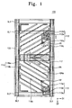
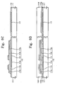
- FIG. 1 is a plan view showing a display panel according to an exemplary embodiment of the present invention.
- FIG. 2 is a cross-sectional view taken along lines I-I' and II-II' of FIG. 1 .
- the first, second, and third gate lines GL1, GL2, and GL3 extend in a first direction D1, and the first and second data lines DL1 and DL2 extend in a second direction D2, which is substantially perpendicular to the first direction D1.
- the second and third gate lines GL2 and GL3 and the first and second data lines DL1 and DL2 define the rectangular-shaped pixel area PA on the first base substrate 111.
- the first and second data lines DL1 and DL2 are arranged on a different layer than the first, second, and third gate lines GL1, GL2, and GL3, so that the first and second data lines DL1 and DL2 may be electrically insulated from the first, second, and third gate lines GL1, GL2, and GL3.
- the second black matrix 126a includes the same material as that of the first black matrix 122 (shown in FIG. 2 ) and is substantially simultaneously patterned together with the first black matrix 122 through one process.
- the dummy color filter 126b has the same color as that of one color filter of color filters adjacent to the green color filter G and is substantially simultaneously patterned together with the one color filter through one process.
- the dummy color filter 126b is a red (R) color filter R.
- a color filter substrate 120 includes a fourth protruding portion 128 arranged directly above the storage electrode 117, and the fourth protruding portion 128 includes a first dummy color filter 128a and a second dummy color filter 128b.
- a green color filter G is arranged on the color filter substrate 120 to cover the first dummy color filter 128a, and the second dummy color filter 128b is arranged on the green color filter G.
- a display panel 200 includes a first data line DL1, a second data line DL2, a first gate line GL1, a second gate line GL2, and a third gate line GL3.
- the first, second, and third gate lines GL1, GL2, and GL3 extend in a first direction D1
- the first and second data lines DL1 and DL2 extend in a second direction D2, which is substantially perpendicular to the first direction D1.
- a gate insulating layer 114 is formed on the first base substrate 111 to cover the first gate electrode 112a and the storage electrode 117.
- the gate insulating layer 114 may include an inorganic compound such as silicon nitride.
- An active layer 119a which includes an amorphous silicon layer, is coated on the gate insulating layer 114.
- An ohmic contact layer 119b which is doped with impurity ions, is coated on the active layer 119a.
- the gate insulating layer 114, the active layer 119a, and the ohmic contact layer 119b may be sequentially coated on an entire surface of the first base substrate 111 using a plasma chemical vapor deposition technique.
- a second photoresist pattern is formed.
- the data metal pattern and the pre-ohmic contact pattern are removed directly above the first gate metal 112a through an etching process using the second photoresist pattern as an etching mask.
- the first thin film transistor 112 is completed through the above-described processes. According to the above, the active pattern 112b, the ohmic contact pattern 112c, the first source electrode 112d, and the first drain electrode 112e are patterned using one mask, thereby simplifying the manufacturing process and reducing the manufacturing cost of a display panel.
- a first transparent insulating layer 119e and a second transparent insulating layer 119f are sequentially coated on the first thin film transistor 112 and the gate insulating layer 114.
- the second transparent insulating layer 119f includes a photosensitive acrylic resin so that the second transparent insulating layer 119f may be patterned through the photolithography process.
- the second transparent insulating layer 119f may have a negative type photoresist or a positive type photoresist.
- the second transparent insulating layer 119f including the positive type photoresist will be described as an example.
- a color filter layer 123 is formed over the second base substrate 121 to cover the first and second black matrices 122 and 125.
- the color filter layer 123 partially overlaps with the first black matrix 122 formed in a peripheral portion of the pixel area, but the color filter layer 123 covers an entire surface of the second black matrix 125 formed in the pixel area.
- the color filter layer 123 includes a red color filter, a green color filter, and a blue color filter.
- the red, green, and blue color filters may be sequentially formed through a patterning process or an inkjet printing method.
Landscapes
- Physics & Mathematics (AREA)
- Nonlinear Science (AREA)
- Mathematical Physics (AREA)
- Chemical & Material Sciences (AREA)
- Crystallography & Structural Chemistry (AREA)
- General Physics & Mathematics (AREA)
- Optics & Photonics (AREA)
- Engineering & Computer Science (AREA)
- Power Engineering (AREA)
- Microelectronics & Electronic Packaging (AREA)
- Liquid Crystal (AREA)
- Devices For Indicating Variable Information By Combining Individual Elements (AREA)
Description
- Field of the Invention
- The present invention relates to a display panel and a method of manufacturing the same. More particularly, the present invention relates to a display panel having a reduced manufacturing cost and a method of manufacturing the display panel.
- Discussion of the Background ,
- Generally, a liquid crystal display includes an array substrate, a color filter substrate facing the array substrate, and a liquid crystal layer interposed between the array substrate and the color filter substrate.
- The array substrate includes a plurality of pixels to display an image therethrough. Each pixel includes a gate line, a data line, a thin film transistor, a storage line, and a pixel electrode. The gate and data lines receive gate and data signals, respectively, and are coupled to gate and source electrodes of the thin film transistor, respectively. The pixel electrode is coupled to a drain electrode of the thin film transistor.
- The color filter substrate includes a color filter layer and a common electrode. The color filter layer includes red, green, and blue color filters. The common electrode is arranged on the color filter layer and faces the pixel electrode with the liquid crystal layer being interposed between the common electrode and the pixel electrode.
- The array substrate may be manufactured through a process using five masks or a process using four masks. In the five mask process, an active layer and an ohmic contact layer of the thin film transistor are patterned using a different mask from that used to pattern the transistor's source and drain electrodes. However, in the four mask process, the active layer, the ohmic contact layer, and the source and drain electrodes of the thin film transistor are sequentially patterned using only one mask. As a result, the four mask process is simpler than the five mask process.
- The array substrate completed through the process using four masks includes a storage capacitor that is defined by a storage electrode, a pixel electrode, and an insulating layer interposed between the storage electrode and the pixel electrode as the capacitor's dielectric. In order to increase the storage capacitor's capacitance, the insulating layer may be partially recessed toward the storage electrode. However, when the insulating layer is recessed, an amount of liquid crystal filled in the recessed portion of the insulating layer increases.
-
US-A-6 057 896 discloses a display panel as recited in the pre-characterising portion ofclaim 1.US 2002/003519 discloses a display panel wherein concave portions are arranged on a base substrate at an area corresponding to the storage electrode on an opposed array substrate to prevent unevenness of the cell gap. - The present invention provides a display panel having a uniform cell gap and a reduced manufacturing cost.
- The present invention also provides a method suitable for manufacturing the above display panel.
- Additional features of the invention will be set forth in the description which follows, and in part will be apparent from the description, or may be learned by practice of the invention.
- The present invention discloses a display panel as in
claim 1. - It is to be understood that both the foregoing general description and the following detailed description are exemplary and explanatory and are intended to provide further explanation of the invention as claimed.
- The accompanying drawings, which are included to provide a further understanding of the invention and are incorporated in and constitute a part of this specification, illustrate embodiments of the invention, and together with the description serve to explain the principles of the invention.
-
FIG. 1 is a plan view showing a display panel according to an exemplary embodiment of the present invention. -
FIG. 2 is a cross-sectional view taken along lines I-I' and II-II' ofFIG. 1 . -
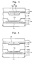
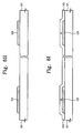
FIG. 3 is a cross-sectional view showing a storage electrode area of a display panel according to another exemplary embodiment of the present invention. -
FIG. 4 is a cross-sectional view showing a storage electrode area of a display panel according to another exemplary embodiment of the present invention. -
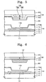
FIG. 5 is a cross-sectional view showing a storage electrode area of a display panel according to another exemplary embodiment of the present invention. -
FIG. 6 is a cross-sectional view showing a storage electrode area of a display panel according to another exemplary embodiment of the present invention. -
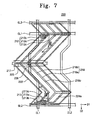
FIG. 7 is a plan view showing a display panel according to another exemplary embodiment of the present invention. -
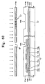
FIG. 8A, 8B ,8C, 8D ,8E ,8F, 8G ,8H, 8I, 8J, and 8K are cross-sectional views showing a process of manufacturing the display panel shown inFIG. 2 according to an exemplary embodiment of the present invention. - Exemplary embodiments of the invention are described more fully hereinafter with reference to the accompanying drawings, in which embodiments of the invention are shown. This invention may, however, be embodied in many different forms and should not be construed as limited to the embodiments set forth herein. Rather, these embodiments are provided so that this disclosure is thorough, and will fully convey the scope of the invention to those skilled in the art. In the drawings, the size and relative sizes of layers and regions may be exaggerated for clarity. Like reference numerals in the drawings denote like elements.
- It will be understood that when an element or layer is referred to as being "on", "connected to" or "coupled to" another element or layer, it can be directly on, connected or coupled to the other element or layer or intervening elements or layers may be present. In contrast, when an element is referred to as being "directly on", "directly connected to", or "directly coupled to" another element or layer, there are no intervening elements or layers present. As used herein, the term "and/or" includes any and all combinations of one or more of the listed items.
- It will be understood that, although the terms first, second, etc. may be used herein to describe various elements, components, regions, layers and/or sections, these elements, components, regions, layers and/or sections should not be limited by these terms. These terms are only used to distinguish one element, component, region, layer or section from another region, layer or section. Thus, a first element, component, region, layer or section discussed below could be termed a second element, component, region, layer or section without departing from the teachings of the present invention.
- The terminology used herein is for the purpose of describing particular embodiments only and is not intended to be limiting of the invention. As used herein, the singular forms, "a", "an" and "the" are intended to include the plural forms as well, unless the context clearly indicates otherwise. It will be further understood that the terms "includes" and/or "including", when used in this specification, specify the presence of stated features, integers, steps, operations, elements, and/or components, but do not preclude the presence or addition of one or more other features, integers, steps, operations, elements, components, and/or groups thereof.
- Unless otherwise defined, all terms (including technical and scientific terms) used herein have the same meaning as commonly understood by one of ordinary skill in the art to which this invention belongs. It will be further understood that terms, such as those defined in commonly used dictionaries, should be interpreted as having a meaning that is consistent with their meaning in the context of the relevant art and will not be interpreted in an idealized or overly formal sense unless expressly so defined herein.
-
FIG. 1 is a plan view showing a display panel according to an exemplary embodiment of the present invention.FIG. 2 is a cross-sectional view taken along lines I-I' and II-II' ofFIG. 1 . - Referring to
FIG. 1 andFIG. 2 , adisplay panel 100 includes anarray substrate 110, acolor filter substrate 120 facing thearray substrate 110, and aliquid crystal layer 300 interposed between thearray substrate 110 and thecolor filter substrate 120. - The
array substrate 110 includes afirst base substrate 111 and a plurality of pixels. A plurality of pixel areas is defined on thefirst base substrate 111 in a matrix configuration, and the pixels are arranged in the pixel areas, respectively. In the present exemplary embodiment, since the pixels have same structure and function, only one pixel among the pixels will be illustrated with reference toFIG. 1 andFIG. 2 , and detailed descriptions of the remaining pixels will be omitted. - A first data line DL1, a first gate line GL1, and a second gate line GL2 are arranged on the
first base substrate 111 and electrically coupled to the pixel. A third gate line GL3 and a second data line DL2 are further arranged on thefirst base substrate 111 and are electrically coupled to adjacent pixels. - The first, second, and third gate lines GL1, GL2, and GL3 extend in a first direction D1, and the first and second data lines DL1 and DL2 extend in a second direction D2, which is substantially perpendicular to the first direction D1. The second and third gate lines GL2 and GL3 and the first and second data lines DL1 and DL2 define the rectangular-shaped pixel area PA on the
first base substrate 111. The first and second data lines DL1 and DL2 are arranged on a different layer than the first, second, and third gate lines GL1, GL2, and GL3, so that the first and second data lines DL1 and DL2 may be electrically insulated from the first, second, and third gate lines GL1, GL2, and GL3. - The pixel arranged in the pixel area PA includes a first
thin film transistor 112, a second thin film transistor 113, agate insulating layer 114, apassivation layer 115, an organic insulatinglayer 116, astorage electrode 117, and apixel electrode 118. - The first
thin film transistor 112 includes afirst gate electrode 112a, a firstactive pattern 112b, a firstohmic contact pattern 112c, afirst source electrode 112d, and afirst drain electrode 112e. - The
first gate electrode 112a branches from the first gate line GL1 and is arranged on thefirst base substrate 111. Thefirst gate electrode 112a is covered by thegate insulating layer 114. The firstactive pattern 112b and the firstohmic contact pattern 112c are sequentially formed on thegate insulating layer 114. The firstohmic contact pattern 112c is partially removed above thefirst gate electrode 112a. Thefirst source electrode 112d and thefirst drain electrode 112e are formed on theohmic contact pattern 112c and spaced apart from each other in the area where the firstohmic contact pattern 112c is partially removed. - The second thin film transistor 113 includes a
second gate electrode 113a, a second active pattern (not shown), a second ohmic contact pattern (not shown), a second source electrode 113d, and asecond drain electrode 113e. -
FIG. 2 shows a cross-sectional view of the firstthin film transistor 112. The second thin film transistor 113 has the same cross-sectional structure as the firstthin film transistor 112. - The
second gate electrode 113a of the second thin film transistor 113 branches from the second gate line GL2 and is arranged on thefirst base substrate 111. Thesecond gate electrode 113a is covered by thegate insulating layer 114. The second active pattern and the second ohmic contact pattern are sequentially formed on thegate insulating layer 114, and the second ohmic contact pattern is partially removed above thesecond gate electrode 113a. The second source electrode 113d and thesecond drain electrode 113e are formed on the second ohmic contact pattern and spaced apart from each other in the area where the second ohmic contact pattern is partially removed. - The
storage electrode 117 includes the same material as the first andsecond gate electrodes storage electrode 117 has a rectangular shape and extends in thefirst direction D 1. Thestorage electrode 117 is covered by thegate insulating layer 114, which is arranged over the pixel area PA. - The
passivation layer 115 covers thegate insulating layer 114 and the first and secondthin film transistors 112 and 113. The organic insulatinglayer 116 is arranged on thepassivation layer 115. Thepassivation layer 115 and the organic insulatinglayer 116 include first and second contact holes H1 and H2 exposing the first andsecond drain electrodes layer 116 is recessed directly above thestorage electrode 117 in a predetermined depth. Thus, the organic insulatinglayer 116 includes aconcave portion 116c that is defined directly above thestorage electrode 117. - The
pixel electrode 118 is arranged on the organic insulatinglayer 116. Thepixel electrode 118 has a symmetrical shape in plan view with respect to thestorage electrode 117, which is positioned at a central portion of the pixel area PA. - The
pixel electrode 118 and thestorage electrode 117 define a storage capacitor Cst together with the organic insulatinglayer 116, thepassivation layer 115, and thegate insulating layer 114, which serve as the capacitor's dielectric substance. The organic insulatinglayer 116 may be completely or partially removed directly above thestorage electrode 117. Therefore, a capacitance of the storage capacitor Cst may increase in proportion to the reduced thickness of the organic insulatinglayer 116. - The
pixel electrode 118 includes a firstsub pixel electrode 118a to receive a first pixel voltage and a secondsub pixel electrode 118b to receive a second pixel voltage, which is smaller than the first pixel voltage. The first and secondsub pixel electrodes - The first
sub pixel electrode 118a is electrically coupled to thefirst drain electrode 112e through the first contact hole H1, and the secondsub pixel electrode 118b is electrically coupled to thesecond drain electrode 113e through the second contact hole H2. When the firstthin film transistor 112 turns on in response to a first gate signal applied through the first gate line GL1, the first pixel voltage is supplied to the firstsub pixel electrode 118a via the firstthin film transistor 112 and the firstdata line DL 1. Then, when the second thin film transistor 113 turns on in response to a second gate signal applied through the second gate line GL2, the second pixel voltage is supplied to the secondsub pixel electrode 118b via the second thin film transistor 113 and the first data line DL1. - As the first and second
sub pixel electrodes sub pixel electrodes sub pixel electrodes display panel 100 through a mutual compensation between light characteristics. - As
FIG. 1 shows, the firstsub pixel electrode 118a may have a V-shape rotated in a clockwise direction and is partially overlapped with thestorage electrode 117. The firstsub pixel electrode 118a is symmetrically positioned relative to thestorage electrode 117. The secondsub pixel electrode 118b is arranged in the remaining pixel area PA. - The first and second
sub pixel electrodes first opening patterns 118c. Thefirst opening patterns 118c are formed through the secondsub pixel electrode 118b and spaced apart from each other by a predetermined distance. Thefirst opening patterns 118c divide the pixel area PA into a plurality of domains. - The
color filter substrate 120 facing thearray substrate 110 includes asecond base substrate 121, a firstblack matrix 122, acolor filter layer 123, acommon electrode 124, a first protrudingportion 125, and acolumn spacer 135. - The first
black matrix 122 includes a light blocking material and is arranged on thesecond base substrate 121. AsFIG. 1 shows, the firstblack matrix 122 is arranged directly above the first and seconddata lines DL 1 and DL2 and the first and secondthin film transistors 112 and 113. The firstblack matrix 122 prevents light from leaking through an area that is adjacent to the pixel area PA. - The
color filter layer 123 includes red, green, and blue color filters, and the red, green, and blue color filters are arranged in areas corresponding to the pixel areas PA of thearray substrate 110, respectively.FIG. 2 shows the green color filter G corresponding to one pixel area PA of the pixel areas PA. - The
common electrode 124 is arranged on thecolor filter layer 123 with a uniform thickness. Pluralsecond opening patterns 124a are formed through thecommon electrode 124 and spaced apart from each other by a predetermined distance. Eachfirst opening pattern 118c in thepixel electrode 118 is disposed between two adjacentsecond opening patterns 124a. The first andsecond opening patterns - The
liquid crystal layer 300 is interposed between thearray substrate 110 and thecolor filter substrate 120, and liquid crystal molecules of theliquid crystal layer 300 provided in different domains align in different directions from each other. Thus, a viewing angle of thedisplay panel 100 may be improved. - The
column spacer 135 is arranged on thecommon electrode 124 and interposed between thearray substrate 110 andcolor filter substrate 120 to maintain a gap between thearray substrate 110 and thecolor filter substrate 120. Thus, liquid crystals may be injected into the space defined between thearray substrate 110 and thecolor filter substrate 120. - Although an image is not displayed on area where the
storage electrode 117 is arranged because thestorage electrode 117 blocks light, the liquid crystals are also injected in that area. The first protrudingportion 125 is arranged on thesecond base substrate 121 to protrude toward thearray substrate 110 to prevent excess liquid crystals from accumulating at theconcave portion 116c. - In the present exemplary embodiment, the first protruding
portion 125 includes a second black matrix, which is made of the same material as that of the firstblack matrix 122 and is substantially simultaneously patterned with the firstblack matrix 122 through the same process. As noted above, since thestorage electrode 117 does not transmit light, an opening ratio of thedisplay panel 100 does not decrease when the first protrudingportion 125 is formed as the second black matrix directly above thestorage electrode 117. - The height of the first protruding
portion 125 is equal to or less than the depth of theconcave portion 116c. The width of the first protrudingportion 125 is equal to or less than the width of thestorage electrode 117. In the present exemplary embodiment, the height of the first protrudingportion 125 is substantially the same as the thickness of the firstblack matrix 122. - As the first protruding
portion 125 is arranged at an area of thecolor filter substrate 120 corresponding to thestorage electrode 117, a thickness of theliquid crystal layer 300 may be reduced in proportion to the height of the first protrudingportion 125 at theconcave portion 116c. Thus, the amount of the liquid crystals at theconcave portion 116c may be decreased, thereby reducing a total amount of the liquid crystal. - The first protruding
portion 125 uniformly maintains a cell-gap (i.e., a distance between thearray substrate 110 and the color filter substrate 120) of thedisplay panel 100. As the height of the first protrudingportion 125 is controlled in proportion to the depth of theconcave portion 116c, the cell-gap of thedisplay panel 100 may be uniformly maintained, thereby improving the display quality of thedisplay panel 100. -
FIG. 3 is a cross-sectional view showing a storage electrode area of a display panel according to another exemplary embodiment of the present invention. InFIG. 3 , the same reference numerals denote the same elements inFIG. 2 , and thus detailed descriptions of the same elements will be omitted. - Referring to
FIG. 3 , a second protrudingportion 126 arranged on thecolor filter substrate 120 at an area corresponding to thestorage electrode 117 includes a secondblack matrix 126a and adummy color filter 126b. A green color filter G is arranged on thecolor filter substrate 120 to cover the second protrudingportion 126. - The second
black matrix 126a includes the same material as that of the first black matrix 122 (shown inFIG. 2 ) and is substantially simultaneously patterned together with the firstblack matrix 122 through one process. Thedummy color filter 126b has the same color as that of one color filter of color filters adjacent to the green color filter G and is substantially simultaneously patterned together with the one color filter through one process. In the present exemplary embodiment, thedummy color filter 126b is a red (R) color filter R. - When the second protruding
portion 126 includes thedummy color filter 126b, the height of the second protrudingportion 126 exceeds that of the first protrudingportion 125 shown inFIG. 2 . Therefore, the thickness of theliquid crystal layer 300 may be further reduced at theconcave portion 116c, thereby reducing a total amount of the liquid crystal injected into thedisplay panel 100. -
FIG. 4 is a cross-sectional view showing a storage electrode area of a display panel according to another exemplary embodiment of the present invention.FIG. 5 is a cross-sectional view showing a storage electrode area of a display panel according to another exemplary embodiment of the present invention. InFIG. 4 andFIG. 5 , the same reference numerals denote the same elements as inFIG. 2 , and detailed descriptions of the same elements will be omitted. - Referring to
FIG. 4 , acolor filter substrate 120 includes a third protrudingportion 127 arranged at an area corresponding to aconcave portion 116c of an organic insulatinglayer 116, and the third protrudingportion 127 serves as a first dummy color filter. A green color filter G is arranged on thecolor filter substrate 120 to cover the third protrudingportion 127. - The first dummy color filter has the same color as that of one color filter of color filters adjacent to the green color filter G and is substantially simultaneously patterned together with the one color filter through one process. In the present exemplary embodiment, the first
dummy color filter 127 is a red color filter R. - Referring to
FIG. 5 , acolor filter substrate 120 includes a fourth protrudingportion 128 arranged directly above thestorage electrode 117, and the fourth protrudingportion 128 includes a firstdummy color filter 128a and a seconddummy color filter 128b. A green color filter G is arranged on thecolor filter substrate 120 to cover the firstdummy color filter 128a, and the seconddummy color filter 128b is arranged on the green color filter G. - The first
dummy color filter 128a has the same color as that of one selected color filter of color filters adjacent to the green color filter G, and the seconddummy color filter 128b has the same color as that of the remaining color filter adjacent to the green color filter G. The first and seconddummy color filters dummy color filter 128a is a red color filter R, and the seconddummy color filter 128b is a blue color filter B. - As shown in
FIG. 4 andFIG. 5 , a thickness of theliquid crystal layer 300 corresponding to theconcave portion 116c of the organic insulatinglayer 116 may be reduced by the third and fourth protrudingportions concave portion 116c may be reduced. -
FIG. 6 is a cross-sectional view showing a storage electrode area of a display panel according to another exemplary embodiment of the present invention. InFIG. 6 , the same reference numerals denote the same elements as inFIG. 2 , and thus detailed descriptions of the same elements will be omitted. - Referring to
FIG. 6 , acolor filter substrate 120 includes a fifth protrudingportion 137 arranged thereon at an area corresponding to thestorage electrode 117, and the fifth protrudingportion 137 serves as a dummy column spacer. Thedummy column spacer 137 includes the same material as that of thecolumn spacer 135 shown inFIG. 2 and is substantially simultaneously patterned with thecolumn spacer 135 through one manufacturing process. - The height of the
dummy column spacer 137 may be less than that of thecolumn spacer 135. Thedummy column spacer 137 may be patterned using a silt mask when forming thecolumn spacer 135, so that thedummy column spacer 137 is lower than thecolumn spacer 135. In the present exemplary embodiment, the height of thedummy column spacer 137 may be equal to or less than a depth of aconcave portion 116c of the organic insulatinglayer 116. - As the
dummy column spacer 137 is arranged on thecolor filter substrate 120, a thickness of theliquid crystal layer 300 may be reduced at theconcave portion 116c. As a result, an amount of liquid crystal in theconcave portion 116c may be decreased. -
FIG. 7 is a plan view showing a display panel according to another exemplary embodiment of the present invention. - Referring to
FIG. 7 , adisplay panel 200 includes a first data line DL1, a second data line DL2, a first gate line GL1, a second gate line GL2, and a third gate line GL3. The first, second, and third gate lines GL1, GL2, and GL3 extend in a first direction D1, and the first and second data lines DL1 and DL2 extend in a second direction D2, which is substantially perpendicular to the first direction D1. - The
display panel 200 further includes a firstthin film transistor 212, a second thin film transistor 213, astorage electrode 217, and apixel electrode 218. The firstthin film transistor 212 is electrically coupled to the first gate line GL1 and the first data line DL1, and the second thin film transistor 213 is electrically coupled to the second gate line GL2 and the first data line DL1. - The
pixel electrode 218 is arranged between the second gate line GL2 and the third gate line GL3, and thestorage electrode 217 extends in the first direction D1 between the first gate line GL1 and the third gate line GL3 at a central portion of the pixel. Thepixel electrode 218 has a zigzag shape and is symmetrically arranged with respect to thestorage electrode 217. - The
pixel electrode 218 includes a firstsub pixel electrode 218a and a secondsub pixel electrode 218b. The firstsub pixel electrode 218a has a V-shape rotated in a clockwise direction and is symmetrically arranged with respect to thestorage electrode 217. The secondsub pixel electrode 218b is arranged in the remaining area of the pixel. The firstsub pixel electrode 218a is electrically coupled to the firstthin film transistor 212, and the secondsub pixel electrode 218b is electrically coupled to the second thin film transistor 213. Also, the first and secondsub pixel electrodes - A
first opening pattern 218c is formed between the first and secondsub pixel electrodes sub pixel electrodes pixel electrode 218 in a predetermined area. As a result, the first data line DL1 partially overlaps with thefirst opening pattern 218c in the pixel area. - The
display panel 200 includes a firstblack matrix 222 that is arranged in a peripheral portion adjacent to the pixel area to prevent light from leaking through the peripheral portion. Thedisplay panel 200 also includes a thirdblack matrix 229 and a fourthblack matrix 225. The thirdblack matrix 229 is positioned in an area where the first data line DL1 and thefirst opening pattern 218c overlap with each other. The fourthblack matrix 225 extends substantially parallel to thestorage electrode 217 in the first direction D1. The thirdblack matrix 229 prevents light from leaking through the area where the firstdata line DL 1 and thefirst opening pattern 218c overlap with each other. The fourthblack matrix 225 branches from the thirdblack matrix 229 and is arranged directly above thestorage electrode 217. - As described in with reference to
FIG. 1 andFIG. 2 , an organic insulating layer is recessed in a predetermined depth directly abovestorage electrode 217 to increase a capacitance of a storage capacitor. The fourthblack matrix 225 protrudes toward thestorage electrode 217 directly above theconcaved portion 116c of the organic insulatinglayer 116. The fourthblack matrix 225 may prevent an excessive amount of liquid crystals from accumulating at theconcaved portion 116c, so that the total amount of the liquid crystals injected into thedisplay panel 200 may be reduced. - As an example of the present embodiment, the width of the fourth
black matrix 225 is equal to or less than that of thestorage electrode 217. Also, the fourthblack matrix 225 and the firstblack matrix 222 may have the same thickness. Therefore, the fourthblack matrix 225 may reduce the amount of liquid crystals needed for the liquid crystal layer without decreasing an opening ratio of thedisplay panel 200. -
FIG. 7 shows the fourthblack matrix 225 arranged directly above thestorage electrode 217 in the case of a zigzag-shapedpixel electrode 218. However, thedisplay panel 200 may have various protruding portions having different structures as shown inFIG. 3, FIG. 4 ,FIG. 5, and FIG. 6 arranged in the area corresponding to thestorage electrode 217. -
FIG. 8A, 8B ,8C, 8D ,8E ,8F, 8G ,8H, 8I ,8J, and 8K are cross-sectional views showing a method of manufacturing the display panel shown inFIG. 2 . As the firstthin film transistor 112 and the second thin film transistor 113 may be manufactured through the same process, the manufacturing processes for the firstthin film transistor 112 will be described with reference toFIGS. 8A to 8K , and the manufacturing processes for the second thin film transistor 113 will be omitted. - Referring to
FIG. 8A , afirst gate electrode 112a and astorage electrode 117 may be formed on afirst base substrate 111 by coating a gate metal layer over thefirst base substrate 111 and patterning the gate metal layer using a first mask (not shown). The gate metal layer may include a metallic material such as copper (Cu), aluminum (Al), silver (Ag), chromium (Cr), or a metal alloy. The gate metal layer may be etched through a wet etching process using etchant. - Referring to
FIG. 8B , agate insulating layer 114 is formed on thefirst base substrate 111 to cover thefirst gate electrode 112a and thestorage electrode 117. Thegate insulating layer 114 may include an inorganic compound such as silicon nitride. Anactive layer 119a, which includes an amorphous silicon layer, is coated on thegate insulating layer 114. Anohmic contact layer 119b, which is doped with impurity ions, is coated on theactive layer 119a. Thegate insulating layer 114, theactive layer 119a, and theohmic contact layer 119b may be sequentially coated on an entire surface of thefirst base substrate 111 using a plasma chemical vapor deposition technique. - A
data metal layer 119c is coated on theohmic contact layer 119b. Thedata metal layer 119c, theohmic contact layer 119b, and theactive layer 119a are patterned through a photolithography process. Although not shown in figures, a first photoresist pattern is formed on thedata metal layer 119c. In order to form the first photoresist pattern, a photoresist layer is coated on thedata metal layer 119c and exposed to light using a second mask (not shown) before developing the exposed photoresist layer. - The first photoresist pattern has different thicknesses in accordance with positions thereof. The first photoresist pattern is relatively thinner in an area corresponding to the
first gate electrode 112a. The second mask may be a slit mask or a halftone mask. - Then, the
data metal layer 119c, theohmic contact layer 119b, and theactive layer 119a are sequentially etched through an etching process using the first photoresist pattern as an etching mask. A data metal pattern, a pre-ohmic contact pattern, and an active pattern are formed through the etching process. Here, the data metal pattern, the pre-ohmic contact pattern, and the active pattern have the same structure. - When the first photoresist pattern is uniformly removed, a second photoresist pattern is formed. The data metal pattern and the pre-ohmic contact pattern are removed directly above the
first gate metal 112a through an etching process using the second photoresist pattern as an etching mask. - Referring to
FIG. 8C , afirst source electrode 112d, afirst drain electrode 112e, and anohmic contact pattern 112c are formed above thefirst gate electrode 112a through the etching process. Theohmic contact pattern 112c is divided into two portions that are coupled to thefirst source electrode 112d and thefirst drain electrode 112e, respectively. Theactive pattern 112b is formed under theohmic contact pattern 112c. - The first
thin film transistor 112 is completed through the above-described processes. According to the above, theactive pattern 112b, theohmic contact pattern 112c, thefirst source electrode 112d, and thefirst drain electrode 112e are patterned using one mask, thereby simplifying the manufacturing process and reducing the manufacturing cost of a display panel. - Referring to
FIG. 8D , a first transparent insulatinglayer 119e and a second transparent insulatinglayer 119f are sequentially coated on the firstthin film transistor 112 and thegate insulating layer 114. The second transparent insulatinglayer 119f includes a photosensitive acrylic resin so that the second transparent insulatinglayer 119f may be patterned through the photolithography process. The second transparent insulatinglayer 119f may have a negative type photoresist or a positive type photoresist. In the present exemplary embodiment, the second transparent insulatinglayer 119f including the positive type photoresist will be described as an example. - Referring to
FIG. 8E , the second transparent insulatinglayer 119f is exposed using athird mask 119d. Thethird mask 119d includes a transmissive portion OP1, a slit transmissive portion SL1, and a light blocking portion. Thethird mask 119d may include a slit mask. - The second transparent insulating
layer 119f is completely removed from an area corresponding to the transmissive portion OP1 and partially removed from an area corresponding to the slit transmissive portion SL1, thereby forming an organicinsulating pattern 119g that has afirst opening portion 116a corresponding to the transmissive portion OP1 and afirst groove 116b corresponding to the slit transmissive portion SL1. Thefirst groove 116b is formed directly above thestorage electrode 117. - Then, the first transparent insulating
layer 119e is etched using the organic insulatingpattern 119g as an etching mask. - Referring to
FIG. 8F , the first transparent insulatinglayer 119e is removed in an area corresponding to thefirst opening portion 116a through the etching process, thereby forming apassivation layer 115 having a first contact hole H1. Thefirst drain electrode 112e of the firstthin film transistor 112 is exposed through the first contact hole H1. - Also, the organic insulating
pattern 119g is uniformly removed in a predetermined thickness, thereby forming an organic insulatinglayer 116. The organicinsulating pattern 119g may be completely or partially removed at a position corresponding to thefirst groove 116b. As shown inFIG. 8F , the organic insulatinglayer 116 is partially removed at the position, so that the organic insulatinglayer 116 has aconcave portion 116c concaved toward thestorage electrode 117. - Referring to
FIG. 8G , a transparent conductive layer (not shown) is formed on the organic insulatinglayer 116 and patterned by an etching process using a fourth mask (not shown), thereby forming a firstsub pixel electrode 118a and a secondsub pixel electrode 118b on the organic insulatinglayer 116. The first and secondsub pixel electrodes first opening pattern 118c. - The first
sub pixel electrode 118a is electrically coupled to thefirst drain electrode 112e of the firstthin film transistor 112 via the first contact hole H1. Also, the firstsub pixel electrode 118a faces thestorage electrode 117. The organic insulatinglayer 116, thepassivation layer 115, and thegate insulating layer 114 are interposed between the firstsub pixel electrode 118a and thestorage electrode 117 and serve as a dielectric substance of the storage capacitor. - The array substrate 110 (shown in
FIG. 2 ) is completed through the above-described processes, and the color filter substrate 120 (shown inFIG. 2 ) is manufactured through the below processes. - Referring to
FIG. 8H , a firstblack matrix 122 and a secondblack matrix 125 are formed on asecond base substrate 121 by forming and patterning a light blocking layer (not shown) that includes chromium (Cr) or organic material . The firstblack matrix 122 is formed in an area corresponding to the firstthin film transistor 112 and the first data line DL1, and the secondblack matrix 125 is formed in an area corresponding to thestorage electrode 117. - Referring to
FIG. 8I , acolor filter layer 123 is formed over thesecond base substrate 121 to cover the first and secondblack matrices color filter layer 123 partially overlaps with the firstblack matrix 122 formed in a peripheral portion of the pixel area, but thecolor filter layer 123 covers an entire surface of the secondblack matrix 125 formed in the pixel area. Thecolor filter layer 123 includes a red color filter, a green color filter, and a blue color filter. The red, green, and blue color filters may be sequentially formed through a patterning process or an inkjet printing method. - Referring to
FIG. 8J , a transparent conductive layer (not shown) is formed on thecolor filter layer 123 and patterned, thereby forming acommon electrode 124 on thecolor filter layer 123. Asecond opening pattern 124a is formed through thecommon electrode 124 through the above-described patterning process. - Referring to
FIG. 8K , an insulating layer (not shown) that has the same thickness as a predetermined cell-gap is deposited on thecommon electrode 124. The insulating layer is patterned to form acolumn spacer 135 on thecommon electrode 124. AsFIG. 8K shows, thecolumn spacer 135 is formed above the firstblack matrix 122. Therefore, thecolumn spacer 135 may maintain the cell-gap of the display panel 100 (shown inFIG. 1 ) without reducing an opening ratio of thedisplay panel 100. - The
color filter substrate 120 completed through the above-described processes is combined with thearray substrate 110. The liquid crystals may be dropped on thecolor filter substrate 120 before thecolor filter substrate 120 and thearray substrate 110 are assembled with each other. Thus, the amount of the liquid crystals at theconcave portion 116c may be reduced due to the secondblack matrix 125, thereby reducing the total amount of the liquid crystals dropped on thecolor filter substrate 120. - As another example of the present embodiment, the liquid crystals may be injected between the
array substrate 110 and thecolor filter substrate 120 after assembling thearray substrate 110 with thecolor filter substrate 120. The secondblack matrix 125 reduces a distance between thearray substrate 110 and thecolor filter substrate 120, so that an amount of the liquid crystals may be reduced at theconcave portion 116c. - As described above, the organic insulating layer formed on the array substrate has the concave portion directly above the storage electrode, and the protruding portion formed on the color filter substrate protrudes toward the concave portion.
- Thus, the amount of the liquid crystals at the concave portion may be reduced, so that the total amount of liquid crystal needed for the display panel may be also reduced. Further, the display panel may have a uniform cell-gap due to the protruding portion formed corresponding to the concave portion.
- It will be apparent to those skilled in the art that various modifications and variation can be made in the present invention without departing from the scope of the invention. Thus, it is intended that the present invention cover the modifications and variations of this invention provided they come within the scope of the appended claims.
Claims (23)
- A display panel (100), comprising:an array substrate (110) comprising:a first base substrate (111) comprising a plurality of pixel areas (PA);a gate electrode (112a,113a) and a storage electrode (117) arranged in each pixel area of the first base substrate (111);a gate insulating layer (114) arranged on the first base substrate (111) to cover the gate electrode (112a,113a) and the storage electrode (117), an insulating layer (116) comprising a concave portion (116a) formed at a position corresponding to the storage electrode (117); anda pixel electrode (118) arranged on the gate insulating layer (114) and facing the storage electrode (117);an opposite substrate comprising:a second base substrate (121) facing the first base substrate (111); anda liquid crystal layer (300) interposed between the array substrate (110) and the opposite substrate (120), characterised in that a protruding portion (125;126; 127;128;137) is arranged on the second base substrate (121) at an area corresponding to the storage electrode (117) and protrudes toward the first base substrate (111) so as to maintain a substantially uniform cell gap.
- The display panel (100) of claim 1, wherein the opposite substrate (120) further comprises a first black matrix (122) arranged on the second base substrate (121) at a position corresponding to a peripheral area adjacent to the pixel areas (PA).
- The display panel (100) of claim 2, wherein the protruding portion (125; 126) comprises a second black matrix (125; 126a), the second black matrix (125; 126a) comprising the same material as that of the first black matrix (122).
- The display panel (100) of claim 3, wherein the opposite substrate (120) further comprises a color filter layer (123) comprising color filters (R; G; B) corresponding to the pixel areas (PA), respectively, and the color filters (R; G; B) cover the second black matrix (125; 126a).
- The display panel (100) of claim 4, wherein the protruding portion (126) further comprises a dummy color filter (126b) arranged between the second black matrix (126a) and one color filter (R) among the color filters arranged above the second black matrix (126a), the dummy color filter (126b) having the same color as that of at least one color filter of the color filters that are adjacent to the one color filter (R).
- The display panel (100) of claim 5, wherein the opposite substrate (120) further comprises a common electrode (124) arranged on the color filter laver (123).
- The display panel (100) of claim 1, wherein the opposite substrate (120) further comprises a color filter layer (123) comprising color filters (R; G; B) corresponding to the pixel areas (PA), respectively.
- The display panel (100) of claim 7, wherein the protruding portion (128) comprises a first dummy color filter (128a) arranged between a corresponding color filter (G) among the color filters and the second base substrate (121), and the first dummy color filter (128a) has the same color as that of one of the color filters (R; B) that are adjacent to the corresponding color filter (G).
- The display panel (100) of claim 8, wherein the protruding portion (128) further comprises a second dummy color filter (128b) arranged on the corresponding color filter (G), the second dummy color filter (128b) having the same color as that of one color filter of the adjacent color filters (R; B) and different from that of the first dummy color filter (128a).
- The display panel of claim 8, wherein the opposite substrate (120) further comprises a common electrode (124) arranged on the color filter laver (123).
- The display panel (100) of claim 7, wherein the opposite substrate (120) further comprises:a common electrode (124) arranged on the color filter layer (123); anda column spacer (135) arranged on the common electrode (124) to maintain a gap between the array substrate (110) and the opposite substrate (120), andthe protruding portion (137) comprises a dummy column spacer (137) arranged on the common electrode (124) at a position corresponding to the storage electrode (117).
- The display panel (100) of claim 11, wherein the dummy column spacer (137) the same material as that of the column spacer (135), and a height of the dummy column spacer (137) is less than that of the column spacer (135).
- The display panel (100) of claim 1, wherein a height of the protruding portion (125; 126; 127; 128; 137) is equal to or less than a depth of the concave portion of the insulating layer.
- The display panel (100) of claim 1, wherein the insulating layer comprises:a gate insulating layer (114) covering the storage electrode (117);a passivation layer (115) arranged on the gate insulating layer (114); andan organic insulating layer (116) arranged on the passivation layer (115), the organic insulating layer (116) comprising the concave portion (116).
- The display panel (100) of claim 1, wherein the pixel electrode (118) comprises:a first sub pixel electrode (118a) to receive a first pixel voltage; anda second sub pixel electrode (118b) to receive a second pixel voltage, the second pixel voltage being smaller than the first pixel voltage.
- The display panel (100) of claim 15, wherein the pixel electrode (118) comprises a plurality of first openings (118c) formed therethrough to electrically separate the first sub pixel electrode (118a) and the second sub pixel electrode (118b) from each other and to divide each pixel area into a plurality of domains.
- The display panel (100) of claim 16, wherein the opposite substrate (120) further comprises a common electrode (124) facing the pixel electrode (118), the common electrode (124) comprising a plurality of second openings (124a) formed therethrough, the second openings (124a) being arranged in different positions from those of the first openings (118c) to divide the domains.
- The display panel (100) of claim 15, wherein the array substrate (110) further comprises:a first gate line (GL1):a second gate line (GL2) spaced apart from the first gate line (GL1);a data line (DL1; DL2) crossing with and electrically insulated from the first gate line (GL1) and the second gate line (GL2);a first thin film transistor (112) electrically coupled to the first gate line (GL1) and the data line (DL1; DL2) to output the first pixel voltage; anda second thin film transistor (113) electrically coupled to the second gate line (GL2) and the data line (DL1; DL2) to output the second pixel voltage.
- The display panel (100) of claim 18, wherein the first sub pixel electrode (118a) is electrically coupled to an output electrode of the first thin film transistor (112) to receive the first pixel voltage, and the second sub pixel electrode (118b) is electrically coupled to an output electrode of the second thin film transistor (113) to receive the second pixel voltage.
- A method of manufacturing a display panel (100), comprising:forming a gate electrode (112a; 113a) and a storage electrode (117) in a pixel area (PA) of a first base substrate (111):forming a gate insulating layer (114) on the first base substrate (111) to cover the gate electrode (112a; 113a) and the storage electrode (117);forming an active pattern (112b), an ohmic contact pattern (112c), a source electrode (112d; 113d), and a drain electrode (112e; 113e) on the gate insulating layer (114), the source electrode (112d; 113d) and the drain electrode (112e; 113e) having the same shape as that of the ohmic contact pattern (112c);forming an insulating layer (116) to cover the source electrode (112d; 113d) and the drain electrode (112e; 113e) and comprising a concave portion (116c) formed at a position corresponding to the storage electrode (117);forming a pixel electrode (118) on the insulating layer;forming a protruding portion (125; 126; 127; 128; 137) on a second base substrate (121);coupling the first base substrate (111) and the second base substrates (121) to each other such that the second base substrate (121) faces the first base substrate (111) with the protruding portion (125; 128; 127; 128; 137) protruding toward the storage electrode (117) so as to maintain a substantially uniform call gap; andinterposing a liquid crystal layer (300) between the first base substrate (111) and the second base substrate (121).
- The method of claim 20, wherein forming the protruding portion (125; 126; 127; 128; 137) comprises;coating a light blocking layer on the second base substrate (121); andpatterning the light blocking layer to form a first black matrix (122) In an area corresponding to a peripheral area of the pixel area (PA) and a second black matrix (125; 126a) in an area corresponding to the storage electrode (117).
- The method of claim 21, further comprising forming a first color filter (G) among color filters (R; G; B) having different colors from each other on the second base substrate (121), and wherein forming the protruding portion (126; 128) further comprises forming a second color filter (R) among the color filters on the first color filter, the second color filter (R) having a different color from that of the first color filter (G) and being formed at a position corresponding to the storage electrode (117).
- The method of claim 22, further comprising forming a common electrode (124) on the color filter and the protruding portion (125; 126; 127; 128; 137).
Applications Claiming Priority (1)
| Application Number | Priority Date | Filing Date | Title |
|---|---|---|---|
| KR1020060099408A KR101299646B1 (en) | 2006-10-12 | 2006-10-12 | Display panel and method of manufacturing the same |
Publications (2)
| Publication Number | Publication Date |
|---|---|
| EP1912095A1 EP1912095A1 (en) | 2008-04-16 |
| EP1912095B1 true EP1912095B1 (en) | 2010-05-19 |
Family
ID=38814638
Family Applications (1)
| Application Number | Title | Priority Date | Filing Date |
|---|---|---|---|
| EP07019888A Active EP1912095B1 (en) | 2006-10-12 | 2007-10-11 | Display panel manufacture |
Country Status (6)
| Country | Link |
|---|---|
| US (1) | US7742116B2 (en) |
| EP (1) | EP1912095B1 (en) |
| JP (1) | JP5415687B2 (en) |
| KR (1) | KR101299646B1 (en) |
| CN (1) | CN101201521B (en) |
| DE (1) | DE602007006605D1 (en) |
Families Citing this family (20)
| Publication number | Priority date | Publication date | Assignee | Title |
|---|---|---|---|---|
| KR20070075808A (en) * | 2006-01-16 | 2007-07-24 | 삼성전자주식회사 | Method for manufacturing display substrate and display substrate manufactured by the same |
| TW200924107A (en) * | 2007-10-02 | 2009-06-01 | Polymer Vision Ltd | An electronic circuit element with profiled photopatternable dielectric layer |
| RU2478225C2 (en) * | 2008-08-27 | 2013-03-27 | Шарп Кабусики Кайся | Active matrix substrate, liquid crystal panel, liquid crystal display unit, liquid crystal display device, television receiver and method of manufacturing active matrix substrate |
| CN102132202A (en) * | 2008-08-27 | 2011-07-20 | 夏普株式会社 | Active matrix substrate, liquid crystal panel, liquid crystal display device, liquid crystal display unit and television receiver |
| KR101247936B1 (en) * | 2008-08-27 | 2013-03-26 | 샤프 가부시키가이샤 | Active matrix substrate, liquid crystal panel, liquid crystal display unit, liquid crystal display device, television receiver, and active matrix substrate manufacturing method |
| CN101728398A (en) * | 2008-10-28 | 2010-06-09 | 奇美电子股份有限公司 | Thin film transistor substrate, display panel, display device and manufacturing method thereof |
| TWI400524B (en) * | 2008-12-02 | 2013-07-01 | Chunghwa Picture Tubes Ltd | Liquid crystal display process panel and method for forming alignment film |
| US8547513B2 (en) * | 2010-08-10 | 2013-10-01 | Lg Display Co., Ltd. | Liquid crystal display device and method of manufacturing the same |
| KR101778009B1 (en) * | 2010-08-19 | 2017-09-27 | 삼성디스플레이 주식회사 | Display panel and fabricating method thereof |
| CN102566157B (en) * | 2010-12-16 | 2014-10-08 | 京东方科技集团股份有限公司 | Array substrate and liquid crystal display |
| KR101859483B1 (en) * | 2012-03-06 | 2018-06-27 | 엘지디스플레이 주식회사 | Stereoscopic display device and method for manufacturing the same |
| KR101425611B1 (en) * | 2012-07-04 | 2014-07-31 | 엘지디스플레이 주식회사 | A Patterned Retarder Type Stereoscopic Image Display Device and Method for Manufacturing The Same |
| KR101954979B1 (en) * | 2012-08-01 | 2019-03-08 | 삼성디스플레이 주식회사 | Color filter substrate, Liquid crystal display apparatus and method for fabricating color filter |
| JP6186698B2 (en) * | 2012-10-29 | 2017-08-30 | セイコーエプソン株式会社 | Organic EL devices, electronic devices |
| US8987069B1 (en) * | 2013-12-04 | 2015-03-24 | International Business Machines Corporation | Semiconductor substrate with multiple SiGe regions having different germanium concentrations by a single epitaxy process |
| CN103728763A (en) * | 2013-12-31 | 2014-04-16 | 深圳市华星光电技术有限公司 | LCD panel and manufacturing method thereof |
| KR20150086821A (en) * | 2014-01-20 | 2015-07-29 | 삼성디스플레이 주식회사 | Liquid crystal display and manufacturing method thereof |
| KR102499179B1 (en) * | 2015-09-25 | 2023-02-10 | 티씨엘 차이나 스타 옵토일렉트로닉스 테크놀로지 컴퍼니 리미티드 | Liquid crystal display device and reparing method thereof |
| CN106647059B (en) * | 2017-01-04 | 2021-01-22 | 京东方科技集团股份有限公司 | Array substrate, display panel and manufacturing method thereof |
| CN108806572A (en) * | 2017-05-05 | 2018-11-13 | 元太科技工业股份有限公司 | Dot structure |
Family Cites Families (13)
| Publication number | Priority date | Publication date | Assignee | Title |
|---|---|---|---|---|
| JP3014291B2 (en) * | 1995-03-10 | 2000-02-28 | インターナショナル・ビジネス・マシーンズ・コーポレイション | Liquid crystal display panel, liquid crystal display device, and method of manufacturing liquid crystal display panel |
| JPH1096955A (en) * | 1996-09-24 | 1998-04-14 | Toshiba Corp | Liquid crystal display device |
| CN1148600C (en) | 1996-11-26 | 2004-05-05 | 三星电子株式会社 | Liquid crystal display using organic insulating material and manufacturing methods thereof |
| JP2001059960A (en) | 1999-08-23 | 2001-03-06 | Casio Comput Co Ltd | Liquid crystal display element |
| KR20020004277A (en) | 2000-07-04 | 2002-01-16 | 구본준, 론 위라하디락사 | Liquid Crystal Display |
| JP2004301960A (en) * | 2003-03-28 | 2004-10-28 | Fujitsu Display Technologies Corp | Liquid crystal display panel |
| US7286204B2 (en) * | 2003-03-28 | 2007-10-23 | Samsung Electronics Co., Ltd. | Spacers for display devices |
| KR20050000684A (en) | 2003-06-24 | 2005-01-06 | 엘지.필립스 엘시디 주식회사 | LCD and method for fabricating the same |
| TWI261716B (en) * | 2004-05-13 | 2006-09-11 | Quanta Display Inc | Liquid crystal display apparatus and fabrication thereof |
| TWI338796B (en) * | 2004-10-29 | 2011-03-11 | Chimei Innolux Corp | Multi-domain vertically alignmentliquid crystal display panel |
| KR20060066271A (en) * | 2004-12-13 | 2006-06-16 | 엘지.필립스 엘시디 주식회사 | Lcd and method of fabricating of the same |
| KR101085148B1 (en) | 2004-12-15 | 2011-11-21 | 엘지디스플레이 주식회사 | Liquid Crystal Display Device and Method for Manufacturing the Same |
| KR20060082098A (en) * | 2005-01-11 | 2006-07-14 | 삼성전자주식회사 | Liquid crystal display |
-
2006
- 2006-10-12 KR KR1020060099408A patent/KR101299646B1/en active IP Right Grant
-
2007
- 2007-10-10 US US11/869,866 patent/US7742116B2/en active Active
- 2007-10-10 JP JP2007264057A patent/JP5415687B2/en active Active
- 2007-10-11 DE DE602007006605T patent/DE602007006605D1/en active Active
- 2007-10-11 EP EP07019888A patent/EP1912095B1/en active Active
- 2007-10-12 CN CN2007103051255A patent/CN101201521B/en active Active
Also Published As
| Publication number | Publication date |
|---|---|
| US20080088788A1 (en) | 2008-04-17 |
| KR101299646B1 (en) | 2013-08-26 |
| JP2008097009A (en) | 2008-04-24 |
| KR20080032958A (en) | 2008-04-16 |
| CN101201521B (en) | 2011-06-01 |
| DE602007006605D1 (en) | 2010-07-01 |
| EP1912095A1 (en) | 2008-04-16 |
| JP5415687B2 (en) | 2014-02-12 |
| CN101201521A (en) | 2008-06-18 |
| US7742116B2 (en) | 2010-06-22 |
Similar Documents
| Publication | Publication Date | Title |
|---|---|---|
| EP1912095B1 (en) | Display panel manufacture | |
| US9570477B2 (en) | Thin film transistor array panel and manufacturing method of the same | |
| US7688417B2 (en) | Thin film transistor array panel and method for manufacturing the same | |
| US8917371B2 (en) | Liquid crystal display comprising two pixel regions juxtaposed along a signal line and separated by a gap wherein a pixel electrode is formed in one pixel region and a common electrode is formed in the other pixel region | |
| US8018540B2 (en) | Liquid crystal display and method for manufacturing the same | |
| US20080123007A1 (en) | Thin film transistor liquid crystal display | |
| US20080117150A1 (en) | Liquid crystal display and thin film transistor array panel therefor | |
| KR20030082648A (en) | Thin film transistor array substrate and method of manufacturing the same | |
| KR20030033785A (en) | array panel of liquid crystal display and manufacturing method thereof | |
| US8300192B2 (en) | Liquid crystal display and thin film transistor array panel usable with the liquid crystal display | |
| US20070141481A1 (en) | Photo Mask and method of Fabricating array Substrate for Liquid Crystal Display Device Using The Same | |
| JP2004348130A (en) | Thin film transistor display plate and liquid crystal display device including the same | |
| JP2000187209A (en) | Reflective liquid crystal display device and its production | |
| US7259807B2 (en) | Method of manufacturing thin film transistor array panel and liquid crystal display | |
| US7683371B2 (en) | Display panel and method for manufacturing the same | |
| JP2000098367A (en) | Liquid crystal display device and its manufacture | |
| US20080149933A1 (en) | Display panel | |
| KR101018756B1 (en) | Liquid crystal display | |
| KR20060082315A (en) | Thin film transistor array panel | |
| KR100992121B1 (en) | Thin film transistor array panel and liquid crystal display including the panel | |
| KR20050058045A (en) | Color filter on thin film transistor array substrate and method for fabricating the same | |
| KR20070044597A (en) | Panel and fabricating method thereof |
Legal Events
| Date | Code | Title | Description |
|---|---|---|---|
| PUAI | Public reference made under article 153(3) epc to a published international application that has entered the european phase |
Free format text: ORIGINAL CODE: 0009012 |
|
| AK | Designated contracting states |
Kind code of ref document: A1 Designated state(s): AT BE BG CH CY CZ DE DK EE ES FI FR GB GR HU IE IS IT LI LT LU LV MC MT NL PL PT RO SE SI SK TR |
|
| AX | Request for extension of the european patent |
Extension state: AL BA HR MK RS |
|
| 17P | Request for examination filed |
Effective date: 20081013 |
|
| 17Q | First examination report despatched |
Effective date: 20081114 |
|
| AKX | Designation fees paid |
Designated state(s): DE FR GB NL |
|
| RIN1 | Information on inventor provided before grant (corrected) |
Inventor name: MAENG, CHEON-JAE Inventor name: LEE, YUN-SEOK Inventor name: CHO, YOUNG-JE Inventor name: KIM, BYUNG-HYUN |
|
| GRAP | Despatch of communication of intention to grant a patent |
Free format text: ORIGINAL CODE: EPIDOSNIGR1 |
|
| GRAS | Grant fee paid |
Free format text: ORIGINAL CODE: EPIDOSNIGR3 |
|
| GRAA | (expected) grant |
Free format text: ORIGINAL CODE: 0009210 |
|
| AK | Designated contracting states |
Kind code of ref document: B1 Designated state(s): DE FR GB NL |
|
| REG | Reference to a national code |
Ref country code: GB Ref legal event code: FG4D |
|
| REF | Corresponds to: |
Ref document number: 602007006605 Country of ref document: DE Date of ref document: 20100701 Kind code of ref document: P |
|
| REG | Reference to a national code |
Ref country code: NL Ref legal event code: T3 |
|
| PLBE | No opposition filed within time limit |
Free format text: ORIGINAL CODE: 0009261 |
|
| STAA | Information on the status of an ep patent application or granted ep patent |
Free format text: STATUS: NO OPPOSITION FILED WITHIN TIME LIMIT |
|
| 26N | No opposition filed |
Effective date: 20110222 |
|
| REG | Reference to a national code |
Ref country code: DE Ref legal event code: R097 Ref document number: 602007006605 Country of ref document: DE Effective date: 20110221 |
|
| REG | Reference to a national code |
Ref country code: NL Ref legal event code: SD Effective date: 20121017 |
|
| REG | Reference to a national code |
Ref country code: FR Ref legal event code: TP Owner name: SAMSUNG DISPLAY CO. LTD, KR Effective date: 20130226 |
|
| REG | Reference to a national code |
Ref country code: GB Ref legal event code: 732E Free format text: REGISTERED BETWEEN 20130307 AND 20130313 |
|
| REG | Reference to a national code |
Ref country code: DE Ref legal event code: R082 Ref document number: 602007006605 Country of ref document: DE Representative=s name: DR. WEITZEL & PARTNER, DE |
|
| REG | Reference to a national code |
Ref country code: DE Ref legal event code: R081 Ref document number: 602007006605 Country of ref document: DE Owner name: SAMSUNG DISPLAY CO., LTD., KR Free format text: FORMER OWNER: SAMSUNG ELECTRONICS CO., LTD., SUWON-SI, KR Effective date: 20130422 Ref country code: DE Ref legal event code: R082 Ref document number: 602007006605 Country of ref document: DE Representative=s name: DR. WEITZEL & PARTNER, DE Effective date: 20130422 Ref country code: DE Ref legal event code: R081 Ref document number: 602007006605 Country of ref document: DE Owner name: SAMSUNG DISPLAY CO., LTD., YONGIN-CITY, KR Free format text: FORMER OWNER: SAMSUNG ELECTRONICS CO., LTD., SUWON-SI, GYEONGGI-DO, KR Effective date: 20130422 Ref country code: DE Ref legal event code: R082 Ref document number: 602007006605 Country of ref document: DE Representative=s name: DR. WEITZEL & PARTNER PATENT- UND RECHTSANWAEL, DE Effective date: 20130422 |
|
| REG | Reference to a national code |
Ref country code: FR Ref legal event code: PLFP Year of fee payment: 9 |
|
| REG | Reference to a national code |
Ref country code: FR Ref legal event code: PLFP Year of fee payment: 10 |
|
| REG | Reference to a national code |
Ref country code: FR Ref legal event code: PLFP Year of fee payment: 11 |
|
| REG | Reference to a national code |
Ref country code: FR Ref legal event code: PLFP Year of fee payment: 12 |
|
| P01 | Opt-out of the competence of the unified patent court (upc) registered |
Effective date: 20230515 |
|
| PGFP | Annual fee paid to national office [announced via postgrant information from national office to epo] |
Ref country code: NL Payment date: 20230921 Year of fee payment: 17 Ref country code: GB Payment date: 20230920 Year of fee payment: 17 |
|
| PGFP | Annual fee paid to national office [announced via postgrant information from national office to epo] |
Ref country code: FR Payment date: 20230922 Year of fee payment: 17 |
|
| PGFP | Annual fee paid to national office [announced via postgrant information from national office to epo] |
Ref country code: DE Payment date: 20230920 Year of fee payment: 17 |