EP1898459A2 - Waferverarbeitungsverfahren und Waferverarbeitungsvorrichtung - Google Patents
Waferverarbeitungsverfahren und Waferverarbeitungsvorrichtung Download PDFInfo
- Publication number
- EP1898459A2 EP1898459A2 EP07116022A EP07116022A EP1898459A2 EP 1898459 A2 EP1898459 A2 EP 1898459A2 EP 07116022 A EP07116022 A EP 07116022A EP 07116022 A EP07116022 A EP 07116022A EP 1898459 A2 EP1898459 A2 EP 1898459A2
- Authority
- EP
- European Patent Office
- Prior art keywords
- wafer
- die attachment
- attachment paste
- back surface
- dicing
- Prior art date
- Legal status (The legal status is an assumption and is not a legal conclusion. Google has not performed a legal analysis and makes no representation as to the accuracy of the status listed.)
- Withdrawn
Links
Images



Classifications
-
- H—ELECTRICITY
- H10—SEMICONDUCTOR DEVICES; ELECTRIC SOLID-STATE DEVICES NOT OTHERWISE PROVIDED FOR
- H10P—GENERIC PROCESSES OR APPARATUS FOR THE MANUFACTURE OR TREATMENT OF DEVICES COVERED BY CLASS H10
- H10P95/00—Generic processes or apparatus for manufacture or treatments not covered by the other groups of this subclass
-
- H—ELECTRICITY
- H10—SEMICONDUCTOR DEVICES; ELECTRIC SOLID-STATE DEVICES NOT OTHERWISE PROVIDED FOR
- H10P—GENERIC PROCESSES OR APPARATUS FOR THE MANUFACTURE OR TREATMENT OF DEVICES COVERED BY CLASS H10
- H10P54/00—Cutting or separating of wafers, substrates or parts of devices
-
- H—ELECTRICITY
- H10—SEMICONDUCTOR DEVICES; ELECTRIC SOLID-STATE DEVICES NOT OTHERWISE PROVIDED FOR
- H10P—GENERIC PROCESSES OR APPARATUS FOR THE MANUFACTURE OR TREATMENT OF DEVICES COVERED BY CLASS H10
- H10P52/00—Grinding, lapping or polishing of wafers, substrates or parts of devices
-
- H—ELECTRICITY
- H10—SEMICONDUCTOR DEVICES; ELECTRIC SOLID-STATE DEVICES NOT OTHERWISE PROVIDED FOR
- H10W—GENERIC PACKAGES, INTERCONNECTIONS, CONNECTORS OR OTHER CONSTRUCTIONAL DETAILS OF DEVICES COVERED BY CLASS H10
- H10W72/00—Interconnections or connectors in packages
- H10W72/01—Manufacture or treatment
- H10W72/011—Apparatus therefor
- H10W72/0113—Apparatus for manufacturing die-attach connectors
-
- H—ELECTRICITY
- H10—SEMICONDUCTOR DEVICES; ELECTRIC SOLID-STATE DEVICES NOT OTHERWISE PROVIDED FOR
- H10W—GENERIC PACKAGES, INTERCONNECTIONS, CONNECTORS OR OTHER CONSTRUCTIONAL DETAILS OF DEVICES COVERED BY CLASS H10
- H10W72/00—Interconnections or connectors in packages
- H10W72/071—Connecting or disconnecting
-
- Y—GENERAL TAGGING OF NEW TECHNOLOGICAL DEVELOPMENTS; GENERAL TAGGING OF CROSS-SECTIONAL TECHNOLOGIES SPANNING OVER SEVERAL SECTIONS OF THE IPC; TECHNICAL SUBJECTS COVERED BY FORMER USPC CROSS-REFERENCE ART COLLECTIONS [XRACs] AND DIGESTS
- Y10—TECHNICAL SUBJECTS COVERED BY FORMER USPC
- Y10T—TECHNICAL SUBJECTS COVERED BY FORMER US CLASSIFICATION
- Y10T156/00—Adhesive bonding and miscellaneous chemical manufacture
- Y10T156/12—Surface bonding means and/or assembly means with cutting, punching, piercing, severing or tearing
Definitions
- the present invention relates to a wafer processing method for applying a die attachment paste to the back surface of a wafer, and a wafer processing apparatus for executing such a method.
- a wafer on the front surface of which a predefined circuit pattern has been formed is diced and made into chips.
- Each IC chip obtained from the process is die-bonded onto a metal lead frame, tape substrate, or an organic hard substrate, etc., and built into a semiconductor device.
- Wafers are becoming larger and larger, year by year in semiconductor manufacturing, and at the same time there is a trend toward making wafers increasingly thinner with a view to increasing packaging density.
- Today, thin wafers are obtained by grinding of their back surfaces. Then, it is desirable that the die attachment film placed between the IC chips formed as a result of dicing and the lead frame or the like be made thin to further reduce the thickness of the chips.
- a die attachment paste made of an adhesive paste is being applied instead of a die attachment film.
- die attachment paste is supplied to the board by means of screen-printing or the like, and IC chips are mounted and stuck on top of the paste, it is necessary to supply the die attachment paste by screen-printing or the like to each board and the semiconductor manufacturing process becomes more complicated in such a case.
- the present invention was conceived in view of the above problem and its objective is to provide a wafer processing method that makes it possible to apply a die attachment paste in a relatively period of short time without using a die attachment film, and a wafer processing apparatus for executing such a method.
- a wafer processing method comprises a grinding step for grinding a back surface of a wafer having on its front surface a circuit pattern, and a die attachment paste application step for applying a die attachment paste to the entirety of the ground back surface of the wafer.
- the die attachment paste is applied in one operation to the entirety of the ground back surface of the wafer. Therefore, the die attachment paste can be applied in a relatively short period of time without using a die attachment film.
- the wafer processing method further comprises the steps of sticking a dicing tape to the applied die attachment paste, dicing the wafer according to the circuit pattern.
- the wafer is divided into individual chips, which can be mounted on a lead frame or the like.
- the die attachment paste supplied to the back surface of the wafer in the die attachment paste application step in the first or second embodiment is spin-coated.
- the die attachment paste can be applied at the required thickness, even in cases where the thickness of die attachment paste required is quite thin.
- the die attachment paste is screen-printed on the back surface of the wafer in the die attachment paste application step as in the first or second aspect.
- the die attachment paste can be applied to the back surface of the wafer relatively easily and quickly.
- the die attachment paste is applied except in the portions corresponding to channels formed when the wafer is diced in the screen-printing step.
- the wafer is diced using dicing blades, to prevent the dicing blades from becoming clogged with the die attachment paste, and their cutting capability from being reduced.
- laser dicing can also be used since there is no need to cut the die attachment paste layer before or after the dicing.
- a wafer processing apparatus comprises a grinding means for grinding the back surface of the wafer having on its front surface a circuit pattern, and a die attachment paste application means for applying a die attachment paste on the entire back surface of the wafer ground by the grinding means.
- the die attachment paste is applied in one operation to the entirety of the ground back surface of the wafer. Therefore, a die attachment paste can be applied in a relatively short period of time without using a die attachment film.
- the wafer processing apparatus comprises a dicing tape sticking means for sticking a dicing tape to the die attachment paste applied by the die attachment paste application means, and a dicing means for dicing the wafer according to the circuit pattern, in addition to the means provided in the sixth aspect.
- the wafer is divided into individual chips that can be mounted on a lead frame or the like.
- the die attachment paste application means in the sixth or seventh embodiment comprises a spin-coating means for spin-coating the die attachment paste supplied to the back surface of the wafer.
- the die attachment paste can be applied at the required thickness, even in cases where the thickness of die attachment paste required is quite thin.
- the die attachment paste application means in the sixth or seventh embodiment comprises a screen-printing means for screen-printing the die attachment paste to the back surface of the wafer.
- the die attachment paste can be applied to the back surface of the wafer relatively easily and quickly.
- the screen-printing means in the ninth embodiment applies the die attachment paste except on the portions corresponding to the channels formed when the wafer is diced.
- the wafer is diced using dicing blades, to prevent the dicing blades from becoming clogged with the die attachment paste, and their cutting capability from being reduced.
- laser dicing can also be used since there is no need to cut the die attachment paste layer before or after the dicing.
- FIG 1 is a schematic plan view of a wafer processing apparatus according to the present invention.
- the wafer processing apparatus 10 shown in Figure 1 comprises a back-surface grinding unit 80 that grinds the back surface 22 of the wafer 20, a die attachment paste application unit 30 that applies a die attachment paste to the wafer 20, a UV-irradiating unit 40 that irradiates ultraviolet (UV) rays on the die attachment paste, and a dicing tape sticking unit 50 that sticks a dicing tape on the wafer 20.
- a controller not shown.
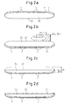
- Wafer cassettes 81A and 81B which store therein a plurality of wafers 20, are provided in the back-surface grinding unit 80. As shown in Figure 2a, a plurality of circuit patterns C are pre-formed on the front surface 21 of the wafer 20 that is supplied to the back-surface grinding unit 80, and a surface protection film 3 is stuck on to the front surface 21 to protect the circuit patterns C.
- each of the wafers 20 are taken out from the wafer cassettes 81A and 81B by robot arms 82A and 82B. Then, the wafer 20 is held, with its back surface 22 facing upward, by suction portions 84 of a rotary stage 83.
- grinding parts 85A and 85B of the back-surface grinding unit 80 are operated to grind the back surfaces 22 of the wafers 20.
- the thickness of the wafer 20 is reduced from the original wafer thickness LO to the after-grinding thickness LO'.
- the wafer 20 is conveyed by a robot arm 39 from the back-surface grinding unit 80 to the die attachment paste application unit 30.
- the die attachment paste application unit 30 a die attachment paste made of an adhesive paste material is applied to the ground back surface 22, so that a die attachment paste film 24 is thereby formed (see Figure 2d.)
- FIG 3 is a schematic diagram of the die attachment paste application unit according to the first embodiment of the present invention.
- the die attachment paste application unit 30 shown in Figure 3 is a spin-coat type application unit 30A. Note that the surface protection film 3 and the circuit patterns C have been omitted from Figures 3, 4 and 8.
- the die attachment paste application unit 30 comprises a holding table 33 that can be rotated by a motor 34, and a dispenser 32 that dispenses die attachment paste.
- the die attachment paste film 24 is thereby formed on the back surface 22 of the wafer 20. Then, the die attachment paste film 24 is subjected to a baking treatment.
- the die attachment paste can be applied in one operation to the entire back surface 22 of the wafer 20. Consequently, it is possible to apply the die attachment paste in a relatively shorter period of time than compared to a case where it is applied on individual chips after dicing.
- the thickness of the die attachment paste film 24 can be adjusted by changing the viscosity of the die attachment paste and/or the rotation speed of the table 33.
- the spin-coat type application unit 30A is utilized, the die attachment paste film 24 can be formed at the required thickness, even in cases where the thickness of the die attachment paste required is quite thin. For this reason, the spin-coat type application unit 30A is particularly advantageous in cases where the thickness of the die attachment paste required is quite thin.
- FIG 4 is a schematic diagram of the die attachment paste application unit according to the second embodiment of the present invention.
- the die attachment paste application unit 30 shown in Figure 4 is a screen-printing type application unit 30B.
- the movable squeegee 42 is arranged inside the frame body 41 so as to move along the inner walls of the frame body 41.
- the screen 44 having a hole 45 of a shape corresponding to the wafer 20, is provided on the lower surface of the frame body 41.
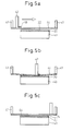
- Figures 5a to 5c are views for explaining the die attachment paste application unit according to the second embodiment of the present invention.
- the wafer 20 is held on the table 43, and the squeegee 42 is placed on one side in the frame body 41.
- a predetermined amount of the die attachment paste 49 is supplied to one side of the squeegee 42, directed to the direction of movement of the squeegee 42.
- the squeegee 42 is made to move on the screen 44 toward the other side of the frame body 41.
- the die attachment paste flows out from the hole 45 of the screen 44 and is applied little by little on the back surface 22 of the wafer 20.
- the die attachment paste film 24 is formed on the back surface 22 of the wafer 20. It should be evident that also in this embodiment, the die attachment paste can be applied in a relatively shorter period of time than compared to a case where it is applied on individual chips after dicing.
- a plurality of elongated holes 45a that are substantially parallel to each other and evenly spaced apart are formed in the first screen 44a. These holes 45a are formed so that as a whole they correspond to the external diameter of the wafer 20.
- a plurality of elongated holes 45b that are perpendicular to the holes 45a of the first screen 44a are formed in the second screen 44b similarly to the way the holes 45a are formed.
- the spaces between the plurality of holes 45a shown in Figure 6a and the spaces between the plurality of holes 45b shown in Figure 6b correspond substantially to the spaces between the circuit patterns C formed on the front surface 21 of the wafer 20. Therefore, the spaces between the plurality of holes 45a and the spaces between the plurality of holes 45b respectively correspond to the plurality of channels formed during the dicing process mentioned below.
- the table 43 is rotated so that the spaces between the circuit patterns C and the spaces between the holes of the first screen 44a are made to coincide, using a near-infrared ray camera (not shown) and a positioning pattern previously formed on the front surface 21 of the wafer 20.
- the screen-printing process of the first screen 44a is performed under the situation.
- the table 43 is rotated approximately 90 degrees, and the spaces between the circuit pattern C and the spaces between the holes of the second screen 44b are made to coincide.
- the screen-printing process of the second screen 44b is performed.
- the die attachment paste is applied to the back surface 22 of the wafer 20, except for the lattice-shaped parts.
- the lattice-shaped parts correspond to channels that are formed in the dicing process.
- the wafer 20 on which the die attachment paste film 24 has been formed is conveyed to the UV-irradiating unit 40.
- the UV-irradiating unit 40 a predefined quantity of UV is irradiated to the die attachment paste film 24.
- the die attachment paste film 24 thereby assumes the desired adhesion.
- the wafer 20 is conveyed to the dicing tape sticking unit 50, and the dicing tape 29 is stuck on the die attachment paste film 24 of the wafer 20 according to a known technique.
- the surface protection film 3 that is stuck on the top surface 21 of the wafer 20 is peeled off using a known technique, and then the wafer 20 is conveyed to the dicing unit 60 and diced.
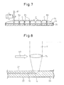
- Figure 7 is a side view of the wafer 20 as it is being diced.
- the wafer 20 is cut by the part of the dicing tape 29 by the dicing blade 61.
- the dicing blade 61 cuts the wafer 20 by moving along the lattice-shaped parts (see Figure 6c) on which the die attachment paste film 24 has not been formed. Consequently, the channels 65 formed by the dicing blade 61 correspond substantially to the aforementioned lattice-shaped parts. Due to the foregoing, the dicing blade 61 hardly cuts the die attachment paste film 24. Therefore, in the second embodiment, it is possible to prevent the dicing blade 61 from becoming clogged with the die attachment paste film 24, and the cutting ability of the dicing blade 61 from being reduced.
- channels (grooves) 65 are formed by the dicing blade 61 according to Figure 7, the channels 65 may be formed in other ways. Moreover, it is also possible to form the channels 65 by means of a laser dicing device.
- Figure 8 is a sectional side view for explaining laser dicing.
- the laser V from a laser source (not shown) is irradiated through a condensing lens 75 onto the front surface 21 of the wafer 20 under conditions where multiple photon absorption occurs.
- the light gathering point 74 is set to fall inside the wafer 20 rather close to the front surface 21.
- a modified area 74 is thereby formed in the vicinity of the light gathering point 74.
- the laser V and the condensing lens 75 are moved in accordance with the arrow X3, a band-like modified area 76 is formed inside the wafer 20.
- the laser V is made to pass through the wafer 20 and cause multiple photon absorption to occur inside the wafer. A modified area is thus formed. Consequently, the laser V is hardly absorbed by the front surface 21 of the wafer 20, and as a result, the front surface 21 of the wafer 20 does not melt, and cracks that deviate from the lines planned to be cut or the like do not occur on the top surface of the wafer.
- the modified area 76 is formed rather close to the front surface 21, when the modified area 76 breaks naturally in the thickness direction toward the front surface 21, the channels 65 corresponding to the width of the laser V are formed.
- the die attachment paste is applied, except for the lattice-shaped parts, there is no need to cut off the die attachment paste layer before or after the dicing, and consequently a laser dicing system can be utilized in the dicing unit 60.
- the wafer 20 is diced and divided into individual chips by the dicing operation shown in Figure 7 or Figure 8.
- the dicing tape 29 is expanded by means of a known technique, and, each chip is picked up from the dicing tape 29.
- the die attachment paste films 24, which serve as an adhesive on the bottom surfaces of the chips, the chips can then be die-bonded on to a lead frame or the like.
- the die attachment paste application unit 30 is arranged between the back-surface grinding unit 80 for the wafer 20 and the dicing unit 60.
- the invention provides for the die attachment paste to be applied in one operation on the entire ground back surface 22 of the wafer 20 in the die attachment paste application unit 30. For this reason, it is possible to apply die attachment paste in a shorter period of time than compared to a case where die attachment paste is separately applied to the individual chips after dicing.
- die attachment paste may be applied on the back surface 22 of the wafer 20 using a technique other than spin-coating or screen-printing, such as a so-called inkjet method. It should be understood that such cases also fall within the scope of the present invention.
Landscapes
- Die Bonding (AREA)
- Mechanical Treatment Of Semiconductor (AREA)
- Dicing (AREA)
- Container, Conveyance, Adherence, Positioning, Of Wafer (AREA)
Applications Claiming Priority (1)
| Application Number | Priority Date | Filing Date | Title |
|---|---|---|---|
| JP2006245645A JP2008066653A (ja) | 2006-09-11 | 2006-09-11 | ウェーハ処理方法およびウェーハ処理装置 |
Publications (1)
| Publication Number | Publication Date |
|---|---|
| EP1898459A2 true EP1898459A2 (de) | 2008-03-12 |
Family
ID=38698426
Family Applications (1)
| Application Number | Title | Priority Date | Filing Date |
|---|---|---|---|
| EP07116022A Withdrawn EP1898459A2 (de) | 2006-09-11 | 2007-09-10 | Waferverarbeitungsverfahren und Waferverarbeitungsvorrichtung |
Country Status (6)
| Country | Link |
|---|---|
| US (1) | US20080064188A1 (de) |
| EP (1) | EP1898459A2 (de) |
| JP (1) | JP2008066653A (de) |
| KR (1) | KR20080023666A (de) |
| SG (1) | SG141335A1 (de) |
| TW (1) | TW200830463A (de) |
Cited By (3)
| Publication number | Priority date | Publication date | Assignee | Title |
|---|---|---|---|---|
| WO2021225860A1 (en) * | 2020-05-07 | 2021-11-11 | Wolfspeed, Inc. | Packaged transistor with channeled die attach materials and process of implementing the same |
| US11424177B2 (en) | 2020-05-07 | 2022-08-23 | Wolfspeed, Inc. | Integrated circuit having die attach materials with channels and process of implementing the same |
| CN115410962A (zh) * | 2022-11-01 | 2022-11-29 | 四川九华光子通信技术有限公司 | 一种晶板蓝膜贴装装置 |
Families Citing this family (12)
| Publication number | Priority date | Publication date | Assignee | Title |
|---|---|---|---|---|
| JP5380886B2 (ja) * | 2007-04-18 | 2014-01-08 | 日立化成株式会社 | 接着剤付きウエハ及びその製造方法 |
| JP2010022990A (ja) * | 2008-07-24 | 2010-02-04 | Disco Abrasive Syst Ltd | 保護膜形成装置およびレーザー加工機 |
| JP5384972B2 (ja) * | 2009-03-02 | 2014-01-08 | 株式会社ディスコ | ウエーハの処理方法およびウエーハの処理装置 |
| JP5367421B2 (ja) * | 2009-03-16 | 2013-12-11 | 株式会社ディスコ | 接着剤層の形成方法及びウエーハの取り扱い方法 |
| JP5543739B2 (ja) * | 2009-08-06 | 2014-07-09 | 株式会社ボンマーク | メタルマスク及び半導体装置の製造方法 |
| JP2011040603A (ja) * | 2009-08-12 | 2011-02-24 | Disco Abrasive Syst Ltd | ウエーハの加工方法および研削装置 |
| JP2012033842A (ja) * | 2010-08-03 | 2012-02-16 | Disco Abrasive Syst Ltd | デバイスチップの製造方法 |
| JP2012043825A (ja) * | 2010-08-12 | 2012-03-01 | Disco Abrasive Syst Ltd | ウエーハの加工方法 |
| EP2671248A4 (de) * | 2011-02-01 | 2015-10-07 | Henkel Corp | Auf einem vorgeschnittenen wafer angebrachter unterfüllungsfilm auf einem dicing-tape |
| EP2671249A4 (de) | 2011-02-01 | 2015-10-07 | Henkel IP & Holding GmbH | Auf einem vorgeschnittenen wafer angebrachter unterfüllungsfilm |
| WO2013019499A2 (en) * | 2011-07-29 | 2013-02-07 | Henkel Corporation | Dicing before grinding after coating |
| KR102182856B1 (ko) * | 2020-03-11 | 2020-11-25 | 넥스타테크놀로지 주식회사 | 부품 실장 장치 |
Family Cites Families (7)
| Publication number | Priority date | Publication date | Assignee | Title |
|---|---|---|---|---|
| US5776799A (en) * | 1996-11-08 | 1998-07-07 | Samsung Electronics Co., Ltd. | Lead-on-chip type semiconductor chip package using an adhesive deposited on chip active surfaces at a wafer level and method for manufacturing same |
| US6676757B2 (en) * | 1999-12-17 | 2004-01-13 | Tokyo Electron Limited | Coating film forming apparatus and coating unit |
| JP2002100588A (ja) * | 2000-09-22 | 2002-04-05 | Shinkawa Ltd | 半導体装置の製造方法 |
| JP4471563B2 (ja) * | 2002-10-25 | 2010-06-02 | 株式会社ルネサステクノロジ | 半導体装置の製造方法 |
| US6916688B1 (en) * | 2002-12-05 | 2005-07-12 | National Semiconductor Corporation | Apparatus and method for a wafer level chip scale package heat sink |
| KR100517075B1 (ko) * | 2003-08-11 | 2005-09-26 | 삼성전자주식회사 | 반도체 소자 제조 방법 |
| US20050208700A1 (en) * | 2004-03-19 | 2005-09-22 | Chippac, Inc. | Die to substrate attach using printed adhesive |
-
2006
- 2006-09-11 JP JP2006245645A patent/JP2008066653A/ja active Pending
-
2007
- 2007-09-04 SG SG200706501-4A patent/SG141335A1/en unknown
- 2007-09-06 TW TW096133301A patent/TW200830463A/zh unknown
- 2007-09-07 US US11/852,132 patent/US20080064188A1/en not_active Abandoned
- 2007-09-10 EP EP07116022A patent/EP1898459A2/de not_active Withdrawn
- 2007-09-11 KR KR1020070092288A patent/KR20080023666A/ko not_active Ceased
Cited By (4)
| Publication number | Priority date | Publication date | Assignee | Title |
|---|---|---|---|---|
| WO2021225860A1 (en) * | 2020-05-07 | 2021-11-11 | Wolfspeed, Inc. | Packaged transistor with channeled die attach materials and process of implementing the same |
| US11424177B2 (en) | 2020-05-07 | 2022-08-23 | Wolfspeed, Inc. | Integrated circuit having die attach materials with channels and process of implementing the same |
| US11830810B2 (en) | 2020-05-07 | 2023-11-28 | Wolfspeed, Inc. | Packaged transistor having die attach materials with channels and process of implementing the same |
| CN115410962A (zh) * | 2022-11-01 | 2022-11-29 | 四川九华光子通信技术有限公司 | 一种晶板蓝膜贴装装置 |
Also Published As
| Publication number | Publication date |
|---|---|
| TW200830463A (en) | 2008-07-16 |
| JP2008066653A (ja) | 2008-03-21 |
| US20080064188A1 (en) | 2008-03-13 |
| KR20080023666A (ko) | 2008-03-14 |
| SG141335A1 (en) | 2008-04-28 |
Similar Documents
| Publication | Publication Date | Title |
|---|---|---|
| EP1898459A2 (de) | Waferverarbeitungsverfahren und Waferverarbeitungsvorrichtung | |
| JP5600035B2 (ja) | ウエーハの分割方法 | |
| JP5710133B2 (ja) | ワークの分割方法 | |
| CN107204286B (zh) | 晶片的加工方法 | |
| KR102210945B1 (ko) | 웨이퍼의 가공 방법 | |
| JP5959188B2 (ja) | ウエーハの加工方法 | |
| KR20160072775A (ko) | 웨이퍼의 가공 방법 | |
| JP2017092125A (ja) | ウエーハの加工方法 | |
| JP2017005158A (ja) | ウエーハの裏面研削方法 | |
| CN102848305B (zh) | 被加工物的磨削方法 | |
| CN102157449A (zh) | 晶片的加工方法 | |
| KR102631710B1 (ko) | 웨이퍼의 가공 방법 | |
| JP2018125479A (ja) | ウェーハの加工方法 | |
| US10199253B2 (en) | Method for manufacturing semiconductor devices through peeling using UV-ray | |
| JP5885396B2 (ja) | デバイスチップの製造方法 | |
| JP2012084720A (ja) | ワークの加工方法 | |
| KR20160075326A (ko) | 웨이퍼의 가공 방법 | |
| CN111293069B (zh) | 器件芯片的制造方法 | |
| JP6842311B2 (ja) | ウェーハの加工方法 | |
| JP6071702B2 (ja) | ウエーハの加工方法 | |
| JP4554384B2 (ja) | ウェーハの分割方法 | |
| JP2005260154A (ja) | チップ製造方法 | |
| JP6692580B2 (ja) | デバイスチップ及びその製造方法 | |
| JP4681704B2 (ja) | 半導体ウェーハの分割方法 | |
| TWI267913B (en) | Wafer dicing method |
Legal Events
| Date | Code | Title | Description |
|---|---|---|---|
| PUAI | Public reference made under article 153(3) epc to a published international application that has entered the european phase |
Free format text: ORIGINAL CODE: 0009012 |
|
| 17P | Request for examination filed |
Effective date: 20071001 |
|
| AK | Designated contracting states |
Kind code of ref document: A2 Designated state(s): AT BE BG CH CY CZ DE DK EE ES FI FR GB GR HU IE IS IT LI LT LU LV MC MT NL PL PT RO SE SI SK TR |
|
| AX | Request for extension of the european patent |
Extension state: AL BA HR MK YU |
|
| STAA | Information on the status of an ep patent application or granted ep patent |
Free format text: STATUS: THE APPLICATION HAS BEEN WITHDRAWN |
|
| 18W | Application withdrawn |
Effective date: 20081021 |