EP1880197B1 - Microfluidic device for use with a compact optical detection system - Google Patents
Microfluidic device for use with a compact optical detection system Download PDFInfo
- Publication number
- EP1880197B1 EP1880197B1 EP06769836.5A EP06769836A EP1880197B1 EP 1880197 B1 EP1880197 B1 EP 1880197B1 EP 06769836 A EP06769836 A EP 06769836A EP 1880197 B1 EP1880197 B1 EP 1880197B1
- Authority
- EP
- European Patent Office
- Prior art keywords
- channels
- optical detection
- detection system
- alignment marks
- microfluidic device
- Prior art date
- Legal status (The legal status is an assumption and is not a legal conclusion. Google has not performed a legal analysis and makes no representation as to the accuracy of the status listed.)
- Active
Links
Images


Classifications
-
- G—PHYSICS
- G01—MEASURING; TESTING
- G01B—MEASURING LENGTH, THICKNESS OR SIMILAR LINEAR DIMENSIONS; MEASURING ANGLES; MEASURING AREAS; MEASURING IRREGULARITIES OF SURFACES OR CONTOURS
- G01B11/00—Measuring arrangements characterised by the use of optical techniques
- G01B11/002—Measuring arrangements characterised by the use of optical techniques for measuring two or more coordinates
-
- B—PERFORMING OPERATIONS; TRANSPORTING
- B01—PHYSICAL OR CHEMICAL PROCESSES OR APPARATUS IN GENERAL
- B01L—CHEMICAL OR PHYSICAL LABORATORY APPARATUS FOR GENERAL USE
- B01L3/00—Containers or dishes for laboratory use, e.g. laboratory glassware; Droppers
- B01L3/50—Containers for the purpose of retaining a material to be analysed, e.g. test tubes
- B01L3/502—Containers for the purpose of retaining a material to be analysed, e.g. test tubes with fluid transport, e.g. in multi-compartment structures
- B01L3/5027—Containers for the purpose of retaining a material to be analysed, e.g. test tubes with fluid transport, e.g. in multi-compartment structures by integrated microfluidic structures, i.e. dimensions of channels and chambers are such that surface tension forces are important, e.g. lab-on-a-chip
- B01L3/502715—Containers for the purpose of retaining a material to be analysed, e.g. test tubes with fluid transport, e.g. in multi-compartment structures by integrated microfluidic structures, i.e. dimensions of channels and chambers are such that surface tension forces are important, e.g. lab-on-a-chip characterised by interfacing components, e.g. fluidic, electrical, optical or mechanical interfaces
-
- G—PHYSICS
- G01—MEASURING; TESTING
- G01N—INVESTIGATING OR ANALYSING MATERIALS BY DETERMINING THEIR CHEMICAL OR PHYSICAL PROPERTIES
- G01N21/00—Investigating or analysing materials by the use of optical means, i.e. using sub-millimetre waves, infrared, visible or ultraviolet light
- G01N21/62—Systems in which the material investigated is excited whereby it emits light or causes a change in wavelength of the incident light
- G01N21/63—Systems in which the material investigated is excited whereby it emits light or causes a change in wavelength of the incident light optically excited
- G01N21/64—Fluorescence; Phosphorescence
- G01N21/645—Specially adapted constructive features of fluorimeters
-
- B—PERFORMING OPERATIONS; TRANSPORTING
- B01—PHYSICAL OR CHEMICAL PROCESSES OR APPARATUS IN GENERAL
- B01L—CHEMICAL OR PHYSICAL LABORATORY APPARATUS FOR GENERAL USE
- B01L2200/00—Solutions for specific problems relating to chemical or physical laboratory apparatus
- B01L2200/02—Adapting objects or devices to another
- B01L2200/025—Align devices or objects to ensure defined positions relative to each other
-
- B—PERFORMING OPERATIONS; TRANSPORTING
- B01—PHYSICAL OR CHEMICAL PROCESSES OR APPARATUS IN GENERAL
- B01L—CHEMICAL OR PHYSICAL LABORATORY APPARATUS FOR GENERAL USE
- B01L2300/00—Additional constructional details
- B01L2300/08—Geometry, shape and general structure
- B01L2300/0809—Geometry, shape and general structure rectangular shaped
- B01L2300/0816—Cards, e.g. flat sample carriers usually with flow in two horizontal directions
-
- B—PERFORMING OPERATIONS; TRANSPORTING
- B01—PHYSICAL OR CHEMICAL PROCESSES OR APPARATUS IN GENERAL
- B01L—CHEMICAL OR PHYSICAL LABORATORY APPARATUS FOR GENERAL USE
- B01L3/00—Containers or dishes for laboratory use, e.g. laboratory glassware; Droppers
- B01L3/50—Containers for the purpose of retaining a material to be analysed, e.g. test tubes
- B01L3/502—Containers for the purpose of retaining a material to be analysed, e.g. test tubes with fluid transport, e.g. in multi-compartment structures
- B01L3/5027—Containers for the purpose of retaining a material to be analysed, e.g. test tubes with fluid transport, e.g. in multi-compartment structures by integrated microfluidic structures, i.e. dimensions of channels and chambers are such that surface tension forces are important, e.g. lab-on-a-chip
-
- G—PHYSICS
- G01—MEASURING; TESTING
- G01N—INVESTIGATING OR ANALYSING MATERIALS BY DETERMINING THEIR CHEMICAL OR PHYSICAL PROPERTIES
- G01N21/00—Investigating or analysing materials by the use of optical means, i.e. using sub-millimetre waves, infrared, visible or ultraviolet light
- G01N21/01—Arrangements or apparatus for facilitating the optical investigation
- G01N2021/0162—Arrangements or apparatus for facilitating the optical investigation using microprocessors for control of a sequence of operations, e.g. test, powering, switching, processing
-
- G—PHYSICS
- G01—MEASURING; TESTING
- G01N—INVESTIGATING OR ANALYSING MATERIALS BY DETERMINING THEIR CHEMICAL OR PHYSICAL PROPERTIES
- G01N21/00—Investigating or analysing materials by the use of optical means, i.e. using sub-millimetre waves, infrared, visible or ultraviolet light
- G01N21/62—Systems in which the material investigated is excited whereby it emits light or causes a change in wavelength of the incident light
- G01N21/63—Systems in which the material investigated is excited whereby it emits light or causes a change in wavelength of the incident light optically excited
- G01N21/64—Fluorescence; Phosphorescence
- G01N2021/6417—Spectrofluorimetric devices
- G01N2021/6419—Excitation at two or more wavelengths
-
- G—PHYSICS
- G01—MEASURING; TESTING
- G01N—INVESTIGATING OR ANALYSING MATERIALS BY DETERMINING THEIR CHEMICAL OR PHYSICAL PROPERTIES
- G01N21/00—Investigating or analysing materials by the use of optical means, i.e. using sub-millimetre waves, infrared, visible or ultraviolet light
- G01N21/62—Systems in which the material investigated is excited whereby it emits light or causes a change in wavelength of the incident light
- G01N21/63—Systems in which the material investigated is excited whereby it emits light or causes a change in wavelength of the incident light optically excited
- G01N21/64—Fluorescence; Phosphorescence
- G01N2021/6417—Spectrofluorimetric devices
- G01N2021/6421—Measuring at two or more wavelengths
-
- G—PHYSICS
- G01—MEASURING; TESTING
- G01N—INVESTIGATING OR ANALYSING MATERIALS BY DETERMINING THEIR CHEMICAL OR PHYSICAL PROPERTIES
- G01N21/00—Investigating or analysing materials by the use of optical means, i.e. using sub-millimetre waves, infrared, visible or ultraviolet light
- G01N21/62—Systems in which the material investigated is excited whereby it emits light or causes a change in wavelength of the incident light
- G01N21/63—Systems in which the material investigated is excited whereby it emits light or causes a change in wavelength of the incident light optically excited
- G01N21/64—Fluorescence; Phosphorescence
- G01N21/645—Specially adapted constructive features of fluorimeters
- G01N2021/6463—Optics
- G01N2021/6478—Special lenses
-
- G—PHYSICS
- G01—MEASURING; TESTING
- G01N—INVESTIGATING OR ANALYSING MATERIALS BY DETERMINING THEIR CHEMICAL OR PHYSICAL PROPERTIES
- G01N2201/00—Features of devices classified in G01N21/00
- G01N2201/06—Illumination; Optics
- G01N2201/062—LED's
- G01N2201/0627—Use of several LED's for spectral resolution
-
- G—PHYSICS
- G02—OPTICS
- G02B—OPTICAL ELEMENTS, SYSTEMS OR APPARATUS
- G02B21/00—Microscopes
- G02B21/16—Microscopes adapted for ultraviolet illumination ; Fluorescence microscopes
Definitions
- This invention relates generally to the field of detection optics. More specifically, the invention relates to a microfluidic device compatible with a compact optical detection system for detecting fluorescent signals.
- optical detection systems for microfluidic devices are large, expensive, and inflexible.
- the optical detection system is the costliest subsystem.
- the size, expense, and rigidity of current optical detection systems result largely from such systems employing multiple high quality lasers for fluorescence excitation, along with multiple charge-coupled device (CCD) cameras for detection.
- CCD charge-coupled device
- Alignment and focusing of existing optical detection systems also presents problems.
- optics are aligned and focused by viewing fluorescent dye flowing through a channel in a microfluidic device.
- the dye must be allowed to reach the detection region of the microfluidic device before performing the alignment and focusing process. This can take several minutes for some microfluidic devices.
- the fluorescent dye is typically flushed out of the channel after focusing, a time-consuming and sometimes difficult process.
- the dye can be expensive and unstable, adding to the cost and complexity of the process.
- US 2002/0015147 describes methods and apparatus for locating a capillary channel in a lab chip by scanning channels with a light source and monitoring the resulting light at the edges of the lab chip.
- the methods and apparatus use channels in the chip which have at least partially sloped side walls.
- One aspect of the present invention is a dry-focus microfluidic device as defined in claim 1.
- the device comprises a first substrate; multiple channels formed in the first substrate, at least one of which is a microfluidic channel; multiple optical alignment marks having curved walls that are formed in the first substrate spaced apart from the channels; and a second substrate bonded to the first substrate to form covered channels and closed optical alignment marks. At least one of the channels is positioned between at least two of the optical alignment marks.
- the system comprises a light-emitting diode (LED); means for collimating the light emitted by the LED; an aspherical, fused-silica objective lens; means for directing the collimated light through the objective lens onto the microfluidic device; and means for detecting a fluorescent signal emitted from the microfluidic device.
- the system may include a second, external light source, which may be either an LED or a laser.
- the working distance from the objective lens to the microfluidic device may be sized to permit light from the LED or laser to be brought in along a diagonal path to illuminate the microfluidic device.
- microfluidic is used herein to define chambers and flow passages having cross-sectional dimensions on the order of 0,1 ⁇ m to 500 ⁇ m.
- the microfluidic flow channels and fluid handling regions have preferred depths on the order of 0.1 ⁇ m to 100 ⁇ m, typically 2,0 ⁇ m to 50 ⁇ m.
- the channels have preferred widths on the order of 2.0 ⁇ m to 500 ⁇ m, more preferably 3.0 ⁇ m to 100 ⁇ m. For many applications, channels of 5.0 ⁇ m to 50 ⁇ m widths will be useful. Chambers in the device often will have larger dimensions, e.g., a few millimeters.
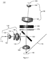
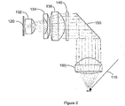
- system 100 comprises an LED light source 110 ; a slit 120 ; a slit lens 130 comprising three slit lens elements 132 , 134 , and 136; an excitation bandpass filter 140 ; a beam splitter 150 , an objective lens 160 ; a rejection filter 170 ; a diffraction grating 180 ; a CCD lens 190 comprising CCD lens elements 192 and 194 ; and a CCD array 196 .
- a second light source which may be either a laser or an LED, is indicated at 115 .
- a microfluidic device is indicated at 165 .
- Slit 120 is back illuminated by LED 110 .
- the LED may be used in place of or in addition to a laser light source, as will be explained below.
- the size, shape, wavelength, and power level of the LED may be varied. LEDs are currently available in various colors, including UV, blue, cyan, and green, representing emission wavelengths of 400-750 nm. Multiple LEDs may be loaded into the system, e.g., placed in a rotating turret having a motorized mechanism, and selected for the fluorophore being detected.
- the spectral resolution of the present embodiment is inversely proportional to the sensitivity, as is the case for any spectrometer. Therefore, placing a wider slit results in higher sensitivity but poorer color separation. For many assays, only two or three color bands may be required, thus allowing the slit to be set wider for high sensitivity.
- slit lens 130 After passing through slit 120 , light from LED 110 is collected and collimated by slit lens 130 , which compensates for axial color introduced at objective lens 160 as light travels through it toward device 165 .
- the color corrector lenses are necessary to prevent the image of the slit cast upon the microfluidic device for excitation from becoming smeared out, causing a loss of spatial resolution. Color may be corrected for more than one wavelength range, in the present example 350-400 nm and 430-480 nm.
- the slit-to-lens distance is set differently for each range, for example through software controls available to the user.
- Slit lens 130 comprises slit lens elements 132 , 134 , and 136 .
- each lens element is custom designed and made from a UV-transparent, dispersive glass.
- Slit lens 130 is designed for UV wavelengths emitted by UV LEDs. It works with objective lens 160 to form a sharp image of slit 120 on microfluidic device 165 .
- Slit lens element 132 is made from Hoya glass type TAC6, and has an edge diameter of 14 mm and a center thickness of 10.9 mm.
- Slit lens element 134 is made from Hoya glass type NBFD12, and has a diameter of 23 mm and a center thickness of 3.14 mm.
- Slit lens element 136 is made of fused silica and is a duplicate of objective lens 160 , which is described fully below.
- Excitation bandpass filter 140 attenuates frequencies outside the desired range before flat, dichroic beam splitter 150 (e.g., a dichroic mirror) directs the now collimated excitation light emitted by LED 110 down through objective lens 160 onto microfluidic device 165 .
- dichroic beam splitter 150 e.g., a dichroic mirror
- the full excitation optical path is illustrated in FIG. 2 .
- Objective lens 160 is a high efficiency, custom-designed, fused-silica objective of 0.5 numerical aperture (NA), with a 60-degree total cone angle of collected light. As can be seen in FIG. 1 , the objective must not only deliver excitation light, but also collect and collimate fluorescent light. Light collection efficiency goes approximately as the square of NA. The high collection efficiency of objective lens 160 enables the use of lower power, and hence less expensive, light sources such as LED 110 .
- NA numerical aperture
- Objective lens 160 is a single element of fused silica to reduce unwanted background fluorescence, which would limit assay sensitivity because the lens is used in epifluorescence mode. Because the lens is made of a single material with finite dispersion, its focal length is a slight function of wavelength. The lens has an edge diameter of 27 mm and a thickness of 15.02 mm. The edges of the lens are beveled at 45 degrees to an 0.5 mm maximum face width. The back surface of the lens is aspherical to correct spherical aberration. The system's aperture stop is located on the backside of the lens, with no vignetting from there to the CCD array.
- Objective lens 160 was optimized at a single wavelength (550 nm) by modeling it with a paraxial lens with the image at the paraxial focus.
- the object plane was modeled to lie below 700 micrometers of a parallel plate made of fused silica, i.e., the top of the microfluidic device.
- the objective was optimized to form an image at infinity. All object field points were weighted equally.
- the working distance from objective lens 160 to microfluidic device 165 is 16 mm.
- the objective's diameter (27 mm) and working distance allow clearance for external laser beam illumination brought in at, for example, a. 45-degree angle.
- a variety of lasers can be used in conjunction with embodiments of the optical detection systems.
- a blue LED may be coupled with a red laser.
- One LED and one or more laser beams brought in collinearly can be used at the same time.
- light from a second LED may also be brought in externally along a diagonal path for alignment and focusing purposes.
- Light source 115 represents either a laser or an LED light source.
- the working distance from objective lens 160 to microfluidic device 165 also offers a wide (3.4-mm) field of view, allowing fluorescence measurement in up to 16 channels pitched at 200 micrometers or 20 channels pitched at 150 micrometers.
- System 100 accommodates emission wavelengths ranging between 400 nm and 750 nm.
- the fluorescent signal(s) emitted from microfluidic device 165 pass through dichroic mirror 150 with minimal reflection.
- Rejection filter 170 prevents excitation light from being transmitted along the detection path.
- diffraction grating 180 which is an anti-reflection coated BK7 blazed diffraction grating used for dispersing the fluorescent light into its constituent colors so they can be detected independently.
- the grating blaze angle is chosen to optimize the transmission of visible light into the first order.
- the zero th and second orders are, preferably, not cast onto CCD array 196 .
- objective lens 160 Because objective lens 160 is a singlet, it introduces chromatic aberrations, primarily in the form of axial color. These aberrations are corrected at CCD lenses 192 and 194 .
- the axial color is also partly corrected by tilting CCD array 196 as well as CCD lenses 192 and 194 .
- the rotation angle is restricted to less than 15 degrees off-normal. Tilting CCD array 196 corrects the axial colors because the colors are spread across the CCD array with diffraction grating 180 .
- CCD lens 190 comprises CCD lens elements 192 and 194 .
- Lens element 192 is a field lens with an edge diameter of 16.5 mm and a thickness of 7.63 mm.
- CCD lens element 194 is a triplet of various glasses chosen for their dispersive properties. The CCD lenses need not be made of low fluorescence glass because excitation light does not pass through them.
- CCD lens 194 has an overall edge diameter of 40 mm and thicknesses of 14.0 mm, 2.5 mm, and 2.5 mm for the three portions of the lens.
- CCD array 196 serves as a detector.
- the format of the array is 658 ⁇ 496 pixels, with 7.4 micrometer pixel size. Pixel grouping is programmable through a software interface.
- the detection bands typically correspond to the location of channels on microfluidic device 165.
- the present embodiment was designed to induce and read fluorescence from up to 16 channels pitched 200 micrometers apart or 20 channels pitched 150 micrometers apart.
- the detection bands employed by the detector can be aligned with the channels using techniques described below.
- the detector output will be a two-dimensional array with the channels forming one axis of the array, while the detected colors form the other axis.
- a system designed to detect green and red fluorescence emanating from 12 channels in a microfluidic device would output a 12 ⁇ 2 array.
- optical detection system may be varied in numerous ways.
- design parameters of the lenses used in the system may be varied, including diameter, numerical aperture, focal length, and material, with the exception that the objective lens is preferably fused silica.
- Light sources may also vary, with different combinations of CCD and laser light sources being used.
- the format of the CCD array may vary as well.
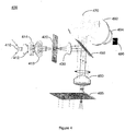
- FIG. 4 illustrates an alternative and even less expensive embodiment that is not multispectral.
- System 400 comprises an LED light source 410 , condenser lenses 412 and 413 separated by an excitation bandpass filter 414 , a slit 420 , a single slit lens 430 , a beam splitter 450 , custom-designed high-numerical-aperture objective lens 460 , a folding mirror 470 , and a CCD lens 492 separated from a CCD array 496 by an emission bandpass filter 494 .
- the working distance between objective lens 460 and the microfluidic device, shown at 465 in FIG. 4 is similar to that in the previous example, allowing the system to be used with a laser as well as an LED. Both excitation and detection optical paths are shown in FIG. 4 .
- LED light source 410 is a blue LED (e.g., a Cree XLamp 7090 LED).
- Condenser lens 412 is a 15-mm diameter lens with an effective focal length of 12 mm, fabricated using B270 glass with a single-layer MgF 2 coating (e.g., from Newport Corp.). Lens 412 has an effective focal length of 12 mm.
- Condenser lens 413 is a 25-mm diameter lens fabricated using BK7 glass with a 1 ⁇ 4-wave MgF 2 coating (e.g., from Edmund Optics). Lens 413 has an effective focal length of 30 mm.
- Excitation bandpass filter 414 is fabricated from NBK7 glass to have a center wavelength of 470 nm, a diameter of 25 mm, and a thickness of 5 mm (e.g., from Semrock).
- Slit 420 is a 500-micrometer chromium-coated soda lime glass slit with a diameter of 25.4 mm and a thickness of 1.5 mm (e.g., from Lenox Laser).
- Slit lens 430 is an 18-mm diameter lens with an effective focal length of 27 mm, fabricated using SF5 glass with a 1 ⁇ 4-wave MgF 2 coating (e.g., from Edmund Optics).
- Beam splitter 450 is an extended-band dichroic beam splitter (e.g., from Semrock).
- Objective lens 460 is the custom-designed, high-numerical-aperture objective lens that is also illustrated at 160 and was described previously.
- Folding mirror 470 is a standard, commercially available folding mirror.
- CCD lens 492 is, e.g., a Nikon 50-mm f1.4 lens used with a Rolera-XR CCD camera, i.e., CCD array 496 .
- Emission bandpass filter 494 is fabricated from NBK7 glass to have a center wavelength of 531 nm, a diameter of 25 mm, and a thickness of 5 mm (e.g., from Semrock).
- the optical detection system offers a number of advantages over existing systems.
- the lens layout allows excitation light to be delivered both axially, as in epifluorescence systems, or externally at an oblique angle.
- the high numerical aperture of the custom, fused-silica objective lens permits the use of a lower power and less expensive light source in the form of an LED. For example, a blue LED costs about $25, while a blue laser costs about $10,000.
- the lens system also allows the use of a single CCD, rather than multiple CCDs, for additional cost savings. In addition to being less expensive than typical optical detection systems, the described system is more compact. Because of the low cost and small size of systems in accordance with the invention, several LEDs of various colors may be incorporated into a system such as that seen in FIG. 1 , thus providing built-in flexibility of excitation colors. Detection wavelengths may be set through software controls available to the user.
- optical detection system Another advantage of the optical detection system is that light from a second LED can be delivered externally at an oblique angle to the microfluidic device for alignment and focusing purposes.
- an optical detection system such as has been described above may be combined with a dry-focus microfluidic device of the present invention to form an analytical unit.
- microfluidic device in accordance with the present invention, is illustrated at 500 in FIG. 5 .
- the number and arrangement of chambers and flow passages may vary, depending on the intended use for the device.
- At least one channel of the dry-focus device is microfluidic.
- a detection region 515 of FIG. 5 is seen enlarged in FIG. 6 . While detection region 515 includes 12 channels and a total of 22 optical alignment marks arranged in two arrays positioned parallel to and to the outside of the channels, 11 marks per array, the number of channels shown in FIG. 6 has been reduced to four to allow better visualization of the individual elements.
- the spacing 611 between channels 610 i.e., the channel pitch
- the spacing 621 between marks 620 is 100 micrometers.
- the distance between marks 620 and an adjacent channel 610 , indicated at 622 is at least 20 micrometers, regardless of the number and pitch of the channels.
- Nominal illumination length 630 is 500 micrometers.
- the nominal detection center is shown at 640 .
- Channels are typically etched into a substrate using standard photolithographic methods known in the art. Alignment marks are also etched into the substrate and may be the same depth as the channels.
- marks 620 are formed using a square, 10 ⁇ 10 micrometer mask feature, resulting in an alignment mark somewhat larger than the mask feature.
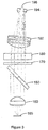
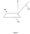
- An isotropic etch is used in fabricating alignment marks 620 , resulting in a mark with a flat base and curved walls. See, for example, FIG. 7 , which shows a cross-sectional view of an individual alignment mark 620 .
- a second substrate or cover 625 is bonded to the etched substrate, forming covered channels 610 and closed optical alignment marks 620 .
- a white LED is used to illuminate alignment marks 620 .
- Light 615 from the LED is brought in externally along a diagonal path.
- an optical detection system such as has been described above is configured with the objective lens spaced above the device to allow for this diagonal path.
- the microfluidic device is positioned for illumination and detection with the base of the alignment mark nearest the optics.
- Light 615 from the white LED reflects off the curved wall at an angle that directs the light into the objective lens of the optical detection system. Because the device surfaces are virtually flat, light delivered at an oblique angle is not reflected from these surfaces into the objective lens.
- Channels etched at the same time as the alignment marks and, therefore, having the same curve, are virtually invisible because they are filled with a liquid, which allows light to pass through the channel wall rather than being reflected off the curved wall.
- microfluidic devices are typically primed with a buffer or other liquid prior to use.
- FIG. 8A shows an optical signal such as would be generated by the two arrays of alignment marks that are described above and illustrated in FIG. 6 .
- each array produces a distinct peak 810.
- an array may include any number of alignment marks, one skilled in the art will appreciate that the use of multiple alignment marks is preferable in order to produce a peak that is easily distinguished from a peak produced by a speck of dust or other small defect on or in the microfluidic device.
- FIG. 8B shows alignment marks 810 as well as a peak 815 produced by a defect on or in the device. As can be seen, peaks produced by the arrays of alignment marks 810 are significantly higher than the peak 815 produced by the defect.
- an autofocus algorithm may simply search for the two highest peaks. Because the autofocus algorithm has been provided data regarding the distance between the two arrays of alignment marks as well as the distance from each array to the adjacent channel and the pitch of the channels, the optical detection system can be focused and aligned to the alignment marks and then displaced the appropriate distance to align to a microfluidic channel. Thus, the autofocus algorithm can be made robust against defects by rejecting small peaks and by verifying spacing between expected peaks.
- microfluidic device in accordance with the present invention may be varied in numerous ways, without departing from the scope of the appended claims.
- embodiments of the invention could be employed for single-channel as well as multichannel microfluidic devices.
- Control of the alignment and focusing could be manual rather than being automatically controlled by an autofocus algorithm.
- the number of marks may be varied.
- the shape of the marks may be varied as well; however, the shape and size were optimized for the embodiment described above.
- the depth of the marks is not critical and may be varied.
- the exact location along the direction parallel to the channels is also not critical. Placement of the marks with relation to the channels may vary as well, provided the marks are not positioned so close to the channels that the integrity of the channels is put at risk.
- a number of different wavelengths of light could be used to illuminate the optical alignment marks.
- a solid-state fluorescent material could be placed within the optical alignment marks to increase the optical signal produced by the marks.
- FIG. 9 shows an alternative embodiment having a pattern in which alignment marks 910 are positioned between each of four channels 920 as well as outside each outer channel. Each of the four channels branches into three channels in the top half of the figure.
- the screen capture shown in FIG. 10 comprises line mode data obtained from a CCD array such as has been described above. When the five peaks produced by reflection of light from alignment marks 910 are centered on the CCD line mode data from the optical detection system, the white bands are positioned correctly to sense fluorescent signals from channels 920 on the dry-focus microfluidic device.
- a method for aligning and focusing an optical detection system is also described.
- a microfluidic device having a plurality of channels and a plurality of optical alignment marks is provided. At least one of the channels is microfluidic.
- the optical alignment marks were formed by etching the marks into a substrate using an isotropic etch and a square, 10 ⁇ 10 micrometer mask feature.
- the device is positioned relative to the optics of the optical detection system with the bottoms of the optical alignment marks nearer to the optics than are the tops of the marks.
- the light from an external white LED is brought in at an oblique angle to illuminate the optical alignment marks.
- Data collection for the optical detection system is set to line mode.
- the system is aligned using light reflected from the optical alignment marks.
- Embodiments of the invention offer a number of advantages over previously known apparatuses.
- One advantage is that the invention does not require flowing dye through channels to perform optical alignment and focusing. Not flowing dye eliminates the use of expensive and unstable dyes, removes the need to wait for dye breakthrough, and removes the need to flush out dye after alignment and focusing.
Landscapes
- Chemical & Material Sciences (AREA)
- Health & Medical Sciences (AREA)
- General Health & Medical Sciences (AREA)
- General Physics & Mathematics (AREA)
- Physics & Mathematics (AREA)
- Analytical Chemistry (AREA)
- Clinical Laboratory Science (AREA)
- Hematology (AREA)
- Dispersion Chemistry (AREA)
- Chemical Kinetics & Catalysis (AREA)
- Nuclear Medicine, Radiotherapy & Molecular Imaging (AREA)
- Life Sciences & Earth Sciences (AREA)
- Biochemistry (AREA)
- Immunology (AREA)
- Pathology (AREA)
- Investigating, Analyzing Materials By Fluorescence Or Luminescence (AREA)
- Optical Measuring Cells (AREA)
Priority Applications (1)
| Application Number | Priority Date | Filing Date | Title |
|---|---|---|---|
| EP11190622.8A EP2453223B1 (en) | 2005-04-12 | 2006-04-12 | Optical detection system for a microfluidic device and method for aligning and focusing an optical detection system |
Applications Claiming Priority (2)
| Application Number | Priority Date | Filing Date | Title |
|---|---|---|---|
| US67073605P | 2005-04-12 | 2005-04-12 | |
| PCT/US2006/014313 WO2006115863A2 (en) | 2005-04-12 | 2006-04-12 | Compact optical detection system for microfluidic devices |
Related Child Applications (2)
| Application Number | Title | Priority Date | Filing Date |
|---|---|---|---|
| EP11190622.8A Division-Into EP2453223B1 (en) | 2005-04-12 | 2006-04-12 | Optical detection system for a microfluidic device and method for aligning and focusing an optical detection system |
| EP11190622.8A Division EP2453223B1 (en) | 2005-04-12 | 2006-04-12 | Optical detection system for a microfluidic device and method for aligning and focusing an optical detection system |
Publications (2)
| Publication Number | Publication Date |
|---|---|
| EP1880197A2 EP1880197A2 (en) | 2008-01-23 |
| EP1880197B1 true EP1880197B1 (en) | 2019-06-12 |
Family
ID=37215227
Family Applications (2)
| Application Number | Title | Priority Date | Filing Date |
|---|---|---|---|
| EP06769836.5A Active EP1880197B1 (en) | 2005-04-12 | 2006-04-12 | Microfluidic device for use with a compact optical detection system |
| EP11190622.8A Active EP2453223B1 (en) | 2005-04-12 | 2006-04-12 | Optical detection system for a microfluidic device and method for aligning and focusing an optical detection system |
Family Applications After (1)
| Application Number | Title | Priority Date | Filing Date |
|---|---|---|---|
| EP11190622.8A Active EP2453223B1 (en) | 2005-04-12 | 2006-04-12 | Optical detection system for a microfluidic device and method for aligning and focusing an optical detection system |
Country Status (7)
Families Citing this family (76)
| Publication number | Priority date | Publication date | Assignee | Title |
|---|---|---|---|---|
| US6048734A (en) | 1995-09-15 | 2000-04-11 | The Regents Of The University Of Michigan | Thermal microvalves in a fluid flow method |
| US6692700B2 (en) | 2001-02-14 | 2004-02-17 | Handylab, Inc. | Heat-reduction methods and systems related to microfluidic devices |
| US7323140B2 (en) | 2001-03-28 | 2008-01-29 | Handylab, Inc. | Moving microdroplets in a microfluidic device |
| US7829025B2 (en) | 2001-03-28 | 2010-11-09 | Venture Lending & Leasing Iv, Inc. | Systems and methods for thermal actuation of microfluidic devices |
| EP3718635A1 (en) | 2003-07-31 | 2020-10-07 | Handylab, Inc. | Processing particle-containing samples |
| US8852862B2 (en) | 2004-05-03 | 2014-10-07 | Handylab, Inc. | Method for processing polynucleotide-containing samples |
| US7998708B2 (en) | 2006-03-24 | 2011-08-16 | Handylab, Inc. | Microfluidic system for amplifying and detecting polynucleotides in parallel |
| US11806718B2 (en) | 2006-03-24 | 2023-11-07 | Handylab, Inc. | Fluorescence detector for microfluidic diagnostic system |
| WO2007112114A2 (en) | 2006-03-24 | 2007-10-04 | Handylab, Inc. | Integrated system for processing microfluidic samples, and method of using same |
| US10900066B2 (en) | 2006-03-24 | 2021-01-26 | Handylab, Inc. | Microfluidic system for amplifying and detecting polynucleotides in parallel |
| US8656949B2 (en) | 2006-08-15 | 2014-02-25 | University Of Maryland College Park | Microfluidic devices and methods of fabrication |
| WO2008060604A2 (en) | 2006-11-14 | 2008-05-22 | Handylab, Inc. | Microfluidic system for amplifying and detecting polynucleotides in parallel |
| WO2008061165A2 (en) | 2006-11-14 | 2008-05-22 | Handylab, Inc. | Microfluidic cartridge and method of making same |
| KR101334183B1 (ko) | 2007-06-01 | 2013-12-02 | 삼성전자주식회사 | 미세 반응을 위한 형광 검출 모듈과 이를 구비한 형광 검출시스템 |
| US8133671B2 (en) | 2007-07-13 | 2012-03-13 | Handylab, Inc. | Integrated apparatus for performing nucleic acid extraction and diagnostic testing on multiple biological samples |
| USD621060S1 (en) | 2008-07-14 | 2010-08-03 | Handylab, Inc. | Microfluidic cartridge |
| US8105783B2 (en) | 2007-07-13 | 2012-01-31 | Handylab, Inc. | Microfluidic cartridge |
| CA2693654C (en) | 2007-07-13 | 2018-02-13 | Handylab, Inc. | Polynucleotide capture materials, and methods of using same |
| US9186677B2 (en) | 2007-07-13 | 2015-11-17 | Handylab, Inc. | Integrated apparatus for performing nucleic acid extraction and diagnostic testing on multiple biological samples |
| US8287820B2 (en) | 2007-07-13 | 2012-10-16 | Handylab, Inc. | Automated pipetting apparatus having a combined liquid pump and pipette head system |
| US8182763B2 (en) | 2007-07-13 | 2012-05-22 | Handylab, Inc. | Rack for sample tubes and reagent holders |
| US9618139B2 (en) | 2007-07-13 | 2017-04-11 | Handylab, Inc. | Integrated heater and magnetic separator |
| US20090136385A1 (en) | 2007-07-13 | 2009-05-28 | Handylab, Inc. | Reagent Tube |
| US8016260B2 (en) | 2007-07-19 | 2011-09-13 | Formulatrix, Inc. | Metering assembly and method of dispensing fluid |
| KR100953474B1 (ko) | 2008-06-28 | 2010-04-16 | 건국대학교 산학협력단 | 미세유동칩과 마이크로 piv 시스템을 이용한 전자인쇄용잉크의 레올로지 모델 선정방법 |
| USD618820S1 (en) | 2008-07-11 | 2010-06-29 | Handylab, Inc. | Reagent holder |
| USD787087S1 (en) | 2008-07-14 | 2017-05-16 | Handylab, Inc. | Housing |
| US8926906B2 (en) * | 2008-07-21 | 2015-01-06 | Concordia University | Microfluidic device and method for fabricating the microfluidic device |
| CN102301002A (zh) | 2008-11-12 | 2011-12-28 | 卡里斯生命科学卢森堡控股有限责任公司 | 使用外来体来确定表现型的方法和系统 |
| US8100293B2 (en) | 2009-01-23 | 2012-01-24 | Formulatrix, Inc. | Microfluidic dispensing assembly |
| WO2010091400A2 (en) * | 2009-02-09 | 2010-08-12 | Frederic Zenhausern | Improvements in and relating to analysis |
| US9128101B2 (en) | 2010-03-01 | 2015-09-08 | Caris Life Sciences Switzerland Holdings Gmbh | Biomarkers for theranostics |
| US9469876B2 (en) | 2010-04-06 | 2016-10-18 | Caris Life Sciences Switzerland Holdings Gmbh | Circulating biomarkers for metastatic prostate cancer |
| US8962252B2 (en) * | 2010-08-31 | 2015-02-24 | Canon U.S. Life Sciences, Inc. | Optical system for high resolution thermal melt detection |
| US9387476B2 (en) | 2010-10-27 | 2016-07-12 | Illumina, Inc. | Flow cells for biological or chemical analysis |
| US9952153B2 (en) * | 2010-12-03 | 2018-04-24 | ALERE TECHNOLOGIES GmbH | Transformation of material into an optically modulating state via laser radiation |
| CN106190806B (zh) | 2011-04-15 | 2018-11-06 | 贝克顿·迪金森公司 | 扫描实时微流体热循环仪和用于同步的热循环和扫描光学检测的方法 |
| AU2012315595B2 (en) | 2011-09-30 | 2015-10-22 | Becton, Dickinson And Company | Unitized reagent strip |
| USD692162S1 (en) | 2011-09-30 | 2013-10-22 | Becton, Dickinson And Company | Single piece reagent holder |
| EP2773892B1 (en) | 2011-11-04 | 2020-10-07 | Handylab, Inc. | Polynucleotide sample preparation device |
| US9523682B2 (en) | 2011-11-16 | 2016-12-20 | Becton, Dickinson And Company | Methods and systems for detecting an analyte in a sample |
| EP2793697A4 (en) * | 2011-12-21 | 2015-08-19 | Catherine M Shachaf | SYSTEM FOR THE IMPROVEMENT OF TISSUE ELEMENTS |
| DK2810080T3 (da) | 2012-02-03 | 2024-06-17 | Becton Dickinson Co | Eksterne filer til fordeling af molekylære diagnostiske tests og bestemmelse af kompatabilitet imellem tests |
| EP2912182B1 (en) | 2012-10-23 | 2021-12-08 | Caris Science, Inc. | Aptamers and uses thereof |
| US10942184B2 (en) | 2012-10-23 | 2021-03-09 | Caris Science, Inc. | Aptamers and uses thereof |
| AU2013361323B2 (en) | 2012-12-19 | 2018-09-06 | Caris Science, Inc. | Compositions and methods for aptamer screening |
| CN104755925B (zh) | 2013-01-11 | 2017-06-23 | 贝克顿·迪金森公司 | 低成本的定点照护测定装置 |
| CN103196878A (zh) * | 2013-03-18 | 2013-07-10 | 杭州德安奇生物工程有限公司 | 便携式荧光检测器 |
| CN103196879A (zh) * | 2013-03-20 | 2013-07-10 | 上海如海光电科技有限公司 | 一种激光诱导荧光光谱检测装置 |
| KR20160080815A (ko) | 2013-08-28 | 2016-07-08 | 카리스 라이프 사이언스 스위스 홀딩스 게엠베하 | 올리고뉴클레오티드 프로브 및 이의 용도 |
| EP3066190B1 (en) | 2013-11-06 | 2020-12-30 | Becton, Dickinson and Company | Microfluidic devices, and methods of using the same |
| EP3074754B1 (en) * | 2013-11-13 | 2025-03-05 | Becton, Dickinson and Company | Microimager analysis system comprising optics and methods of use thereof |
| TWI498535B (zh) * | 2013-12-26 | 2015-09-01 | Chroma Ate Inc | An optical detection device with an on-line correction function |
| JP2017509019A (ja) | 2014-03-04 | 2017-03-30 | ノバダック テクノロジーズ インコーポレイテッド | 広域撮像のためのリレーレンズシステム |
| CN106461828B (zh) | 2014-03-04 | 2022-09-20 | 史赛克欧洲运营有限公司 | 空间和光谱滤波孔径以及包括其的光学成像系统 |
| AU2015369316B2 (en) * | 2014-12-26 | 2020-11-26 | Sysmex Corporation | Cell imaging device, cell imaging method, and sample cell |
| AU2016229076B2 (en) | 2015-03-09 | 2022-01-20 | Caris Science, Inc. | Oligonucleotide probes and uses thereof |
| CA2981353C (en) | 2015-03-30 | 2020-02-25 | Novadaq Technologies Inc. | Multi-channel wide field imaging system and optical system for use therein |
| IL318703A (en) | 2015-06-29 | 2025-03-01 | Caris Science Inc | Therapeutic oligonucleotides |
| CA2993652A1 (en) | 2015-07-28 | 2017-02-02 | Caris Science, Inc. | Targeted oligonucleotides |
| BR112018003903A2 (pt) | 2015-08-31 | 2018-09-25 | Novadaq Tech Ulc | sistema, método para filtrar luz polarizada e kit para usar com um sistema que tem lente birrefringente |
| EP3828272B9 (en) | 2016-03-18 | 2023-12-27 | Caris Science, Inc. | Method of enrichment of oligonucleotide probes |
| US11293017B2 (en) | 2016-05-25 | 2022-04-05 | Caris Science, Inc. | Oligonucleotide probes and uses thereof |
| WO2019118445A1 (en) * | 2017-12-12 | 2019-06-20 | Trustees Of Boston University | Disposable fluidic cartridge for interferometric reflectance imaging sensor |
| US11344882B2 (en) | 2018-07-26 | 2022-05-31 | Boe Technology Group Co., Ltd. | Microfluidic apparatus, and method of detecting substance in microfluidic apparatus |
| IL283371B2 (en) | 2018-11-30 | 2024-08-01 | Caris Mpi Inc | New generation molecular characterization |
| CN109932162B (zh) * | 2018-12-21 | 2020-11-06 | 南京理工大学 | 一种基于白光配准的腔模参数检测装置及检测方法 |
| CN109724955B (zh) * | 2018-12-21 | 2021-07-06 | 南京理工大学 | 一种基于激发配准的塔姆耦合出射角测算方法与装置 |
| WO2020157544A1 (en) * | 2019-01-31 | 2020-08-06 | Rqmicro Ag | A cartridge comprising a channel for a fluid sample, an assembly comprising the cartridge and a method of aligning an optical device with the channel of the cartridge |
| US10656368B1 (en) * | 2019-07-24 | 2020-05-19 | Omniome, Inc. | Method and system for biological imaging using a wide field objective lens |
| AU2020361681A1 (en) | 2019-10-10 | 2022-05-05 | 1859, Inc. | Methods and systems for microfluidic screening |
| EP4031922A4 (en) * | 2019-10-19 | 2022-12-07 | Sequlite Genomics US, Inc. | Virtual fiducials |
| CA3163319A1 (en) | 2019-12-02 | 2021-06-10 | Caris Mpi, Inc. | Pan-cancer platinum response predictor |
| CA3167961A1 (en) * | 2020-02-15 | 2021-08-19 | Heska Corporation | Sample cartridges |
| WO2021202843A1 (en) * | 2020-04-01 | 2021-10-07 | Esbiolab Llc | Systems and methods for fluorescence imaging |
| WO2025160418A1 (en) * | 2024-01-24 | 2025-07-31 | Armonica Technologies, Inc. | Polymer sequencing apparatus, methods and fabrication and use |
Citations (2)
| Publication number | Priority date | Publication date | Assignee | Title |
|---|---|---|---|---|
| US20020015147A1 (en) * | 2000-05-19 | 2002-02-07 | Aclara Biosciences, Inc. | Optical alignment in capillary detection using capillary wall scatter |
| US20030015672A1 (en) * | 2001-07-17 | 2003-01-23 | Caliper Technologies Corp. | Methods and systems for alignment of detection optics |
Family Cites Families (23)
| Publication number | Priority date | Publication date | Assignee | Title |
|---|---|---|---|---|
| JPH06281859A (ja) * | 1993-01-26 | 1994-10-07 | Minolta Camera Co Ltd | 原稿読取用レンズ |
| US5539764A (en) * | 1994-08-24 | 1996-07-23 | Jamar Technologies Co. | Laser generated X-ray source |
| JPH0882740A (ja) * | 1994-09-12 | 1996-03-26 | Olympus Optical Co Ltd | 読取り用レンズ |
| US6008892A (en) * | 1997-05-23 | 1999-12-28 | Molecular Dynamics, Inc. | Optical substrate for enhanced detectability of fluorescence |
| FR2784189B3 (fr) * | 1998-10-05 | 2000-11-03 | Commissariat Energie Atomique | Biopuce et dispositif de lecture d'une biopuce comportant une pluralite de zones de reconnaissance moleculaire |
| US6498497B1 (en) * | 1998-10-14 | 2002-12-24 | Caliper Technologies Corp. | Microfluidic controller and detector system with self-calibration |
| US6533914B1 (en) * | 1999-07-08 | 2003-03-18 | Shaorong Liu | Microfabricated injector and capillary array assembly for high-resolution and high throughput separation |
| US6620625B2 (en) * | 2000-01-06 | 2003-09-16 | Caliper Technologies Corp. | Ultra high throughput sampling and analysis systems and methods |
| US6589729B2 (en) * | 2000-02-04 | 2003-07-08 | Caliper Technologies Corp. | Methods, devices, and systems for monitoring time dependent reactions |
| US6970245B2 (en) * | 2000-08-02 | 2005-11-29 | Honeywell International Inc. | Optical alignment detection system |
| US7097809B2 (en) * | 2000-10-03 | 2006-08-29 | California Institute Of Technology | Combinatorial synthesis system |
| JP2003014760A (ja) * | 2001-04-27 | 2003-01-15 | Canon Inc | プローブ担体、プローブ固定用担体およびそれらの製造方法 |
| US20020174686A1 (en) * | 2001-05-07 | 2002-11-28 | The Regents Of The University Of California | Method for producing microchannels having circular cross-sections in glass |
| US7023007B2 (en) * | 2001-07-17 | 2006-04-04 | Caliper Life Sciences, Inc. | Methods and systems for alignment of detection optics |
| US7033910B2 (en) * | 2001-09-12 | 2006-04-25 | Reveo, Inc. | Method of fabricating multi layer MEMS and microfluidic devices |
| GB0209329D0 (en) * | 2002-04-24 | 2002-06-05 | Imp College Innovations Ltd | A device |
| EP1508027A4 (en) * | 2002-05-28 | 2009-04-22 | Autogenomics Inc | MICROARRAY DETECTOR AND ASSOCIATED METHODS |
| DE10301775A1 (de) * | 2003-01-18 | 2004-07-29 | Hentze-Lissotschenko Patentverwaltungs Gmbh & Co.Kg | Erfassungsvorrichtung für die optische Erfassung eines Objektes, Verfahren zum Betrieb einer derartigen Erfassungsvorrichtung sowie Scannvorrichtung und konfokales Mikroskop |
| US6985224B2 (en) * | 2003-03-14 | 2006-01-10 | The United States Of America As Represented By The Secretary Of The Navy | Light emitting diode (LED) array for excitation emission matrix (EEM) fluorescence spectroscopy |
| JP2004325174A (ja) * | 2003-04-23 | 2004-11-18 | Olympus Corp | 蛍光検出装置 |
| AU2004240944A1 (en) * | 2003-05-20 | 2004-12-02 | Fluidigm Corporation | Method and system for microfluidic device and imaging thereof |
| US7654816B2 (en) * | 2004-10-07 | 2010-02-02 | Hewlett-Packard Development Company, L.P. | Lithographic mask alignment |
| JP2008536093A (ja) * | 2005-01-31 | 2008-09-04 | ザ ボード オブ トラスティーズ オブ ザ ユニヴァーシティー オブ イリノイ | 透明媒質及び懸濁媒質内の粒子を特性評価する方法及びデバイス |
-
2006
- 2006-04-12 WO PCT/US2006/014313 patent/WO2006115863A2/en active Application Filing
- 2006-04-12 JP JP2008506797A patent/JP5069220B2/ja active Active
- 2006-04-12 AU AU2006240184A patent/AU2006240184A1/en not_active Abandoned
- 2006-04-12 EP EP06769836.5A patent/EP1880197B1/en active Active
- 2006-04-12 EP EP11190622.8A patent/EP2453223B1/en active Active
- 2006-04-12 CA CA002603759A patent/CA2603759A1/en not_active Abandoned
- 2006-04-12 US US11/404,043 patent/US7518726B2/en active Active
- 2006-04-12 CN CN200680011481XA patent/CN101663576B/zh active Active
-
2011
- 2011-02-21 JP JP2011035075A patent/JP5078106B2/ja active Active
Patent Citations (2)
| Publication number | Priority date | Publication date | Assignee | Title |
|---|---|---|---|---|
| US20020015147A1 (en) * | 2000-05-19 | 2002-02-07 | Aclara Biosciences, Inc. | Optical alignment in capillary detection using capillary wall scatter |
| US20030015672A1 (en) * | 2001-07-17 | 2003-01-23 | Caliper Technologies Corp. | Methods and systems for alignment of detection optics |
Also Published As
| Publication number | Publication date |
|---|---|
| JP2008538813A (ja) | 2008-11-06 |
| EP1880197A2 (en) | 2008-01-23 |
| AU2006240184A1 (en) | 2006-11-02 |
| JP5078106B2 (ja) | 2012-11-21 |
| CN101663576A (zh) | 2010-03-03 |
| WO2006115863A2 (en) | 2006-11-02 |
| US7518726B2 (en) | 2009-04-14 |
| EP2453223B1 (en) | 2019-07-03 |
| US20060227325A1 (en) | 2006-10-12 |
| JP2011141286A (ja) | 2011-07-21 |
| EP2453223A1 (en) | 2012-05-16 |
| CA2603759A1 (en) | 2006-11-02 |
| JP5069220B2 (ja) | 2012-11-07 |
| CN101663576B (zh) | 2012-05-23 |
| WO2006115863A3 (en) | 2009-09-24 |
Similar Documents
| Publication | Publication Date | Title |
|---|---|---|
| EP1880197B1 (en) | Microfluidic device for use with a compact optical detection system | |
| US11131840B2 (en) | Microscope system and method for microscopic imaging | |
| Reichman | Handbook of optical filters for fluorescence microscopy | |
| EP2745094B1 (en) | Optical biosensor with a plurality of sensor regions | |
| EP2960644B1 (en) | System and method for telecentric wide-field fluorescence imaging | |
| EP2622397B1 (en) | Calibration targets for microscope imaging | |
| JP6820907B2 (ja) | 発光検出装置 | |
| US9581550B2 (en) | Analytical devices having compact lens train arrays | |
| US20090109518A1 (en) | Imaging apparatus with a plurality of shutter elements | |
| US20100314554A1 (en) | Device to illuminate an object with a multispectral light source and detect the spectrum of the emitted light | |
| US11092794B2 (en) | Angularly-selective illumination | |
| US10877286B2 (en) | Multi-way prism | |
| US10634890B1 (en) | Miniaturized microscope for phase contrast and multicolor fluorescence imaging | |
| CN105258799A (zh) | 具有单色器和阶数选择滤光器的光谱仪 | |
| EP1168029A2 (en) | Optical image separation system and confocal scanner unit | |
| JP2022552743A (ja) | 仮想基準 | |
| JP2005084029A (ja) | 分光光学装置 | |
| JP6975704B2 (ja) | 多色検出装置 | |
| JP7075974B2 (ja) | 発光検出装置 | |
| JP7329658B2 (ja) | 発光検出装置 | |
| JP2019191420A (ja) | 共焦点光学系測定装置、および共焦点光学系測定装置の製造方法 |
Legal Events
| Date | Code | Title | Description |
|---|---|---|---|
| PUAI | Public reference made under article 153(3) epc to a published international application that has entered the european phase |
Free format text: ORIGINAL CODE: 0009012 |
|
| 17P | Request for examination filed |
Effective date: 20071102 |
|
| AK | Designated contracting states |
Kind code of ref document: A2 Designated state(s): AT BE BG CH CY CZ DE DK EE ES FI FR GB GR HU IE IS IT LI LT LU LV MC NL PL PT RO SE SI SK TR |
|
| AX | Request for extension of the european patent |
Extension state: AL BA HR MK YU |
|
| RIN1 | Information on inventor provided before grant (corrected) |
Inventor name: WOLK, JEFFREY, A. Inventor name: SLATER, MICHAEL Inventor name: JENSEN, MORTEN J. Inventor name: RULISON, AARON Inventor name: LEE, ERNEST C.W. |
|
| DAX | Request for extension of the european patent (deleted) | ||
| R17P | Request for examination filed (corrected) |
Effective date: 20071102 |
|
| RTI1 | Title (correction) |
Free format text: COMPACT OPTICAL DETECTION SYSTEM FOR MICROFLUIDIC DEVICES |
|
| R17D | Deferred search report published (corrected) |
Effective date: 20090924 |
|
| RIC1 | Information provided on ipc code assigned before grant |
Ipc: G01N 21/64 20060101AFI20091002BHEP Ipc: B01L 3/00 20060101ALI20091002BHEP |
|
| 17Q | First examination report despatched |
Effective date: 20091123 |
|
| STAA | Information on the status of an ep patent application or granted ep patent |
Free format text: STATUS: EXAMINATION IS IN PROGRESS |
|
| RIC1 | Information provided on ipc code assigned before grant |
Ipc: G01N 21/64 20060101AFI20181010BHEP Ipc: B01L 3/00 20060101ALI20181010BHEP Ipc: G01B 11/00 20060101ALI20181010BHEP Ipc: G01N 21/01 20060101ALN20181010BHEP Ipc: G02B 21/16 20060101ALN20181010BHEP |
|
| RIC1 | Information provided on ipc code assigned before grant |
Ipc: G02B 21/16 20060101ALN20181015BHEP Ipc: G01N 21/64 20060101AFI20181015BHEP Ipc: G01N 21/01 20060101ALN20181015BHEP Ipc: G01B 11/00 20060101ALI20181015BHEP Ipc: B01L 3/00 20060101ALI20181015BHEP |
|
| GRAP | Despatch of communication of intention to grant a patent |
Free format text: ORIGINAL CODE: EPIDOSNIGR1 |
|
| STAA | Information on the status of an ep patent application or granted ep patent |
Free format text: STATUS: GRANT OF PATENT IS INTENDED |
|
| INTG | Intention to grant announced |
Effective date: 20181123 |
|
| GRAS | Grant fee paid |
Free format text: ORIGINAL CODE: EPIDOSNIGR3 |
|
| GRAA | (expected) grant |
Free format text: ORIGINAL CODE: 0009210 |
|
| STAA | Information on the status of an ep patent application or granted ep patent |
Free format text: STATUS: THE PATENT HAS BEEN GRANTED |
|
| AK | Designated contracting states |
Kind code of ref document: B1 Designated state(s): AT BE BG CH CY CZ DE DK EE ES FI FR GB GR HU IE IS IT LI LT LU LV MC NL PL PT RO SE SI SK TR |
|
| REG | Reference to a national code |
Ref country code: GB Ref legal event code: FG4D |
|
| REG | Reference to a national code |
Ref country code: CH Ref legal event code: EP |
|
| REG | Reference to a national code |
Ref country code: AT Ref legal event code: REF Ref document number: 1143210 Country of ref document: AT Kind code of ref document: T Effective date: 20190615 |
|
| REG | Reference to a national code |
Ref country code: DE Ref legal event code: R096 Ref document number: 602006058134 Country of ref document: DE |
|
| REG | Reference to a national code |
Ref country code: IE Ref legal event code: FG4D |
|
| REG | Reference to a national code |
Ref country code: NL Ref legal event code: MP Effective date: 20190612 |
|
| REG | Reference to a national code |
Ref country code: LT Ref legal event code: MG4D |
|
| PG25 | Lapsed in a contracting state [announced via postgrant information from national office to epo] |
Ref country code: SE Free format text: LAPSE BECAUSE OF FAILURE TO SUBMIT A TRANSLATION OF THE DESCRIPTION OR TO PAY THE FEE WITHIN THE PRESCRIBED TIME-LIMIT Effective date: 20190612 Ref country code: FI Free format text: LAPSE BECAUSE OF FAILURE TO SUBMIT A TRANSLATION OF THE DESCRIPTION OR TO PAY THE FEE WITHIN THE PRESCRIBED TIME-LIMIT Effective date: 20190612 Ref country code: ES Free format text: LAPSE BECAUSE OF FAILURE TO SUBMIT A TRANSLATION OF THE DESCRIPTION OR TO PAY THE FEE WITHIN THE PRESCRIBED TIME-LIMIT Effective date: 20190612 Ref country code: LT Free format text: LAPSE BECAUSE OF FAILURE TO SUBMIT A TRANSLATION OF THE DESCRIPTION OR TO PAY THE FEE WITHIN THE PRESCRIBED TIME-LIMIT Effective date: 20190612 |
|
| PG25 | Lapsed in a contracting state [announced via postgrant information from national office to epo] |
Ref country code: GR Free format text: LAPSE BECAUSE OF FAILURE TO SUBMIT A TRANSLATION OF THE DESCRIPTION OR TO PAY THE FEE WITHIN THE PRESCRIBED TIME-LIMIT Effective date: 20190913 Ref country code: BG Free format text: LAPSE BECAUSE OF FAILURE TO SUBMIT A TRANSLATION OF THE DESCRIPTION OR TO PAY THE FEE WITHIN THE PRESCRIBED TIME-LIMIT Effective date: 20190912 Ref country code: LV Free format text: LAPSE BECAUSE OF FAILURE TO SUBMIT A TRANSLATION OF THE DESCRIPTION OR TO PAY THE FEE WITHIN THE PRESCRIBED TIME-LIMIT Effective date: 20190612 |
|
| REG | Reference to a national code |
Ref country code: AT Ref legal event code: MK05 Ref document number: 1143210 Country of ref document: AT Kind code of ref document: T Effective date: 20190612 |
|
| PG25 | Lapsed in a contracting state [announced via postgrant information from national office to epo] |
Ref country code: EE Free format text: LAPSE BECAUSE OF FAILURE TO SUBMIT A TRANSLATION OF THE DESCRIPTION OR TO PAY THE FEE WITHIN THE PRESCRIBED TIME-LIMIT Effective date: 20190612 Ref country code: AT Free format text: LAPSE BECAUSE OF FAILURE TO SUBMIT A TRANSLATION OF THE DESCRIPTION OR TO PAY THE FEE WITHIN THE PRESCRIBED TIME-LIMIT Effective date: 20190612 Ref country code: NL Free format text: LAPSE BECAUSE OF FAILURE TO SUBMIT A TRANSLATION OF THE DESCRIPTION OR TO PAY THE FEE WITHIN THE PRESCRIBED TIME-LIMIT Effective date: 20190612 Ref country code: CZ Free format text: LAPSE BECAUSE OF FAILURE TO SUBMIT A TRANSLATION OF THE DESCRIPTION OR TO PAY THE FEE WITHIN THE PRESCRIBED TIME-LIMIT Effective date: 20190612 Ref country code: RO Free format text: LAPSE BECAUSE OF FAILURE TO SUBMIT A TRANSLATION OF THE DESCRIPTION OR TO PAY THE FEE WITHIN THE PRESCRIBED TIME-LIMIT Effective date: 20190612 Ref country code: SK Free format text: LAPSE BECAUSE OF FAILURE TO SUBMIT A TRANSLATION OF THE DESCRIPTION OR TO PAY THE FEE WITHIN THE PRESCRIBED TIME-LIMIT Effective date: 20190612 Ref country code: PT Free format text: LAPSE BECAUSE OF FAILURE TO SUBMIT A TRANSLATION OF THE DESCRIPTION OR TO PAY THE FEE WITHIN THE PRESCRIBED TIME-LIMIT Effective date: 20191014 |
|
| PG25 | Lapsed in a contracting state [announced via postgrant information from national office to epo] |
Ref country code: IS Free format text: LAPSE BECAUSE OF FAILURE TO SUBMIT A TRANSLATION OF THE DESCRIPTION OR TO PAY THE FEE WITHIN THE PRESCRIBED TIME-LIMIT Effective date: 20191012 Ref country code: IT Free format text: LAPSE BECAUSE OF FAILURE TO SUBMIT A TRANSLATION OF THE DESCRIPTION OR TO PAY THE FEE WITHIN THE PRESCRIBED TIME-LIMIT Effective date: 20190612 |
|
| REG | Reference to a national code |
Ref country code: DE Ref legal event code: R097 Ref document number: 602006058134 Country of ref document: DE |
|
| PG25 | Lapsed in a contracting state [announced via postgrant information from national office to epo] |
Ref country code: TR Free format text: LAPSE BECAUSE OF FAILURE TO SUBMIT A TRANSLATION OF THE DESCRIPTION OR TO PAY THE FEE WITHIN THE PRESCRIBED TIME-LIMIT Effective date: 20190612 |
|
| PLBE | No opposition filed within time limit |
Free format text: ORIGINAL CODE: 0009261 |
|
| STAA | Information on the status of an ep patent application or granted ep patent |
Free format text: STATUS: NO OPPOSITION FILED WITHIN TIME LIMIT |
|
| PG25 | Lapsed in a contracting state [announced via postgrant information from national office to epo] |
Ref country code: DK Free format text: LAPSE BECAUSE OF FAILURE TO SUBMIT A TRANSLATION OF THE DESCRIPTION OR TO PAY THE FEE WITHIN THE PRESCRIBED TIME-LIMIT Effective date: 20190612 Ref country code: PL Free format text: LAPSE BECAUSE OF FAILURE TO SUBMIT A TRANSLATION OF THE DESCRIPTION OR TO PAY THE FEE WITHIN THE PRESCRIBED TIME-LIMIT Effective date: 20190612 |
|
| 26N | No opposition filed |
Effective date: 20200313 |
|
| PG25 | Lapsed in a contracting state [announced via postgrant information from national office to epo] |
Ref country code: IS Free format text: LAPSE BECAUSE OF FAILURE TO SUBMIT A TRANSLATION OF THE DESCRIPTION OR TO PAY THE FEE WITHIN THE PRESCRIBED TIME-LIMIT Effective date: 20200224 Ref country code: SI Free format text: LAPSE BECAUSE OF FAILURE TO SUBMIT A TRANSLATION OF THE DESCRIPTION OR TO PAY THE FEE WITHIN THE PRESCRIBED TIME-LIMIT Effective date: 20190612 |
|
| PG2D | Information on lapse in contracting state deleted |
Ref country code: IS |
|
| PG25 | Lapsed in a contracting state [announced via postgrant information from national office to epo] |
Ref country code: IS Free format text: LAPSE BECAUSE OF FAILURE TO SUBMIT A TRANSLATION OF THE DESCRIPTION OR TO PAY THE FEE WITHIN THE PRESCRIBED TIME-LIMIT Effective date: 20191112 |
|
| PG25 | Lapsed in a contracting state [announced via postgrant information from national office to epo] |
Ref country code: MC Free format text: LAPSE BECAUSE OF FAILURE TO SUBMIT A TRANSLATION OF THE DESCRIPTION OR TO PAY THE FEE WITHIN THE PRESCRIBED TIME-LIMIT Effective date: 20190612 |
|
| REG | Reference to a national code |
Ref country code: CH Ref legal event code: PL |
|
| PG25 | Lapsed in a contracting state [announced via postgrant information from national office to epo] |
Ref country code: LU Free format text: LAPSE BECAUSE OF NON-PAYMENT OF DUE FEES Effective date: 20200412 Ref country code: FR Free format text: LAPSE BECAUSE OF NON-PAYMENT OF DUE FEES Effective date: 20200430 Ref country code: LI Free format text: LAPSE BECAUSE OF NON-PAYMENT OF DUE FEES Effective date: 20200430 Ref country code: CH Free format text: LAPSE BECAUSE OF NON-PAYMENT OF DUE FEES Effective date: 20200430 |
|
| REG | Reference to a national code |
Ref country code: BE Ref legal event code: MM Effective date: 20200430 |
|
| PG25 | Lapsed in a contracting state [announced via postgrant information from national office to epo] |
Ref country code: BE Free format text: LAPSE BECAUSE OF NON-PAYMENT OF DUE FEES Effective date: 20200430 |
|
| PG25 | Lapsed in a contracting state [announced via postgrant information from national office to epo] |
Ref country code: IE Free format text: LAPSE BECAUSE OF NON-PAYMENT OF DUE FEES Effective date: 20200412 |
|
| PG25 | Lapsed in a contracting state [announced via postgrant information from national office to epo] |
Ref country code: CY Free format text: LAPSE BECAUSE OF FAILURE TO SUBMIT A TRANSLATION OF THE DESCRIPTION OR TO PAY THE FEE WITHIN THE PRESCRIBED TIME-LIMIT Effective date: 20190612 |
|
| P01 | Opt-out of the competence of the unified patent court (upc) registered |
Effective date: 20230526 |
|
| PGFP | Annual fee paid to national office [announced via postgrant information from national office to epo] |
Ref country code: DE Payment date: 20250429 Year of fee payment: 20 |
|
| PGFP | Annual fee paid to national office [announced via postgrant information from national office to epo] |
Ref country code: GB Payment date: 20250428 Year of fee payment: 20 |