EP1879166A2 - Flüssigkristallanzeigevorrichtung und Ansteuerungsverfahren und mobiles Endgerät damit - Google Patents
Flüssigkristallanzeigevorrichtung und Ansteuerungsverfahren und mobiles Endgerät damit Download PDFInfo
- Publication number
- EP1879166A2 EP1879166A2 EP07012146A EP07012146A EP1879166A2 EP 1879166 A2 EP1879166 A2 EP 1879166A2 EP 07012146 A EP07012146 A EP 07012146A EP 07012146 A EP07012146 A EP 07012146A EP 1879166 A2 EP1879166 A2 EP 1879166A2
- Authority
- EP
- European Patent Office
- Prior art keywords
- signal
- voltage
- lcd
- driver
- gate
- Prior art date
- Legal status (The legal status is an assumption and is not a legal conclusion. Google has not performed a legal analysis and makes no representation as to the accuracy of the status listed.)
- Withdrawn
Links
Images


Classifications
-
- G—PHYSICS
- G09—EDUCATION; CRYPTOGRAPHY; DISPLAY; ADVERTISING; SEALS
- G09G—ARRANGEMENTS OR CIRCUITS FOR CONTROL OF INDICATING DEVICES USING STATIC MEANS TO PRESENT VARIABLE INFORMATION
- G09G3/00—Control arrangements or circuits, of interest only in connection with visual indicators other than cathode-ray tubes
- G09G3/20—Control arrangements or circuits, of interest only in connection with visual indicators other than cathode-ray tubes for presentation of an assembly of a number of characters, e.g. a page, by composing the assembly by combination of individual elements arranged in a matrix no fixed position being assigned to or needed to be assigned to the individual characters or partial characters
- G09G3/34—Control arrangements or circuits, of interest only in connection with visual indicators other than cathode-ray tubes for presentation of an assembly of a number of characters, e.g. a page, by composing the assembly by combination of individual elements arranged in a matrix no fixed position being assigned to or needed to be assigned to the individual characters or partial characters by control of light from an independent source
- G09G3/36—Control arrangements or circuits, of interest only in connection with visual indicators other than cathode-ray tubes for presentation of an assembly of a number of characters, e.g. a page, by composing the assembly by combination of individual elements arranged in a matrix no fixed position being assigned to or needed to be assigned to the individual characters or partial characters by control of light from an independent source using liquid crystals
- G09G3/3611—Control of matrices with row and column drivers
-
- G—PHYSICS
- G09—EDUCATION; CRYPTOGRAPHY; DISPLAY; ADVERTISING; SEALS
- G09G—ARRANGEMENTS OR CIRCUITS FOR CONTROL OF INDICATING DEVICES USING STATIC MEANS TO PRESENT VARIABLE INFORMATION
- G09G2330/00—Aspects of power supply; Aspects of display protection and defect management
- G09G2330/02—Details of power systems and of start or stop of display operation
-
- G—PHYSICS
- G09—EDUCATION; CRYPTOGRAPHY; DISPLAY; ADVERTISING; SEALS
- G09G—ARRANGEMENTS OR CIRCUITS FOR CONTROL OF INDICATING DEVICES USING STATIC MEANS TO PRESENT VARIABLE INFORMATION
- G09G2330/00—Aspects of power supply; Aspects of display protection and defect management
- G09G2330/04—Display protection
-
- G—PHYSICS
- G09—EDUCATION; CRYPTOGRAPHY; DISPLAY; ADVERTISING; SEALS
- G09G—ARRANGEMENTS OR CIRCUITS FOR CONTROL OF INDICATING DEVICES USING STATIC MEANS TO PRESENT VARIABLE INFORMATION
- G09G3/00—Control arrangements or circuits, of interest only in connection with visual indicators other than cathode-ray tubes
- G09G3/20—Control arrangements or circuits, of interest only in connection with visual indicators other than cathode-ray tubes for presentation of an assembly of a number of characters, e.g. a page, by composing the assembly by combination of individual elements arranged in a matrix no fixed position being assigned to or needed to be assigned to the individual characters or partial characters
- G09G3/34—Control arrangements or circuits, of interest only in connection with visual indicators other than cathode-ray tubes for presentation of an assembly of a number of characters, e.g. a page, by composing the assembly by combination of individual elements arranged in a matrix no fixed position being assigned to or needed to be assigned to the individual characters or partial characters by control of light from an independent source
- G09G3/36—Control arrangements or circuits, of interest only in connection with visual indicators other than cathode-ray tubes for presentation of an assembly of a number of characters, e.g. a page, by composing the assembly by combination of individual elements arranged in a matrix no fixed position being assigned to or needed to be assigned to the individual characters or partial characters by control of light from an independent source using liquid crystals
- G09G3/3611—Control of matrices with row and column drivers
- G09G3/3674—Details of drivers for scan electrodes
-
- G—PHYSICS
- G09—EDUCATION; CRYPTOGRAPHY; DISPLAY; ADVERTISING; SEALS
- G09G—ARRANGEMENTS OR CIRCUITS FOR CONTROL OF INDICATING DEVICES USING STATIC MEANS TO PRESENT VARIABLE INFORMATION
- G09G3/00—Control arrangements or circuits, of interest only in connection with visual indicators other than cathode-ray tubes
- G09G3/20—Control arrangements or circuits, of interest only in connection with visual indicators other than cathode-ray tubes for presentation of an assembly of a number of characters, e.g. a page, by composing the assembly by combination of individual elements arranged in a matrix no fixed position being assigned to or needed to be assigned to the individual characters or partial characters
- G09G3/34—Control arrangements or circuits, of interest only in connection with visual indicators other than cathode-ray tubes for presentation of an assembly of a number of characters, e.g. a page, by composing the assembly by combination of individual elements arranged in a matrix no fixed position being assigned to or needed to be assigned to the individual characters or partial characters by control of light from an independent source
- G09G3/36—Control arrangements or circuits, of interest only in connection with visual indicators other than cathode-ray tubes for presentation of an assembly of a number of characters, e.g. a page, by composing the assembly by combination of individual elements arranged in a matrix no fixed position being assigned to or needed to be assigned to the individual characters or partial characters by control of light from an independent source using liquid crystals
- G09G3/3611—Control of matrices with row and column drivers
- G09G3/3696—Generation of voltages supplied to electrode drivers
Definitions
- the present invention relates to a mobile terminal. More particularly, the present invention relates to a liquid crystal display (LCD) device of a mobile terminal and a driving method of the LCD device.
- LCD liquid crystal display
- a liquid crystal display is a thin, flat display device comprising a plurality of color or monochrome pixels arrayed in front of a light source or reflector.
- An LCD device includes a LCD panel, driving circuit generating signals for driving the LCD panel, and a backlight assembly illuminating the LCD panel.
- a grounding structure for protecting the circuits from static electricity.
- Slim, compact, and lightweight designs have become a mainstream for the market of mobile terminals.
- the slim design of a mobile terminal presents difficulties in implementing the grounding structure for the LCD device.
- the grounding structure is also required to occupy a small space. This results in degradation of the electrostatic protection effect.
- the conventional grounding structure is implemented with an insulation tape.
- the adhesion of the insulation tape is time consuming and burdensome.
- the degradation of the electrostatic protection causes variations of the level of the driving signal provided to the LCD panel and results in the transition of all the signal values to a uniform level which ultimately results in a white or black effect. Accordingly, there is a need for an improved liquid crystal display device in a mobile terminal and driving method thereof that prevents the occurrences of a white or black effect.
- an aspect of exemplary embodiments of the present invention is to address at least the above problems and/or disadvantages and to provide at least the advantages described below. Accordingly, an aspect of exemplary embodiments of the present invention is to provide an LCD device of a mobile terminal and driving method thereof that are capable of protecting an LCD panel from suffering a white or black effect by initializing input voltage of the LCD device when the white or black effect is predicted. It is another aspect of exemplary embodiments of the present invention to provide an LCD device of a mobile terminal and driving method thereof which are capable of enhancing display quality of an LCD panel of the LCD device by protecting the LCD panel from experiencing a white or black effect.
- a liquid crystal display (LCD) device comprises an LCD panel, driver ICs and a system controller.
- the LDC panel presents images, the driver ICs drive the LCD panel and the system controller compares a signal generated by the driver ICs and initializes the driver ICs according to a difference between the measured signal and the normal state signal.
- the above and other objects can be accomplished by a mobile device.
- the mobile device includes a liquid crystal display (LCD) device, a system controller and a system power source.
- the LCD device displays images.
- the system controller compares a measured signal level with a normal state signal level and initializes the LCD device according to a difference between the measured signal level and the normal state signal level.
- the system power source supplies power to the LCD device under the control of the system controller.
- the above and other objects can be accomplished by a method for driving a liquid crystal display (LCD) device.
- the method for driving the LCD device includes measuring a voltage level of a signal provided to an LCD panel of the LCD device; comparing the measured voltage level with a voltage level of a normal state of the LCD panel; and initializing the signal provided to the LCD panel if the measured voltage level differs from the reference voltage level.
- the mobile ternimal is provided with an abnormal signal detection line for detecting an abnormal signal level causing a white or black effect, such that, if a signal level similar to the abnormal signal level is detected, the mobile terminal initializes voltage level input to the LCD panel to prevent occurrence of the white or black effect.
- PDAs personal digital assistants
- MP3 Players laptop computers
- personal computers personal computers
- digital cameras cellular phones
- PCS personal communication service
- dedicated DMB receivers International Mobile Telecommunication 2000 (IMT-2000) terminals
- UMTS Universal Mobile Telecommunication Service
- an LCD Driver Integrated Circuit is utilized for providing driving signals and data.
- LDIs are classified according to the type of LCD panel, such as Twisted Nematic (TN), Super Twisted Nematic (STN), and Thin Film Transistor (TFT).
- the TFT LDI includes a gate driver integrated circuit (IC) and data driver IC.
- IC gate driver integrated circuit
- a number of the LDIs are determined by a size of the LCD panel and a number of possible colors of the LCD panel.
- an LCD panel is implemented with one to dozens of LDIs.
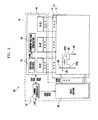
- FIG. 1 is a perspective view illustrating a mobile terminal according to an exemplary embodiment of the present invention.
- FIG. 1 is a perspective view illustrating a mobile terminal according to an exemplary embodiment of the present invention.
- the mobile terminal of FIG. 1 includes an LCD device 10 for displaying images, an abnormal signal detection circuit 110 for detecting signals causing a white or black effect, a system controller 120 for controlling signals provided including video signals to the LCD device 10, and a power source 130 supplying a voltage for operating the mobile terminal 1.
- the LCD device 10 converts analog video signals and control signals received from the system controller 120 into digital signals required to drive the display panel of the LCD device 10.
- the LCD device 10 includes an LCD panel 6 and an LDI 8 for driving the LCD panel 6.
- the LCD panel 6 is formed by abutting an upper substrate 2 and a lower substrate 4, liquid crystal filled out between the substrates 2 and 4, and a plurality of spacers arranged for uniformly maintaining a gap between the substrates.
- the upper substrate 2 of the LCD panel 6 is provided with a common electrode, a planarization layer, a color filter, and a black matrix.
- the lower substrate 4 of the LCD panel 6 includes gate lines 26 and data lines 24 crossing the gate lines 26 to define a liquid crystal cell 28, which is independently driven by a thin film transistor (TFT) 32.
- a gate terminal 31 a of the TFT 32 is coupled with a gate line 26 and a source terminal 31b of the TFT 32 is coupled with a data line 24.
- the TFT 32 facilitates the provision of a pixel signal to the liquid crystal cell 28 through the data line 24 in response to a scan signal from the gate line 26.
- the liquid crystal cell 28 expresses a gradient by adjusting light transmission by varying alignments of liquid crystal molecules which have a dielectric anisotropic property according to an electric field formed by a difference between the common voltage provided to the common electrode and the pixel voltage provided to the pixel electrode.
- the LDI 8 includes a timing controller 12, a data driver 14, a gate driver 16, a voltage source 18, and a common voltage generator 19.
- the timing controller 12 generates gate control signals (gate start pulse (GSP), gate shift clock (GSC), gate output enable (GOE) signals) for controlling operation of the gate driver 16 and data control signals (source start pulse (SSP), source shift clock (SSC), source output enable (SOE), polarity control (POL) signals) for controlling operation of the gate driver, using synchronization signals (H, V) provided from the system controller 120.
- the timing controller 12 also converts the data signals received from the system controller 120 to properly drive the LCD panel 6 and then transmits the converted signal to the data driver 14.
- the data driver 14 provides the pixel signals for every horizontal period by the data line 24.
- the data driver 14 provides the pixel signals to the data lines 24 in response to the data control signals (SSP, SSC, SOE, POL) provided from the timing controller 12.
- the data driver 14 also converts the pixel data from the timing controller 12 to analog pixel signals using a gamma voltage provided from a gamma voltage generator (not shown).
- the data driver 14 generates a sampling signal by shifting a source start pulse (SSP) according to a source shift clock (SSC). The data driver 14 then sequentially latches the pixel data in a predetermined unit in response to the sampling signal. According to an exemplary implementation, the data driver 14 converts the latched pixel data per line into an analog pixel signal and provides the analog pixel signal to the data lines 24 during a SOE duration. The data driver 14 converts the pixel data into a positive or negative pixel signal in response to a POL.
- the gate driver 16 drives the gate lines 26 in a sequential order under the control of the timing controller 12.
- the gate driver 16 provides gate high voltage to the gate lines 26 in a sequential order in response to the gate control signals (GSP, GSC, GOE).
- the gate driver 16 generates shift pulse by shifting the gate start pulse (GSP) according to a gate shift clock (GSC).
- GSC gate shift clock
- the gate driver 16 then provides the gate high voltage to the gate lines 26 every horizontal period in response to the shift pulse.
- the shift pulse is shifted one line after another every horizontal period and the gate driver 16 provides the gate high voltage to the gate line 26 corresponding to the shift pulse.
- the gate driver 16 provides the gate low voltage to the gate lines 26 when the gate high voltage is not provided.
- the voltage source 18 generates voltages required for operating the LCD device using the input voltage from the system power source 130 and provides the voltages to the timing controller 12, common voltage generator 19, data driver 14, and gate driver 16.
- the common voltage generator 19 generates a common voltage using a reference signal (VRS) from the voltage source 18.
- the common voltage is a reference voltage for driving the liquid crystal cell 28.
- the abnormal signal detection circuit 110 is structured to detect a value of the signal provided from a specific line of the LDI 8 of the LCD device 10. Referring to FIG. 3, the abnormal signal detection circuit 110 is implemented to detect a signal on the reference signal line providing the signal having the lowest voltage level among the voltage-related signals of the LDI 8, and to provide the detected signal to the system controller 120.
- the abnormal signal detection circuit 110 can use the gate high voltage or gate low voltage, which is generated by the gate driver 16 and provided to the LCD panel 6.
- the gate high voltage (VGH) has a voltage level of 13 ⁇ 15V and the gate low voltage (VGL) is about -10V such that the difference is less than 25V.
- the black effect typically occurs when the gate high voltage (VGH) is about 2.8V and the gate low voltage (VGL) is about 0V.
- the abnormal signal detection circuit 110 can be installed for sensing the gate low voltage (VGL) and gate high voltage (VGH) on the gate line 26 or can be implemented with an additional abnormal signal detection line, resulting in prediction of black or white effect occurrence.
- the system controller 120 controls the overall operation of the mobile terminal and especially provides signals for displaying images on the LCD device 10.
- the system controller 120 initializes the LCD device by controlling a power-on sequence of the voltage source 18 of the LCD device 10 by adjusting the system power source 130.
- the system controller 120 monitors the reference signal (VRS) provided to the LCD panel 6 from the voltage source 18 of the LCD device 10.
- the abnormal signal detection circuit 110 or the system controller 120 monitors a value of the reference signal (VRS) through the General Purpose Input/Output (GPIO) port. If the reference signal (VRS) fluctuates, the system controller 120 predicts occurrence of the black or white effect and controls the system power source 130. That is, the system controller 120 initializes the power sequence of the voltage source 18 of the LCD device 10 by controlling the system power source 130.
- the interoperation among the LCD device 10, the abnormal signal detection circuit 110, and the system controller 120 is described. However, exemplary embodiments of the present invention are not limited thereto, and can be implemented with an individual element constituting the mobile terminal.
- the system controller 120 can perform the function of the abnormal signal detection circuit 110.
- the abnormal signal detection circuit 110 is not required.
- the abnormal signal detection circuit 110 is implemented to cooperate with the LCD device 10, the system controller 120, a detection line and the system power source 130.
- the system controller 120 compares the signals generated by the LCD device 10 with the reference signals and initializes the LCD device 10 when the difference between the compared signals is greater than a tolerable value.
- the detection line connects the LCD device 10 and the system controller 120 and transfers the detected signal to the system controller 120.
- the system power source 130 supplies power to the LCD device 10.
- the voltage from the reference signal (VRS) is stepped down to a selected level for proper operation of the system controller 120, so that the abnormal signal detection circuit 110 acts as a system controller protection circuit.
- the initialization of the LCD device 10 is performed in a clam shell type mobile terminal, when the clam shell is closed and then opened and in a slide type mobile terminal, when a sliding member is slid up.
- the power sequence is depicted in FIG. 4 when the LCD device 10 is in a normal mode.
- the system controller 120 is provided with a code initializing the LCD power-on sequence for controlling the voltage source 18 of the LCD device 10 to control the voltage source 18 and the system power source 130.
- the system power source 130 supplies power required for operating the mobile terminal 1.
- FIG. 5 is a block diagram illustrating a configuration of the mobile terminal of FIG. 1 according to an exemplary embodiment of the present invention.
- the mobile terminal 1 includes the LCD device 10, the abnormal signal detection circuit 110 for detecting a signal causing the black or white effect, a system controller 120 providing data signals to the LCD device 10, the system power source 130 for supplying power required to operate the mobile terminal 1, a radio frequency (RF) unit 501, a data processing unit 503, an audio processing unit 505, and a keypad unit 507. Since the LCD device 10, the abnormal signal detection circuit 110, the system controller 120, and the system power source 130 have structures and functions identical to the mobile terminal of FIG. 1, detailed descriptions of these elements are omitted for clarity and conciseness.
- the RF unit 501 comprises a radio frequency transmitter and a radio frequency receiver, which are both coupled to an antenna which is used for transmitting and receiving radio signals through an air channel.
- the RF unit 501 is coupled to the data processing unit 503, which processes digital signals into a form that can be transmitted by the transmitter of RF unit 501 or processes baseband signals received and modulated by the receiver of the RF unit 501 into digital form for other units of the portable phone.
- the data processing unit 503 includes a means for encoding and modulating a signal to be transmitted through the RF unit 501 and a means for demodulating and decoding a signal received through the RF unit 501.
- the signals received through the data processing unit 503 are transferred to the LCD device 10 to be displayed as an image under the control of the system controller 120.
- the audio processing unit 505 converts analog audio signals received at a microphone (MIC) into digital signals and converts digital audio signals received from the data processing unit 503 into analog audio signals to be played over a speaker (SPK).
- the keypad unit 507 includes a plurality of alphanumeric keys for facilitating a user's ability to input alphanumeric characters and various function keys enabling the user to input commands for operating corresponding functions.
- the keypad unit 507 also includes a turn-on and turn-off key for turning on and turning off the mobile terminal 1.
- FIG. 6 is a schematic block diagram illustrating a white/ black effect control part of an LCD device according to an exemplary embodiment of the present invention.
- the mobile terminal includes an LCD device 10, a power source 130 and a system controller 120.
- the power source 130 supplies power to the LCD device 10 and the power source 130 controls the voltage source 18.
- the system controller 120 controls the general operation of the LCD device 10, determines an occurrence of a black or white effect when a variation of the reference signal (VRS) is detected from the LCD device 10, and adjusts the black or white effect by controlling the power source 130 to initialize the LCD device 10, such as initializing the voltage source 18 of the LCD device 10.
- the system controller 120 is provided with a GPIO port for detecting the reference signal (VRS).
- the GPIO port is connected to the voltage source 18 for supplying the reference signal (VRS).
- the system controller 120 compares a value of the reference signal (VRS) detected through the GPIO port with a value of the normal state reference signal (VRS) to verify a difference between the two values, and controls to initialize the LCD device according to the difference.
- the system controller 120 inspects the gate driver and gate lines of LDI of the LCD device 10 to verify the variation of the gate high voltage and gate low voltage supplied to the gate driver and the gate lines.
- the system controller 120 can detect abnormal gate voltage and control the power source 130 for handling the black or white effect of the LCD device 10.
- a detection circuit is removed, and a GPIO port is directly connected to the LCD device 10 for sensing the signal variation.
- the system controller 120 may perform a voltage or current drop when the signal input to the GPIO port has a high voltage or current value for stabilizing the GPIO port.
- FIG. 7 is a flowchart illustrating an LCD device driving method according to an exemplary embodiment of the present invention.
- the mobile terminal 10 initially detects a signal from the LDI 8(S101).
- the abnormal signal detection circuit 110 detects the signals generated by the voltage source 18 and the gate driver 16.
- the abnormal signal detection circuit 110 detects the reference signal (VRS) provided from the voltage source 18 to the common voltage generator 19 or detects the gate high voltage (VGH) and the gate low voltage (VGL) provided from the gate driver 16 to the LCD panel 6.
- VRS reference signal
- VGH gate high voltage
- VGL gate low voltage
- Separately added detection lines can be formed at the voltage source 18 generating the reference signal (VRS) or the gate driver 16 generating the gate high voltage (VGH) and the gate low voltage (VGL) in order to detect the signals.
- the detected signal is transfers to the system controller 120, and the system controller 120 compares the detected signal with a normal state signal and determines whether the detected signal corresponds to the normal state signal (S102). If the detected signal is, for example, substantially equal to the normal state signal, the mobile terminal repeats the step S101. If the detected signal is not equal to the normal state signal, the mobile terminal initializes the power-on sequence of the voltage source 18 (S103). At step S103, the system controller 120 transmits a control signal for initializing the power-on sequence of the voltage source 18 of the LCD device 10 to the voltage source 18 such that the voltage source 18 resets the power-on sequence according to the control signal, resulting in a non-occurrence of the black or white effect.
- the black or white effect of the LCD device is detected using an abnormal signal detection circuit 110.
- the exemplary embodiment of the present invention is not limited thereto but can be implemented such that the system controller 120 directly detects the signal generated at LDI of the LCD device 10.
- an LCD device of a mobile terminal and the driving method of the LCD device according to the exemplary embodiments of the present invention can predict an occurrence of a black or white effect and avoid the occurrence of the black or white effect by initializing the input voltage of the LCD device.
- the LCD device of a mobile terminal and the driving method of the LCD device according to an exemplary embodiment of the present invention are capable of enhancing display quality of an LCD panel of the LCD device by protecting the LCD panel from experiencing a white or black effect.
- the LCD device of a mobile terminal and the driving method of the LCD device according to exemplary embodiments of the present invention improve productivity by removing an insulation tape application process, which requires expensive insulation tape and equipment, time, and labor to adhere the insulation tape.
Landscapes
- Engineering & Computer Science (AREA)
- Chemical & Material Sciences (AREA)
- Crystallography & Structural Chemistry (AREA)
- Physics & Mathematics (AREA)
- Computer Hardware Design (AREA)
- General Physics & Mathematics (AREA)
- Theoretical Computer Science (AREA)
- Control Of Indicators Other Than Cathode Ray Tubes (AREA)
- Testing Electric Properties And Detecting Electric Faults (AREA)
- Liquid Crystal Display Device Control (AREA)
Applications Claiming Priority (2)
| Application Number | Priority Date | Filing Date | Title |
|---|---|---|---|
| KR20060064432 | 2006-07-10 | ||
| KR1020070005661A KR100843326B1 (ko) | 2006-07-10 | 2007-01-18 | 액정표시장치와 액정표시장치 구동방법 및 이를 포함하는휴대 단말기 |
Publications (2)
| Publication Number | Publication Date |
|---|---|
| EP1879166A2 true EP1879166A2 (de) | 2008-01-16 |
| EP1879166A3 EP1879166A3 (de) | 2009-08-19 |
Family
ID=38596203
Family Applications (1)
| Application Number | Title | Priority Date | Filing Date |
|---|---|---|---|
| EP07012146A Withdrawn EP1879166A3 (de) | 2006-07-10 | 2007-06-21 | Flüssigkristallanzeigevorrichtung und Ansteuerungsverfahren und mobiles Endgerät damit |
Country Status (2)
| Country | Link |
|---|---|
| US (1) | US8502812B2 (de) |
| EP (1) | EP1879166A3 (de) |
Families Citing this family (4)
| Publication number | Priority date | Publication date | Assignee | Title |
|---|---|---|---|---|
| KR102435257B1 (ko) * | 2015-08-04 | 2022-08-25 | 삼성디스플레이 주식회사 | 게이트 보호회로 및 이를 포함하는 표시장치 |
| KR102531460B1 (ko) | 2016-03-24 | 2023-05-12 | 삼성전자주식회사 | 디스플레이 구동 장치 및 이를 포함하는 디스플레이 장치 |
| JP2020140017A (ja) | 2019-02-27 | 2020-09-03 | 三菱電機株式会社 | 駆動回路、液晶駆動コントローラ、及び、液晶表示装置 |
| US11726934B2 (en) * | 2021-09-08 | 2023-08-15 | Level 3 Communications, Llc | Systems and methods for configuration of sequence handlers |
Family Cites Families (25)
| Publication number | Priority date | Publication date | Assignee | Title |
|---|---|---|---|---|
| JP2840374B2 (ja) | 1990-04-13 | 1998-12-24 | キヤノン株式会社 | 表示制御装置 |
| JP3312423B2 (ja) * | 1993-06-21 | 2002-08-05 | ソニー株式会社 | 平面表示装置、アクティブマトリクス基板および検査方法 |
| US5625373A (en) * | 1994-07-14 | 1997-04-29 | Honeywell Inc. | Flat panel convergence circuit |
| JP3108616B2 (ja) * | 1995-11-01 | 2000-11-13 | シャープ株式会社 | 液晶表示装置及び液晶表示装置を備えた無線受信装置 |
| JPH11296134A (ja) | 1998-04-10 | 1999-10-29 | Sony Corp | 表示装置の表示制御方法及び表示制御装置 |
| KR100490391B1 (ko) | 1998-06-11 | 2005-08-01 | 삼성전자주식회사 | 엘.씨.디를 구비한 컴퓨터의 비디오 모드 제어장치 및 그 방법 |
| TW407256B (en) * | 1998-10-16 | 2000-10-01 | Samsung Electronics Co Ltd | Power supply apparatus of an LCD and voltage sequence control method |
| KR100536833B1 (ko) * | 1999-07-05 | 2005-12-14 | 엘지.필립스 엘시디 주식회사 | 액정표시소자의 화이트스크린 에러 방지방법 및 그에 따른 장치 |
| KR100311476B1 (ko) * | 1999-08-16 | 2001-10-18 | 구자홍 | 평판형 영상표시기기의 화면보호 장치 및 방법 |
| US6615360B1 (en) * | 2000-01-25 | 2003-09-02 | International Business Machines Corporation | Method and system for controlling a power on sequence in response to monitoring respective components of a computer system with multiple CPU sockets to determine proper functionality |
| KR100358694B1 (ko) * | 2000-11-23 | 2002-10-30 | 삼성전자 주식회사 | 디스플레이 장치, 이상 동작 방지 회로 및 방법 |
| KR100400270B1 (ko) * | 2001-10-15 | 2003-10-01 | 엘지전자 주식회사 | 이동통신단말기에서 액정표시화면의 록크 업 방지장치 및그 방법 |
| US7698573B2 (en) * | 2002-04-02 | 2010-04-13 | Sharp Corporation | Power source apparatus for display and image display apparatus |
| KR100425765B1 (ko) * | 2002-04-12 | 2004-04-01 | 엘지.필립스 엘시디 주식회사 | 액정표시장치 |
| KR100927013B1 (ko) * | 2002-11-22 | 2009-11-16 | 엘지디스플레이 주식회사 | 액정표시장치 및 그 구동방법 |
| KR100891122B1 (ko) * | 2002-12-23 | 2009-04-06 | 엘지디스플레이 주식회사 | 전압유기 방지회로를 구비한 타이밍컨트롤러 리셋회로 |
| KR100531850B1 (ko) | 2003-02-15 | 2005-11-30 | 엘지전자 주식회사 | 휴대 단말기의 표시부 리셋 장치 및 방법 |
| KR100598063B1 (ko) | 2004-06-25 | 2006-07-10 | 주식회사 팬택앤큐리텔 | 백화현상 방지 장치 및 그 방법 |
| JP2006017891A (ja) * | 2004-06-30 | 2006-01-19 | Canon Inc | 表示装置およびテレビジョン装置 |
| US20060158421A1 (en) * | 2004-12-20 | 2006-07-20 | Kabushiki Kaisha Toshiba | Driver circuit of display device and method of driving the same |
| KR101133763B1 (ko) * | 2005-02-02 | 2012-04-09 | 삼성전자주식회사 | 액정 표시 장치의 구동 장치 및 이를 포함하는 액정 표시장치 |
| KR20060090076A (ko) * | 2005-02-07 | 2006-08-10 | 삼성전자주식회사 | 표시 장치와 이의 구동 방법 |
| JP4172471B2 (ja) * | 2005-06-17 | 2008-10-29 | セイコーエプソン株式会社 | 駆動回路、電気光学装置及び電子機器 |
| KR101157949B1 (ko) * | 2005-06-29 | 2012-06-25 | 엘지디스플레이 주식회사 | 보호회로, 이의 구동방법, 이를 사용한 액정표시장치, 및이를 사용한 액정표시장치의 구동방법 |
| KR100781681B1 (ko) | 2005-09-06 | 2007-12-04 | 엘지전자 주식회사 | Lcd 백화 현상 검출 방법 및 장치 |
-
2007
- 2007-05-16 US US11/798,697 patent/US8502812B2/en not_active Expired - Fee Related
- 2007-06-21 EP EP07012146A patent/EP1879166A3/de not_active Withdrawn
Non-Patent Citations (1)
| Title |
|---|
| None |
Also Published As
| Publication number | Publication date |
|---|---|
| US20080043011A1 (en) | 2008-02-21 |
| EP1879166A3 (de) | 2009-08-19 |
| US8502812B2 (en) | 2013-08-06 |
Similar Documents
| Publication | Publication Date | Title |
|---|---|---|
| US8593491B2 (en) | Application of voltage to data lines during Vcom toggling | |
| US9153186B2 (en) | Devices and methods for kickback-offset display turn-off | |
| US8866697B2 (en) | Display device and mobile device including display device | |
| US8164563B2 (en) | Data multiplexer architecture for realizing dot inversion mode for use in a liquid crystal display device and associated driving method | |
| US9953561B2 (en) | Array substrate of display apparatus and driving method thereof and display apparatus | |
| TWI512381B (zh) | 用於放電具有氧化物薄膜電晶體之像素之裝置與方法 | |
| US9201540B2 (en) | Charge recycling system and method | |
| WO2013185053A1 (en) | Devices and methods for improving image quality in a display having multiple vcoms | |
| US20170262119A1 (en) | Touch control device drive method, touch control device drive circuit and touch control device | |
| US8502812B2 (en) | Liquid crystal display device and driving method thereof, and mobile terminal having the same, for preventing white or black effect | |
| US8730229B2 (en) | Devices and methods for zero-bias display turn-off using VCOM switch | |
| US20030122756A1 (en) | Apparatus and method for driving image display device | |
| US9111500B2 (en) | Devices and methods for pixel discharge before display turn-off | |
| US7358944B2 (en) | Method and system for reducing residual image effect of liquid crystal display after turned off | |
| WO2021045388A1 (ko) | 디스플레이 장치 및 그 제어 방법 | |
| CN101105917B (zh) | 液晶显示器装置及其驱动方法和具有该装置的移动终端 | |
| WO2006038253A1 (ja) | 液晶表示装置 | |
| JP2004205588A (ja) | 表示装置及びその駆動制御方法 | |
| JP4905635B2 (ja) | 表示駆動装置 | |
| US11922897B2 (en) | Data driving circuit, display module, and display device | |
| KR100805541B1 (ko) | 전기 광학 장치, 전기 광학 장치의 구동 방법 및 전자기기 | |
| US7385578B2 (en) | Method for warming-up an LCD (liquid crystal display) system | |
| CN100476945C (zh) | 电光装置、其驱动方法及电子设备 | |
| KR101438219B1 (ko) | 액정표시장치의 플리커 방지장치 및 방법 | |
| CN108766328A (zh) | 检测电路及检测方法 |
Legal Events
| Date | Code | Title | Description |
|---|---|---|---|
| PUAI | Public reference made under article 153(3) epc to a published international application that has entered the european phase |
Free format text: ORIGINAL CODE: 0009012 |
|
| 17P | Request for examination filed |
Effective date: 20070621 |
|
| AK | Designated contracting states |
Kind code of ref document: A2 Designated state(s): AT BE BG CH CY CZ DE DK EE ES FI FR GB GR HU IE IS IT LI LT LU LV MC MT NL PL PT RO SE SI SK TR |
|
| AX | Request for extension of the european patent |
Extension state: AL BA HR MK YU |
|
| PUAL | Search report despatched |
Free format text: ORIGINAL CODE: 0009013 |
|
| AK | Designated contracting states |
Kind code of ref document: A3 Designated state(s): AT BE BG CH CY CZ DE DK EE ES FI FR GB GR HU IE IS IT LI LT LU LV MC MT NL PL PT RO SE SI SK TR |
|
| AX | Request for extension of the european patent |
Extension state: AL BA HR MK RS |
|
| 17Q | First examination report despatched |
Effective date: 20100226 |
|
| AKX | Designation fees paid |
Designated state(s): DE FR GB |
|
| RAP1 | Party data changed (applicant data changed or rights of an application transferred) |
Owner name: SAMSUNG ELECTRONICS CO., LTD. |
|
| STAA | Information on the status of an ep patent application or granted ep patent |
Free format text: STATUS: EXAMINATION IS IN PROGRESS |
|
| STAA | Information on the status of an ep patent application or granted ep patent |
Free format text: STATUS: THE APPLICATION IS DEEMED TO BE WITHDRAWN |
|
| 18D | Application deemed to be withdrawn |
Effective date: 20170103 |