EP1875505B1 - Oled multicolor displays - Google Patents
Oled multicolor displays Download PDFInfo
- Publication number
- EP1875505B1 EP1875505B1 EP06758429A EP06758429A EP1875505B1 EP 1875505 B1 EP1875505 B1 EP 1875505B1 EP 06758429 A EP06758429 A EP 06758429A EP 06758429 A EP06758429 A EP 06758429A EP 1875505 B1 EP1875505 B1 EP 1875505B1
- Authority
- EP
- European Patent Office
- Prior art keywords
- light
- light emitting
- pixel
- pixels
- emitting layer
- Prior art date
- Legal status (The legal status is an assumption and is not a legal conclusion. Google has not performed a legal analysis and makes no representation as to the accuracy of the status listed.)
- Active
Links
Images


Classifications
-
- C—CHEMISTRY; METALLURGY
- C09—DYES; PAINTS; POLISHES; NATURAL RESINS; ADHESIVES; COMPOSITIONS NOT OTHERWISE PROVIDED FOR; APPLICATIONS OF MATERIALS NOT OTHERWISE PROVIDED FOR
- C09K—MATERIALS FOR MISCELLANEOUS APPLICATIONS, NOT PROVIDED FOR ELSEWHERE
- C09K11/00—Luminescent, e.g. electroluminescent, chemiluminescent materials
- C09K11/06—Luminescent, e.g. electroluminescent, chemiluminescent materials containing organic luminescent materials
-
- H—ELECTRICITY
- H05—ELECTRIC TECHNIQUES NOT OTHERWISE PROVIDED FOR
- H05B—ELECTRIC HEATING; ELECTRIC LIGHT SOURCES NOT OTHERWISE PROVIDED FOR; CIRCUIT ARRANGEMENTS FOR ELECTRIC LIGHT SOURCES, IN GENERAL
- H05B33/00—Electroluminescent light sources
- H05B33/12—Light sources with substantially two-dimensional radiating surfaces
- H05B33/14—Light sources with substantially two-dimensional radiating surfaces characterised by the chemical or physical composition or the arrangement of the electroluminescent material, or by the simultaneous addition of the electroluminescent material in or onto the light source
-
- H—ELECTRICITY
- H10—SEMICONDUCTOR DEVICES; ELECTRIC SOLID-STATE DEVICES NOT OTHERWISE PROVIDED FOR
- H10K—ORGANIC ELECTRIC SOLID-STATE DEVICES
- H10K59/00—Integrated devices, or assemblies of multiple devices, comprising at least one organic light-emitting element covered by group H10K50/00
- H10K59/30—Devices specially adapted for multicolour light emission
- H10K59/38—Devices specially adapted for multicolour light emission comprising colour filters or colour changing media [CCM]
-
- C—CHEMISTRY; METALLURGY
- C09—DYES; PAINTS; POLISHES; NATURAL RESINS; ADHESIVES; COMPOSITIONS NOT OTHERWISE PROVIDED FOR; APPLICATIONS OF MATERIALS NOT OTHERWISE PROVIDED FOR
- C09K—MATERIALS FOR MISCELLANEOUS APPLICATIONS, NOT PROVIDED FOR ELSEWHERE
- C09K2211/00—Chemical nature of organic luminescent or tenebrescent compounds
- C09K2211/10—Non-macromolecular compounds
- C09K2211/1003—Carbocyclic compounds
- C09K2211/1007—Non-condensed systems
-
- C—CHEMISTRY; METALLURGY
- C09—DYES; PAINTS; POLISHES; NATURAL RESINS; ADHESIVES; COMPOSITIONS NOT OTHERWISE PROVIDED FOR; APPLICATIONS OF MATERIALS NOT OTHERWISE PROVIDED FOR
- C09K—MATERIALS FOR MISCELLANEOUS APPLICATIONS, NOT PROVIDED FOR ELSEWHERE
- C09K2211/00—Chemical nature of organic luminescent or tenebrescent compounds
- C09K2211/10—Non-macromolecular compounds
- C09K2211/1003—Carbocyclic compounds
- C09K2211/1011—Condensed systems
-
- C—CHEMISTRY; METALLURGY
- C09—DYES; PAINTS; POLISHES; NATURAL RESINS; ADHESIVES; COMPOSITIONS NOT OTHERWISE PROVIDED FOR; APPLICATIONS OF MATERIALS NOT OTHERWISE PROVIDED FOR
- C09K—MATERIALS FOR MISCELLANEOUS APPLICATIONS, NOT PROVIDED FOR ELSEWHERE
- C09K2211/00—Chemical nature of organic luminescent or tenebrescent compounds
- C09K2211/10—Non-macromolecular compounds
- C09K2211/1003—Carbocyclic compounds
- C09K2211/1014—Carbocyclic compounds bridged by heteroatoms, e.g. N, P, Si or B
-
- C—CHEMISTRY; METALLURGY
- C09—DYES; PAINTS; POLISHES; NATURAL RESINS; ADHESIVES; COMPOSITIONS NOT OTHERWISE PROVIDED FOR; APPLICATIONS OF MATERIALS NOT OTHERWISE PROVIDED FOR
- C09K—MATERIALS FOR MISCELLANEOUS APPLICATIONS, NOT PROVIDED FOR ELSEWHERE
- C09K2211/00—Chemical nature of organic luminescent or tenebrescent compounds
- C09K2211/10—Non-macromolecular compounds
- C09K2211/1018—Heterocyclic compounds
- C09K2211/1025—Heterocyclic compounds characterised by ligands
- C09K2211/1029—Heterocyclic compounds characterised by ligands containing one nitrogen atom as the heteroatom
- C09K2211/1033—Heterocyclic compounds characterised by ligands containing one nitrogen atom as the heteroatom with oxygen
-
- C—CHEMISTRY; METALLURGY
- C09—DYES; PAINTS; POLISHES; NATURAL RESINS; ADHESIVES; COMPOSITIONS NOT OTHERWISE PROVIDED FOR; APPLICATIONS OF MATERIALS NOT OTHERWISE PROVIDED FOR
- C09K—MATERIALS FOR MISCELLANEOUS APPLICATIONS, NOT PROVIDED FOR ELSEWHERE
- C09K2211/00—Chemical nature of organic luminescent or tenebrescent compounds
- C09K2211/10—Non-macromolecular compounds
- C09K2211/1018—Heterocyclic compounds
- C09K2211/1025—Heterocyclic compounds characterised by ligands
- C09K2211/1029—Heterocyclic compounds characterised by ligands containing one nitrogen atom as the heteroatom
- C09K2211/1037—Heterocyclic compounds characterised by ligands containing one nitrogen atom as the heteroatom with sulfur
-
- C—CHEMISTRY; METALLURGY
- C09—DYES; PAINTS; POLISHES; NATURAL RESINS; ADHESIVES; COMPOSITIONS NOT OTHERWISE PROVIDED FOR; APPLICATIONS OF MATERIALS NOT OTHERWISE PROVIDED FOR
- C09K—MATERIALS FOR MISCELLANEOUS APPLICATIONS, NOT PROVIDED FOR ELSEWHERE
- C09K2211/00—Chemical nature of organic luminescent or tenebrescent compounds
- C09K2211/10—Non-macromolecular compounds
- C09K2211/1018—Heterocyclic compounds
- C09K2211/1025—Heterocyclic compounds characterised by ligands
- C09K2211/1044—Heterocyclic compounds characterised by ligands containing two nitrogen atoms as heteroatoms
-
- C—CHEMISTRY; METALLURGY
- C09—DYES; PAINTS; POLISHES; NATURAL RESINS; ADHESIVES; COMPOSITIONS NOT OTHERWISE PROVIDED FOR; APPLICATIONS OF MATERIALS NOT OTHERWISE PROVIDED FOR
- C09K—MATERIALS FOR MISCELLANEOUS APPLICATIONS, NOT PROVIDED FOR ELSEWHERE
- C09K2211/00—Chemical nature of organic luminescent or tenebrescent compounds
- C09K2211/10—Non-macromolecular compounds
- C09K2211/1018—Heterocyclic compounds
- C09K2211/1025—Heterocyclic compounds characterised by ligands
- C09K2211/1059—Heterocyclic compounds characterised by ligands containing three nitrogen atoms as heteroatoms
- C09K2211/107—Heterocyclic compounds characterised by ligands containing three nitrogen atoms as heteroatoms with other heteroatoms
-
- C—CHEMISTRY; METALLURGY
- C09—DYES; PAINTS; POLISHES; NATURAL RESINS; ADHESIVES; COMPOSITIONS NOT OTHERWISE PROVIDED FOR; APPLICATIONS OF MATERIALS NOT OTHERWISE PROVIDED FOR
- C09K—MATERIALS FOR MISCELLANEOUS APPLICATIONS, NOT PROVIDED FOR ELSEWHERE
- C09K2211/00—Chemical nature of organic luminescent or tenebrescent compounds
- C09K2211/10—Non-macromolecular compounds
- C09K2211/1018—Heterocyclic compounds
- C09K2211/1025—Heterocyclic compounds characterised by ligands
- C09K2211/1088—Heterocyclic compounds characterised by ligands containing oxygen as the only heteroatom
-
- H—ELECTRICITY
- H10—SEMICONDUCTOR DEVICES; ELECTRIC SOLID-STATE DEVICES NOT OTHERWISE PROVIDED FOR
- H10K—ORGANIC ELECTRIC SOLID-STATE DEVICES
- H10K50/00—Organic light-emitting devices
- H10K50/10—OLEDs or polymer light-emitting diodes [PLED]
- H10K50/11—OLEDs or polymer light-emitting diodes [PLED] characterised by the electroluminescent [EL] layers
- H10K50/125—OLEDs or polymer light-emitting diodes [PLED] characterised by the electroluminescent [EL] layers specially adapted for multicolour light emission, e.g. for emitting white light
-
- H—ELECTRICITY
- H10—SEMICONDUCTOR DEVICES; ELECTRIC SOLID-STATE DEVICES NOT OTHERWISE PROVIDED FOR
- H10K—ORGANIC ELECTRIC SOLID-STATE DEVICES
- H10K59/00—Integrated devices, or assemblies of multiple devices, comprising at least one organic light-emitting element covered by group H10K50/00
- H10K59/30—Devices specially adapted for multicolour light emission
- H10K59/35—Devices specially adapted for multicolour light emission comprising red-green-blue [RGB] subpixels
- H10K59/351—Devices specially adapted for multicolour light emission comprising red-green-blue [RGB] subpixels comprising more than three subpixels, e.g. red-green-blue-white [RGBW]
-
- H—ELECTRICITY
- H10—SEMICONDUCTOR DEVICES; ELECTRIC SOLID-STATE DEVICES NOT OTHERWISE PROVIDED FOR
- H10K—ORGANIC ELECTRIC SOLID-STATE DEVICES
- H10K71/00—Manufacture or treatment specially adapted for the organic devices covered by this subclass
- H10K71/60—Forming conductive regions or layers, e.g. electrodes
-
- H—ELECTRICITY
- H10—SEMICONDUCTOR DEVICES; ELECTRIC SOLID-STATE DEVICES NOT OTHERWISE PROVIDED FOR
- H10K—ORGANIC ELECTRIC SOLID-STATE DEVICES
- H10K85/00—Organic materials used in the body or electrodes of devices covered by this subclass
- H10K85/30—Coordination compounds
- H10K85/321—Metal complexes comprising a group IIIA element, e.g. Tris (8-hydroxyquinoline) gallium [Gaq3]
- H10K85/324—Metal complexes comprising a group IIIA element, e.g. Tris (8-hydroxyquinoline) gallium [Gaq3] comprising aluminium, e.g. Alq3
-
- H—ELECTRICITY
- H10—SEMICONDUCTOR DEVICES; ELECTRIC SOLID-STATE DEVICES NOT OTHERWISE PROVIDED FOR
- H10K—ORGANIC ELECTRIC SOLID-STATE DEVICES
- H10K85/00—Organic materials used in the body or electrodes of devices covered by this subclass
- H10K85/40—Organosilicon compounds, e.g. TIPS pentacene
-
- H—ELECTRICITY
- H10—SEMICONDUCTOR DEVICES; ELECTRIC SOLID-STATE DEVICES NOT OTHERWISE PROVIDED FOR
- H10K—ORGANIC ELECTRIC SOLID-STATE DEVICES
- H10K85/00—Organic materials used in the body or electrodes of devices covered by this subclass
- H10K85/60—Organic compounds having low molecular weight
- H10K85/611—Charge transfer complexes
-
- H—ELECTRICITY
- H10—SEMICONDUCTOR DEVICES; ELECTRIC SOLID-STATE DEVICES NOT OTHERWISE PROVIDED FOR
- H10K—ORGANIC ELECTRIC SOLID-STATE DEVICES
- H10K85/00—Organic materials used in the body or electrodes of devices covered by this subclass
- H10K85/60—Organic compounds having low molecular weight
- H10K85/615—Polycyclic condensed aromatic hydrocarbons, e.g. anthracene
-
- H—ELECTRICITY
- H10—SEMICONDUCTOR DEVICES; ELECTRIC SOLID-STATE DEVICES NOT OTHERWISE PROVIDED FOR
- H10K—ORGANIC ELECTRIC SOLID-STATE DEVICES
- H10K85/00—Organic materials used in the body or electrodes of devices covered by this subclass
- H10K85/60—Organic compounds having low molecular weight
- H10K85/631—Amine compounds having at least two aryl rest on at least one amine-nitrogen atom, e.g. triphenylamine
-
- H—ELECTRICITY
- H10—SEMICONDUCTOR DEVICES; ELECTRIC SOLID-STATE DEVICES NOT OTHERWISE PROVIDED FOR
- H10K—ORGANIC ELECTRIC SOLID-STATE DEVICES
- H10K85/00—Organic materials used in the body or electrodes of devices covered by this subclass
- H10K85/60—Organic compounds having low molecular weight
- H10K85/649—Aromatic compounds comprising a hetero atom
Definitions
- OLED organic light emitting diodes
- an OLED is comprised of an anode for hole injection, a cathode for electron injection, and an organic media sandwiched between these electrodes to support charge recombination that yields emission of light.
- a plurality of individually addressable OLED elements are arranged in a matrix of pixels. Each pixel includes an independently addressable OLED and is capable of producing light.
- Such matrixes can be of the passive type where electroluminescent OLED layers are sandwiched between two sets of orthogonal electrodes (rows and columns).
- An example of a passive matrix driven OLED display device is described in U.S. Patent 5,276,380 .
- the OLED display can be constructed of the active matrix type where one or more circuit elements, such as a transistor or capacitor, is used to drive each OLED.
- one or more circuit elements such as a transistor or capacitor
- An example of an active matrix driven OLED display device is described in U.S. Patent 5,550,066 .
- US 2001/0043043 A1 discloses an organic electroluminescent display panel including a substrate, an organic light emitting layer between two electrodes, one of which is transparent, and a color filter layer formed by evaporating a pigment and/or an organic dye, the organic display panel being divided into a plurality of organic electroluminescent devices capable of being independently controlled.
- a multicolor display In order to construct a multicolor display, the pixels are arranged to produce a variety of colors.
- a multicolor display can be constructed to have red, green, and blue pixels.
- Such a display is referred to as an RGB display. Additional colors can be achieved by such a display by mixing the light emitted by the red, green, and blue subpixels in various ratios.
- OLED electroluminescent layers for each of the pixels. This results in the need to pattern one or more of the OLED electroluminescent layers such that it is precisely aligned with the desired pixel.
- OLED layers can be deposited through a shadow mask in order to selectively deposit only in the desired areas. Shadow masks should then be aligned with the target pixel. Such alignment processes, however, are more complicated and can slow manufacturing throughput.
- Shadow masks also tend to cause damage to the OLED pixels when the mask contacts the display substrate.
- Alternate methods of separately patterning OLED layers for each layer are also known. For example, a method of pattering the OLED layers by transferring the OLED material from a donor sheet by use of a laser is known. However, this method requires the use of consumable donor substrates and complex laser writing equipment. The process of writing each pixel with a laser can also reduce manufacturing throughput.
- Another example process for patterning OLED layers involves deposition of the OLED materials dissolved in a solvent as droplets by way of an ink jet print head. This method requires the precision placement of the ink jet droplets. As such, complex structures for controlling droplet placement and spread can be required and tolerances for the pixel area can be large.
- the present invention provides a multicolor OLED display having at least three different color pixels that can be made more effectively.
- a feature of the present invention is that multicolor OLED displays made in accordance with the present invention can provide improved power efficiency.
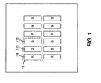
- FIG. 1 shows an example of a multicolor OLED display including three pixels that produce different colored light emission.
- pixel 11a preferably produces red light
- pixel 11b preferably produces green light
- pixel 11c preferably produces blue light.
- These pixels can be arranged in groups, such as pixel group 10. Although it is shown that each pixel group includes each of the differently colored pixels, the present invention is not limited to this case. Instead, some colored pixels can be present in greater number than other colored pixels.
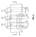
- FIG. 2 shows a top side view of pixels 11a , 11b , and 11c according to the first embodiment of the present invention.
- these pixels can be addressed by providing a matrix of orthogonal electrodes such as first electrodes 110a, 110b, and 110c and second electrode 130. That is, pixel 11a is constructed from first electrode 110a and second electrode 130, pixel 11b is constructed from first electrode 110b and second electrode 130 , and pixel 11c is constructed from first electrode 110c and second electrode 130.
- all pixels in a column share the same first electrode and all pixels in a row share the same second electrode.
- these pixels are arranged into a stripe pattern.
- the present invention is not limited to this arrangement and other arrangements such as delta pattern arrangements and quad arrangements can be applied by one skilled in the art.
- the present invention is not limited to the passive matrix configuration and an active matrix driving scheme can be applied by one skilled in the art.
- light emitting layer 123a is provided for pixels 11a and 11b so as to be common between both of these pixels. This requires light emitting layer 123a to be precisely aligned or patterned to these pixels.
- Light emitting layer 123c is provided for pixels 11a , 11b , and 11c and is common to all pixels, thus requiring no patterning step. In this manner, the number of precision aligned depositions required to form these three differently colored pixels is reduced from three to one.
- Light emitting layer 123a can be formed from a single step, such as for example, deposition through a single shadow mask, precise placement of one or more droplets from the same ink jet head, or transfer from the same donor sheet.
- Light emitting layer 123a is preferably arranged to emit light having a spectrum corresponding to a color between red and green, otherwise referred to as yellow-orange.
- Light emitting layer 123a is arranged so as to produce light having spectral components corresponding to the desired colors of both pixel 11a and pixel 11b . This can be achieved by forming a light emitting layer of materials that emit a wide spectrum of light in the red, red-orange, orange, yellow-orange, yellow, yellow-green, and green wavelengths.
- light emitting layer 123c is preferably arranged to emit light having a spectrum corresponding to a blue color.
- Light emitting layer 123c is arranged so as to produce light having spectral components corresponding to the desired color of pixel 11c .
- color filter 140a is formed in the path of the light emission, or in operative relationship, in pixel 11a to absorb undesired spectral components for pixel 11a and pass the desired spectral components corresponding to the desired red color.
- Color filter 140a can be constructed, for example, to transmit red light and absorb light having lower wavelengths.
- light emitting layer 123c is preferably arranged to emit light having a spectrum corresponding to a red color.
- Light emitting layer 123c is arranged so as to produce light having spectral components corresponding to the desired color of pixel 11c .
- light emitting layers 123a and 123c are overlapped for pixels 11a and 11b , the combination of light emitting layers 123a and 123c is arranged so as to produce light having mostly spectral components corresponding to the desired colors of both pixels 11a and 11b .
- color filter 140a is formed in the path of the light emission, or in operative relationship, in pixel 11a to absorb undesired spectral components for pixel 11a and pass the desired spectral components corresponding to the desired blue color.
- Color filter 140a can be constructed, for example, to transmit blue light and absorb light having higher wavelengths.
- color filter 140b is formed in the path of the light emission, or in operative relationship, in pixel 11b to absorb undesired spectral components for pixel 11b and pass the desired spectral components corresponding to the desired green color.
- Color filter 140b can be constructed, for example, to transmit green light and absorb light having different wavelengths.
- the red color desired for pixel 11c can be achieved with or without the use of a color filter.
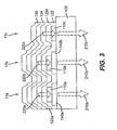
- FIG. 3 shows a cross sectional view of the device of FIG. 2 taken along line 3-3'.
- FIG. 3 shows that pixels 11a , 11b , and 11c produce internal light emission 220a, 220b, and 220c, respectively.
- Internal light emission 220c exits the device without filtration to become external light emission 210c .
- Internal light emission 220a passes through color filter 140a prior to exiting the device resulting in external light emission 210a.
- internal light emission 220b passes through color filter 140b prior to exiting the device resulting in external light emission 210b.
- Color filters 140a and 140b are preferably organic layers deposited by lamination or spin coating methods known in the art.
- the color filters are preferably photo-patternable as is known in the art wherein the color filter materials are deposited over the entire display surface, exposed with a light source, and either the exposed or the unexposed regions are removed by use of a solvent. This method provides effective alignment accuracy to the desired pixel region.
- the present invention is not limited to this preferred case, and other ways of depositing and patterning the color filter material as are known in the art can be employed by one skilled in the art.
- additional black matrix structures (not shown) which absorb some portion of all visible light can optionally be disposed in the non-emitting regions between pixels to reduce ambient light reflection and improve display contrast as is known in the art.
- color filter 140a is formed in the path of the light emission, or in operative relationship, in pixel 11a to absorb undesired spectral components for pixel 11a and pass the desired spectral components corresponding to the desired red color.
- color filter 140b is formed in the path of the light emission, or in operative relationship, in pixel 11b to absorb undesired spectral components for pixel 11b and pass the desired spectral components corresponding to the desired a green color.
- the blue color desired for pixel 11c can be achieved with or without the use of a color filter.
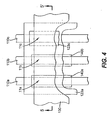
- Another alternate three pixel embodiment can be achieved by providing a first pixel emitting blue light, a second pixel emitting green light, and a third pixel emitting red light.
- the first light emitting layer 123a is preferably arranged to emit light having a spectrum corresponding to a color between blue and green, and produces light having spectral components corresponding to the desired colors of both pixel 11a and pixel 11b .
- light emitting layer 123c is preferably arranged to emit light having a spectrum corresponding to a red color, and produces light having spectral components corresponding to the desired color of pixel 11c .
- color filter 140a is formed in the path of the light emission, or in operative relationship, in pixel 11a to absorb undesired spectral components for pixel 11a and pass the desired spectral components corresponding to the desired blue color.
- Color filter 140a can be constructed, for example, to transmit blue light and absorb light having higher wavelengths.
- color filter 140b can be constructed, for example, to transmit green light and absorb light having different wavelengths.
- the red color desired for pixel 11c can be achieved with or without the use of a color filter.
- FIG. 5 shows a cross sectional view of the device of FIG. 4 taken along line 5-5'.
- FIG. 5 shows that pixels 11a , 11b , and 11c produce internal light emission 220a, 220b, and 220c, respectively.
- Internal light emission 220c exits the device without filtration to become external light emission 210c.
- Internal light emission 220a passes through color filter 140a prior to exiting the device resulting in external light emission 210a.
- internal light emission 220b passes through color filter 140b prior to exiting the device resulting in external light emission 210b.
- Color filters 140a and 140b are preferably organic layers as described previously.
- First electrodes 110a, 110b, and 110c are arranged to transmit light and are preferably constructed of a conductive transparent material such as indium tin oxide (ITO) or indium zinc oxide (IZO).
- Second electrode 130 is preferably constructed of a reflective conductive material such as previously described in order to achieve the desired light absorption or reflection properties and conductivity properties.
- Light emitting layer 123a is provided for pixels 11a , 11b and 11c so as to be common between these pixels, and therefore requires a precise alignment or patterning step.
- Light emitting layer 123c is provided for all pixels, and therefore does not require a precise alignment or patterning step. In this manner, the number of precision aligned depositions required to form these four differently colored pixels is reduced from four to one.
- Light emitting layers 123a and 123c can be formed as previously described.
- Light emitting layer 123a is preferably arranged to emit light having a spectrum corresponding to a color between red and green, and produces light having spectral components corresponding to the desired colors of pixels 11a, 11b , and 11c .
- light emitting layer 123c is preferably arranged to emit light having a spectrum corresponding to a blue color, and produces light having spectral components corresponding to the desired color of pixel 11c .
- light emitting layers 123a and 123c are overlapped for pixels 11a , 11b , and 11c
- the combination of light emitting layers 123a and 123c is arranged so as to produce light having mostly spectral components corresponding to the desired color of pixels 11a , 11b, and 11c .
- color filter 140a is formed in the path of the light emission in pixel 11a to absorb undesired spectral components and pass the desired spectral components corresponding to the desired red color.
- color filter 140c is formed in the path of the light emission in pixel 11c to absorb undesired spectral components and pass the desired spectral components corresponding to the desired green color.
- the desired color between red and green for pixel 11b is achieved without the use of a color filter.
- the blue color desired for pixel 11c can be achieved with or without the use of a color filter.
- a multicolor OLED display made in this manner can have higher power efficiency.
- the high efficiency unfiltered wide emission spectrum used in pixel 11b can be used frequently to replace either the lower efficiency red or green pixels to produce within gamut colors, as is known in the art.
- Efficiency can be measured for example in candelas (cd) per ampere (A) of current. As such high efficiency light emission results in displays that consume less power, or in other words, have high power efficiency.
- color filter 140a is formed in the path of the light emission in pixel 11a to absorb undesired spectral components and pass the desired spectral components corresponding to the desired blue color.
- color filter 140c is formed in the path of the light emission in pixel 11c to absorb undesired spectral components and pass the desired spectral components corresponding to the desired green color.
- the desired color between blue and green for pixel 11b is achieved without the use of a color filter.
- the red color desired for pixel 11d can be achieved with or without the use of a color filter.
- a multicolor OLED display made in this manner can have higher power efficiency.
- the high efficiency unfiltered wide emission spectrum used in pixel 11b can be used frequently to replace either the lower efficiency blue or green pixels to produce within gamut colors, as is known in the art.
- FIG. 8 shows a cross sectional view of the device of FIG. 7 taken along line 8-8'.
- FIG. 8 shows that pixels 11a, 11b , 11c , and 11d produce internal light emission 220a, 220b, 220c , and 220d, respectively.
- Internal light emission 220b and 220d exit the device without filtration to become external light emission 210b and 210d, respectively.
- Internal light emission 220a passes through color filter 140a prior to exiting the device resulting in external light emission 210a.
- internal light emission 220c passes through color filter 140c prior to exiting the device resulting in external light emission 210c.
- Color filters 140a and 140c are preferably organic layers as described previously.
- First electrodes 110a, 110b, 110c, and 110d are arranged to transmit light and are preferably constructed of a conductive transparent material such as previously described.
- Second electrode 130 is preferably constructed of a reflective conductive material such as previously described in order to achieve the desired light absorption or reflection properties and conductivity properties.
- Yet another alternate four pixel embodiment can be achieved by providing a fourth pixel to the second embodiment of this invention.
- the fourth pixel emits a color between that of the first and second pixels.
- a common first light emitting layer would be provided over the first, second, third, and fourth pixels, while the second light emitting layer would be provided only over the third pixel.
- the first and second pixels have color filters, while the third and fourth pixels have no color filters.
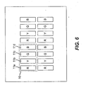
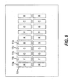
- FIG. 9 shows an embodiment of a multicolor OLED display including five pixels that produce different colored light emission.
- pixel 11a preferably produces red light
- pixel 11c preferably produces green light
- pixel 11e preferably produces blue light.
- Pixel 11b preferably produces light having a color between that of the red light of pixel 11a and the green light of pixel 11c .
- Pixel 11d preferably produces light having a color between that of the blue light of pixel 11e and the green light of pixel 11c .
- These pixels can be arranged in groups, such as pixel group 10. Although it is shown that each pixel group includes each of the differently colored pixels, the present invention is not limited to this case. Instead, some colored pixels can be present in greater number than other colored pixels. For example, there can be twice as many red pixels as there are yellow pixels. As such, each pixel group does not have to contain a pixel having every color.
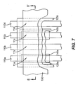
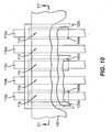
- FIG. 10 shows a top side view of pixels 11a , 11b , 11c , 11d , and 11e according to the fourth embodiment of the present invention.
- these pixels can be addressed by providing a matrix of orthogonal electrodes such as first electrodes 110a , 110b , 110c , 110d , and 110e and second electrode 130. That is pixel 11a is constructed from first electrode 110a and second electrode 130, pixel 11b is constructed from first electrode 110b and second electrode 130, pixel 11c is constructed from first electrode 110c and second electrode 130, pixel 11d is constructed from first electrode 110d and second electrode 130, and pixel 11e is constructed from first electrode 110e and second electrode 130.
- light emitting layer 123a is provided for pixels 11a , 11b , and 11c so as to be common between these pixels. This requires light emitting layer 123a to be precisely aligned or patterned to these pixels. Light emitting layer 123c is provided for all pixels, and therefore requires no precise alignment or patterning step. In this manner, the number of precision aligned depositions required to form these five differently colored pixels is reduced from five to one. Light emitting layers 123a and 123c can be formed as previously described. Light emitting layer 123a can be continuously formed between pixels 11a, 11b , and 11c as shown. This can be achieved, for example, by using a single opening in the shadow mask to deposit the entire layer.
- the pixels which share the same light emitting layer, are preferably disposed to be adjacent to one and other.
- pixel 11b is adjacent to pixel 11a and pixel 11c as shown.
- the present invention is not limited to this preferred embodiment and alternate embodiments where the light emitting layer is discontinuous between the two pixels or the two pixels are spaced apart are possible. Such alternate embodiments are still advantageous in that the number of precision aligned depositions is reduced.
- this unfiltered spectra emission is preferably used for pixel 11b .
- Light emitting layer 123c is preferably arranged to emit light having a spectrum corresponding to a color between red and green as described previously, and produces light having spectral components corresponding to the desired colors of pixels 11d and 11e . This can be achieved by forming a light emitting layer of materials that emit a wide spectrum of light in the red to green wavelengths. As such, this unfiltered spectra emission is preferably used for pixel 11d .
- color filter 140a is formed in the path of the light emission between the pixel and the viewer in pixel 11a to absorb undesired spectral components for pixel 11a and pass the desired spectral components corresponding to the desired blue color.
- color filter 140c is formed in the path of the light emission between the pixel and the viewer in pixel 11c to absorb undesired spectral components for pixel 11c and pass the desired spectral components corresponding to the desired green color.
- color filter 140e is formed in the path of the light emission between the pixel and the viewer in pixel 11e to absorb undesired spectral components for pixel 11e and pass the desired spectral components corresponding to the desired red color.
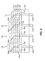
- FIG. 11 shows a cross sectional view of the device of FIG. 10 taken along line 11-11'.
- FIG. 11 shows that pixels 11a , 11b , 11c , 11d , and 11e produce internal light emission 220a, 220b, 220c, 220d, and 220e, respectively.
- Internal light emission 220b and 220d exit the device without filtration to become external light emission 210b and 210d .
- Internal light emission 220a passes through color filter 140a prior to exiting the device resulting in external light emission 210a.
- Internal light emission 220c passes through color filter 140c prior to exiting the device resulting in external light emission 210c .
- internal light emission 220e passes through color filter 140e prior to exiting the device resulting in external light emission 210e.
- Color filters 140a, 140c, and 140e are preferably organic layers as previously described.
- First electrodes 110a , 110b , 110c , 110d , and 110e are arranged to transmit light and are preferably constructed of a conductive transparent material such as previously described.
- Second electrode 130 is preferably constructed of a reflective conductive material such as previously described in order to achieve the desired light absorption or reflection properties and conductivity properties.
- a hole-injecting layer (not shown) be formed and disposed over first electrodes 110a , 110b , 110c , 110d , and 110e .
- the hole-injecting material can serve to improve the film formation property of subsequent organic layers and to facilitate injection of holes into the hole-transporting layer.
- Suitable materials for use in the hole-injecting layer include, but are not limited to, porphyrinic compounds as described in U.S. Patent 4,720,432 , plasma-deposited fluorocarbon polymers as described in U.S.
- Exemplary monomeric triarylamines are illustrated by Klupfel, et al. in U.S. Patent 3,180,730 .
- Other suitable triarylamines substituted with one or more vinyl radicals or at least one active hydrogen-containing group are disclosed by Brantley, et al. in U.S. Patents 3,567,450 and 3,658,520 .
- a more preferred class of aromatic tertiary amines is those that include at least two aromatic tertiary amine moieties as described in U.S. Patents 4,720,432 and 5,061,569 .
- Such compounds include those represented by structural Formula A wherein:
- At least one of Q 1 or Q 2 contains a polycyclic fused ring structure, e.g., a naphthalene moiety.
- G is an aryl group, it is conveniently a phenylene, biphenylene, or naphthalene moiety.
- a useful class of triarylamines satisfying structural Formula A and containing two triarylamine moieties is represented by structural Formula B where:
- tetraaryldiamines Another class of aromatic tertiary amines is the tetraaryldiamines. Desirable tetraaryldiamines include two diarylamino groups, such as indicated by Formula C, linked through an arylene group. Useful tetraaryldiamines include those represented by Formula D wherein:
- At least one of Ar, R 7 , R 8 , and R 9 is a polycyclic fused ring structure, e.g., a naphthalene.
- the hole-transporting layer in an OLED device can be formed of a single or a mixture of aromatic tertiary amine compounds.
- a triarylamine such as a triarylamine satisfying the Formula (B)
- a tetraaryldiamine such as indicated by Formula (D).
- a triarylamine is employed in combination with a tetraaryldiamine, the latter is positioned as a layer interposed between the triarylamine and the electron injecting and transporting layer.
- useful aromatic tertiary amines are the following:
- Another class of useful hole-transporting materials includes polycyclic aromatic compounds as described in EP 1 009 041 .
- polymeric hole-transporting materials can be used such as poly(N-vinylcarbazole) (PVK), polythiophenes, polypyrrole, polyaniline, and copolymers such as poly(3,4-ethylenedioxythiophene)/poly(4-styrenesulfonate) also called PEDOT/PSS.
- Light emitting layers 123a and 123c produce light in response to hole-electron recombination and are disposed over hole-transporting layer 122, although hole-transporting layer 122 is not required for the practice of this invention.
- Useful organic light emitting materials are well known.
- each of the light emitting layers of the organic EL element includes a luminescent or fluorescent material where electroluminescence is produced as a result of electron-hole pair recombination in this region.
- light emitting layers can be comprised of a single material, they more commonly include a host material doped with a guest compound or dopant where light emission comes primarily from the dopant.
- light emitting layer 123a can include a blue or blue-green light emitting material
- light emitting layer 123c can include a red, red-orange, or yellow-orange light emitting material.
- the host materials in the light emitting layers can be an electron-transporting material, a hole-transporting material, or another material that supports hole-electron recombination.
- the dopant is typically chosen from highly fluorescent dyes, but phosphorescent compounds, e.g., transition metal complexes as described in WO 98/55561 , WO 00/18851 , WO 00/57676 , and WO 00/70655 are also useful.
- phosphorescent compounds e.g., transition metal complexes as described in WO 98/55561 , WO 00/18851 , WO 00/57676 , and WO 00/70655 are also useful.
- the host and emitting materials can be small nonpolymeric molecules or polymeric materials including polyfluorenes and polyvinylarylenes, e.g., poly(p-phenylenevinylene), PPV.
- small molecule emitting materials can be molecularly dispersed into a polymeric host, or the emitting materials can be added by copolymerizing a minor constituent into a host polymer.
- Desirable host materials are capable of forming a continuous film.
- the light emitting layer can contain more than one host material in order to improve the device's film morphology, electrical properties, light emission efficiency, and lifetime.
- the light emitting layer can contain a first host material that has effective hole-transporting properties, and a second host material that has effective electron-transporting properties.
- optical bandgap is defined the energy difference between the emissive excited state and the ground state of the molecule and is approximately equal to the energy difference between the lowest unoccupied molecular orbital and the highest occupied molecular orbital of the molecule.
- Host and emitting molecules known to be of use include, but are not limited to, those disclosed in U.S. Patents 4,768,292 , 5,141,671 , 5,150,006 , 5,151,629 , 5,294,870 , 5,405,709 , 5,484,922 , 5,593,788 , 5,645,948 , 5,683,823 , 5,755,999 , 5,928,802 , 5,935,720 , 5,935,721 , 6,020,078 , and 6,534,199 .
- organic emissive materials can be polymeric substances, e.g. polyphenylenevinylene derivatives, dialkoxy-polyphenylenevinylenes, poly-para-phenylene derivatives, and polyfluorene derivatives, as taught by Wolk, et al. in commonly assigned U.S. Patent 6,194,119 and references cited therein.
- Suitable host materials for phosphorescent emitters should be selected so that the triplet exciton can be transferred efficiently from the host material to the phosphorescent material. For this transfer to occur, it is a highly desirable condition that the excited state energy of the phosphorescent material be lower than the difference in energy between the lowest triplet state and the ground state of the host.
- the band gap of the host should not be chosen so large as to cause an unacceptable increase in the drive voltage of the OLED.
- Suitable host materials are described in WO 00/70655 A2 ; 01/39234 A2 ; 01/93642 A1 ; 02/074015 A2 ; 02/15645 A1 , and U.S. Patent Application Publication 2002/0117662 A1 .
- Suitable hosts include certain aryl amines, triazoles, indoles and carbazole compounds. Examples of desirable hosts are 4,4'-N,N'-dicarbazole-biphenyl (CBP), 2,2'-dimethyl-4,4'-(N,N'-dicarbazole)-biphenyl, m -(N,N'-dicarbazole)benzene, and poly(N-vinylcarbazole), including their derivatives.
- CBP 4,4'-N,N'-dicarbazole-biphenyl
- 2,2'-dimethyl-4,4'-(N,N'-dicarbazole)-biphenyl 2,2'-dimethyl
- the ionization potential of the blocking layer should be such that there is an energy barrier for hole migration from the host into the electron-transporting layer (or the metal-doped organic layer), while the electron affinity should be such that electrons pass more readily from the electron-transporting layer (or the metal-doped organic layer) into the light emitting layer comprising host and phosphorescent material. It is further desired, but not absolutely required, that the triplet energy of the blocking material be greater than that of the phosphorescent material. Suitable hole-blocking materials are described in WO 00/70655A2 and WO 01/93642 A1 .
- balq bathocuproine
- BAIQ bis(2-methyl-8-quinolinolato)(4-phenylphenolato)-Aluminum(III)
- Metal complexes other than Balq are also known to block holes and excitons as described in U.S. Patent Application Publication 2003/0068528 A1 .
- U.S. Patent Application Publication 2003/0175553 A1 describes the use of fac-tris(1-phenylpyrazolato-N,C 2 )iridium(III) (Irppz) in an electron/exciton blocking layer.
- Light emitting layer 123a includes a host material, or mixture of hosts, and a light emitting material.
- the host material is one or more electron-transporting materials or one or more tetracene derivatives.
- Electron-transporting materials useful as host materials including metal complexes of 8-hydroxyquinoline and similar derivatives constitute one class of host compounds useful in light emitting layer 123a wherein:
- the metal can be monovalent, divalent, or trivalent metal.
- the metal can, for example, be an alkali metal, such as lithium, sodium, or potassium; an alkaline earth metal, such as magnesium or calcium; or an earth metal, such as boron or aluminum.
- any monovalent, divalent, or trivalent metal known to be a useful chelating metal can be employed.
- Z completes a heterocyclic nucleus containing at least two fused aromatic rings, at least one of which is an azole or azine ring. Additional rings, including both aliphatic and aromatic rings, can be fused with the two required rings, if required. To avoid adding molecular bulk without improving on function the number of ring atoms is typically maintained at 18 or less.
- tetracene derivatives useful as hosts or co-hosts in light emitting layer 123a are: wherein R 1 -R 6 represent one or more substituents on each ring and where each substituent is individually selected from one of the following:
- the host material can include a mixture of one or more tetracene derivatives, and one or more electron-transporting materials.
- the light emitting material in light emitting layer 123a has a peak emission in the yellow-orange portion of the visible spectrum, and can include a yellow-orange light emitting compound of the following structures: or wherein A 1 -A 6 represent one or more substituents on each ring and where each substituent is individually selected from one of the following:
- Examples of particularly useful yellow-orange dopants for use in light emitting layer 123a include 5,6,11,12-tetraphenylnaphthacene (P3); 6,11-diphenyl-5,12-bis(4-(6-methyl-benzothiazol-2-yl)phenyl)naphthacene (P4); 5,6,11,12-tetra(2-naphthyl)naphthacene (P5); and compounds L49 and L50, the formulas of which are shown below:
- a suitable yellow-orange dopant can also be a mixture of compounds that would also be yellow-orange dopants individually.
- red or red-orange dopants useful in the present invention belong to the DCM class of dyes represented by wherein:
- Y 1 -Y 5 are selected independently from hydro, alkyl and aryl.
- a preferred DCM dopant is DCJTB shown below.
- a useful red or red-orange dopant can also be a mixture of compounds that would also be red or red-orange dopants individually.
- Light emitting layer 123c includes a host material, or mixture of hosts, and a light emitting material.
- light emitting layer 123c has a peak emission in the blue to blue-green portion of the visible spectrum.
- the host material is one or more anthracene or mono-anthracene derivatives. Derivatives of 9,10-di-(2-naphthyl)anthracene (Formula F) constitute one class of hosts useful in light emitting layer 123c F wherein:
- Benzazole derivatives constitute another class of hosts useful in light emitting layer 123c wherein:
- An example of a useful benzazole is 2,2', 2"-(1,3,5-phenylene)-tris[1-phenyl-1H-benzimidazole].
- Some examples of useful mono-anthracene host materials for use in light emitting layer 123c include:
- the host material in light emitting layer 123c can include a mixture of one or more anthracene or mono-anthracene derivatives mentioned above, and one or more aromatic amine derivatives.
- the aromatic amine derivative in light emitting layer 123c can be any such amine that has hole-transporting properties, and can be selected from the same potential hole-transporting materials as in hole-transporting layer 122. Particularly useful is 4,4'-Bis[N-(1-naphthyl)-N-phenylamino]biphenyl (NPB).
- the light emitting material in light emitting layer 123c has a peak emission in the blue portion of the visible spectrum, and can include blue light emitting dopants including perylene or derivatives thereof, blue-emitting derivatives of distyrylbenzene or a distyrylbiphenyl that have one or more aryl amine substituents, or a compound of the structure wherein:
- Some examples of the above class of dopants include the following:
- Preferred blue dopants are BEP and tetra-t-butylperylene (TBP).
- TBP tetra-t-butylperylene
- a useful blue dopant can also be a mixture of compounds that would also be blue dopants individually.
- the light emitting material in light emitting layer 123c has a peak emission in the blue-green portion of the visible spectrum, and can include blue-green emitting derivatives of such distyrylarenes as distyrylbenzene and distyrylbiphenyl, including compounds described in U.S. Patent 5,121,029 .
- distyrylarenes that provide blue or blue-green luminescence, particularly useful are those substituted with diarylamino groups, also known as distyrylamines.
- Examples include bis[2-[4-[N,N-diarylamino]phenyl]vinyl]-benzenes of the general structure N1 shown below: and bis[2-[4-[N,N-diarylamino]phenyl]vinyl]biphenyls of the general structure N2 shown below:
- light emitting layer 123c includes a blue-green dopant of Formula (3) wherein R 1 through R 4 can be the same or different and individually represent hydrogen or one or more substituents, for example, alkyl groups, such as methyl groups, alkoxy groups, such as methoxy, aryl groups, such as phenyl, or aryloxy groups, such as phenoxy.
- R 1 through R 4 can be the same or different and individually represent hydrogen or one or more substituents, for example, alkyl groups, such as methyl groups, alkoxy groups, such as methoxy, aryl groups, such as phenyl, or aryloxy groups, such as phenoxy.
- the light emitting material in light emitting layer 123a has a peak emission in the blue or blue-green portion of the visible spectrum and contains blue or blue-green light emitting materials and hosts as described above.
- an organic layer is formed over light emitting layers 123a and 123c, wherein the organic layer includes an electron-transporting material, e.g. electron-transporting layer 124.
- electron-transporting material e.g. electron-transporting layer 124.
- Preferred electron-transporting materials for use in electron-transporting layer 124 are metal chelated oxinoid compounds, including chelates of oxine itself (also commonly referred to as 8-quinolinol or 8-hydroxyquinoline). Such compounds help to inject and transport electrons and both exhibit high levels of performance and are readily fabricated in the form of thin films.
- Exemplary of contemplated oxinoid compounds are those satisfying structural Formula E wherein:
- Z completes a heterocyclic nucleus containing at least two fused aromatic rings, at least one of which is an azole or azine ring. Additional rings, including both aliphatic and aromatic rings, can be fused with the two required rings, if required. To avoid adding molecular bulk without improving on function the number of ring atoms is typically maintained at 18 or less.
- Illustrative of useful chelated oxinoid compounds are the following:
- electron-transporting materials include various butadiene derivatives as disclosed in U.S. Patent 4,356,429 and various heterocyclic optical brighteners as described in U.S. Patent 4,539,507 .
- Benzazoles satisfying structural Formula G are also useful electron-transporting materials.
- electron-transporting materials can be polymeric substances, e.g. polyphenylenevinylene derivatives, poly-para-phenylene derivatives, polyfluorene derivatives, polythiophenes, polyacetylenes, and other conductive polymeric organic materials such as those listed in Handbook of Conductive Molecules and Polymers, Vols. 1-4, H.S. Nalwa, ed., John Wiley and Sons, Chichester (1997 ).
- An electron-injecting layer (not shown) can also be present between the cathode and the electron-transporting layer.
- electron-injecting materials include alkali or alkaline earth metals, alkali halide salts, such as LiF mentioned above, or alkali or alkaline earth metal doped organic layers.
- the device can further include an encapsulation means (not shown) for preventing moisture from the environment from degrading the device as is known in the art.
- the encapsulation means can be a glass or metal cover hermetically sealed to the substrate or can be a thin film of moisture impermeable material coated over the pixels.
- the encapsulation means can further include a desiccant for absorbing moisture.
- the blue layer, ETL and cathode layers were the same.
- the device was then transferred to a dry box for encapsulation.
- Example 3 was prepared similar to Example 1, with the exception that the yellow-orange light emitting layer was not included, and the HTL layer was slightly thicker. The blue layer, ETL and cathode layers were the same. The device was then transferred to a dry box for encapsulation.
- Example 4 is an example of an OLED display device provided by this invention.
- the OLED devices of Examples 2 and 3 are combined into one OLED display device in Example 4 to make a multicolor RGB display according to this invention.
- Table 1 HTL Yellow-Orange EML (30 nm) Blue EML (45 nm) Performance Examples NPB (nm) NPB % P6 % L50% Host1 % NPB % TBP % Lum.
- Eff. (cd/A) CIEx CIEy 1 240 97.5 0 2.5 92 7 1 12.0 0.32 0.32 2 240 78 19.5 2.5 92 7 1 16.5 0.43 0.41 3 300 0 0 0 92 7 1 5.2 0.14 0.17
- Table 1 shows the device performance of Examples 1 to 3. It shows the device structure, luminance efficiency, and CIEx,y chromaticity.
- the first example is a typical white OLED with effective efficiency and desirable CIEx,y chromaticity.
- Example 2 is a yellowish-white OLED device with higher efficiency, and
- Example 3 is a blue OLED device, with the same blue EML as in Examples 1 and 2.
- FIG. 12 shows the EL spectra of the devices of Examples 1 to 3.
- the EL spectrum of Example 1 shows a typical white OLED device, with yellow-orange and blue light emitting layers balanced in the appropriate ratios to give effective white emission.
- the CIEx,y chromaticity for this device was (0.32, 0.32).
- the EL spectrum of Example 2 shows a yellow-shifted 'white' OLED device, with CIEx,y chromaticity of (0.43, 0.41).
- the yellow-orange peak of device 2 has higher intensity than that of device 1, resulting in higher efficiency.
- the EL spectrum of Example 3 shows a blue OLED device.
- the blue peak of device 3 has higher intensity than that of devices 1 and 2.
- Devices 1, 2, and 3 all contain the same blue light emitting layer.
- Table 2 shows the simulated performance of Examples 1 to 4 in a multicolor three pixel RGB display. It shows the luminance efficiency and CIEx,y chromaticity for the red, green, and blue pixels using a typical set of LCD color filters (except for Example 3, which does not use color filters). In addition, it gives the predicted average power consumption (mW) for an RGB display at the panel luminance level of 180 cd/m2, given a typical set of digital pictorial images. The power consumption calculation assumes a display size of 2.16" diagonal, a circular polarizer with 44% transmittance, and a typical set of LCD color filters. The first example is a typical white OLED with effective efficiency and desirable CIEx,y chromaticity, resulting in a power consumption of 546 mW.
- Example 2 has higher efficiency, it does not have effective white color resulting in higher power consumption.
- Example 4 combines the red and green pixels of Example 2 along with the blue pixel of Example 3, according to the first embodiment of this invention. Due to the unfiltered high efficiency blue pixel and the higher efficiency red and green pixels, the power consumption is much lower (and therefore the power efficiency is higher) than either Example 1 or 2. Further advantages in power efficiency would be obtained if a four pixel or five pixel multicolor OLED display were constructed according to other embodiments in the present invention. For instance, if a fourth unfiltered pixel were provided using the high efficiency yellow-orange emission from the device of Example 2 according to the third embodiment of this invention, then a further reduction in power consumption would be obtained.
Landscapes
- Chemical & Material Sciences (AREA)
- Engineering & Computer Science (AREA)
- Materials Engineering (AREA)
- Organic Chemistry (AREA)
- Electroluminescent Light Sources (AREA)
- Control Of Indicators Other Than Cathode Ray Tubes (AREA)
- Optical Filters (AREA)
- Devices For Indicating Variable Information By Combining Individual Elements (AREA)
Applications Claiming Priority (4)
| Application Number | Priority Date | Filing Date | Title |
|---|---|---|---|
| US11/113,915 US7436113B2 (en) | 2005-04-25 | 2005-04-25 | Multicolor OLED displays |
| US11/113,484 US7471041B2 (en) | 2005-04-25 | 2005-04-25 | OLED multicolor displays |
| US11/315,827 US7602119B2 (en) | 2005-04-25 | 2005-12-22 | OLED with magenta and green emissive layers |
| PCT/US2006/014822 WO2006115960A1 (en) | 2005-04-25 | 2006-04-19 | Oled multicolor displays |
Publications (2)
| Publication Number | Publication Date |
|---|---|
| EP1875505A1 EP1875505A1 (en) | 2008-01-09 |
| EP1875505B1 true EP1875505B1 (en) | 2010-11-24 |
Family
ID=36793420
Family Applications (3)
| Application Number | Title | Priority Date | Filing Date |
|---|---|---|---|
| EP06751301A Active EP1875510B1 (en) | 2005-04-25 | 2006-04-19 | Multicolor oled displays |
| EP06758429A Active EP1875505B1 (en) | 2005-04-25 | 2006-04-19 | Oled multicolor displays |
| EP06751300A Active EP1875509B1 (en) | 2005-04-25 | 2006-04-19 | Multicolor oled displays |
Family Applications Before (1)
| Application Number | Title | Priority Date | Filing Date |
|---|---|---|---|
| EP06751301A Active EP1875510B1 (en) | 2005-04-25 | 2006-04-19 | Multicolor oled displays |
Family Applications After (1)
| Application Number | Title | Priority Date | Filing Date |
|---|---|---|---|
| EP06751300A Active EP1875509B1 (en) | 2005-04-25 | 2006-04-19 | Multicolor oled displays |
Country Status (5)
| Country | Link |
|---|---|
| US (1) | US7602119B2 (OSRAM) |
| EP (3) | EP1875510B1 (OSRAM) |
| JP (4) | JP5350781B2 (OSRAM) |
| DE (3) | DE602006011296D1 (OSRAM) |
| WO (3) | WO2006116347A2 (OSRAM) |
Families Citing this family (60)
| Publication number | Priority date | Publication date | Assignee | Title |
|---|---|---|---|---|
| KR101189154B1 (ko) * | 2006-06-08 | 2012-11-09 | 삼성디스플레이 주식회사 | 유기 발광 표시 장치 |
| US20080157659A1 (en) * | 2006-12-28 | 2008-07-03 | Shiva Prakash | Electronic device including an organic device layer |
| JP4479737B2 (ja) * | 2007-03-07 | 2010-06-09 | セイコーエプソン株式会社 | 発光装置およびその製造方法ならびに電子機器 |
| JP4529988B2 (ja) * | 2007-03-08 | 2010-08-25 | セイコーエプソン株式会社 | 発光装置ならびに電子機器 |
| US8183767B2 (en) * | 2007-07-06 | 2012-05-22 | Canon Kabushiki Kaisha | Display apparatus and imaging system using the same |
| JP2009037886A (ja) * | 2007-08-02 | 2009-02-19 | Seiko Epson Corp | 有機エレクトロルミネッセンス装置 |
| KR20090063469A (ko) * | 2007-12-14 | 2009-06-18 | 삼성전자주식회사 | 유기박막 트랜지스터 표시판, 이의 제조 방법, 및 유기박막트랜지스터 표시판을 갖는 표시장치 |
| WO2009116628A1 (ja) | 2008-03-19 | 2009-09-24 | 出光興産株式会社 | アントラセン誘導体、発光材料および有機エレクトロルミネッセンス素子 |
| US8053770B2 (en) * | 2008-10-14 | 2011-11-08 | Universal Display Corporation | Emissive layer patterning for OLED |
| TWI386688B (zh) * | 2009-01-08 | 2013-02-21 | Au Optronics Corp | 顯示器及其顯示面板與彩色濾光片 |
| CN102474937A (zh) * | 2009-07-06 | 2012-05-23 | 先锋股份有限公司 | 显示装置及其制造方法 |
| US8877356B2 (en) * | 2009-07-22 | 2014-11-04 | Global Oled Technology Llc | OLED device with stabilized yellow light-emitting layer |
| DE102009042680A1 (de) * | 2009-09-23 | 2011-03-24 | Merck Patent Gmbh | Organische Elektrolumineszenzvorrichtung |
| JP5609058B2 (ja) * | 2009-10-22 | 2014-10-22 | ソニー株式会社 | 表示装置 |
| KR101125570B1 (ko) * | 2009-12-04 | 2012-03-22 | 삼성모바일디스플레이주식회사 | 유기 발광 장치 |
| JP5431280B2 (ja) * | 2010-09-24 | 2014-03-05 | 株式会社東芝 | 有機elディスプレイ |
| TWI562424B (en) * | 2011-03-25 | 2016-12-11 | Semiconductor Energy Lab Co Ltd | Light-emitting panel, light-emitting device, and method for manufacturing the light-emitting panel |
| JP2012204164A (ja) * | 2011-03-25 | 2012-10-22 | Sony Corp | 有機el表示装置およびその製造方法 |
| JP5837316B2 (ja) * | 2011-03-25 | 2015-12-24 | 株式会社Joled | 有機el表示装置およびその製造方法 |
| JP2013012477A (ja) * | 2011-06-28 | 2013-01-17 | Cbrite Inc | ハイブリッドのフルカラー・アクティブ・マトリクス有機発光ディスプレイ |
| JP5927601B2 (ja) * | 2011-09-07 | 2016-06-01 | 株式会社Joled | 発光パネル、表示装置および電子機器 |
| KR101407309B1 (ko) * | 2011-11-15 | 2014-06-16 | 엘지디스플레이 주식회사 | 유기 전계 발광 표시 패널 및 그의 제조 방법 |
| KR101931770B1 (ko) * | 2011-11-30 | 2018-12-24 | 삼성디스플레이 주식회사 | 마스크 조립체 및 유기 발광 표시장치 |
| JP6031649B2 (ja) * | 2012-01-19 | 2016-11-24 | 株式会社Joled | 有機電界発光装置、有機電界発光装置の製造方法および電子機器 |
| TWI508279B (zh) | 2012-01-19 | 2015-11-11 | Joled Inc | 顯示器及其製造方法,單元,轉印方法,有機電致發光單元及其製造方法,以及電子裝置 |
| JP2012156136A (ja) * | 2012-03-09 | 2012-08-16 | Sony Corp | 有機発光表示装置 |
| KR102022698B1 (ko) | 2012-05-31 | 2019-11-05 | 삼성디스플레이 주식회사 | 표시 패널 |
| KR101954973B1 (ko) * | 2012-09-19 | 2019-03-08 | 삼성디스플레이 주식회사 | 유기 발광 표시 장치 |
| WO2014069492A1 (en) * | 2012-10-30 | 2014-05-08 | Semiconductor Energy Laboratory Co., Ltd. | Light-emitting panel, display device, and method for manufacturing light-emitting panel |
| KR101990312B1 (ko) | 2012-12-31 | 2019-06-18 | 엘지디스플레이 주식회사 | 유기전계발광표시장치 및 그 제조방법 |
| US9385168B2 (en) * | 2013-01-18 | 2016-07-05 | Universal Display Corporation | High resolution low power consumption OLED display with extended lifetime |
| US10580832B2 (en) | 2013-01-18 | 2020-03-03 | Universal Display Corporation | High resolution low power consumption OLED display with extended lifetime |
| US10243023B2 (en) | 2013-01-18 | 2019-03-26 | Universal Display Corporation | Top emission AMOLED displays using two emissive layers |
| US10304906B2 (en) | 2013-01-18 | 2019-05-28 | Universal Display Corporation | High resolution low power consumption OLED display with extended lifetime |
| US9590017B2 (en) | 2013-01-18 | 2017-03-07 | Universal Display Corporation | High resolution low power consumption OLED display with extended lifetime |
| US10229956B2 (en) * | 2013-01-18 | 2019-03-12 | Universal Display Corporation | High resolution low power consumption OLED display with extended lifetime |
| JP5849981B2 (ja) * | 2013-03-25 | 2016-02-03 | ソニー株式会社 | 表示装置および電子機器 |
| KR102178256B1 (ko) | 2013-03-27 | 2020-11-12 | 가부시키가이샤 한도오따이 에네루기 켄큐쇼 | 발광 소자, 발광 장치, 전자 기기, 및 조명 장치 |
| KR102060013B1 (ko) * | 2013-04-24 | 2019-12-30 | 삼성디스플레이 주식회사 | 유기 발광 표시 장치 |
| KR20150014007A (ko) * | 2013-07-25 | 2015-02-06 | 삼성전자주식회사 | 이미지 센서 및 이를 포함하는 촬상 장치 |
| JP2015069758A (ja) * | 2013-09-27 | 2015-04-13 | 株式会社ジャパンディスプレイ | 有機el表示装置 |
| TWI515891B (zh) | 2013-11-01 | 2016-01-01 | 友達光電股份有限公司 | 顯示面板 |
| JP2015138612A (ja) * | 2014-01-21 | 2015-07-30 | 株式会社ジャパンディスプレイ | 有機エレクトロルミネセンス表示装置 |
| JP6656817B2 (ja) * | 2014-04-25 | 2020-03-04 | 株式会社半導体エネルギー研究所 | 発光装置 |
| KR102349722B1 (ko) * | 2014-05-27 | 2022-01-10 | 유니버셜 디스플레이 코포레이션 | 연장된 수명을 갖는 고 해상도 저 전력 소비 oled 디스플레이 |
| US10700134B2 (en) | 2014-05-27 | 2020-06-30 | Universal Display Corporation | Low power consumption OLED display |
| KR102305143B1 (ko) * | 2014-08-20 | 2021-09-28 | 삼성디스플레이 주식회사 | 표시 장치 및 이의 제조 방법 |
| CN112992992A (zh) * | 2014-10-01 | 2021-06-18 | 索尼公司 | 显示装置和电子设备 |
| US9818804B2 (en) | 2015-09-18 | 2017-11-14 | Universal Display Corporation | Hybrid display |
| US10263050B2 (en) | 2015-09-18 | 2019-04-16 | Universal Display Corporation | Hybrid display |
| JP6538271B2 (ja) * | 2016-04-14 | 2019-07-03 | シャープ株式会社 | 表示装置およびその製造方法 |
| CN106373989B (zh) * | 2016-11-24 | 2019-10-22 | 上海天马有机发光显示技术有限公司 | 一种有机发光显示面板、电子设备以及制作方法 |
| CN107068886B (zh) * | 2017-05-12 | 2019-01-25 | 京东方科技集团股份有限公司 | 有机电致发光器件及其制作方法、发光装置 |
| KR20190033816A (ko) * | 2017-09-22 | 2019-04-01 | 삼성전자주식회사 | 디스플레이 패널 및 이를 포함하는 디스플레이 장치 |
| US10797112B2 (en) | 2018-07-25 | 2020-10-06 | Universal Display Corporation | Energy efficient OLED TV |
| KR102678994B1 (ko) * | 2019-07-03 | 2024-07-01 | 한국전자통신연구원 | 표시 장치 및 그 제조 방법 |
| KR20220009651A (ko) * | 2020-07-16 | 2022-01-25 | 엘지디스플레이 주식회사 | 유기발광표시장치 |
| WO2022172981A1 (ja) * | 2021-02-12 | 2022-08-18 | ソニーセミコンダクタソリューションズ株式会社 | 表示装置および電子機器 |
| CN115274796A (zh) * | 2022-07-22 | 2022-11-01 | 长沙惠科光电有限公司 | 显示面板、显示装置和显示面板的制备方法 |
| KR20240100113A (ko) * | 2022-12-22 | 2024-07-01 | 엘지디스플레이 주식회사 | 발광 표시 장치 |
Family Cites Families (32)
| Publication number | Priority date | Publication date | Assignee | Title |
|---|---|---|---|---|
| US4800375A (en) | 1986-10-24 | 1989-01-24 | Honeywell Inc. | Four color repetitive sequence matrix array for flat panel displays |
| JP2584490B2 (ja) | 1988-06-13 | 1997-02-26 | 三菱電機株式会社 | マトリクス型カラ−液晶表示装置 |
| US5276380A (en) | 1991-12-30 | 1994-01-04 | Eastman Kodak Company | Organic electroluminescent image display device |
| US5550066A (en) | 1994-12-14 | 1996-08-27 | Eastman Kodak Company | Method of fabricating a TFT-EL pixel |
| JPH0992465A (ja) * | 1995-09-22 | 1997-04-04 | Fuji Electric Co Ltd | 電場発光素子 |
| JPH09274991A (ja) * | 1996-04-08 | 1997-10-21 | Fuji Electric Co Ltd | 多色発光エレクトロルミネッセンス装置 |
| JPH1012379A (ja) * | 1996-06-24 | 1998-01-16 | Idemitsu Kosan Co Ltd | 多色発光装置およびその製造方法 |
| JPH11354273A (ja) * | 1998-06-09 | 1999-12-24 | Idemitsu Kosan Co Ltd | 多色発光装置 |
| GB9818092D0 (en) | 1998-08-19 | 1998-10-14 | Cambridge Display Tech Ltd | Display devices |
| US20010043043A1 (en) | 2000-01-07 | 2001-11-22 | Megumi Aoyama | Organic electroluminescent display panel and organic electroluminescent device used therefor |
| US6570584B1 (en) | 2000-05-15 | 2003-05-27 | Eastman Kodak Company | Broad color gamut display |
| JP2002175879A (ja) * | 2000-12-08 | 2002-06-21 | Tdk Corp | 有機elディスプレイパネルおよびそれに用いる有機el素子 |
| JP4644938B2 (ja) * | 2001-01-15 | 2011-03-09 | ソニー株式会社 | 有機電界発光素子 |
| US7012588B2 (en) | 2001-06-05 | 2006-03-14 | Eastman Kodak Company | Method for saving power in an organic electroluminescent display using white light emitting elements |
| US20020191130A1 (en) | 2001-06-19 | 2002-12-19 | Wei-Chen Liang | Color display utilizing combinations of four colors |
| US6815723B2 (en) | 2001-12-28 | 2004-11-09 | Semiconductor Energy Laboratory Co., Ltd. | Light emitting device, method of manufacturing the same, and manufacturing apparatus therefor |
| US6872472B2 (en) | 2002-02-15 | 2005-03-29 | Eastman Kodak Company | Providing an organic electroluminescent device having stacked electroluminescent units |
| JP4069745B2 (ja) * | 2002-12-26 | 2008-04-02 | 株式会社デンソー | 有機elパネル |
| JP2004296136A (ja) * | 2003-03-25 | 2004-10-21 | Tdk Corp | 積層薄膜el素子およびその製造方法並びにelパネル |
| KR100490322B1 (ko) * | 2003-04-07 | 2005-05-17 | 삼성전자주식회사 | 유기전계발광 표시장치 |
| US6919681B2 (en) * | 2003-04-30 | 2005-07-19 | Eastman Kodak Company | Color OLED display with improved power efficiency |
| US6771028B1 (en) * | 2003-04-30 | 2004-08-03 | Eastman Kodak Company | Drive circuitry for four-color organic light-emitting device |
| US20050116615A1 (en) | 2003-09-30 | 2005-06-02 | Shoichiro Matsumoto | Light emissive display device |
| JP4716699B2 (ja) * | 2003-09-30 | 2011-07-06 | 三洋電機株式会社 | 有機elパネル |
| JP4895490B2 (ja) * | 2003-09-30 | 2012-03-14 | 三洋電機株式会社 | 有機elパネル |
| TWI263184B (en) | 2003-09-30 | 2006-10-01 | Sanyo Electric Co | Electroluminescence display device |
| JP4731865B2 (ja) * | 2003-10-03 | 2011-07-27 | 株式会社半導体エネルギー研究所 | 発光装置 |
| US7439670B2 (en) * | 2005-02-03 | 2008-10-21 | Eastman Kodak Company | Making multicolor OLED displays |
| US7142179B2 (en) * | 2005-03-23 | 2006-11-28 | Eastman Kodak Company | OLED display device |
| US7436113B2 (en) * | 2005-04-25 | 2008-10-14 | Eastman Kodak Company | Multicolor OLED displays |
| TWI296181B (en) * | 2005-08-01 | 2008-04-21 | Univision Technology Inc | Full color organic electroluminescent display device with low power consumption |
| TWI283549B (en) * | 2005-09-30 | 2007-07-01 | Univision Technology Inc | Organic electroluminescent display device with improved color saturation and method of fabricating the same |
-
2005
- 2005-12-22 US US11/315,827 patent/US7602119B2/en active Active
-
2006
- 2006-04-19 WO PCT/US2006/015539 patent/WO2006116347A2/en not_active Ceased
- 2006-04-19 JP JP2008508929A patent/JP5350781B2/ja active Active
- 2006-04-19 DE DE602006011296T patent/DE602006011296D1/de active Active
- 2006-04-19 JP JP2008509019A patent/JP2008539556A/ja not_active Withdrawn
- 2006-04-19 JP JP2008509018A patent/JP5558708B2/ja active Active
- 2006-04-19 EP EP06751301A patent/EP1875510B1/en active Active
- 2006-04-19 DE DE602006018442T patent/DE602006018442D1/de active Active
- 2006-04-19 DE DE602006014815T patent/DE602006014815D1/de active Active
- 2006-04-19 WO PCT/US2006/015538 patent/WO2006116346A2/en not_active Ceased
- 2006-04-19 EP EP06758429A patent/EP1875505B1/en active Active
- 2006-04-19 EP EP06751300A patent/EP1875509B1/en active Active
- 2006-04-19 WO PCT/US2006/014822 patent/WO2006115960A1/en not_active Ceased
-
2012
- 2012-07-12 JP JP2012156174A patent/JP5457512B2/ja active Active
Also Published As
| Publication number | Publication date |
|---|---|
| JP2008539554A (ja) | 2008-11-13 |
| DE602006011296D1 (de) | 2010-02-04 |
| EP1875510B1 (en) | 2009-12-23 |
| US20060238120A1 (en) | 2006-10-26 |
| WO2006115960A1 (en) | 2006-11-02 |
| JP5350781B2 (ja) | 2013-11-27 |
| JP5457512B2 (ja) | 2014-04-02 |
| JP2008539556A (ja) | 2008-11-13 |
| US7602119B2 (en) | 2009-10-13 |
| DE602006014815D1 (de) | 2010-07-22 |
| WO2006116347A3 (en) | 2006-12-14 |
| EP1875509B1 (en) | 2010-06-09 |
| EP1875505A1 (en) | 2008-01-09 |
| EP1875510A2 (en) | 2008-01-09 |
| WO2006116346A2 (en) | 2006-11-02 |
| JP5558708B2 (ja) | 2014-07-23 |
| WO2006116346A3 (en) | 2006-12-14 |
| JP2012195310A (ja) | 2012-10-11 |
| EP1875509A2 (en) | 2008-01-09 |
| DE602006018442D1 (de) | 2011-01-05 |
| WO2006116347A2 (en) | 2006-11-02 |
| JP2008539555A (ja) | 2008-11-13 |
Similar Documents
| Publication | Publication Date | Title |
|---|---|---|
| EP1875505B1 (en) | Oled multicolor displays | |
| US7471041B2 (en) | OLED multicolor displays | |
| EP1781756B1 (en) | High performance white light-emitting oled device | |
| JP5421432B2 (ja) | 各種ドーパントを含むアントラセン誘導体ホスト | |
| US6967062B2 (en) | White light-emitting OLED device having a blue light-emitting layer doped with an electron-transporting or a hole-transporting material or both | |
| US7436113B2 (en) | Multicolor OLED displays | |
| US8174182B2 (en) | Selecting white point for OLED devices | |
| WO2005109543A2 (en) | Oled device using reduced drive voltage | |
| WO2005116969A2 (en) | Improved tuned microcavity color oled display | |
| US7439670B2 (en) | Making multicolor OLED displays | |
| EP1469534A2 (en) | Forming an improved stability emissive layer from a donor element in an oled device | |
| EP1702370A2 (en) | White oled devices with color filter arrays | |
| KR20030077437A (ko) | 적색 유기 전기발광 장치 | |
| EP1447862A2 (en) | OLED device with a performance enhancing layer |
Legal Events
| Date | Code | Title | Description |
|---|---|---|---|
| PUAI | Public reference made under article 153(3) epc to a published international application that has entered the european phase |
Free format text: ORIGINAL CODE: 0009012 |
|
| 17P | Request for examination filed |
Effective date: 20071001 |
|
| AK | Designated contracting states |
Kind code of ref document: A1 Designated state(s): DE GB NL |
|
| 17Q | First examination report despatched |
Effective date: 20080205 |
|
| RBV | Designated contracting states (corrected) |
Designated state(s): DE GB NL |
|
| DAX | Request for extension of the european patent (deleted) | ||
| RAP1 | Party data changed (applicant data changed or rights of an application transferred) |
Owner name: GLOBAL OLED TECHNOLOGY LLC |
|
| GRAP | Despatch of communication of intention to grant a patent |
Free format text: ORIGINAL CODE: EPIDOSNIGR1 |
|
| GRAS | Grant fee paid |
Free format text: ORIGINAL CODE: EPIDOSNIGR3 |
|
| GRAA | (expected) grant |
Free format text: ORIGINAL CODE: 0009210 |
|
| AK | Designated contracting states |
Kind code of ref document: B1 Designated state(s): DE GB NL |
|
| REG | Reference to a national code |
Ref country code: GB Ref legal event code: FG4D |
|
| REF | Corresponds to: |
Ref document number: 602006018442 Country of ref document: DE Date of ref document: 20110105 Kind code of ref document: P |
|
| REG | Reference to a national code |
Ref country code: NL Ref legal event code: VDEP Effective date: 20101124 |
|
| PG25 | Lapsed in a contracting state [announced via postgrant information from national office to epo] |
Ref country code: NL Free format text: LAPSE BECAUSE OF FAILURE TO SUBMIT A TRANSLATION OF THE DESCRIPTION OR TO PAY THE FEE WITHIN THE PRESCRIBED TIME-LIMIT Effective date: 20101124 |
|
| PLBE | No opposition filed within time limit |
Free format text: ORIGINAL CODE: 0009261 |
|
| STAA | Information on the status of an ep patent application or granted ep patent |
Free format text: STATUS: NO OPPOSITION FILED WITHIN TIME LIMIT |
|
| 26N | No opposition filed |
Effective date: 20110825 |
|
| REG | Reference to a national code |
Ref country code: DE Ref legal event code: R097 Ref document number: 602006018442 Country of ref document: DE Effective date: 20110825 |
|
| REG | Reference to a national code |
Ref country code: DE Ref legal event code: R079 Ref document number: 602006018442 Country of ref document: DE Free format text: PREVIOUS MAIN CLASS: H01L0027000000 Ipc: H10D0084000000 |
|
| PGFP | Annual fee paid to national office [announced via postgrant information from national office to epo] |
Ref country code: DE Payment date: 20250422 Year of fee payment: 20 |
|
| PGFP | Annual fee paid to national office [announced via postgrant information from national office to epo] |
Ref country code: GB Payment date: 20250418 Year of fee payment: 20 |