EP1866958B1 - High speed substrate aligner apparatus - Google Patents
High speed substrate aligner apparatus Download PDFInfo
- Publication number
- EP1866958B1 EP1866958B1 EP06748850.2A EP06748850A EP1866958B1 EP 1866958 B1 EP1866958 B1 EP 1866958B1 EP 06748850 A EP06748850 A EP 06748850A EP 1866958 B1 EP1866958 B1 EP 1866958B1
- Authority
- EP
- European Patent Office
- Prior art keywords
- substrate
- chuck
- transporter
- sensor head
- aligner
- Prior art date
- Legal status (The legal status is an assumption and is not a legal conclusion. Google has not performed a legal analysis and makes no representation as to the accuracy of the status listed.)
- Active
Links
- 239000000758 substrate Substances 0.000 title claims description 346
- 230000033001 locomotion Effects 0.000 claims description 17
- 230000003287 optical effect Effects 0.000 claims description 10
- 230000001939 inductive effect Effects 0.000 claims description 5
- 235000012431 wafers Nutrition 0.000 description 64
- 239000012636 effector Substances 0.000 description 61
- 238000012546 transfer Methods 0.000 description 45
- 238000012545 processing Methods 0.000 description 24
- 230000007246 mechanism Effects 0.000 description 17
- 238000000034 method Methods 0.000 description 14
- 230000002093 peripheral effect Effects 0.000 description 13
- 230000008569 process Effects 0.000 description 11
- 238000001514 detection method Methods 0.000 description 10
- 230000032258 transport Effects 0.000 description 8
- 239000000872 buffer Substances 0.000 description 7
- 239000000463 material Substances 0.000 description 7
- 239000004065 semiconductor Substances 0.000 description 7
- 238000011109 contamination Methods 0.000 description 5
- 230000000694 effects Effects 0.000 description 4
- 230000000284 resting effect Effects 0.000 description 4
- 239000012780 transparent material Substances 0.000 description 4
- 230000003139 buffering effect Effects 0.000 description 3
- 238000004519 manufacturing process Methods 0.000 description 3
- 230000005540 biological transmission Effects 0.000 description 2
- 230000000873 masking effect Effects 0.000 description 2
- 239000002245 particle Substances 0.000 description 2
- 239000010453 quartz Substances 0.000 description 2
- 238000005096 rolling process Methods 0.000 description 2
- VYPSYNLAJGMNEJ-UHFFFAOYSA-N silicon dioxide Inorganic materials O=[Si]=O VYPSYNLAJGMNEJ-UHFFFAOYSA-N 0.000 description 2
- 239000007853 buffer solution Substances 0.000 description 1
- 238000012937 correction Methods 0.000 description 1
- 230000003247 decreasing effect Effects 0.000 description 1
- 238000011161 development Methods 0.000 description 1
- 230000018109 developmental process Effects 0.000 description 1
- 230000008030 elimination Effects 0.000 description 1
- 238000003379 elimination reaction Methods 0.000 description 1
- 238000005259 measurement Methods 0.000 description 1
- 239000002184 metal Substances 0.000 description 1
- 238000012986 modification Methods 0.000 description 1
- 230000004048 modification Effects 0.000 description 1
- 230000005855 radiation Effects 0.000 description 1
Images


Classifications
-
- H—ELECTRICITY
- H01—ELECTRIC ELEMENTS
- H01L—SEMICONDUCTOR DEVICES NOT COVERED BY CLASS H10
- H01L21/00—Processes or apparatus adapted for the manufacture or treatment of semiconductor or solid state devices or of parts thereof
- H01L21/67—Apparatus specially adapted for handling semiconductor or electric solid state devices during manufacture or treatment thereof; Apparatus specially adapted for handling wafers during manufacture or treatment of semiconductor or electric solid state devices or components ; Apparatus not specifically provided for elsewhere
- H01L21/67005—Apparatus not specifically provided for elsewhere
- H01L21/67242—Apparatus for monitoring, sorting or marking
- H01L21/67259—Position monitoring, e.g. misposition detection or presence detection
-
- H—ELECTRICITY
- H01—ELECTRIC ELEMENTS
- H01L—SEMICONDUCTOR DEVICES NOT COVERED BY CLASS H10
- H01L21/00—Processes or apparatus adapted for the manufacture or treatment of semiconductor or solid state devices or of parts thereof
- H01L21/67—Apparatus specially adapted for handling semiconductor or electric solid state devices during manufacture or treatment thereof; Apparatus specially adapted for handling wafers during manufacture or treatment of semiconductor or electric solid state devices or components ; Apparatus not specifically provided for elsewhere
- H01L21/68—Apparatus specially adapted for handling semiconductor or electric solid state devices during manufacture or treatment thereof; Apparatus specially adapted for handling wafers during manufacture or treatment of semiconductor or electric solid state devices or components ; Apparatus not specifically provided for elsewhere for positioning, orientation or alignment
- H01L21/681—Apparatus specially adapted for handling semiconductor or electric solid state devices during manufacture or treatment thereof; Apparatus specially adapted for handling wafers during manufacture or treatment of semiconductor or electric solid state devices or components ; Apparatus not specifically provided for elsewhere for positioning, orientation or alignment using optical controlling means
-
- G—PHYSICS
- G05—CONTROLLING; REGULATING
- G05B—CONTROL OR REGULATING SYSTEMS IN GENERAL; FUNCTIONAL ELEMENTS OF SUCH SYSTEMS; MONITORING OR TESTING ARRANGEMENTS FOR SUCH SYSTEMS OR ELEMENTS
- G05B19/00—Programme-control systems
- G05B19/02—Programme-control systems electric
- G05B19/18—Numerical control [NC], i.e. automatically operating machines, in particular machine tools, e.g. in a manufacturing environment, so as to execute positioning, movement or co-ordinated operations by means of programme data in numerical form
- G05B19/402—Numerical control [NC], i.e. automatically operating machines, in particular machine tools, e.g. in a manufacturing environment, so as to execute positioning, movement or co-ordinated operations by means of programme data in numerical form characterised by control arrangements for positioning, e.g. centring a tool relative to a hole in the workpiece, additional detection means to correct position
-
- H—ELECTRICITY
- H01—ELECTRIC ELEMENTS
- H01L—SEMICONDUCTOR DEVICES NOT COVERED BY CLASS H10
- H01L21/00—Processes or apparatus adapted for the manufacture or treatment of semiconductor or solid state devices or of parts thereof
- H01L21/67—Apparatus specially adapted for handling semiconductor or electric solid state devices during manufacture or treatment thereof; Apparatus specially adapted for handling wafers during manufacture or treatment of semiconductor or electric solid state devices or components ; Apparatus not specifically provided for elsewhere
- H01L21/683—Apparatus specially adapted for handling semiconductor or electric solid state devices during manufacture or treatment thereof; Apparatus specially adapted for handling wafers during manufacture or treatment of semiconductor or electric solid state devices or components ; Apparatus not specifically provided for elsewhere for supporting or gripping
- H01L21/687—Apparatus specially adapted for handling semiconductor or electric solid state devices during manufacture or treatment thereof; Apparatus specially adapted for handling wafers during manufacture or treatment of semiconductor or electric solid state devices or components ; Apparatus not specifically provided for elsewhere for supporting or gripping using mechanical means, e.g. chucks, clamps or pinches
- H01L21/68714—Apparatus specially adapted for handling semiconductor or electric solid state devices during manufacture or treatment thereof; Apparatus specially adapted for handling wafers during manufacture or treatment of semiconductor or electric solid state devices or components ; Apparatus not specifically provided for elsewhere for supporting or gripping using mechanical means, e.g. chucks, clamps or pinches the wafers being placed on a susceptor, stage or support
- H01L21/68728—Apparatus specially adapted for handling semiconductor or electric solid state devices during manufacture or treatment thereof; Apparatus specially adapted for handling wafers during manufacture or treatment of semiconductor or electric solid state devices or components ; Apparatus not specifically provided for elsewhere for supporting or gripping using mechanical means, e.g. chucks, clamps or pinches the wafers being placed on a susceptor, stage or support characterised by a plurality of separate clamping members, e.g. clamping fingers
-
- G—PHYSICS
- G05—CONTROLLING; REGULATING
- G05B—CONTROL OR REGULATING SYSTEMS IN GENERAL; FUNCTIONAL ELEMENTS OF SUCH SYSTEMS; MONITORING OR TESTING ARRANGEMENTS FOR SUCH SYSTEMS OR ELEMENTS
- G05B2219/00—Program-control systems
- G05B2219/30—Nc systems
- G05B2219/37—Measurements
- G05B2219/37608—Center and diameter of hole, wafer, object
-
- Y—GENERAL TAGGING OF NEW TECHNOLOGICAL DEVELOPMENTS; GENERAL TAGGING OF CROSS-SECTIONAL TECHNOLOGIES SPANNING OVER SEVERAL SECTIONS OF THE IPC; TECHNICAL SUBJECTS COVERED BY FORMER USPC CROSS-REFERENCE ART COLLECTIONS [XRACs] AND DIGESTS
- Y10—TECHNICAL SUBJECTS COVERED BY FORMER USPC
- Y10S—TECHNICAL SUBJECTS COVERED BY FORMER USPC CROSS-REFERENCE ART COLLECTIONS [XRACs] AND DIGESTS
- Y10S414/00—Material or article handling
- Y10S414/135—Associated with semiconductor wafer handling
- Y10S414/136—Associated with semiconductor wafer handling including wafer orienting means
-
- Y—GENERAL TAGGING OF NEW TECHNOLOGICAL DEVELOPMENTS; GENERAL TAGGING OF CROSS-SECTIONAL TECHNOLOGIES SPANNING OVER SEVERAL SECTIONS OF THE IPC; TECHNICAL SUBJECTS COVERED BY FORMER USPC CROSS-REFERENCE ART COLLECTIONS [XRACs] AND DIGESTS
- Y10—TECHNICAL SUBJECTS COVERED BY FORMER USPC
- Y10S—TECHNICAL SUBJECTS COVERED BY FORMER USPC CROSS-REFERENCE ART COLLECTIONS [XRACs] AND DIGESTS
- Y10S414/00—Material or article handling
- Y10S414/135—Associated with semiconductor wafer handling
- Y10S414/141—Associated with semiconductor wafer handling includes means for gripping wafer
Definitions
- the present invention relates to a substrate aligner apparatus.
- Integrated circuits are produced from substrates (wafers) of semiconductor material.
- wafers substrates
- wafer aligner to effect a predetermined orientation that is desired for further processing of the wafer.
- the substrate transporter may place the wafer on the wafer aligner and then move away from the aligner during the wafer alignment process. This results in increased wafer alignment times arising from the substrate transporter extension and retraction before and after the wafer alignment process. Also, if the alignment feature or fiducial of the wafer is placed over an aligner feature, such as the alignment chuck rest pads, masking the wafer fiducial from the fiducial sensor of the aligner, this will result in wafer placement and fiducial sensing re-tries, thereby further adding to the alignment time. Both the repeated movements of the substrate transporter during the alignment process and the obstruction of the wafer alignment feature create inefficiencies in the alignment process thereby decreasing the throughput of wafer processing and production.
- Table 1 illustrates a conventional alignment process with a conventional substrate aligner.
- TABLE 1 Pass Number Description Estimated Time (sec) 1 Transporter extends to aligner 1.0 2 Places the wafer on the aligner chuck 0.8 3 Transporter partially retracts 0.5 4 Aligner scans 360 degrees for fiducial 1.5 5 If fiducial is not found (i.e.
- Transporter lifts the wafer 0.3 15 Aligner moves the chuck to within the safe zone 0.4 16 Transporter drops the wafer on chuck 0.3 17 Aligner moves the chuck as close as possible to the desired postposition and the chuck within the safe zone 0.2 18 Repeat items 14-17 until the fiducial is at the desired postposition and the chuck within the safe zone - 19 Transporter lifts and grips the wafer 0.8 20 Transporter retracts to home 1.0 Total Time >11
- wafer walking may be induced into the alignment process as a result of the repeated lifting and placing of the wafer to and from the alignment chuck. Further, each additional pick of the wafer increases the possibility of backside damage or contamination.
- U.S. Patent 6,468,022 B1 and U.S. Patent 6,357,996 B2 disclose examples of conventional substrate aligners that utilize edge rolling for wafer fiducial detection and expensive edge sensing devices.
- JP 06151566 discloses an orientation flat position detector and an orientation flat position alignment device.
- the present invention overcomes the problems of conventional wafer aligners as will be described further below.
- a substrate aligner apparatus comprising a frame, an inverted chuck, a sensing device and a substrate transfer mechanism.
- the frame is adapted to allow a substrate transporter to transport a substrate to and from the aligner apparatus.
- the inverted chuck is capable of holding the substrate and is movably connected to the frame by a chuck driveshaft engaged to the inverted chuck for moving the inverted chuck relative to the frame and effecting alignment of the substrate.
- the sensing device for detecting a position determining feature of the substrate, is located between the chuck and the chuck driveshaft.
- the substrate transfer mechanism is movably connected to the frame and is located inside the frame below the inverted chuck for moving the substrate from the inverted chuck to the substrate transporter.
- a substrate aligner apparatus comprising a frame and an edge gripping chuck system.
- the frame is adapted to allow an edge gripping substrate transporter to transport a substrate to and from the aligner apparatus.
- the edge gripping chuck system is connected to the frame for holding and rotationally positioning the substrate to a predetermined post alignment substrate orientation.
- the chuck system is configured to effect the predetermined post alignment substrate orientation independent of the substrate transporter so that regardless of the predetermined post alignment substrate orientation relative to the transporter, post alignment transfer of the substrate to the transporter can be effected without rotational repositioning of the substrate.
- a substrate aligner apparatus comprising a frame, a rotatable sensor head and a substrate support.
- the frame is adapted to allow a substrate transporter to transport a substrate to and from the aligner apparatus.
- the rotatable sensor head has at least one sensing device for detecting a position determining feature of the substrate and is movably connected to the frame by a driveshaft engaged to the rotatable sensor head for moving the rotatable sensor head relative to the frame.
- the substrate support is mounted to the frame for supporting the substrate when the position determining feature is detected by the rotatable sensor head.
- the substrate support has support pads contacting a peripheral edge of the substrate and the sensing device is capable of detecting the position determining feature independent of the location of the position determining feature relative to the support pads.
- a substrate aligner apparatus comprising a frame, a drive section connected to the frame, a first substrate interface and a second substrate interface.
- the frame is adapted to allow a substrate transporter to transport a substrate to and from the aligner apparatus.
- the first substrate interface section is movably connected to the frame for directly interfacing with the substrate and operably connected to the drive section for effecting movement of the first substrate interface section relative to the frame.
- the second substrate interface section is movably connected to the frame for directly interfacing with the substrate and operably connected to the drive section for effecting movement of the second substrate interface section relative to the frame.
- the first substrate interface section is moved for effecting detection of a position determining feature of the substrate, and the second substrate interface is moved for effecting repositioning of the substrate.
- FIG. 1 there is shown a schematic top plan view of a semiconductor substrate processing apparatus 100 incorporating features of the present invention.
- the processing apparatus shown in Fig. 1 is a representative processing apparatus with multiple substrate processing chambers 102. At least one of the processing chambers 102 has a substrate aligner apparatus 105.
- the substrate processing apparatus 100 may include substrate cassette holders 101 that are also connected to the chamber 104.
- a substrate transporter 103 is also located, at least partially, in the chamber 104 and is adapted to transport substrates, such as semiconductor wafers, between and/or among the substrate processing chambers 102 and the cassette holders 101.
- the substrate transporter 103 has an end effector (substrate holder) 106 for holding the substrate.
- the substrate transporter 103 shown in Fig. 1 is exemplary and may have any other suitable arrangement. Examples of substrate transporters that may be used in the processing apparatus 100 may be found in U.S. Patent 6,485,250 B2 , U.S. Patent 6,231,297 , U.S. Patent 5,765,983 and U.S. Patent 5,577,879 .
- the substrate transporter may be of the scara type or it may have multiple linkages effecting the linear movement of the end effector.
- the substrate transporter 103 may have one or more end effectors 106, each capable of holding one or more wafers.
- the end effector 106 may also be an edge gripping or vacuum gripping end effector.
- the substrate processing apparatus 100 may have any other desired configuration with any desired number of chambers.
- any suitable type of substrate may be processed in the semiconductor processing apparatus 100 and by the aligner 105 such as semiconductor wafers having a diameter of 200 mm or 300 mm.
- the semiconductor wafers generally have an alignment or reference mark (fiducial) 220 (See Fig. 3 ) for aligning the wafer according to a predetermined orientation.
- the integrated circuits are produced from wafers of semiconductor material.
- the wafers may be housed in cassettes having one or more closely spaced slots, each slot capable of holding a wafer.
- the cassette may be placed on a first substrate cassette holder 101 for loading or unloading the apparatus 100.
- the substrate transporter 103 then grips a wafer with the end effector 106 and transports it to a substrate processing chamber 102 incorporating the substrate aligner apparatus 105.
- the aligner apparatus 105 in one example, as described below, generally has a frame, a chuck, a sensing device and a substrate transfer mechanism.
- the end effector 106 places the wafer on the aligner chuck where the wafer is rotated so that the sensing device can detect the position of the fiducial.
- the wafer is aligned to a predetermined position for subsequent processing.
- Post alignment the wafer may be removed from the aligner by the substrate transporter end effector 106 and transported to other substrate processing chambers 102 for further processing.
- the substrate aligner 105 effects the detection and alignment of the fiducial independent of fiducial orientation and independent of the end effector 106 location within the aligner 105. Once the wafer is processed, the substrate may be placed in a cassette on the other substrate cassette holder 101.
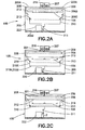
- the substrate aligner apparatus 105 generally comprises a frame 205, an inverted chuck 206, an inverted chuck drive section 216 and drive system 207, a sensing device 209, a substrate transfer mechanism 210, and a transfer mechanism drive section 211 and drive system 222.
- the frame 205 may have an opening, aperture or slot 213.
- Substrate transporter 103 (See Fig. 1 ) transports a substrate 212 (held on the transport end effector 106) into and out of the frame 205. Opening 213 thus allows the end effector 106 access to the substrate aligner apparatus 105.
- the inverted chuck 206 may be located proximate to the top 205A of frame 205.
- the chuck may have a span member 206A and downward extensions 206B depending therefrom.
- the span member 206A and downward extensions 206B are looped above the substrate 212 and transporter end effector 106 when located within the frame 205.
- the span member 206A mates the chuck 206 to the drive section 216 of drive system 207 as will be described below.
- the span member 206A faces the top side of the substrate 212 while the downward extension members 206B extend downward from the span member 206A.
- Each downward extension member 206B has rest pads 206C for supporting substrate 212 when held by the chuck 206.
- Each extension member 206B extends down sufficiently from the span member 206A so that the rest pads 206C thereon are positioned to contact the peripheral edge of substrate 212 along the bottom side of the substrate 212 when the chuck 206 holds substrate 212.
- the downward extension members 206B reach around opposite sides of the substrate 212 from the span member 206A, from above the substrate, to engage the bottom region of the peripheral edge of the substrate 212.
- chuck 206 is referred to herein as an inverted chuck.
- the rest pads 206C may be passive rest pads or alternatively, rest pads 206C may actively grip the substrate 212. In alternate examples the chuck may have any other suitable configuration.
- the inverted chuck drive system 207 is a rotary drive system located at the top 205A of the frame 205 and is mated with the inverted chuck 206 through drive section 216.
- Examples of motors that may be used in drive system 207 include stepper motors and servo motors'.
- the motors may be brushless and may have an encoder to coordinate the alignment of substrate 212 with a signal transmitted by an optical sensor 209 corresponding to the detection of the wafer fiducial 220.
- the chuck drive system 207 is independent from the substrate transfer mechanism drive system 222. In alternate examples the chuck drive system 207 may be any other suitable configuration.
- the substrate aligner apparatus 105 has a contamination shield 208.
- the contamination shield 208 is located near the top 205A of frame 205, between the drive section 216 of drive system 207, as well as the rotatable span portion 206A over the substrate, and the substrate 212 when the substrate is held by chuck 206.
- the shield 208 may be generally flat in shape and of a diameter such that it fits within the chuck 206, yet shields the entire substrate, when the chuck 206 is holding a 200mm or 300mm substrate 212.
- the shield may be fixed relative to the frame 205.
- the shield 208 is attached to the frame so as not to interfere with rotation of the inverted chuck 206.
- the shield 208 may be supported from a post 221 extending concentrically through the drive shaft 216 driving chuck 206.
- the shield may be made of any suitable material such as metal or plastic and may have any desired planform shape, such as substantially circular. In alternate examples the shield 208 may be of any other suitable configuration.
- the aligner 105 has a sensing device 209 for detecting the substrate fiducial 220.
- the sensing device 209 is a reflective optical sensor.
- the sensor 209 may be any other suitable sensing device including capacitive and inductive sensors.
- sensing device 209 may be mounted on contamination shield 208.
- the sensor 209 may be mounted in any other suitable manner so that the substrate 212, when held by the chuck 206, is in the sensing field of the sensor 209 and rotation of the inverted chuck 206 is unrestrained by the sensor 209 and its mount.
- Sensor 209 is positioned radially from the center of the chuck's 206 axis of rotation so that the peripheral edge of substrate 212 and its fiducial 220 are disposed in registry with the sensor 209 and so that the rotating chuck structure does not obstruct the sensing of the fiducial 220.
- Sensing device 209 may also be fixed from movement relative to the frame 205. In alternate examples the sensing device may have any other desired configuration.
- the substrate transfer mechanism 210 of this example is located under the chuck 206 in order to pick substrate 212 from the chuck and place the substrate 212 on the end effector 106.
- the transfer mechanism 210 may have multiple independently actuated lifters. Two lifters 210A, 210B are shown in Fig. 3 (In Figs. 2A-2C , only one of the lifters 210A, 210B is shown for illustrative purposes). In alternate examples, the transfer mechanism 210 may have any number of lifters.
- each of the two lifters are similar in configuration and have span members 210AS, 210BS and upward extensions 210AC, 210BC depending from opposite ends of the lifter span members 210AS, 210BS.
- the span members 210AS, 210BS mate the lifters 210A, 210B with the substrate transfer mechanism drive section 211 of the drive system 222 as described below.
- the span members 210AS, 210BS face the bottom of the substrate 212 when substrate 212 is held by chuck 206 while each of the upward extensions 210C extend up towards the bottom of substrate 212 when substrate 212 is held by chuck 206.
- Each of the upward extensions 210C has rest pads 219 for supporting substrate 212. Each rest pad 219 contacts the bottom peripheral edge of substrate 212.
- the substrate transfer mechanism 210 may have any other suitable configuration.
- the substrate transfer mechanism drive system 222 is located at the bottom 205B of the frame 205.
- the drive system 222 is mated to the transfer mechanism 210 through drive section 211.
- drive system 222 is a linear drive system capable of independently moving each lifter 210A, 210B back and forth along drive Axis Z (See Figs. 2A-2C ).
- Drive system 222 may for example be a ball-screw drive, a rod linear actuator or a slide linear actuator. In alternate examples drive system 222 may be of any other suitable configuration or drive type.
- the linear travel of the drive system 222 is sufficient for either lifter 210A, 210B to lift substrate 212 off chuck 206 when substrate 212 is held by chuck 206 and lower it onto end effector 106.
- the substrate transporter end effector 106 enters the aligner above the chuck rest pads 206C through the opening in the frame 213 and places the substrate within the chuck 206 (See Fig. 2A ).
- the end effector moves down below the chuck 206 thereby placing the substrate 212 onto the inverted chuck rest pads 206C, (See Block 502 of Fig. 7 and Fig. 2B ).
- the end effector 106 if desired may remain extended between the inverted chuck 206 and transfer mechanism lifters 210A, 210B.
- the substrate transporter end effector 106 is able to remain within the frame 205 during alignment due to the configuration of the chuck 206 and transfer mechanism 210 as shown in Figs. 2A-2C .
- the inverted chuck 206 grips the substrate 212 positioned thereon for alignment.
- the inverted chuck 206 is rotated, via the inverted chuck drive section 216 and drive system 207 (See Block 503 of Fig. 7 ).
- the sensing device 209 senses the peripheral edge of the substrate 212 and detects the substrate alignment feature (fiducial) 220 on the edge of the substrate 212 as may be realized.
- the contamination shield 208 prevents any particles generated by the chuck 206 and chuck drive system 207, 216 from contaminating the surface of the substrate 212.
- Sensing device 209 is able to detect the substrate fiducial 220 independent of its orientation relative to the gripping pads of chuck 206.
- the chuck rest pads 206C grip the edge of the substrate 212, without masking the edge of its fiducial 220 and hence the fiducial 220 and wafer edge are always substantially exposed to sensing device 209.
- sensing device 209 is capable of detecting the fiducial 220 from but one side (e.g. the top) of the substrate 212 so that obstructions or cover on the opposite side of the wafer does not degrade sensor performance. Detection of the substrate edge and fiducial 220 independent of position on the chuck 206 eliminates substrate placement re-tries on the chuck 206.
- a suitable indication signal is transmitted to a controller (not shown) to register the position of the substrate fiducial 220 relative to a desired reference frame.
- the sensing device 209 may also send suitable signals to the controller enabling the controller to determine substrate eccentricity with respect to a desired substrate center reference location.
- the controller may calculate chuck movement to achieve desired alignment orientation of the substrate 212 and send movement commands to drive 207.
- the inverted chuck 206 positions the substrate 212 to a desired alignment orientation (See Block 503 of Fig. 7 ).
- the appropriate lifting pad 210A, 210B is then selected to lift the post aligned substrate 212 off of the inverted chuck 206 (See Block 504 of Fig. 7 ).
- the lifting pads 210A, 210B are independently actuated and because of their configuration (See Fig. 3 ), at least one of the lifting pads 210A, 210B is capable of clearing obstructions from end effector structure and chuck structure regardless of chuck 206 orientation post substrate positioning to pick the post positioned substrate 212 from the chuck 206.
- transfer mechanism 210 can access the inverted chuck independent of the position of the substrate transporter end effector 106 within the aligner frame 205 and without rotationally repositioning the substrate 212 on the chuck 206.
- the lifting pads 210A, 210B lift the substrate 212 from the inverted chuck 206 and the inverted chuck 206 may return to its home position (See Blocks 504-505 of Fig. 7 ).
- the substrate transporter end effector 106 picks the substrate off the lifting pad 210A, 210B, grips the wafer (substrate) 212 and delivers the substrate 212 to be processed further (See Blocks 506-507 of Fig. 7 ). It is noted that the controller may position the end effector 106 so that picking the substrate from the lifting pads 210A, 210B also effects correction of eccentricity misalignment.
- Table 2 below summarizes the exemplary process described above (as graphically depicted in Fig. 7 ) and illustrates at a glance the improved efficiencies provided over conventional aligners. Table 2 also identifies exemplary times corresponding to each of the operations performed to align a substrate using this example.
- the aligner 105 in the example shown in Figs. 2A-3 and Fig. 7 is capable of significantly reducing the alignment time to align a substrate over the at least eleven second alignment time of the prior art as described in the background section above.
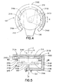
- the substrate aligner apparatus 105' generally comprises a frame (not shown), a rotatable sensor head 318 with at least one sensing device 317, and a substrate support 319.
- the frame (not shown) is similar to the frame 205 (See Figs. 2A-2C ) in the first embodiment of the substrate aligner apparatus 105 described before unless otherwise noted.
- the rotatable sensor head 318 has a base member 318A located, for example, towards the bottom of the frame and below the end effector 106 when the end effector 106 is inside the frame.
- the end effector 106 may access the frame through an opening similar to opening 213 in Figs. 2A-2C .
- the base member 318A is connected to a drive section 321 of the sensor head drive system (not shown) as will be described below.
- the base member 318A extends radially from the rotatable sensor head's 318 axis of rotation, Axis Z, as shown in Fig. 5 .
- Base member 318A has a base extension member 318B depending therefrom on but one side of the base member 318A in this embodiment.
- the base extension member 318B extends upward toward the top of the frame from base member 318A above the substrate 212 when held by the substrate support 319.
- Base extension member 318B has a span member 318C depending therefrom.
- Span member 318C may be arcuate in shape and extends above substrate 212 to the opposite side from the base extension member 318B. As seen best in Fig. 4 , the arcuate shape of span member 318C leaves a distance between the perimeter of the substrate 212 and span member 318C so that the span member 318C does not overhang the substrate 212. In alternate embodiments the span member 318C may have any other desired shape. As seen in Fig. 5 , the span member 318C has a downward extension member 318D depending therefrom on the side opposite the base extension member 318B. Thus, as best shown in Fig.
- the base extension member 318B, the span member 318C and the downward extension member 318D wrap around the substrate support 319 and the substrate 212 from the base member 318A.
- the rotatable sensor head 318 also has substrate rest pads 316A, 316B located on opposite sides of the sensor head 318. Substrate rest pads 316A depend from the downward extension member 318D while substrate rest pads 316B depend from the base extension member 318B as shown in Figs. 4 and 5 .
- Substrate rest pads 316A, 316B wrap around the underside of substrate 212 from the downward extension member 318D and the base extension member 318B so that the substrate rest pads 316A, 316B contact the bottom peripheral edge of substrate 212 when substrate 212 is held by the sensor head 318 as will be described below.
- the substrate rest pads 316A, 316B may be passive or active gripping. In alternate embodiments the rotatable sensor head 318 may have any other desired configuration.
- sensor head 318 may have two sensing devices 317A, 317B located on opposite sides of sensor head 318 as shown in Figs. 4 and 5 .
- the sensor head 318 may have more or less than two sensors.
- Sensing devices 317A, 317B may be reflective optical sensors or through beam optical sensors.
- the sensing devices 317A, 317B may be capacitive or inductive sensing devices.
- Sensors 317A, 317B are radially positioned from the center of rotation, Axis Z, a sufficient distance so that the sensors 317A, 317B are capable of sensing the peripheral edge of substrate 212.
- the sensor head drive system (not shown) is mated to the sensor head through drive section 321 and is similar to the rotary drive described before with respect to aligner 105. However, in this embodiment the drive system is located at the bottom of the frame and rotates the sensor head around Axis Z as shown in Fig. 5 . In alternate embodiments the drive system may be of any other desired configuration.
- the substrate support 319 in this exemplary embodiment is nested between the sensor head span member 318C and the sensor head base member 318A.
- the substrate support system has a span member 319A whose center is located substantially coincident with Axis Z and mated to a substrate support drive member 322, also located along Axis Z.
- Substrate support drive member 322 is part of the substrate support drive system (not shown) as described below.
- the span member 319A has two upward extension members 319B depending on opposite sides therefrom. In alternate embodiments there may be any number of upward extension members depending from the span member 319A.
- the span member 319A faces the bottom of the substrate 212 when held by the support 319.
- the upward extension members 319B have support pads 320A, 320B that overlap at least in part the sensor head devices 317A, 317B of sensor head 318 (See Fig. 5 ).
- the substrate support pads 320A, 320B are configured to support the bottom peripheral edge of substrate 212. Rest pads 320A, 320B may actively or passively grip substrate 212.
- Support pads 320A, 320B or at least a portion thereof in way of sensor devices 317A, 317B may also be made of a transparent material so that a beam A,B of radiation from sensors 317A, 317B, capable of detecting the edge of the substrate 212 when seated on support pads 320A, 320B, passes through the portion of the support pads 320A, 320B in way of beam A,B to the sensor receiver (not shown) so as to be able to detect the edge of the substrate 212 and the fiducial 220 on the edge.
- the material for the support pads 320A, 320B may for example be quartz, optically transparent to light beams, or any other suitable material.
- the support pads 320A, 320B may be of a non-transparent material.
- the substrate support 319 may have any other desired configuration.
- the substrate support drive system (not shown) is similar to the linear drive system 211, 222 described before and shown in Figs. 2A-2C , unless otherwise noted.
- the substrate support drive system mates with the substrate support 319 through the substrate support drive member 322.
- the substrate support drive system in this embodiment transfers the substrate 212 back and forth along Axis Z.
- the drive system is capable of moving the substrate support 319 from a position where the support pads 320A, 320B are located above sensor head rest pads 316A, 316B (See Fig. 5 ) to a position where the support pads 320A, 320B are below sensor head rest pads 316A, 316B.
- the substrate support is not capable of rotation but in alternate embodiments the substrate support drive system may be combined with a rotational drive so that the substrate support system not only travels along Axis Z but rotates about Axis Z as well.
- the substrate transporter end effector 106 enters the aligner between the sensor head span member 318C and sensor head substrate rest pads 316A, 316B through the opening in the frame (similar to opening 213 in Fig. 2A ) (See Block 601 in Fig. 8 ) and places the substrate on the support pads 320A, 320B of substrate support 319 about Axis Z.
- the substrate support 319 may move up along Axis Z to the position shown in Fig. 5 to enable the end effector 106 to place substrate 212 onto the substrate support pads 320A, 320B (See Block 602 in Fig.
- the end effector 106 may move down along Axis Z, to a position below support pads 320A, 320B and above the support system span member 319A so that its location is within substrate support 319 as best shown in Fig. 5 .
- the end effector 106 may remain extended under the substrate 212.
- the rotatable sensor head 318 is rotated more than one-hundred and eighty degrees, either clockwise or counter clockwise (as indicated by arrows R in Fig. 4 , so that the entire peripheral edge of substrate 212 is scanned by sensing devices 317A, 317B.
- the fiducial 220 can be detected by the sensing devices 317A, 317B independent of the fiducial 220 location relative to the support pads 320A, 320B of substrate support 319.
- the fiducial 220 is not masked from the sensor beam because substrate support pads 320A, 320B, at least in way of the beam, are transparent to the sensor beam thereby allowing the beam to pass through the support pads 320A, 320B and impinge on the substrate edge to enable sensors 317A, 317B to sense the fiducial.
- a suitable indication signal is transmitted from the sensor to a controller (not shown) to register the detection of the substrate alignment feature 220.
- the substrate 212 is lowered by substrate support 319 onto the sensor head substrate rest pads 316A, 316B thereby transferring the substrate 212 from the substrate support 319 to the rotatable sensor head 318 (See Block 604 in Fig. 8 ).
- the end effector 106 may remain below the sensor head rest pads 316A, 316B.
- the rotatable sensor head 318 rotates substrate 212 to a desired alignment orientation in accordance with instruction from the controller (See Block 605 in Fig. 8 ).
- the rotation of the sensor head 318 is significantly faster during the scanning operation in Block 603 of Fig. 8 than it is in the substrate orientation operation in Block 605 of Fig. 8 .
- the increased rotational speed of the sensor head 318 is accomplished, for example, where the sensor head drive system is a multiple speed rotary drive such as multiple speed stepper motor. In alternate embodiments, any suitable drive system may be used.
- the substrate transporter end effector 106 lifts the substrate 212 off the sensor head rest pads 316A, 316B, grips the substrate 212 and delivers the substrate 212 to be processed further (See Block 606 in Fig. 8 ).
- the substrate support 319 can lift substrate 212 from the sensor head rest pads 316A, 316B.
- Substrate support 319 has support pads 320A, 320B that are positioned to clear the sensor head rest pads 316A, 316B in the event that the sensor head rest pads 316A, 316B block the pick path of the end effector. Further, as seen in Fig. 5 , the substrate support pads 320A, 320B are positioned as to not interfere or obstruct end effector 106 motion along Axis Z. Accordingly, transfer of the substrate 212, post positioning, to the end effector may be accomplished independent of substrate orientation and without rotational repositioning of the substrate. The sensor head moves to its home position.
- the substrate aligner apparatus generally comprises a frame (not shown), a rotatable sensor head 423 with sensing device 424 and a rotatable chuck 425 having a buffer system 440 for buffering substrates.
- the frame in this example is similar to frame 205 described before and shown in Figs. 2A-2C unless otherwise noted.
- the rotatable sensor head 423 may be rotatable about Axis Z.
- the sensor head 423 has a base section 423A mated with a sensor head drive section (of which only a portion of shaft 430 is shown in Fig. 6 ).
- the sensor head drive shaft 430 is connected to a sensor head drive system (not shown) as described below.
- base member 423A has arms 423B, 423C extending radially from its center of rotation disposed at Axis Z.
- Base member 423A has an upward extension member 423D depending from one arm 423C of base member 423A. In alternate examples both arms may have upward extension members depending therefrom.
- the upward extension member 423D has cantilever members 423E depending from the upward extension member 423D for supporting the sensing device 424.
- the sensing device 424 may be a through beam optical sensor having, for example, a beam transmitter and a beam detector on the cantilevered member 423E.
- the sensing device may also be a reflective sensor, a capacitive sensor or an inductive sensor.
- the sensing device 424 is positioned radially from Axis Z at a distance that enables the sensing device 424 to scan the peripheral edge of substrate 212 and detect the fiducial when substrate 212 is held by the substrate buffering system 425.
- the sensor head drive system (not shown) mates to the rotatable sensor head base member 423A through drive shaft 430.
- the sensor head drive system may be similar to the rotational drive systems in aligners 105, 105' as described before, but with motors for independent rotation of co-axial shafts 430, 431.
- the sensor head drive system may be located at any suitable location on the frame and provides rotation about Axis Z.
- chuck 425 is rotatable about Axis Z.
- the chuck 425 has a base member 425A that is substantially centered with Axis Z and is mated to a chuck drive of which only a portion of shaft 431 is shown in Fig. 6 .
- the drive shaft 431 is co-axial with shaft 430 and rotates about Axis Z.
- the drive section is capable of independent rotation of shafts 430, 431.
- the base member 425A has arms 425B, 425C extending radially from the center of rotation, Axis Z. Each arm 425B, 425C has a rest pad system 425D depending upwardly therefrom.
- each rest pad system 425D has two rest pad extension members 425E, 425F.
- Each rest pad extension member 425E, 425F has a generally stepped shape with horizontal sections 425G, 425H forming rest pads.
- One set of rest pads 425G form support for substrate 212 being scanned while the other set of rest pads 425H forms buffer 440.
- the rest pads 425G, 425H can be active or passive gripping and may be made of transparent or non-transparent material depending on the sensing device being used as described before with reference to pads 320A, 320B shown in Fig. 5 .
- rest pads 425G, 425H may be made of quartz or other suitable material transparent to light beam L generated by sensor 424.
- the rest pads 425G, 425H are at a radial distance from Axis Z, sufficient to hold substrate 212 on its bottom peripheral edge while at the same time allowing the edge of substrate 212 to be scanned by the sensing device 424.
- the rest pads 425G, 425H and the cantilever members 423E of the sensor head are vertically spaced to allow a substrate transporter end effector 106 to access the rest pads 425G in order to pick or place a substrate on the rest pads.
- the rest pad extension members 425D do not rotationally interfere with the cantilever members 423E.
- Rest pads 425G are positioned to pass between cantilever members 423E.
- Rest pads 425H are positioned to pass under the lower most cantilever member 423E.
- a substrate transporter with a single end effector such as those described in U.S. Patent 5,765,983 and U.S. Patent 5,577,879 , may be used with this exemplary example.
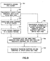
- the substrate transporter end effector 106 enters the aligner above the chuck or buffering system rest pads 425G through the frame opening (similar to opening 213 shown in Fig. 2A ) and places a first substrate, similar to substrate 212, onto rest pads 425G (See Blocks 701, 702 in Fig. 9 ).
- the empty end effector/substrate transporter may retract out of the aligner.
- movements of the empty end effector may be conducted at greater speed than when holding a substrate.
- the end effector/substrate transporter may retrieve a second substrate for alignment (See block 705 in Fig. 9 ).
- the upper rest pads 425G form scanning rest pads while lower rest pads 425H form buffer rest pads.
- the rotatable sensor head 423 in Block 703 of Fig. 9 , is rotated by the sensor head drive shaft 430 to allow the sensing device 424 to detect the fiducial of the first substrate placed on the upper pads 425G.
- Sensing device 424 can detect the fiducial independent of its placement on the chuck pads 425G. For example, even if the fiducial is resting on one of the rest pads 425G, the transparent material of the rest pads in way of the sensor through beam leaves the fiducial unmasked or sensable to the beam of the sensor 424. Also, the rest pads 425G grip the substrate on its edges leaving the upper surface of the substrate exposed, allowing, in an example where the sensor is a reflective, capacitive or inductive sensor, fiducial detection without any obstruction from the chuck 425 structure.
- a suitable indication signal is transmitted to a controller (not shown) to register the detection of the substrate alignment feature.
- the chuck 425 then rotates the substrate to a desired alignment orientation (See Block 704 in Fig. 9 ).
- rotation of the sensor head 423 to scan the substrate and detect the fiducial may be performed at a much higher rate of rotation than chuck rotation to position the substrate.
- the substrate transporter/end effector 106 may enter the frame (See Block 705 in Fig. 9 ) in the same manner described above at a position above the buffer rest pads 425H to buffer a second substrate on rest pads 425H.
- the transporter moves an empty end effector (that may be the same end effector having buffered the second substrate or another empty end effector) up to a position between the first and second substrates as they are held in the chuck 425.
- the end effector moves to a location under the first substrate held on pads 425G and picks the positioned substrate from pads 425G for further processing (See Block 706 in Fig. 9 ).
- the substrate on the buffer pads 425H, or a new substrate if desired may be placed on the upper pads 425G of the chuck 425.
- the rest pad extension members 425D may be movable to allow vertical movement of the end effector when transferring the buffered substrate to the upper rest pads without the end effector partially retracting out of the aligner. After placement of the second substrate onto pads 425G, the process in Blocks 703-704 is repeated. As may be realized, the buffer on chuck 425 increases the efficiency of the aligner by minimizing transfer times for loading the aligner.
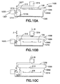
- FIG. 10A-10C there is shown another substrate aligner apparatus 1105 in accordance with still yet another example.
- the aligner apparatus 1105 is respectively shown in Figs. 10A-10C in three different positions.
- the aligner apparatus 1105 in this exemplary embodiment is generally similar to the aligner apparatus 105 described before and shown in Figs. 2A-2C , except as otherwise noted. Similar features are thus similarly numbered.
- Aligner apparatus 1105 has a movable chuck 1206, a sensing device 1209 and a substrate transfer system 1210.
- the aligner 1105 also has a drive system 1207 powering the movements of the movable chuck 1206.
- the transfer system 1210 is configured for holding the substrate 2112 in a fixed position inside the aligner.
- the substrate transfer system 1210 has members 1210A that are fixed to the aligner frame 1205 in any suitable manner or position.
- the transfer system members 1210A may have any suitable configuration, and are provided with substrate rest pads 1219 (similar to rest pads 219 shown in Fig. 3 ). Rest pads 1219, in this example, are not movable but may provide a substrate placement position used when scanning the substrate with sensing device 1209, as will be described further below.
- Movable chuck 1206, has a general inverted chuck configuration (similar to chuck 206 shown in Fig. 2A-2C ). In this example, chuck 1206 is movable both vertically (in the direction indicated by arrow Z in Fig. 10b ) and is rotatable about axis or rotation ⁇ .
- the drive system 207 has rotatable drive 1216 and linear drive sections 1222 connected by a transfer member 1207T as shown in Fig. 10A .
- Linear drive 1222 similar to linear drive 222 shown in Figs. 2A-2C , is operably coupled to transfer member 1207T, and is capable of traversing the transfer member 1207T in the Z direction relative to the aligner frame.
- the transfer member 1207T may have any suitable shape (the configuration shown in Figs. 10A-10C is merely exemplary) and may be movably mounted to the aligner frame 1205 in any desired manner to allow relative movement between transfer member and frame in the Z direction. As seen in Fig.
- the movable chuck 1206 is mounted to the transfer member 1207T, and thus moves vertically (relative to the frame 1205) in unison with the transfer member.
- Chucking may be rotatably mounted relative to the transfer member 1207T (such as by suitable rotatable bearing or bushing system) so that chuck 1206 may rotate relative to the transfer member and the aligner frame about axis ⁇ .
- Rotatable chuck 1206 is rotated about axis ⁇ under impetus from rotational drive section 1216 coupled to the chuck 1206 by a suitable rotational drive transmission system (e.g. rotational drive shaft).
- rotational drive section 1216 may also be borne by the movable transfer member 1207T.
- the rotational drive may be mounted to the aligner frame and coupled to the rotatable chuck by a suitable transmission capable of transmitting rotation to the chuck and accommodating linear motion of the chuck relative to the aligner frame.
- the sensing device 1209 that is similar to sensing device 209 shown in Fig. 2A-2C ) is mounted on chuck 1206 as shown in Fig. 10A .
- Sensing device 1209 is positioned to sense the peripheral edge of substrate 212, and its fiducial, when the substrate 212 is seated on the rest pads 1219 of transfer system 1210.
- Sensing device 1219 is capable of detecting the fiducial 220 (see Fig. 3 ) of the substrate independent of the orientation of the substrate 212 and position of the fiducial relative to rest pads 1219 or any other structure of the transfer system 1210.
- substrate alignment may be in the following exemplary manner.
- Substrate 212 introduced into the aligner 1105 with end effector 106, may be positioned onto stationary transfer system rest pads 1219 (see Figs. 10A-10B ). Scanning of the substrate 212, for fiducial detection, as well as eccentricity measurements if desired, may be performed by rotating chuck 1206 (about axis ⁇ ), thereby rotating the sensor device 1209 relatively to stationary substrate and scanning the entire periphery of the substrate. As seen in Fig. 10B , in this position (i.e.
- the movable chuck 1206 has a vertical position so that the chucks substrate rest pads 1206C (similar to substrate rest pads 206C described before) are located below the rest pads 1219 of transfer system 1210 supporting the substrate 212 after location of the fiducial 220 is identified, for example as described above by detection with sensor 1209 alignment of the substrate is effected with movable chuck 1206.
- the chuck 1206 is moved in the Z direction to pick the substrate (from the transfer system rest pads) with the substrate 212 resting on chuck resting pads 1206, now positioned above the resting pads 219 of the transfer system (see Fig. 10C ), the chuck is rotated about axis ⁇ to place the substrate in the desired alignment.
- the end effector 106 may pick the aligned substrate from the rest pads 1206C of the chuck 1206.
- the chuck 1206 may be moved to place the substrate on the rest pads 1219 of transfer system 1210 (similar to the position shown in Fig. 10B ) the end effector picks the substrate 212 from the transfer system 1210.
- the end effector may be performed without rotational repositioning of the substrate.
- the end effector may remain extended throughout the alignment process.
- the previously described examples of the aligner 105, 105', 105", and 1105 have many advantages over conventional aligners. Some of the advantages of the aligners 105, 105', 105" and 1105 include but are not limited to the following; elimination of robot re-tries in placing the wafer in the aligner.
- the wafer may be arbitrarily oriented relative to the end effector without the chuck ever being on the pick path of the robot end effector.
- the wafer may be aligned properly, without robot re-tries, even for the case when the fiducial lies on top of the aligner chuck pads.
- the align times of the present invention are significantly shorter than the align times of conventional aligners.
- the wafer may always be moved by edge contact without rolling or slipping relative to the chuck, therefore yielding minimum particle generation.
- the robot end effector may stay positioned under the aligner and substrate without any mechanical interference during the alignment process. This means that the wafer may be aligned and placed on the robot end effector with one extend and one retract motion from the aligner station.
- only one wafer lift is employed in order to allow the wafer to be picked at the desired post-positioning orientation. Multiple vertical moves are eliminated. This yields minimum wafer walking and optimal aligner throughput.
Landscapes
- Engineering & Computer Science (AREA)
- Physics & Mathematics (AREA)
- General Physics & Mathematics (AREA)
- Manufacturing & Machinery (AREA)
- Condensed Matter Physics & Semiconductors (AREA)
- Computer Hardware Design (AREA)
- Microelectronics & Electronic Packaging (AREA)
- Power Engineering (AREA)
- Human Computer Interaction (AREA)
- Automation & Control Theory (AREA)
- Container, Conveyance, Adherence, Positioning, Of Wafer (AREA)
Applications Claiming Priority (2)
| Application Number | Priority Date | Filing Date | Title |
|---|---|---|---|
| US11/093,479 US7891936B2 (en) | 2005-03-30 | 2005-03-30 | High speed substrate aligner apparatus |
| PCT/US2006/011400 WO2006105156A2 (en) | 2005-03-30 | 2006-03-29 | High speed substrate aligner apparatus |
Publications (3)
| Publication Number | Publication Date |
|---|---|
| EP1866958A2 EP1866958A2 (en) | 2007-12-19 |
| EP1866958A4 EP1866958A4 (en) | 2010-04-21 |
| EP1866958B1 true EP1866958B1 (en) | 2014-06-25 |
Family
ID=37054057
Family Applications (1)
| Application Number | Title | Priority Date | Filing Date |
|---|---|---|---|
| EP06748850.2A Active EP1866958B1 (en) | 2005-03-30 | 2006-03-29 | High speed substrate aligner apparatus |
Country Status (7)
| Country | Link |
|---|---|
| US (2) | US7891936B2 (zh) |
| EP (1) | EP1866958B1 (zh) |
| JP (2) | JP5820559B2 (zh) |
| KR (1) | KR101366754B1 (zh) |
| CN (2) | CN101379604B (zh) |
| TW (1) | TWI429013B (zh) |
| WO (1) | WO2006105156A2 (zh) |
Families Citing this family (10)
| Publication number | Priority date | Publication date | Assignee | Title |
|---|---|---|---|---|
| US8545165B2 (en) | 2005-03-30 | 2013-10-01 | Brooks Automation, Inc. | High speed substrate aligner apparatus |
| US7891936B2 (en) | 2005-03-30 | 2011-02-22 | Brooks Automation, Inc. | High speed substrate aligner apparatus |
| JP2008103544A (ja) * | 2006-10-19 | 2008-05-01 | Yaskawa Electric Corp | アライナー装置 |
| CN103192463A (zh) * | 2012-01-05 | 2013-07-10 | 沈阳新松机器人自动化股份有限公司 | 透光夹持式预对准机 |
| WO2014197537A1 (en) * | 2013-06-05 | 2014-12-11 | Persimmon Technologies, Corp. | Robot and adaptive placement system and method |
| US9062968B2 (en) | 2013-07-23 | 2015-06-23 | Avago Technologies General Ip (Singapore) Pte. Ltd. | PCB loading apparatus for measuring thickness of printed circuit board stack |
| US20150090295A1 (en) * | 2013-09-28 | 2015-04-02 | Applied Materials, Inc. | Apparatus and methods for a mask inverter |
| CN107407830B (zh) * | 2015-01-28 | 2020-11-06 | 堺显示器制品株式会社 | 翻转装置和液晶显示面板的制造方法 |
| WO2017011581A1 (en) * | 2015-07-13 | 2017-01-19 | Brooks Automation, Inc. | On the fly automatic wafer centering method and apparatus |
| KR102501318B1 (ko) * | 2022-04-07 | 2023-02-16 | 양희찬 | 웨이퍼 이동암 |
Family Cites Families (41)
| Publication number | Priority date | Publication date | Assignee | Title |
|---|---|---|---|---|
| US4915564A (en) | 1986-04-04 | 1990-04-10 | Materials Research Corporation | Method and apparatus for handling and processing wafer-like materials |
| US5102280A (en) * | 1989-03-07 | 1992-04-07 | Ade Corporation | Robot prealigner |
| US5264787A (en) * | 1991-08-30 | 1993-11-23 | Hughes Aircraft Company | Rigid-flex circuits with raised features as IC test probes |
| JPH06151566A (ja) * | 1992-11-04 | 1994-05-31 | Matsushita Electric Ind Co Ltd | オリフラ位置検出装置およびオリフラ位置合わせ装置 |
| US5491618A (en) | 1993-08-20 | 1996-02-13 | Lights Of America, Inc. | Light fixture |
| JPH07260455A (ja) * | 1994-03-23 | 1995-10-13 | Kokusai Electric Co Ltd | 基板位置決め方法及び装置 |
| US5568969A (en) | 1996-03-22 | 1996-10-29 | Yu; Jack | Convertible light assembly |
| JP3439607B2 (ja) | 1996-09-04 | 2003-08-25 | 東京エレクトロン株式会社 | ノッチ整列装置 |
| US6126381A (en) * | 1997-04-01 | 2000-10-03 | Kensington Laboratories, Inc. | Unitary specimen prealigner and continuously rotatable four link robot arm mechanism |
| US6126380A (en) * | 1997-08-04 | 2000-10-03 | Creative Design Corporation | Robot having a centering and flat finding means |
| US6530732B1 (en) | 1997-08-12 | 2003-03-11 | Brooks Automation, Inc. | Single substrate load lock with offset cool module and buffer chamber |
| US6309163B1 (en) * | 1997-10-30 | 2001-10-30 | Applied Materials, Inc. | Wafer positioning device with storage capability |
| US6439740B1 (en) | 1997-12-01 | 2002-08-27 | Technical Consumer Products, Inc. | Lighting fixture having a screw lock lamp support |
| JP2000021956A (ja) * | 1998-07-02 | 2000-01-21 | Mecs Corp | ノッチ合わせ機 |
| JP2000068357A (ja) * | 1998-08-25 | 2000-03-03 | Kobe Steel Ltd | ウェーハ切欠部位置検出装置及びウェーハ特性測定装置 |
| US6212961B1 (en) * | 1999-02-11 | 2001-04-10 | Nova Measuring Instruments Ltd. | Buffer system for a wafer handling system |
| IL128087A (en) * | 1999-01-17 | 2002-04-21 | Nova Measuring Instr Ltd | Buffer station for a wafer handling system |
| US6275742B1 (en) | 1999-04-16 | 2001-08-14 | Berkeley Process Control, Inc. | Wafer aligner system |
| US6357996B2 (en) * | 1999-05-14 | 2002-03-19 | Newport Corporation | Edge gripping specimen prealigner |
| EP1139390A1 (en) * | 2000-03-28 | 2001-10-04 | Infineon Technologies AG | Semiconductor wafer pod |
| US6468022B1 (en) | 2000-07-05 | 2002-10-22 | Integrated Dynamics Engineering, Inc. | Edge-gripping pre-aligner |
| CN100398272C (zh) * | 2000-09-01 | 2008-07-02 | 阿赛斯特技术公司 | 具有缓冲性能的边缘夹持校准器 |
| US6435807B1 (en) * | 2000-12-14 | 2002-08-20 | Genmark Automation | Integrated edge gripper |
| US6494589B1 (en) | 2001-08-31 | 2002-12-17 | Shing Jy Shyu | Ceiling fan having one or more changeable lamp devices |
| JP2003163258A (ja) * | 2001-09-14 | 2003-06-06 | Assist Japan Kk | ウェハのアライナー装置 |
| US20030053904A1 (en) * | 2001-09-14 | 2003-03-20 | Naofumi Kirihata | Wafer aligner |
| US7119566B2 (en) | 2002-03-22 | 2006-10-10 | Electro Scientific Industries, Inc. | Test probe alignment apparatus |
| JP3956350B2 (ja) * | 2002-03-25 | 2007-08-08 | 東京エレクトロン株式会社 | 位置決め機能を有する基板処理装置及び位置決め機能を有する基板処理方法 |
| US6669159B1 (en) | 2003-01-07 | 2003-12-30 | Dong Guan Bright Yin Huey Lighting Co., Ltd. | Ceiling fixture |
| JP2004259845A (ja) * | 2003-02-25 | 2004-09-16 | Nikon Corp | パラメータ調整方法、物体搬送方法、露光装置、及びプログラム |
| JP4277092B2 (ja) * | 2003-03-28 | 2009-06-10 | アシストテクノロジーズジャパンホールディングス株式会社 | ウェハのアライナー装置 |
| KR101015778B1 (ko) * | 2003-06-03 | 2011-02-22 | 도쿄엘렉트론가부시키가이샤 | 기판 처리장치 및 기판 수수 위치의 조정 방법 |
| US7596425B2 (en) * | 2003-06-13 | 2009-09-29 | Dainippon Screen Mfg. Co., Ltd. | Substrate detecting apparatus and method, substrate transporting apparatus and method, and substrate processing apparatus and method |
| US7019817B2 (en) * | 2003-07-14 | 2006-03-28 | Kawasaki Jukogyo Kabuishiki Kaisha | Edge-holding aligner |
| KR100547936B1 (ko) | 2003-08-07 | 2006-01-31 | 삼성전자주식회사 | 불순물 용출 장치 |
| US20050099817A1 (en) | 2003-11-10 | 2005-05-12 | Lin Kuo K. | Ceiling fixture |
| US20060007176A1 (en) | 2004-07-06 | 2006-01-12 | Chung-Yi Shen | Input method and control module defined with an initial position and moving directions and electronic product thereof |
| KR100657789B1 (ko) | 2004-07-15 | 2006-12-14 | 삼성전자주식회사 | 유전막의 누설 전류 특성을 검사하는 방법 및 이를수행하기 위한 장치 |
| US7891936B2 (en) | 2005-03-30 | 2011-02-22 | Brooks Automation, Inc. | High speed substrate aligner apparatus |
| US8545165B2 (en) | 2005-03-30 | 2013-10-01 | Brooks Automation, Inc. | High speed substrate aligner apparatus |
| US9099506B2 (en) | 2005-03-30 | 2015-08-04 | Brooks Automation, Inc. | Transfer chamber between workstations |
-
2005
- 2005-03-30 US US11/093,479 patent/US7891936B2/en active Active
-
2006
- 2006-03-29 CN CN200680019061.6A patent/CN101379604B/zh active Active
- 2006-03-29 WO PCT/US2006/011400 patent/WO2006105156A2/en active Search and Examination
- 2006-03-29 CN CN201010516708.4A patent/CN102024735B/zh active Active
- 2006-03-29 EP EP06748850.2A patent/EP1866958B1/en active Active
- 2006-03-29 KR KR1020077025002A patent/KR101366754B1/ko active IP Right Grant
- 2006-03-29 JP JP2008504279A patent/JP5820559B2/ja active Active
- 2006-03-30 TW TW095111132A patent/TWI429013B/zh active
-
2011
- 2011-02-18 US US13/030,926 patent/US8403619B2/en active Active
-
2013
- 2013-09-02 JP JP2013181312A patent/JP5976612B2/ja active Active
Also Published As
| Publication number | Publication date |
|---|---|
| CN102024735A (zh) | 2011-04-20 |
| JP2008538258A (ja) | 2008-10-16 |
| CN101379604A (zh) | 2009-03-04 |
| JP2014013925A (ja) | 2014-01-23 |
| KR20070119058A (ko) | 2007-12-18 |
| JP5820559B2 (ja) | 2015-11-24 |
| KR101366754B1 (ko) | 2014-02-24 |
| US7891936B2 (en) | 2011-02-22 |
| CN102024735B (zh) | 2012-12-26 |
| US8403619B2 (en) | 2013-03-26 |
| CN101379604B (zh) | 2010-12-15 |
| WO2006105156A2 (en) | 2006-10-05 |
| US20060245846A1 (en) | 2006-11-02 |
| TW200703542A (en) | 2007-01-16 |
| WO2006105156A3 (en) | 2008-10-30 |
| EP1866958A2 (en) | 2007-12-19 |
| EP1866958A4 (en) | 2010-04-21 |
| JP5976612B2 (ja) | 2016-08-23 |
| WO2006105156A8 (en) | 2007-11-29 |
| TWI429013B (zh) | 2014-03-01 |
| US20120045300A1 (en) | 2012-02-23 |
Similar Documents
| Publication | Publication Date | Title |
|---|---|---|
| US11508597B2 (en) | High speed substrate aligner apparatus | |
| EP1866958B1 (en) | High speed substrate aligner apparatus | |
| US6591960B2 (en) | Edge grip aligner with buffering capabilities | |
| JP2008538258A5 (zh) | ||
| US20030077162A1 (en) | Edge gripping prealigner | |
| WO1999064207A1 (en) | Prealigner for substrates in a robotic system | |
| JPH09260460A (ja) | ウエハ搬送装置および方法ならびに半導体露光装置 | |
| WO1999052686A1 (en) | Substrate prealigner |
Legal Events
| Date | Code | Title | Description |
|---|---|---|---|
| PUAI | Public reference made under article 153(3) epc to a published international application that has entered the european phase |
Free format text: ORIGINAL CODE: 0009012 |
|
| AK | Designated contracting states |
Kind code of ref document: A2 Designated state(s): AT BE BG CH CY CZ DE DK EE ES FI FR GB GR HU IE IS IT LI LT LU LV MC NL PL PT RO SE SI SK TR |
|
| AX | Request for extension of the european patent |
Extension state: AL BA HR MK YU |
|
| RIN1 | Information on inventor provided before grant (corrected) |
Inventor name: BOTTOMLEY, TODD Inventor name: HOSEK, MARTIN Inventor name: MOURA, TERRA, JAIRO Inventor name: GILCHRIST, ULYSSES |
|
| RIN1 | Information on inventor provided before grant (corrected) |
Inventor name: HOSEK, MARTIN Inventor name: GILCHRIST, ULYSSES Inventor name: JAIRO, TERRA, MOURA Inventor name: BOTTOMLEY, TODD |
|
| DAX | Request for extension of the european patent (deleted) | ||
| R17D | Deferred search report published (corrected) |
Effective date: 20081030 |
|
| RIC1 | Information provided on ipc code assigned before grant |
Ipc: H01L 21/68 20060101AFI20081128BHEP |
|
| 17P | Request for examination filed |
Effective date: 20090410 |
|
| A4 | Supplementary search report drawn up and despatched |
Effective date: 20100318 |
|
| 17Q | First examination report despatched |
Effective date: 20100611 |
|
| GRAP | Despatch of communication of intention to grant a patent |
Free format text: ORIGINAL CODE: EPIDOSNIGR1 |
|
| INTG | Intention to grant announced |
Effective date: 20131118 |
|
| GRAS | Grant fee paid |
Free format text: ORIGINAL CODE: EPIDOSNIGR3 |
|
| GRAL | Information related to payment of fee for publishing/printing deleted |
Free format text: ORIGINAL CODE: EPIDOSDIGR3 |
|
| GRAS | Grant fee paid |
Free format text: ORIGINAL CODE: EPIDOSNIGR3 |
|
| GRAA | (expected) grant |
Free format text: ORIGINAL CODE: 0009210 |
|
| AK | Designated contracting states |
Kind code of ref document: B1 Designated state(s): AT BE BG CH CY CZ DE DK EE ES FI FR GB GR HU IE IS IT LI LT LU LV MC NL PL PT RO SE SI SK TR |
|
| REG | Reference to a national code |
Ref country code: GB Ref legal event code: FG4D |
|
| REG | Reference to a national code |
Ref country code: CH Ref legal event code: EP |
|
| REG | Reference to a national code |
Ref country code: AT Ref legal event code: REF Ref document number: 675153 Country of ref document: AT Kind code of ref document: T Effective date: 20140715 |
|
| REG | Reference to a national code |
Ref country code: IE Ref legal event code: FG4D |
|
| REG | Reference to a national code |
Ref country code: DE Ref legal event code: R096 Ref document number: 602006042041 Country of ref document: DE Effective date: 20140807 |
|
| PG25 | Lapsed in a contracting state [announced via postgrant information from national office to epo] |
Ref country code: CY Free format text: LAPSE BECAUSE OF FAILURE TO SUBMIT A TRANSLATION OF THE DESCRIPTION OR TO PAY THE FEE WITHIN THE PRESCRIBED TIME-LIMIT Effective date: 20140625 Ref country code: FI Free format text: LAPSE BECAUSE OF FAILURE TO SUBMIT A TRANSLATION OF THE DESCRIPTION OR TO PAY THE FEE WITHIN THE PRESCRIBED TIME-LIMIT Effective date: 20140625 Ref country code: LT Free format text: LAPSE BECAUSE OF FAILURE TO SUBMIT A TRANSLATION OF THE DESCRIPTION OR TO PAY THE FEE WITHIN THE PRESCRIBED TIME-LIMIT Effective date: 20140625 Ref country code: GR Free format text: LAPSE BECAUSE OF FAILURE TO SUBMIT A TRANSLATION OF THE DESCRIPTION OR TO PAY THE FEE WITHIN THE PRESCRIBED TIME-LIMIT Effective date: 20140926 |
|
| REG | Reference to a national code |
Ref country code: AT Ref legal event code: MK05 Ref document number: 675153 Country of ref document: AT Kind code of ref document: T Effective date: 20140625 |
|
| REG | Reference to a national code |
Ref country code: NL Ref legal event code: VDEP Effective date: 20140625 |
|
| REG | Reference to a national code |
Ref country code: LT Ref legal event code: MG4D |
|
| PG25 | Lapsed in a contracting state [announced via postgrant information from national office to epo] |
Ref country code: SE Free format text: LAPSE BECAUSE OF FAILURE TO SUBMIT A TRANSLATION OF THE DESCRIPTION OR TO PAY THE FEE WITHIN THE PRESCRIBED TIME-LIMIT Effective date: 20140625 Ref country code: LV Free format text: LAPSE BECAUSE OF FAILURE TO SUBMIT A TRANSLATION OF THE DESCRIPTION OR TO PAY THE FEE WITHIN THE PRESCRIBED TIME-LIMIT Effective date: 20140625 |
|
| PG25 | Lapsed in a contracting state [announced via postgrant information from national office to epo] |
Ref country code: CZ Free format text: LAPSE BECAUSE OF FAILURE TO SUBMIT A TRANSLATION OF THE DESCRIPTION OR TO PAY THE FEE WITHIN THE PRESCRIBED TIME-LIMIT Effective date: 20140625 Ref country code: PT Free format text: LAPSE BECAUSE OF FAILURE TO SUBMIT A TRANSLATION OF THE DESCRIPTION OR TO PAY THE FEE WITHIN THE PRESCRIBED TIME-LIMIT Effective date: 20141027 Ref country code: SK Free format text: LAPSE BECAUSE OF FAILURE TO SUBMIT A TRANSLATION OF THE DESCRIPTION OR TO PAY THE FEE WITHIN THE PRESCRIBED TIME-LIMIT Effective date: 20140625 Ref country code: ES Free format text: LAPSE BECAUSE OF FAILURE TO SUBMIT A TRANSLATION OF THE DESCRIPTION OR TO PAY THE FEE WITHIN THE PRESCRIBED TIME-LIMIT Effective date: 20140625 Ref country code: EE Free format text: LAPSE BECAUSE OF FAILURE TO SUBMIT A TRANSLATION OF THE DESCRIPTION OR TO PAY THE FEE WITHIN THE PRESCRIBED TIME-LIMIT Effective date: 20140625 Ref country code: RO Free format text: LAPSE BECAUSE OF FAILURE TO SUBMIT A TRANSLATION OF THE DESCRIPTION OR TO PAY THE FEE WITHIN THE PRESCRIBED TIME-LIMIT Effective date: 20140625 |
|
| PG25 | Lapsed in a contracting state [announced via postgrant information from national office to epo] |
Ref country code: PL Free format text: LAPSE BECAUSE OF FAILURE TO SUBMIT A TRANSLATION OF THE DESCRIPTION OR TO PAY THE FEE WITHIN THE PRESCRIBED TIME-LIMIT Effective date: 20140625 Ref country code: AT Free format text: LAPSE BECAUSE OF FAILURE TO SUBMIT A TRANSLATION OF THE DESCRIPTION OR TO PAY THE FEE WITHIN THE PRESCRIBED TIME-LIMIT Effective date: 20140625 Ref country code: IS Free format text: LAPSE BECAUSE OF FAILURE TO SUBMIT A TRANSLATION OF THE DESCRIPTION OR TO PAY THE FEE WITHIN THE PRESCRIBED TIME-LIMIT Effective date: 20141025 Ref country code: NL Free format text: LAPSE BECAUSE OF FAILURE TO SUBMIT A TRANSLATION OF THE DESCRIPTION OR TO PAY THE FEE WITHIN THE PRESCRIBED TIME-LIMIT Effective date: 20140625 |
|
| REG | Reference to a national code |
Ref country code: DE Ref legal event code: R097 Ref document number: 602006042041 Country of ref document: DE |
|
| PG25 | Lapsed in a contracting state [announced via postgrant information from national office to epo] |
Ref country code: DK Free format text: LAPSE BECAUSE OF FAILURE TO SUBMIT A TRANSLATION OF THE DESCRIPTION OR TO PAY THE FEE WITHIN THE PRESCRIBED TIME-LIMIT Effective date: 20140625 Ref country code: IT Free format text: LAPSE BECAUSE OF FAILURE TO SUBMIT A TRANSLATION OF THE DESCRIPTION OR TO PAY THE FEE WITHIN THE PRESCRIBED TIME-LIMIT Effective date: 20140625 |
|
| PLBE | No opposition filed within time limit |
Free format text: ORIGINAL CODE: 0009261 |
|
| STAA | Information on the status of an ep patent application or granted ep patent |
Free format text: STATUS: NO OPPOSITION FILED WITHIN TIME LIMIT |
|
| 26N | No opposition filed |
Effective date: 20150326 |
|
| PG25 | Lapsed in a contracting state [announced via postgrant information from national office to epo] |
Ref country code: BE Free format text: LAPSE BECAUSE OF FAILURE TO SUBMIT A TRANSLATION OF THE DESCRIPTION OR TO PAY THE FEE WITHIN THE PRESCRIBED TIME-LIMIT Effective date: 20140625 |
|
| PG25 | Lapsed in a contracting state [announced via postgrant information from national office to epo] |
Ref country code: MC Free format text: LAPSE BECAUSE OF FAILURE TO SUBMIT A TRANSLATION OF THE DESCRIPTION OR TO PAY THE FEE WITHIN THE PRESCRIBED TIME-LIMIT Effective date: 20140625 Ref country code: LU Free format text: LAPSE BECAUSE OF FAILURE TO SUBMIT A TRANSLATION OF THE DESCRIPTION OR TO PAY THE FEE WITHIN THE PRESCRIBED TIME-LIMIT Effective date: 20150329 |
|
| REG | Reference to a national code |
Ref country code: CH Ref legal event code: PL |
|
| GBPC | Gb: european patent ceased through non-payment of renewal fee |
Effective date: 20150329 |
|
| PG25 | Lapsed in a contracting state [announced via postgrant information from national office to epo] |
Ref country code: SI Free format text: LAPSE BECAUSE OF FAILURE TO SUBMIT A TRANSLATION OF THE DESCRIPTION OR TO PAY THE FEE WITHIN THE PRESCRIBED TIME-LIMIT Effective date: 20140625 |
|
| REG | Reference to a national code |
Ref country code: FR Ref legal event code: ST Effective date: 20151130 |
|
| REG | Reference to a national code |
Ref country code: IE Ref legal event code: MM4A |
|
| PG25 | Lapsed in a contracting state [announced via postgrant information from national office to epo] |
Ref country code: LI Free format text: LAPSE BECAUSE OF NON-PAYMENT OF DUE FEES Effective date: 20150331 Ref country code: CH Free format text: LAPSE BECAUSE OF NON-PAYMENT OF DUE FEES Effective date: 20150331 Ref country code: GB Free format text: LAPSE BECAUSE OF NON-PAYMENT OF DUE FEES Effective date: 20150329 Ref country code: IE Free format text: LAPSE BECAUSE OF NON-PAYMENT OF DUE FEES Effective date: 20150329 |
|
| PG25 | Lapsed in a contracting state [announced via postgrant information from national office to epo] |
Ref country code: FR Free format text: LAPSE BECAUSE OF NON-PAYMENT OF DUE FEES Effective date: 20150331 |
|
| PG25 | Lapsed in a contracting state [announced via postgrant information from national office to epo] |
Ref country code: BG Free format text: LAPSE BECAUSE OF FAILURE TO SUBMIT A TRANSLATION OF THE DESCRIPTION OR TO PAY THE FEE WITHIN THE PRESCRIBED TIME-LIMIT Effective date: 20140625 Ref country code: HU Free format text: LAPSE BECAUSE OF FAILURE TO SUBMIT A TRANSLATION OF THE DESCRIPTION OR TO PAY THE FEE WITHIN THE PRESCRIBED TIME-LIMIT; INVALID AB INITIO Effective date: 20060329 |
|
| PG25 | Lapsed in a contracting state [announced via postgrant information from national office to epo] |
Ref country code: TR Free format text: LAPSE BECAUSE OF FAILURE TO SUBMIT A TRANSLATION OF THE DESCRIPTION OR TO PAY THE FEE WITHIN THE PRESCRIBED TIME-LIMIT Effective date: 20140625 |
|
| REG | Reference to a national code |
Ref country code: DE Ref legal event code: R081 Ref document number: 602006042041 Country of ref document: DE Owner name: BROOKS AUTOMATION US, LLC (N. D. GES. D. STAAT, US Free format text: FORMER OWNER: BROOKS AUTOMATION, INC., CHELMSFORD, MA, US |
|
| REG | Reference to a national code |
Ref country code: DE Ref legal event code: R081 Ref document number: 602006042041 Country of ref document: DE Owner name: BROOKS AUTOMATION US, LLC (N. D. GES. D. STAAT, US Free format text: FORMER OWNER: BROOKS AUTOMATION HOLDING, LLC, CHELMSFORD, MA, US |
|
| P01 | Opt-out of the competence of the unified patent court (upc) registered |
Effective date: 20230512 |
|
| PGFP | Annual fee paid to national office [announced via postgrant information from national office to epo] |
Ref country code: DE Payment date: 20240220 Year of fee payment: 19 |