EP1866940B1 - Ferro- oder ferrimagnetische schicht, verfahren zu ihrer herstellung und ihre verwendung - Google Patents
Ferro- oder ferrimagnetische schicht, verfahren zu ihrer herstellung und ihre verwendung Download PDFInfo
- Publication number
- EP1866940B1 EP1866940B1 EP06723734.7A EP06723734A EP1866940B1 EP 1866940 B1 EP1866940 B1 EP 1866940B1 EP 06723734 A EP06723734 A EP 06723734A EP 1866940 B1 EP1866940 B1 EP 1866940B1
- Authority
- EP
- European Patent Office
- Prior art keywords
- layer
- slot
- ferromagnetic
- layer according
- magnetization
- Prior art date
- Legal status (The legal status is an assumption and is not a legal conclusion. Google has not performed a legal analysis and makes no representation as to the accuracy of the status listed.)
- Expired - Lifetime
Links
Images


Classifications
-
- H—ELECTRICITY
- H01—ELECTRIC ELEMENTS
- H01F—MAGNETS; INDUCTANCES; TRANSFORMERS; SELECTION OF MATERIALS FOR THEIR MAGNETIC PROPERTIES
- H01F41/00—Apparatus or processes specially adapted for manufacturing or assembling magnets, inductances or transformers; Apparatus or processes specially adapted for manufacturing materials characterised by their magnetic properties
- H01F41/32—Apparatus or processes specially adapted for manufacturing or assembling magnets, inductances or transformers; Apparatus or processes specially adapted for manufacturing materials characterised by their magnetic properties for applying conductive, insulating or magnetic material on a magnetic film, specially adapted for a thin magnetic film
- H01F41/34—Apparatus or processes specially adapted for manufacturing or assembling magnets, inductances or transformers; Apparatus or processes specially adapted for manufacturing materials characterised by their magnetic properties for applying conductive, insulating or magnetic material on a magnetic film, specially adapted for a thin magnetic film in patterns, e.g. by lithography
-
- H—ELECTRICITY
- H01—ELECTRIC ELEMENTS
- H01F—MAGNETS; INDUCTANCES; TRANSFORMERS; SELECTION OF MATERIALS FOR THEIR MAGNETIC PROPERTIES
- H01F10/00—Thin magnetic films, e.g. of one-domain structure
- H01F10/08—Thin magnetic films, e.g. of one-domain structure characterised by magnetic layers
- H01F10/10—Thin magnetic films, e.g. of one-domain structure characterised by magnetic layers characterised by the composition
- H01F10/12—Thin magnetic films, e.g. of one-domain structure characterised by magnetic layers characterised by the composition being metals or alloys
- H01F10/14—Thin magnetic films, e.g. of one-domain structure characterised by magnetic layers characterised by the composition being metals or alloys containing iron or nickel
-
- H—ELECTRICITY
- H01—ELECTRIC ELEMENTS
- H01F—MAGNETS; INDUCTANCES; TRANSFORMERS; SELECTION OF MATERIALS FOR THEIR MAGNETIC PROPERTIES
- H01F41/00—Apparatus or processes specially adapted for manufacturing or assembling magnets, inductances or transformers; Apparatus or processes specially adapted for manufacturing materials characterised by their magnetic properties
- H01F41/14—Apparatus or processes specially adapted for manufacturing or assembling magnets, inductances or transformers; Apparatus or processes specially adapted for manufacturing materials characterised by their magnetic properties for applying magnetic films to substrates
- H01F41/18—Apparatus or processes specially adapted for manufacturing or assembling magnets, inductances or transformers; Apparatus or processes specially adapted for manufacturing materials characterised by their magnetic properties for applying magnetic films to substrates by cathode sputtering
-
- Y—GENERAL TAGGING OF NEW TECHNOLOGICAL DEVELOPMENTS; GENERAL TAGGING OF CROSS-SECTIONAL TECHNOLOGIES SPANNING OVER SEVERAL SECTIONS OF THE IPC; TECHNICAL SUBJECTS COVERED BY FORMER USPC CROSS-REFERENCE ART COLLECTIONS [XRACs] AND DIGESTS
- Y10—TECHNICAL SUBJECTS COVERED BY FORMER USPC
- Y10T—TECHNICAL SUBJECTS COVERED BY FORMER US CLASSIFICATION
- Y10T428/00—Stock material or miscellaneous articles
- Y10T428/12—All metal or with adjacent metals
- Y10T428/12361—All metal or with adjacent metals having aperture or cut
Definitions
- the invention relates to a thin ferromagnetic or ferrimagnetic layer, process for their preparation and their use.
- Passive or active electronic components may have ferromagnetic or ferrimagnetic thin film components that cause an essential function of the device.
- ferromagnetic or ferrimagnetic thin film components that cause an essential function of the device.
- the domain structure in thin layers due to spontaneous magnetization depends primarily on the minimization of the stray field. Therefore, in many cases, especially if the material properties over the layer are not constant, the domain structure is not adjustable.
- the adjustability of the domain structure and its spatial and temporal stabilization is a fundamental prerequisite for magnetoelectronic or spintronic components, in particular in the field of high-frequency technology, sensor technology, storage media and electronics.
- a ferromagnetic or ferrimagnetic layer process for their preparation and their use, which have the aforementioned disadvantages and limitations do not have.
- a ferromagnetic or ferrimagnetic layer should be specified, in which the domain structure is largely adjustable.
- the idea underlying the invention is to exert an influence on the setting of the domain structure by means of one or more oblong slots which are introduced into a ferromagnetic or ferrimagnetic thin layer.
- This adjustable domain structure is the key to the magnetization-dependent function of a device comprising a layer according to the invention.
- Such a slotted layer allows a linear course of magnetization due to the substantial prevention of domain wall movement.
- a layer without slits forms a domain structure with extended domain walls and large domain areas with ineffective magnetization direction.
- Slits of the invention significantly increase the area of aligned magnetization and reduce domain wall volume and reduce domain wall motion. The targeted orientation of the magnetization of domains is thus made possible.
- a layer of a ferromagnetic or ferrimagnetic material according to the invention is directly on a substrate or via one or more additional electrically insulating, semiconductive or conductive non-ferromagnetic or ferrimagnetic or other ferromagnetic or ferrimagnetic Interlayers applied to a substrate.
- the thickness of the layer is preferably between 10 nm and 10 ⁇ m.
- a layer according to the invention further comprises one or more slots, which are elongated and therefore have a defined longitudinal axis.
- the depth of the slot or slots corresponds to the respective thickness of the layer and its width is in each case greater than the exchange length of the ferromagnetic or ferrimagnetic material, which is usually in the range between 10 nm to 100 nm.
- No slit is placed so that it touches one side (edge) of the layer, thus possibly dividing the layer into several parts.
- no current or voltage-carrying conductor tracks are passed through the slot.
- the slots preferably have a length corresponding to the geometry of the layer, e.g. adapted to rectangles, squares, bands, triangles or rings.
- the sides of the layer form a rectangle and the longitudinal axis of the at least one slot is substantially parallel to two opposite sides of the rectangle.
- the length of each slot in this case is preferably between 0.1 and 0.85 times, more preferably between 0.2 and 0.75 times, one side of the layer substantially parallel to the longitudinal axis of the layer concerned slot runs.
- the distance between two adjacent slots in a given geometry depends on the material and thickness of the layer and has an upper limit due to the formation of additional domains between these two slots and down through the enlargement of the inactive volume occupied by additional slots. Thus, it is preferable to choose a distance that is optimum between reducing the transverse magnetization through more slots while simultaneously losing surface area on the layer through more slots.
- the preparation of a ferromagnetic or ferrimagnetic layer according to the invention takes place by means of a thin-film process.
- the layer thus applied is patterned into areas by microstructure techniques and one or more slits are thereby incorporated.
- common methods such as ion beam etching, plasma jet etching, reactive ion etching, wet chemical etching or mechanical removal come into question.
- the structures thus produced may have any, in particular a square, rectangular, round, elliptical or annular geometry.
- the desired domain structure arises when using suitable slot geometries either spontaneously, so without additional heat treatment.
- an induced anisotropy is impressed by a subsequent heat treatment of the layer with or without an external magnetic field reinforced.
- the heat treatment of the layer and the external magnetic field during the heat treatment for impressing a uniaxial anisotropy can be dispensed with.
- the present invention thus enables the targeted adjustment of magnetic domains in ferromagnetic or ferrimagnetic layers with arbitrary external geometries, wherein a high proportion of targeted areas within the layer is produced.
- the alignment of the domains in any geometric thin-film structures is possible. This makes it possible to selectively adjust the permeability and the magnetization behavior of magnetic layer structures via the domain structure.
- Layers according to the invention are suitable for use in magnetoelectronic and spintronic components, in particular for the areas of high frequency technology, sensor technology, storage media and electronics.
- a flat thin layer 10 made of the ferromagnetic material FeCoTaN is applied to a substrate having a square lateral dimension of 20 ⁇ m ⁇ 20 ⁇ m.
- the thickness of the layer 10 is 100 nm, which is 200 times less than the edge length.
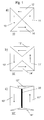
- spontaneously forms a domain structure which schematically in Fig. 1a ) with domains 11, 12, 13, 14 .
- the amounts of the magnetizations of the domains are the same size.
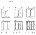
- Fig. 2 a) to c) the influence of the increasing length of a single slit 20, 20 ', 20 " on the magnetization in the ferromagnetic layer is shown, from which it can be seen that the volume fraction parallel to the longitudinal axis of each slit 20, 20', 20 " arranged and thus favorably oriented areas increasingly increased and thus at the same time the volume fraction of the perpendicular to the longitudinal axis of each slot 20, 20 ', 20' arranged and thus unfavorably oriented areas correspondingly reduced.
- the same effect is observed when, as in Fig. 2 d) to f) , at the same time the number of parallel slits of 20, 21 over 20 ', 21', 22 ' to 20'',21'',22'',23'' increases.
- FIG. 3 different geometries are shown schematically with slots arranged according to the invention.
- Fig. 3a shows a uniaxial arrangement with seven slits 20 to 26 oriented parallel to one another
- Fig. 3b a triangular arrangement with a tri-directional slot 30, each occupy an angle of approximately 120 ° to each other
- Fig. 3c an annular arrangement having a plurality of slots 20, 21 , etc. is shown, whose longitudinal axes are each arranged radially on the center 40 of a circle defined by the sides of the ring.
- Fig. 4 shows schematically an example of an arrangement of different slots according to the invention. Such an arrangement shows the adjustability of magnetic domains in arbitrary geometries.
Landscapes
- Engineering & Computer Science (AREA)
- Power Engineering (AREA)
- Manufacturing & Machinery (AREA)
- Thin Magnetic Films (AREA)
- Hall/Mr Elements (AREA)
Description
- Die Erfindung betrifft eine dünne ferro- oder ferrimagnetische Schicht, Verfahren zu ihrer Herstellung und ihre Verwendung.
- Passive oder aktive elektronische Bauelemente können ferro- oder ferrimagnetische Dünnschicht-Komponenten besitzen, die eine wesentliche Funktion des Bauelements bewirken. Zur Gewährleistung der Funktion dieser ferro- oder ferrimagnetischen Komponente ist es in vielen Fällen vorteilhaft, eine spezifische definierte magnetische Domänenstruktur bereitzustellen. Die sich in dünnen Schichten durch spontane Magnetisierung einstellende Domänenstruktur hängt in erster Linie von der Minimierung des Streufeldes ab. Daher ist in vielen Fällen, insbesondere dann, wenn die Materialeigenschaften über die Schicht nicht konstant sind, die Domänenstruktur nicht einstellbar.
- Die Einstellbarkeit der Domänenstruktur sowie ihre räumliche und zeitliche Stabilisierung ist andererseits eine grundlegende Voraussetzung für magnetoelektronische oder spintronische Bauelemente insbesondere im Bereich der Hochfrequenztechnik, der Sensorik, der Speichermedien und der Elektronik.
- Aus der
EP 1 168 383 A1 und derUS 6,529,110 B2 ist bekannt, magnetische Mikrostrukturen in einzelne Bereiche aufzuteilen. Hierzu wird ein magnetischer, sich innerhalb einer Spule befindlicher länglicher magnetischer Dünnschichtkern in mehrere quadratische oder rechteckige Bereiche aufgeteilt, wobei die Aufteilung des Dünnschichtkerns senkrecht zur Spulenachse erfolgt. Nachteilig hieran ist, dass eine vollständig getrennte Strukturierung zu relativ instabilen Domänenstrukturen führt, deren Ausbildung von der äußeren Geometrie abhängig ist und nicht direkt eingestellt werden kann. - K. FUJIMOTO ET AL. IEEE TRANSACTIONS ON MAGNETICS, Bd. 28, Nr. 6, (1992), Seiten 3350-3354 und D. KLEIN ET AL., JOURNAL OF APPLIED PHYSICS, Bd. 57, Nr. 1,(1985), Seiten 4071-4072 zeigen Domäneneinschluss in Schichten mit senkrechte Magnetisierung mittels Ätzen von Nuten in dieser Schichten.
- Ausgehend davon ist es die Aufgabe der Erfindung, eine ferro- oder ferrimagnetische Schicht, Verfahren zu ihrer Herstellung und ihre Verwendung anzugeben, die die vorher genannten Nachteile und Einschränkungen nicht aufweisen. Insbesondere soll eine ferro- oder ferrimagnetische Schicht angegeben werden, in der die Domänenstruktur weitgehend einstellbar ist.
- Gelöst wird die Aufgabe durch die Merkmale des Patentanspruchs 1, durch das Verfahren des Patentanspruchs 7 und durch die Verwendungen des Patentanspruchs 10. Die Unteransprüche beschreiben jeweils vorteilhafte Ausgestaltungen der Erfindung.
- Die der Erfindung zu Grunde liegende Idee besteht darin, durch einen oder mehrere längliche Schlitze, die in eine ferro- oder ferrimagnetische Dünnschicht eingebracht sind, einen Einfluss auf die Einstellung der Domänenstruktur auszuüben. Diese einstellbare Domänenstruktur ist der Schlüssel für die magnetisierungsabhängige Funktion eines Bauelements, das eine erfindungsgemäße Schicht umfasst. Eine derart mit Schlitzen versehene Schicht ermöglicht aufgrund der weitgehenden Verhinderung von Domänenwandbewegungen einen linearen Verlauf der Magnetisierung.
- Domänen, die eine Magnetisierungsrichtung aufweisen, die ungleich der erforderlichen Richtung liegen, sowie Domänenwände stellen Bereiche großer Verluste z.B. durch Wanderungsbewegungen im elektrischen Wechselfeld dar. Eine Schicht ohne Schlitze bildet eine Domänenstruktur mit ausgedehnten Domänenwänden und großen Domänenbereichen mit ineffektiv liegender Magnetisierungsrichtung aus. Durch erfindungsgemäße Schlitze wird der Bereich der ausgerichteten Magnetisierung signifikant vergrößert und das Domänenwandvolumen verringert sowie die Domänenwandbewegung reduziert. Die gezielte Ausrichtung der Magnetisierung von Domänen wird so ermöglicht.
- Eine erfindungsgemäße Schicht aus einem ferro- oder ferrimagnetischen Material ist direkt auf ein Substrat oder über eine oder mehrere zusätzliche elektrisch isolierende, halbleitende oder leitende nicht ferro- oder ferrimagnetische oder andere ferro- oder ferrimagnetische Zwischenschichten auf ein Substrat aufgebracht. Die Dicke der Schicht liegt bevorzugt zwischen 10 nm und 10 µm.
- Eine erfindungsgemäße Schicht umfasst weiterhin einen oder mehrere Schlitze, die länglich ausgebildet sind und daher eine definierte Längsachse aufweisen. Die Tiefe des Schlitzes bzw. der Schlitze entspricht der jeweiligen Dicke der Schicht und ihre Breite ist jeweils größer als die Austauschlänge des ferro- oder ferrimagnetischen Materials, die üblicherweise im Bereich zwischen 10 nm bis 100 nm liegt. Kein Schlitz ist so angebracht, dass er eine Seite (Rand) der Schicht berührt und damit die Schicht ggf. in mehrere Teile zerteilen würde. Vorzugsweise werden keine strom- oder spannungsführenden Leiterbahnen durch den Schlitz geführt.
- Die Schlitze besitzen vorzugsweise eine Länge, die der Geometrie der Schicht wie z.B. bei Rechtecken, Quadraten, Bändern, Dreiecken oder Ringen angepasst ist. In einer bevorzugten Ausgestaltung spannen die Seiten der Schicht ein Rechteck auf und die Längsachse des mindestens einen Schlitzes liegt im Wesentlichen parallel zu zwei gegenüberliegenden Seiten des Rechtecks. Die Länge jedes Schlitzes beträgt in diesem Falle bevorzugt zwischen dem 0,1- und dem 0,85-fachen, besonders bevorzugt zwischen dem 0,2- und dem 0,75-fachen einer Seite der Schicht, die im Wesentlichen parallel zur Längsachse des betreffenden Schlitzes verläuft.
- Der Abstand zweier benachbarter Schlitze in einer vorgegebenen Geometrie ist abhängig von Material und Dicke der Schicht und besitzt eine Grenze nach oben durch die Ausbildung von zusätzlichen Domänen zwischen diesen beiden Schlitzen und nach unten durch die Vergrößerung des durch zusätzliche Schlitze eingenommenen inaktiven Volumens. Vorzugsweise wird demnach ein Abstand gewählt, der als Optimum zwischen der Verringerung der Quermagnetisierung durch mehr Schlitze bei gleichzeitigem Verlust an Oberfläche auf der Schicht durch mehr Schlitze gegeben ist.
- Die Herstellung einer erfindungsgemäßen ferro- oder ferrimagnetischen Schicht erfolgt mittels eines Dünnschichtverfahrens.
Die so aufgebrachte Schicht wird durch Mikrostrukturtechniken in Bereiche strukturiert und es werden hiermit ein oder mehrere Schlitze eingebracht. Hierfür kommen gängige Verfahren wie z.B. Ionenstrahlätzen, Plasmastrahlätzen, reaktives Ionenätzen, nasschemisches Ätzen oder mechanischer Abtrag in Frage. Die so erzeugten Strukturen können eine beliebige, insbesondere eine quadratische, rechteckige, runde, elliptische oder ringförmige Geometrie aufweisen. - Die gewünschte Domänenstruktur stellt sich bei Verwendung geeigneter Schlitzgeometrien entweder spontan, also ohne zusätzliche Wärmebehandlung ein. In einer besonderen Ausgestaltung wird eine induzierte Anisotropie durch eine anschließende Wärmebehandlung der Schicht mit oder ohne externes Magnetfeld verstärkt eingeprägt. Im Allgemeinen kann jedoch in erfindungsgemäß geschlitzten Bereichen der Schicht auf die Wärmebehandlung der Schicht sowie auf das externe Magnetfeld während der Wärmebehandlung zum Einprägen einer uniaxialen Anisotropie verzichtet werden.
- Die vorliegende Erfindung ermöglicht damit die gezielte Einstellung von magnetischen Domänen in ferro- oder ferrimagnetischen Schichten mit beliebigen äußeren Geometrien, wobei ein hoher Anteil an gezielt ausgerichteten Bereichen innerhalb der Schicht erzeugt wird. Auch die Ausrichtung der Domänen in beliebigen geometrischen Dünnschichtstrukturen ist möglich. Damit wird eine gezielte Einstellbarkeit der Permeabilität und des Magnetisierungsverhaltens von magnetischen Schichtstrukturen über die Domänenstruktur möglich.
- Erfindungsgemäße Schichten eigenen sich für die Verwendung in magnetoelektronischen und spintronischen Bauelementen, insbesondere für die Bereiche Hochfrequenztechnik, Sensorik, Speichermedien und Elektronik.
- Die Erfindung wird im Folgenden an Hand von Ausführungsbeispielen mit Hilfe der Abbildungen näher erläutert. Es zeigen:
- Fig. 1
- Schematische Darstellung der Magnetisierung einer ferro- oder ferrimagnetischen Schicht
- a) nach spontaner Magnetisierung
- b) und anschließender Wärmebehandlung im externen Magnetfeld jeweils ohne erfindungsgemäßen Schlitz;
- c) nach spontaner Magnetisierung mit erfindungsgemäßen Schlitz.
- Fig. 2
-
- a)-c) Schematische Darstellung des Einflusses der Länge eines Schlitzes auf die Magnetisierung in der Schicht;
- d)-f) Schematische Darstellung des Einflusses der Länge eines Schlitzes bei gleichzeitig Zunahme der Anzahl von Schlitzen auf die Magnetisierung in der Schicht.
- Fig. 3
- Schematische Darstellung verschiedener Geometrien der Anordnung von erfindungsgemäßen Schlitzen:
- a) uniaxiale Anordnung;
- b) triangulare Anordnung,
- c) ringförmige Anordnung.
- Fig. 4
- Schematische Darstellung des Beispiels einer Anordnung von verschiedenen erfindungsgemäßen Schlitzen.
- Mittels reaktivem Magnetronsputtern wird eine ebene dünne Schicht 10 aus dem ferromagnetische Material FeCoTaN auf ein Substrat mit quadratischen lateralen Abmessungen von 20 µm x 20 µm aufgebracht. Die Dicke der Schicht 10 beträgt 100 nm und ist damit 200-fach geringer als die Kantenlänge. In einer derartigen Schicht 10 bildet sich spontan eine Domänenstruktur aus, die schematisch in
Fig. 1a ) mit den Domänen 11, 12, 13, 14 dargestellt ist. Dabei sind die Beträge der Magnetisierungen der Domänen gleich groß. - Es ist erforderlich, dass die Richtung der Magnetisierung in der Schicht vorliegt. Im Falle von uniaxialer Anisotropie sollen sich in jeweils benachbarten Bereichen der Schicht zwei entgegen gesetzte Richtungen der Magnetisierung ausbilden, während der Anteil der hierzu senkrecht stehenden Magnetisierungen möglichst gering sein soll. Diese Anforderungen lassen sich erfüllen, indem der Volumenanteil der günstig orientierten Bereiche 11, 13 vergrößert und damit gleichzeitig der Volumenanteil der hierzu senkrecht stehenden und damit ungünstig orientierten Bereiche 12, 14 entsprechend verringert wird.
- Durch eine aus dem Stand der Technik bekannte Wärmebehandlung der Schicht 10' in einem externen Magnetfeld ergibt sich, wie in
Fig. 1b ) dargestellt, nach dem Abschalten des externen Feldes eine Vergrößerung der Domänen 11, 13 zu den Domänen 11', 13' bis zu einem gewissen Maß. Eine weitere Vergrößerung der Domänen 11', 13' ist mit bekannten Maßnahmen nicht möglich. - Ist in der ferromagnetischen Schicht 10" jedoch ein Schlitz 20 eingebracht, dessen Ausrichtung parallel zur Orientierung der Magnetisierung in den Domänen 11, 13 verläuft, lassen sich, wie aus
Fig. 1c ) hervorgeht, die Domänen 11, 13 über das aus dem Stand der Technik bekannte Maß hinaus zu den Domänen 11", 13" vergrößern. Hierdurch ist der Volumenanteil der Domänen 11", 13" mit der gewünschten Richtung der Magnetisierung im Vergleich zu den Domänen 11, 13 signifikant höher, während der Volumenanteil der hierzu senkrecht stehenden und damit ungünstig ausgerichteten Domänen 12, 14 im Vergleich mit den Domänen 12", 14" signifikant niedriger ist. - In
Fig. 2 a) bis c) ist der Einfluss der zunehmenden Länge jeweils eines einzelnen Schlitzes 20, 20', 20" auf die Magnetisierung in der ferromagnetischen Schicht dargestellt. Hieraus ist ersichtlich, dass sich der Volumenanteil der parallel zur Längsachse des jeweils einen Schlitzes 20, 20', 20" angeordneten und damit günstig orientierten Bereiche zunehmend vergrößert und sich damit gleichzeitig der Volumenanteil der senkrecht zur Längsachse des jeweils einen Schlitzes 20, 20', 20" angeordneten und damit ungünstig orientierten Bereiche entsprechend verringert. Derselbe Effekt wird beobachtet, wenn, wie inFig. 2 d) bis f) dargestellt, gleichzeitig die Anzahl der jeweils parallel zueinander orientierten Schlitze von 20, 21 über 20', 21', 22' zu 20'', 21'', 22'', 23'' zunimmt. - In
Fig. 3 sind verschiedene Geometrien mit erfindungsgemäß angeordneten Schlitzen schematisch dargestellt.Fig. 3a ) zeigt eine uniaxiale Anordnung mit sieben parallel zueinander orientierten Schlitzen 20 bis 26,Fig. 3b ) eine triangulare Anordnung mit einem in drei Richtungen gefächerten Schlitz 30, die jeweils einen Winkel von ca. 120° zueinander einnehmen, während inFig. 3c ) eine ringförmige Anordnung mit einer Vielzahl von Schlitzen 20, 21 usw. dargestellt ist, deren Längsachsen jeweils radial auf den Mittelpunkt 40 eines durch die Seiten des Ringes definierten Kreises angeordnet sind. -
Fig. 4 zeigt schematisch ein Beispiel einer Anordnung von verschiedenen erfindungsgemäßen Schlitzen. Eine derartige Anordnung zeigt die Einstellbarkeit von magnetischen Domänen in beliebigen Geometrien.
Claims (10)
- Schicht aus einem ferro- oder ferrimagnetischen Material, die auf einem Substrat aufgebracht ist, wobei sie mindestens einen länglichen Schlitz zur Einstellung der Domänenstruktur im ferro- oder ferrimagnetischen Material umfasst,- dessen Tiefe der Dicke der Schicht entspricht,- dessen Breite größer als die Austauschlänge des Materials ist und- der so angebracht ist, dass er keine Seite der Schicht berührt,wobei die bevorzugte Richtung der Magnetisierung in der Schicht liegt.
- Schicht nach Anspruch 1, wobei keine strom- oder spannungsführenden Leiterbahnen durch den mindestens einen Schlitz geführt werden.
- Schicht nach Anspruch 2, wobei die Seiten der Schicht ein Rechteck aufspannen und die Längsachse des mindestens einen Schlitzes parallel zu zwei Seiten des Rechtecks liegt.
- Schicht nach Anspruch 3, wobei die Länge des mindestens einen Schlitzes zwischen dem 0,1- und dem 0,85-fachen der Länge einer Seite der Schicht beträgt, die parallel zur Längsachse des Schlitzes liegt.
- Schicht nach einem der Ansprüche 1 bis 4, wobei ihre Dicke zwischen 10 nm und 10 µm beträgt.
- Schicht nach einem der Ansprüche 1 bis 5, wobei sich zwischen der Schicht und dem Substrat mindestens eine weitere Schicht befindet.
- Verfahren zur Herstellung einer Schicht nach einem der Ansprüche 1 bis 6 mittels eines Dünnschichtverfahrens und Einbringen des mindestens einen Schlitzes mittels Ionenstrahlätzen, Plasmastrahlätzen, reaktivem Ionenätzen, nasschemischem Ätzen oder mechanischem Abtrag.
- Verfahren nach Anspruch 7 mit zusätzlicher Wärmebehandlung.
- Verfahren nach Anspruch 7 oder 8 unter zusätzlicher Einwirkung eines externen Magnetfelds.
- Verwendung einer Schicht nach einem der Ansprüche 1 bis 6 in magnetoelektronischen oder spintronischen Bauelementen.
Applications Claiming Priority (2)
| Application Number | Priority Date | Filing Date | Title |
|---|---|---|---|
| DE102005015745A DE102005015745A1 (de) | 2005-04-06 | 2005-04-06 | Ferro- oder ferrimagnetische Schicht, Verfahren zu ihrer Herstellung und ihre Verwendung |
| PCT/EP2006/002756 WO2006105877A1 (de) | 2005-04-06 | 2006-03-25 | Ferro- oder ferrimagnetische schicht, verfahren zu ihrer herstellung und ihre verwendung |
Publications (2)
| Publication Number | Publication Date |
|---|---|
| EP1866940A1 EP1866940A1 (de) | 2007-12-19 |
| EP1866940B1 true EP1866940B1 (de) | 2016-08-03 |
Family
ID=36589196
Family Applications (1)
| Application Number | Title | Priority Date | Filing Date |
|---|---|---|---|
| EP06723734.7A Expired - Lifetime EP1866940B1 (de) | 2005-04-06 | 2006-03-25 | Ferro- oder ferrimagnetische schicht, verfahren zu ihrer herstellung und ihre verwendung |
Country Status (6)
| Country | Link |
|---|---|
| US (1) | US7642098B2 (de) |
| EP (1) | EP1866940B1 (de) |
| JP (1) | JP5289938B2 (de) |
| KR (1) | KR20070117619A (de) |
| DE (1) | DE102005015745A1 (de) |
| WO (1) | WO2006105877A1 (de) |
Family Cites Families (14)
| Publication number | Priority date | Publication date | Assignee | Title |
|---|---|---|---|---|
| DE2701558A1 (de) * | 1977-01-15 | 1978-07-20 | Vogt Gmbh & Co Kg | Ringkern aus ferrit fuer drosselspulen mit nichtlinearem verlauf der permeabilitaet |
| JP3109839B2 (ja) * | 1990-12-21 | 2000-11-20 | 日本電信電話株式会社 | 高周波用薄膜トランス |
| JPH05234759A (ja) * | 1992-02-24 | 1993-09-10 | Tokin Corp | 薄膜インダクタ及びその製造方法 |
| JP3392444B2 (ja) * | 1992-09-30 | 2003-03-31 | 株式会社東芝 | 磁性人工格子膜 |
| JP3290828B2 (ja) * | 1994-09-16 | 2002-06-10 | 株式会社東芝 | 薄膜インダクタンス素子およびその製造方法 |
| FR2773632B1 (fr) | 1998-01-12 | 2000-03-31 | Centre Nat Rech Scient | Procede de gravure magnetique, pour notamment l'enregistrement magnetique ou magneto-optique |
| JP2000114047A (ja) * | 1998-10-07 | 2000-04-21 | Alps Electric Co Ltd | 薄膜トランス及び薄膜トランスの製造方法 |
| JP3230514B2 (ja) * | 1999-03-19 | 2001-11-19 | 日本電気株式会社 | 磁性配線 |
| US7724558B1 (en) * | 1999-03-19 | 2010-05-25 | Nec Corporation | Magnetic signal transmission line |
| FR2811135B1 (fr) * | 2000-06-29 | 2002-11-22 | Memscap | Microcomposant du type micro-inductance ou microtransformateur |
| DE10062400C2 (de) * | 2000-12-14 | 2003-07-24 | Daimler Chrysler Ag | Flexible Induktive Bauelemente für Leiterfolien |
| DE10102367B4 (de) * | 2001-01-19 | 2004-04-15 | Siemens Ag | Datenübertragungseinrichtung zur galvanisch getrennten Signalübertragung und Verwendung der Einrichtung |
| JP2003347124A (ja) * | 2002-05-27 | 2003-12-05 | Matsushita Electric Ind Co Ltd | 磁性素子およびこれを用いた電源モジュール |
| JP4431302B2 (ja) * | 2002-06-05 | 2010-03-10 | 財団法人電気磁気材料研究所 | 磁区制御された軟磁性薄膜フィルムおよびその製造方法ならびに高周波磁気デバイス |
-
2005
- 2005-04-06 DE DE102005015745A patent/DE102005015745A1/de not_active Ceased
-
2006
- 2006-03-25 KR KR1020077022393A patent/KR20070117619A/ko not_active Withdrawn
- 2006-03-25 WO PCT/EP2006/002756 patent/WO2006105877A1/de not_active Ceased
- 2006-03-25 US US11/910,633 patent/US7642098B2/en not_active Expired - Fee Related
- 2006-03-25 JP JP2008504648A patent/JP5289938B2/ja not_active Expired - Fee Related
- 2006-03-25 EP EP06723734.7A patent/EP1866940B1/de not_active Expired - Lifetime
Also Published As
| Publication number | Publication date |
|---|---|
| KR20070117619A (ko) | 2007-12-12 |
| JP5289938B2 (ja) | 2013-09-11 |
| EP1866940A1 (de) | 2007-12-19 |
| US7642098B2 (en) | 2010-01-05 |
| DE102005015745A1 (de) | 2006-10-12 |
| JP2008537329A (ja) | 2008-09-11 |
| WO2006105877A1 (de) | 2006-10-12 |
| US20080160333A1 (en) | 2008-07-03 |
Similar Documents
| Publication | Publication Date | Title |
|---|---|---|
| DE69830987T2 (de) | Elektronisches bauelement | |
| DE102017130379A1 (de) | Sensoreinrichtung mit kapazitivem Sensor für Kraftfahrzeuge | |
| WO2008101989A1 (de) | Halbleiterbauelement und verfahren zu dessen herstellung | |
| DE3032708C2 (de) | Verfahren zur Herstellung eines Dünnschicht-Magnetfeld-Sensors | |
| DE10157678C2 (de) | Hochfrequenzfestes Folienkabel für Datenleitungen | |
| DE3142949A1 (de) | Josephson-element und verfahren zu seiner herstellung | |
| EP2297797B1 (de) | Piezoelektrisches bauelement und verfahren zur herstellung eines elektrischen kontaktes | |
| EP3791408B1 (de) | Verfahren zum herstellen einer atomfalle sowie atomfalle | |
| WO2003023795A1 (de) | Magnetisches bauelement | |
| DE69807571T2 (de) | Verfahren und Vorrichtung zum Ätzen | |
| WO2006105877A1 (de) | Ferro- oder ferrimagnetische schicht, verfahren zu ihrer herstellung und ihre verwendung | |
| DE1424518A1 (de) | Speicheranordnung | |
| DE112020006358T5 (de) | Magnetsensor und verfahren zur herstellung eines magnetsensors | |
| DE2539795C3 (de) | Generator zur Erzeugung magnetischer Blasendomänen | |
| WO2014108499A1 (de) | Verfahren und vorrichtung zum herstellen eines multilagenelektrodensystems | |
| DE112020006325T5 (de) | Magnetsensor | |
| EP1882269B1 (de) | Vorrichtung zur Dämpfung von Reflexionen elektromagnetischer Wellen, Verfahren zur Herstellung und ihre Verwendung | |
| EP2686865B1 (de) | Phasenkontrasteinheit und herstellungsverfahren dafür | |
| EP1298757A1 (de) | Bandpassfilter für ein Hochfrequenzsignal und Abstimmverfahren dafür | |
| DE1789148C (de) | Induktives Halbleiter-Bauelement, Verfahren zum Herstellen und Verwendung | |
| EP0793861B1 (de) | Tunnel-effekt bauelement und verfahren zu seiner herstellung | |
| DE102023116486A1 (de) | Magnetsensor, verfahren zur herstellung eines magnetsensors und sensitivelementanordnung | |
| DE102017111464B4 (de) | Kompakte kondensatoren und verfahren zu ihrer herstellung | |
| EP4672610A1 (de) | Spulenanordnung auf einer multilayer-platine und verfahren zum herstellen einer spulenanordnung | |
| EP1704606A1 (de) | Organischer transistor mit selbstjustierender gate-elektrode und verfahren zu dessen herstellung |
Legal Events
| Date | Code | Title | Description |
|---|---|---|---|
| PUAI | Public reference made under article 153(3) epc to a published international application that has entered the european phase |
Free format text: ORIGINAL CODE: 0009012 |
|
| 17P | Request for examination filed |
Effective date: 20070616 |
|
| AK | Designated contracting states |
Kind code of ref document: A1 Designated state(s): AT BE BG CH CY CZ DE DK EE ES FI FR GB GR HU IE IS IT LI LT LU LV MC NL PL PT RO SE SI SK TR |
|
| DAX | Request for extension of the european patent (deleted) | ||
| 17Q | First examination report despatched |
Effective date: 20090127 |
|
| RAP1 | Party data changed (applicant data changed or rights of an application transferred) |
Owner name: KARLSRUHER INSTITUT FUER TECHNOLOGIE |
|
| GRAP | Despatch of communication of intention to grant a patent |
Free format text: ORIGINAL CODE: EPIDOSNIGR1 |
|
| INTG | Intention to grant announced |
Effective date: 20160118 |
|
| GRAS | Grant fee paid |
Free format text: ORIGINAL CODE: EPIDOSNIGR3 |
|
| GRAA | (expected) grant |
Free format text: ORIGINAL CODE: 0009210 |
|
| AK | Designated contracting states |
Kind code of ref document: B1 Designated state(s): AT BE BG CH CY CZ DE DK EE ES FI FR GB GR HU IE IS IT LI LT LU LV MC NL PL PT RO SE SI SK TR |
|
| REG | Reference to a national code |
Ref country code: GB Ref legal event code: FG4D Free format text: NOT ENGLISH |
|
| REG | Reference to a national code |
Ref country code: CH Ref legal event code: EP Ref country code: AT Ref legal event code: REF Ref document number: 817822 Country of ref document: AT Kind code of ref document: T Effective date: 20160815 |
|
| REG | Reference to a national code |
Ref country code: IE Ref legal event code: FG4D Free format text: LANGUAGE OF EP DOCUMENT: GERMAN |
|
| REG | Reference to a national code |
Ref country code: DE Ref legal event code: R096 Ref document number: 502006015078 Country of ref document: DE |
|
| REG | Reference to a national code |
Ref country code: NL Ref legal event code: MP Effective date: 20160803 |
|
| REG | Reference to a national code |
Ref country code: LT Ref legal event code: MG4D |
|
| PG25 | Lapsed in a contracting state [announced via postgrant information from national office to epo] |
Ref country code: LT Free format text: LAPSE BECAUSE OF FAILURE TO SUBMIT A TRANSLATION OF THE DESCRIPTION OR TO PAY THE FEE WITHIN THE PRESCRIBED TIME-LIMIT Effective date: 20160803 Ref country code: NL Free format text: LAPSE BECAUSE OF FAILURE TO SUBMIT A TRANSLATION OF THE DESCRIPTION OR TO PAY THE FEE WITHIN THE PRESCRIBED TIME-LIMIT Effective date: 20160803 Ref country code: FI Free format text: LAPSE BECAUSE OF FAILURE TO SUBMIT A TRANSLATION OF THE DESCRIPTION OR TO PAY THE FEE WITHIN THE PRESCRIBED TIME-LIMIT Effective date: 20160803 Ref country code: IS Free format text: LAPSE BECAUSE OF FAILURE TO SUBMIT A TRANSLATION OF THE DESCRIPTION OR TO PAY THE FEE WITHIN THE PRESCRIBED TIME-LIMIT Effective date: 20161203 |
|
| PG25 | Lapsed in a contracting state [announced via postgrant information from national office to epo] |
Ref country code: SE Free format text: LAPSE BECAUSE OF FAILURE TO SUBMIT A TRANSLATION OF THE DESCRIPTION OR TO PAY THE FEE WITHIN THE PRESCRIBED TIME-LIMIT Effective date: 20160803 Ref country code: LV Free format text: LAPSE BECAUSE OF FAILURE TO SUBMIT A TRANSLATION OF THE DESCRIPTION OR TO PAY THE FEE WITHIN THE PRESCRIBED TIME-LIMIT Effective date: 20160803 Ref country code: GR Free format text: LAPSE BECAUSE OF FAILURE TO SUBMIT A TRANSLATION OF THE DESCRIPTION OR TO PAY THE FEE WITHIN THE PRESCRIBED TIME-LIMIT Effective date: 20161104 Ref country code: PL Free format text: LAPSE BECAUSE OF FAILURE TO SUBMIT A TRANSLATION OF THE DESCRIPTION OR TO PAY THE FEE WITHIN THE PRESCRIBED TIME-LIMIT Effective date: 20160803 Ref country code: ES Free format text: LAPSE BECAUSE OF FAILURE TO SUBMIT A TRANSLATION OF THE DESCRIPTION OR TO PAY THE FEE WITHIN THE PRESCRIBED TIME-LIMIT Effective date: 20160803 Ref country code: PT Free format text: LAPSE BECAUSE OF FAILURE TO SUBMIT A TRANSLATION OF THE DESCRIPTION OR TO PAY THE FEE WITHIN THE PRESCRIBED TIME-LIMIT Effective date: 20161205 |
|
| REG | Reference to a national code |
Ref country code: FR Ref legal event code: PLFP Year of fee payment: 12 |
|
| PG25 | Lapsed in a contracting state [announced via postgrant information from national office to epo] |
Ref country code: EE Free format text: LAPSE BECAUSE OF FAILURE TO SUBMIT A TRANSLATION OF THE DESCRIPTION OR TO PAY THE FEE WITHIN THE PRESCRIBED TIME-LIMIT Effective date: 20160803 Ref country code: RO Free format text: LAPSE BECAUSE OF FAILURE TO SUBMIT A TRANSLATION OF THE DESCRIPTION OR TO PAY THE FEE WITHIN THE PRESCRIBED TIME-LIMIT Effective date: 20160803 |
|
| REG | Reference to a national code |
Ref country code: DE Ref legal event code: R097 Ref document number: 502006015078 Country of ref document: DE |
|
| PG25 | Lapsed in a contracting state [announced via postgrant information from national office to epo] |
Ref country code: SK Free format text: LAPSE BECAUSE OF FAILURE TO SUBMIT A TRANSLATION OF THE DESCRIPTION OR TO PAY THE FEE WITHIN THE PRESCRIBED TIME-LIMIT Effective date: 20160803 Ref country code: CZ Free format text: LAPSE BECAUSE OF FAILURE TO SUBMIT A TRANSLATION OF THE DESCRIPTION OR TO PAY THE FEE WITHIN THE PRESCRIBED TIME-LIMIT Effective date: 20160803 Ref country code: DK Free format text: LAPSE BECAUSE OF FAILURE TO SUBMIT A TRANSLATION OF THE DESCRIPTION OR TO PAY THE FEE WITHIN THE PRESCRIBED TIME-LIMIT Effective date: 20160803 Ref country code: BG Free format text: LAPSE BECAUSE OF FAILURE TO SUBMIT A TRANSLATION OF THE DESCRIPTION OR TO PAY THE FEE WITHIN THE PRESCRIBED TIME-LIMIT Effective date: 20161103 |
|
| PLBE | No opposition filed within time limit |
Free format text: ORIGINAL CODE: 0009261 |
|
| STAA | Information on the status of an ep patent application or granted ep patent |
Free format text: STATUS: NO OPPOSITION FILED WITHIN TIME LIMIT |
|
| 26N | No opposition filed |
Effective date: 20170504 |
|
| PG25 | Lapsed in a contracting state [announced via postgrant information from national office to epo] |
Ref country code: SI Free format text: LAPSE BECAUSE OF FAILURE TO SUBMIT A TRANSLATION OF THE DESCRIPTION OR TO PAY THE FEE WITHIN THE PRESCRIBED TIME-LIMIT Effective date: 20160803 |
|
| REG | Reference to a national code |
Ref country code: CH Ref legal event code: PL |
|
| PG25 | Lapsed in a contracting state [announced via postgrant information from national office to epo] |
Ref country code: MC Free format text: LAPSE BECAUSE OF FAILURE TO SUBMIT A TRANSLATION OF THE DESCRIPTION OR TO PAY THE FEE WITHIN THE PRESCRIBED TIME-LIMIT Effective date: 20160803 |
|
| REG | Reference to a national code |
Ref country code: IE Ref legal event code: MM4A |
|
| PG25 | Lapsed in a contracting state [announced via postgrant information from national office to epo] |
Ref country code: LU Free format text: LAPSE BECAUSE OF NON-PAYMENT OF DUE FEES Effective date: 20170325 |
|
| PG25 | Lapsed in a contracting state [announced via postgrant information from national office to epo] |
Ref country code: CH Free format text: LAPSE BECAUSE OF NON-PAYMENT OF DUE FEES Effective date: 20170331 Ref country code: LI Free format text: LAPSE BECAUSE OF NON-PAYMENT OF DUE FEES Effective date: 20170331 Ref country code: IE Free format text: LAPSE BECAUSE OF NON-PAYMENT OF DUE FEES Effective date: 20170325 |
|
| REG | Reference to a national code |
Ref country code: BE Ref legal event code: MM Effective date: 20170331 |
|
| REG | Reference to a national code |
Ref country code: FR Ref legal event code: PLFP Year of fee payment: 13 |
|
| PG25 | Lapsed in a contracting state [announced via postgrant information from national office to epo] |
Ref country code: BE Free format text: LAPSE BECAUSE OF NON-PAYMENT OF DUE FEES Effective date: 20170331 |
|
| PGFP | Annual fee paid to national office [announced via postgrant information from national office to epo] |
Ref country code: IT Payment date: 20190321 Year of fee payment: 14 Ref country code: GB Payment date: 20190325 Year of fee payment: 14 Ref country code: DE Payment date: 20190325 Year of fee payment: 14 Ref country code: FR Payment date: 20190326 Year of fee payment: 14 |
|
| PGFP | Annual fee paid to national office [announced via postgrant information from national office to epo] |
Ref country code: AT Payment date: 20190319 Year of fee payment: 14 |
|
| PG25 | Lapsed in a contracting state [announced via postgrant information from national office to epo] |
Ref country code: HU Free format text: LAPSE BECAUSE OF FAILURE TO SUBMIT A TRANSLATION OF THE DESCRIPTION OR TO PAY THE FEE WITHIN THE PRESCRIBED TIME-LIMIT; INVALID AB INITIO Effective date: 20060325 |
|
| PG25 | Lapsed in a contracting state [announced via postgrant information from national office to epo] |
Ref country code: CY Free format text: LAPSE BECAUSE OF NON-PAYMENT OF DUE FEES Effective date: 20160803 |
|
| PG25 | Lapsed in a contracting state [announced via postgrant information from national office to epo] |
Ref country code: TR Free format text: LAPSE BECAUSE OF FAILURE TO SUBMIT A TRANSLATION OF THE DESCRIPTION OR TO PAY THE FEE WITHIN THE PRESCRIBED TIME-LIMIT Effective date: 20160803 |
|
| REG | Reference to a national code |
Ref country code: DE Ref legal event code: R119 Ref document number: 502006015078 Country of ref document: DE |
|
| REG | Reference to a national code |
Ref country code: AT Ref legal event code: MM01 Ref document number: 817822 Country of ref document: AT Kind code of ref document: T Effective date: 20200325 |
|
| PG25 | Lapsed in a contracting state [announced via postgrant information from national office to epo] |
Ref country code: AT Free format text: LAPSE BECAUSE OF NON-PAYMENT OF DUE FEES Effective date: 20200325 Ref country code: DE Free format text: LAPSE BECAUSE OF NON-PAYMENT OF DUE FEES Effective date: 20201001 Ref country code: FR Free format text: LAPSE BECAUSE OF NON-PAYMENT OF DUE FEES Effective date: 20200331 |
|
| GBPC | Gb: european patent ceased through non-payment of renewal fee |
Effective date: 20200325 |
|
| PG25 | Lapsed in a contracting state [announced via postgrant information from national office to epo] |
Ref country code: GB Free format text: LAPSE BECAUSE OF NON-PAYMENT OF DUE FEES Effective date: 20200325 |
|
| PG25 | Lapsed in a contracting state [announced via postgrant information from national office to epo] |
Ref country code: IT Free format text: LAPSE BECAUSE OF NON-PAYMENT OF DUE FEES Effective date: 20200325 |