EP1857522B1 - Multiprimary color display - Google Patents
Multiprimary color display Download PDFInfo
- Publication number
- EP1857522B1 EP1857522B1 EP07107451A EP07107451A EP1857522B1 EP 1857522 B1 EP1857522 B1 EP 1857522B1 EP 07107451 A EP07107451 A EP 07107451A EP 07107451 A EP07107451 A EP 07107451A EP 1857522 B1 EP1857522 B1 EP 1857522B1
- Authority
- EP
- European Patent Office
- Prior art keywords
- green
- light emission
- yellow
- display
- chromaticity coordinates
- Prior art date
- Legal status (The legal status is an assumption and is not a legal conclusion. Google has not performed a legal analysis and makes no representation as to the accuracy of the status listed.)
- Not-in-force
Links
- 239000003086 colorant Substances 0.000 claims description 29
- 229910014780 CaAl2 Inorganic materials 0.000 claims description 9
- 238000010894 electron beam technology Methods 0.000 claims description 9
- 108010043121 Green Fluorescent Proteins Proteins 0.000 claims description 2
- 239000010408 film Substances 0.000 description 21
- 239000000463 material Substances 0.000 description 15
- 238000010586 diagram Methods 0.000 description 12
- 238000000034 method Methods 0.000 description 11
- 239000000758 substrate Substances 0.000 description 10
- 239000011159 matrix material Substances 0.000 description 9
- 230000000052 comparative effect Effects 0.000 description 7
- 238000000295 emission spectrum Methods 0.000 description 7
- 238000004544 sputter deposition Methods 0.000 description 7
- 239000010409 thin film Substances 0.000 description 7
- 239000004973 liquid crystal related substance Substances 0.000 description 6
- 238000004519 manufacturing process Methods 0.000 description 5
- 239000011521 glass Substances 0.000 description 4
- 238000004737 colorimetric analysis Methods 0.000 description 3
- 230000003247 decreasing effect Effects 0.000 description 3
- 230000006866 deterioration Effects 0.000 description 3
- 239000000843 powder Substances 0.000 description 3
- XKRFYHLGVUSROY-UHFFFAOYSA-N Argon Chemical compound [Ar] XKRFYHLGVUSROY-UHFFFAOYSA-N 0.000 description 2
- 239000005132 Calcium sulfide based phosphorescent agent Substances 0.000 description 2
- ZOKXTWBITQBERF-UHFFFAOYSA-N Molybdenum Chemical compound [Mo] ZOKXTWBITQBERF-UHFFFAOYSA-N 0.000 description 2
- VYPSYNLAJGMNEJ-UHFFFAOYSA-N Silicium dioxide Chemical compound O=[Si]=O VYPSYNLAJGMNEJ-UHFFFAOYSA-N 0.000 description 2
- 229910052782 aluminium Inorganic materials 0.000 description 2
- XAGFODPZIPBFFR-UHFFFAOYSA-N aluminium Chemical compound [Al] XAGFODPZIPBFFR-UHFFFAOYSA-N 0.000 description 2
- 238000005229 chemical vapour deposition Methods 0.000 description 2
- 238000000151 deposition Methods 0.000 description 2
- 235000021384 green leafy vegetables Nutrition 0.000 description 2
- 230000006698 induction Effects 0.000 description 2
- 239000000976 ink Substances 0.000 description 2
- 229910052750 molybdenum Inorganic materials 0.000 description 2
- 239000011733 molybdenum Substances 0.000 description 2
- 238000007650 screen-printing Methods 0.000 description 2
- PBCFLUZVCVVTBY-UHFFFAOYSA-N tantalum pentoxide Inorganic materials O=[Ta](=O)O[Ta](=O)=O PBCFLUZVCVVTBY-UHFFFAOYSA-N 0.000 description 2
- 229910000980 Aluminium gallium arsenide Inorganic materials 0.000 description 1
- 229910016064 BaSi2 Inorganic materials 0.000 description 1
- RWSOTUBLDIXVET-UHFFFAOYSA-N Dihydrogen sulfide Chemical compound S RWSOTUBLDIXVET-UHFFFAOYSA-N 0.000 description 1
- 229910052693 Europium Inorganic materials 0.000 description 1
- 229910003564 SiAlON Inorganic materials 0.000 description 1
- RTAQQCXQSZGOHL-UHFFFAOYSA-N Titanium Chemical compound [Ti] RTAQQCXQSZGOHL-UHFFFAOYSA-N 0.000 description 1
- 229910052786 argon Inorganic materials 0.000 description 1
- 239000011230 binding agent Substances 0.000 description 1
- 238000002425 crystallisation Methods 0.000 description 1
- 230000008025 crystallization Effects 0.000 description 1
- 230000001419 dependent effect Effects 0.000 description 1
- 230000008021 deposition Effects 0.000 description 1
- 230000002542 deteriorative effect Effects 0.000 description 1
- 238000011161 development Methods 0.000 description 1
- 230000018109 developmental process Effects 0.000 description 1
- 229910052637 diopside Inorganic materials 0.000 description 1
- 238000007599 discharging Methods 0.000 description 1
- 230000000694 effects Effects 0.000 description 1
- 238000005401 electroluminescence Methods 0.000 description 1
- 238000005516 engineering process Methods 0.000 description 1
- 238000005530 etching Methods 0.000 description 1
- 238000010438 heat treatment Methods 0.000 description 1
- 229910000037 hydrogen sulfide Inorganic materials 0.000 description 1
- AMGQUBHHOARCQH-UHFFFAOYSA-N indium;oxotin Chemical compound [In].[Sn]=O AMGQUBHHOARCQH-UHFFFAOYSA-N 0.000 description 1
- 239000007788 liquid Substances 0.000 description 1
- 229910052751 metal Inorganic materials 0.000 description 1
- 239000002184 metal Substances 0.000 description 1
- 238000002156 mixing Methods 0.000 description 1
- BPUBBGLMJRNUCC-UHFFFAOYSA-N oxygen(2-);tantalum(5+) Chemical compound [O-2].[O-2].[O-2].[O-2].[O-2].[Ta+5].[Ta+5] BPUBBGLMJRNUCC-UHFFFAOYSA-N 0.000 description 1
- 238000000206 photolithography Methods 0.000 description 1
- 238000007639 printing Methods 0.000 description 1
- 230000035945 sensitivity Effects 0.000 description 1
- 235000012239 silicon dioxide Nutrition 0.000 description 1
- 239000000377 silicon dioxide Substances 0.000 description 1
- 238000004611 spectroscopical analysis Methods 0.000 description 1
- 229910001936 tantalum oxide Inorganic materials 0.000 description 1
- 239000010936 titanium Substances 0.000 description 1
- 229910052719 titanium Inorganic materials 0.000 description 1
Images

Classifications
-
- H—ELECTRICITY
- H01—ELECTRIC ELEMENTS
- H01J—ELECTRIC DISCHARGE TUBES OR DISCHARGE LAMPS
- H01J9/00—Apparatus or processes specially adapted for the manufacture, installation, removal, maintenance of electric discharge tubes, discharge lamps, or parts thereof; Recovery of material from discharge tubes or lamps
- H01J9/20—Manufacture of screens on or from which an image or pattern is formed, picked up, converted or stored; Applying coatings to the vessel
- H01J9/22—Applying luminescent coatings
- H01J9/227—Applying luminescent coatings with luminescent material discontinuously arranged, e.g. in dots or lines
- H01J9/2278—Application of light absorbing material, e.g. between the luminescent areas
-
- H—ELECTRICITY
- H05—ELECTRIC TECHNIQUES NOT OTHERWISE PROVIDED FOR
- H05B—ELECTRIC HEATING; ELECTRIC LIGHT SOURCES NOT OTHERWISE PROVIDED FOR; CIRCUIT ARRANGEMENTS FOR ELECTRIC LIGHT SOURCES, IN GENERAL
- H05B33/00—Electroluminescent light sources
- H05B33/02—Details
-
- C—CHEMISTRY; METALLURGY
- C09—DYES; PAINTS; POLISHES; NATURAL RESINS; ADHESIVES; COMPOSITIONS NOT OTHERWISE PROVIDED FOR; APPLICATIONS OF MATERIALS NOT OTHERWISE PROVIDED FOR
- C09K—MATERIALS FOR MISCELLANEOUS APPLICATIONS, NOT PROVIDED FOR ELSEWHERE
- C09K11/00—Luminescent, e.g. electroluminescent, chemiluminescent materials
- C09K11/08—Luminescent, e.g. electroluminescent, chemiluminescent materials containing inorganic luminescent materials
- C09K11/58—Luminescent, e.g. electroluminescent, chemiluminescent materials containing inorganic luminescent materials containing copper, silver or gold
- C09K11/582—Chalcogenides
- C09K11/584—Chalcogenides with zinc or cadmium
-
- C—CHEMISTRY; METALLURGY
- C09—DYES; PAINTS; POLISHES; NATURAL RESINS; ADHESIVES; COMPOSITIONS NOT OTHERWISE PROVIDED FOR; APPLICATIONS OF MATERIALS NOT OTHERWISE PROVIDED FOR
- C09K—MATERIALS FOR MISCELLANEOUS APPLICATIONS, NOT PROVIDED FOR ELSEWHERE
- C09K11/00—Luminescent, e.g. electroluminescent, chemiluminescent materials
- C09K11/08—Luminescent, e.g. electroluminescent, chemiluminescent materials containing inorganic luminescent materials
- C09K11/77—Luminescent, e.g. electroluminescent, chemiluminescent materials containing inorganic luminescent materials containing rare earth metals
- C09K11/7728—Luminescent, e.g. electroluminescent, chemiluminescent materials containing inorganic luminescent materials containing rare earth metals containing europium
- C09K11/7729—Chalcogenides
- C09K11/7731—Chalcogenides with alkaline earth metals
-
- C—CHEMISTRY; METALLURGY
- C09—DYES; PAINTS; POLISHES; NATURAL RESINS; ADHESIVES; COMPOSITIONS NOT OTHERWISE PROVIDED FOR; APPLICATIONS OF MATERIALS NOT OTHERWISE PROVIDED FOR
- C09K—MATERIALS FOR MISCELLANEOUS APPLICATIONS, NOT PROVIDED FOR ELSEWHERE
- C09K11/00—Luminescent, e.g. electroluminescent, chemiluminescent materials
- C09K11/08—Luminescent, e.g. electroluminescent, chemiluminescent materials containing inorganic luminescent materials
- C09K11/77—Luminescent, e.g. electroluminescent, chemiluminescent materials containing inorganic luminescent materials containing rare earth metals
- C09K11/7783—Luminescent, e.g. electroluminescent, chemiluminescent materials containing inorganic luminescent materials containing rare earth metals containing two or more rare earth metals one of which being europium
- C09K11/7784—Chalcogenides
- C09K11/7787—Oxides
-
- H—ELECTRICITY
- H01—ELECTRIC ELEMENTS
- H01J—ELECTRIC DISCHARGE TUBES OR DISCHARGE LAMPS
- H01J11/00—Gas-filled discharge tubes with alternating current induction of the discharge, e.g. alternating current plasma display panels [AC-PDP]; Gas-filled discharge tubes without any main electrode inside the vessel; Gas-filled discharge tubes with at least one main electrode outside the vessel
- H01J11/10—AC-PDPs with at least one main electrode being out of contact with the plasma
-
- H—ELECTRICITY
- H01—ELECTRIC ELEMENTS
- H01J—ELECTRIC DISCHARGE TUBES OR DISCHARGE LAMPS
- H01J11/00—Gas-filled discharge tubes with alternating current induction of the discharge, e.g. alternating current plasma display panels [AC-PDP]; Gas-filled discharge tubes without any main electrode inside the vessel; Gas-filled discharge tubes with at least one main electrode outside the vessel
- H01J11/20—Constructional details
- H01J11/34—Vessels, containers or parts thereof, e.g. substrates
- H01J11/42—Fluorescent layers
-
- H—ELECTRICITY
- H01—ELECTRIC ELEMENTS
- H01J—ELECTRIC DISCHARGE TUBES OR DISCHARGE LAMPS
- H01J31/00—Cathode ray tubes; Electron beam tubes
- H01J31/08—Cathode ray tubes; Electron beam tubes having a screen on or from which an image or pattern is formed, picked up, converted, or stored
- H01J31/10—Image or pattern display tubes, i.e. having electrical input and optical output; Flying-spot tubes for scanning purposes
- H01J31/12—Image or pattern display tubes, i.e. having electrical input and optical output; Flying-spot tubes for scanning purposes with luminescent screen
- H01J31/123—Flat display tubes
- H01J31/125—Flat display tubes provided with control means permitting the electron beam to reach selected parts of the screen, e.g. digital selection
- H01J31/127—Flat display tubes provided with control means permitting the electron beam to reach selected parts of the screen, e.g. digital selection using large area or array sources, i.e. essentially a source for each pixel group
Definitions
- the present invention relates to a multiprimary color display.
- a conventional type image display device (simply called a display hereinafter) is being replaced with a flat panel display in the fields from personal computers to at-home TV receivers.
- the IEC International Electro-technical Commission
- sRGB which is the standard for a normal display. That is, by matching chromaticity points of three primary colors RGB with colorimetry parameters of Rec. 709 recommended by the ITU-R (International Telecommunication Union Radiocommunication sector), the relation between a video signal RGB and a colorimetry value was clearly defined. Therefore, if the same video signal RGB is given to a display according to the relevant normal display standard, the relevant display can colorimetrically display the same color.
- the display is widely used not only in case of displaying images for viewing but also in case of editing images. For example, the relevant display is used in case of creating an original to be printed as a catalog. Consequently, the normal display "sRGB display" which can be colorimetrically managed is the main point of color management including a hard copy system such as printing.
- each of Japanese Patent Application Laid-Open Nos. 2001-306023 and 2003-228360 discloses that sub pixels to which cyan, magenta and yellow inks, in addition to conventional red (R), green (G) and blue (B) inks, are emitted are provided.
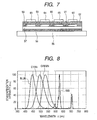
- Fig. 8 is a diagram illustrating a light emission spectrum of cyan, in addition to light emission spectra of conventional red (R), green (G) and blue (B).
- a peak of light emission is set to "100".
- each of Japanese Patent Application Laid-Open Nos. 2003-249174 and 2004-152737 discloses a technique for improving color reproducibility of a plasma display. More specifically, it is disclosed in each of these documents to improve color reproducibility by adding cyan-green in addition to conventional red (R), green (G) and blue (B). It should be noted that the conventional arts disclosed in these documents aim to further enlarge a color space because a color range defined by the sRGB is narrower than the color space perceivable by human eyes.
- Japanese Patent Application Laid-Open No. 2004-163817 discloses a technique for enlarging a color reproducible range on a projector to which second green has been added in addition to conventional three projector display colors.
- a color filter constituting a pixel 5 includes pixels of red (R) 7, green (G) 8 and blue (B) 9 respectively separated by a black matrix 6. That is, since color displaying is executed by the color filters of three colors, i.e. red (R) 7, green (G) 8 and blue (B) 9, expression of cyan is insufficient due to the characteristic of the color filter of green (G).
- Japanese Patent Application Laid-Open No. 2001-306023 discloses the technique for improving the expression of cyan due to the characteristic of the color filter. More specifically, in Japanese Patent Application Laid-Open No. 2001-306023 , the sub pixel (called "pixel” hereinafter) at least including cyan is provided to improve the color reproducibility.
- the colors which constitute the pixel include magenta and yellow in addition to cyan which are the three primary colors in a subtractive color mixing method.
- Japanese Patent Application Laid-Open No. 2003-228360 discloses the technique for improving a drawback in Japanese Patent Application Laid-Open No. 2001-306023 . That is, in Japanese Patent Application Laid-Open No. 2003-228360 , the luminance of cyan is made smaller than that of green (G) so as to achieve the "sRGB display".
- each of Japanese Patent Application Laid-Open Nos. 2003-249174 and 2004-152737 discloses that cyan-green is added to red (R), green (G) and blue (B).
- an area of one pixel is determined from an area of a display screen and the number of total pixels. Further, each pixel element constituting the pixel is surrounded with the black matrix. For this reason, if the number of pixel elements is increased from three to four, the area of each pixel element becomes equal to or less than 3/4 of the area of the pixel element of the three-pixel-element constitution.
- US patent application 2005/168127 A1 discloses a white light LED according to the preamble of claim 1, using a light source of at least four primary colors being red, green, blue, yellow light emitted by respective fluorescent powders.
- the present invention provides a display which can achieve a wide color reproduction range, high luminance and high-efficiency performance concurrently.
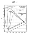
- Fig. 1 is a diagram illustrating a color reproduction range according to the present invention.
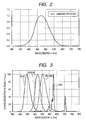
- Fig. 2 is a diagram illustrating a luminous efficiency curve.
- Fig. 3 is a diagram illustrating light emission spectra according to the present invention.
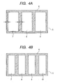
- Figs. 4A and 4B are diagrams respectively illustrating pixel shapes.
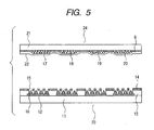
- Fig. 5 is a schematic diagram illustrating an FED (Field Emission Display) according to the present invention.
- Fig. 6 is a schematic cross section diagram illustrating the FED according to the present invention.
- Fig. 7 is a schematic cross section diagram illustrating an inorganic EL (electroluminescence) display according to the present invention.
- Fig. 8 is a diagram illustrating conventional light emission spectra.
- the NTSC (National Television System Committee) RGB representing a wider color reproduction range has been determined other than the sRGB as the chromaticity points of the RGB three primary colors. Further, it should be noted that the color reproduction range of the NTSC RGB is wider than the color reproduction range of the sRGB.
- red (0.670, 0.330), green (0.210, 0.710), blue (0.140, 0.080) and white (0.3101, 0.3162) have been determined as the CIE chromaticity coordinates.
- red (0.640, 0.330), green (0.300, 0.600), blue (0.150, 0.060) and white (0.3127, 0.3290) have been determined as the CIE chromaticity coordinates.
- the light mission efficiency has been determined based on the light emission intensity of white.
- the present invention aims to provide the flat panel display which can acquire a wider color reproduction range without sacrificing luminance.
- the present invention is characterized in that a light source (including a fluorescent member) of at least four or more colors is used, and at least one color of the light source is yellow.
- blue is at least the blue represented by the NTSC RGB CIE chromaticity coordinates and red is at least the red represented by the red CIE chromaticity coordinates.
- red is not limited to them respectively.
- the CIE chromaticity coordinates (x, y) of yellow are preferable to satisfy 0.24 ⁇ x ⁇ 0.45 and 0.56 ⁇ y ⁇ 0.76 outside a triangle of the CIE chromaticity coordinates (0.670, 0.330), (0.210, 0.710) and (0.140, 0.080) and within the visible range of the CIE chromaticity coordinates.
- the CIE chromaticity coordinates (x, y) of green are preferable to satisfy x ⁇ 0.210 within the visible range of the CIE chromaticity coordinates and to be larger than "y" of the CIE chromaticity coordinates of yellow.
- "y" of the CIE chromaticity coordinates (x, y) of green is preferable to satisfy y ⁇ 0.710.
- the CIE chromaticity coordinates (x, y) of green are further preferable to satisfy x ⁇ 0.210 and y ⁇ 0.710, within the visible range of the CIE chromaticity coordinates, on the side opposite to the color reproduction range of the NTSC RGB in regard to the line segment between the color coordinates (x, y) and the CIE chromaticity coordinates (0.210, 0.710) of yellow, because the color reproduction range in this case completely covers the color reproduction range of the NTSC RGB.
- the luminous efficacy of green is slightly deteriorated as compared with that of conventional green, it is possible to prevent deterioration of luminance by adding yellow of which the luminous efficacy is higher than that of conventional green.
- the display to be referred in the exemplary embodiments is a display which displays a color image by four colors including, in addition to red (R), green (G) and blue (B), yellow (Y) having the light emission peak wavelength, within a range of 540nm to 570nm, of which standard luminous efficiency (see a standard luminous efficiency curve in Fig. 2 representing a relative change of luminous efficiency of human eyes) is high.
- the peak wavelength of green (G) is preferable to set the peak wavelength of green (G) to 500nm to 525nm being shorter than a conventional peak wavelength of 525nm to 535nm.
- the area of one pixel is determined based on the area of the display screen and the number of total pixels, and each pixel element constituting the pixel is surrounded with a black matrix, whereby it is difficult to highly increase an opening ratio of a light emission surface to maintain a contrast and suppress an influence of external light reflection as much as possible. For this reason, in case of further adding a pixel element of another color to three pixel elements of conventional three primary colors, the area of each pixel element becomes about 3/4 of the area of the pixel element of the three-pixel-element constitution.
- Figs. 4A and 4B are diagrams each illustrating the pixel shape. More specifically, Fig. 4A illustrates the pixel in case of using the conventional three primary colors. That is, as illustrated in Fig. 4A , the red pixel element 7 acting as the light emission range of red, the green pixel element 8 acting as the light emission range of green and the blue pixel element 9 acting as the light emission range of blue are formed with the black matrix 6 surrounding them.
- a distance between the adjacent pixels can be arbitrarily set as indicated by "a" and "b" illustrated in Fig. 4A .
- Fig. 1 is a diagram illustrating the CIE chromaticity coordinates in the case of using Y 2 O 2 S:Eu as a red fluorescent member, CaMgSi 2 O 6 :Eu as a blue fluorescent member, CaAl 2 S 4 :Eu as a green fluorescent member, and CaGa 2 S 4 :Eu as a yellow fluorescent member. Further, in Fig.
- red at a display point 1 has the light emission peak wavelength 625nm and the CIE chromaticity coordinates (0.64, 0.34)
- yellow at a display point 2 has the light emission peak wavelength 555nm and the CIE chromaticity coordinates (0.34, 0.63)
- green at a display point 3 has the light emission peak wavelength 520nm and the CIE chromaticity coordinates (0.12, 0.71)
- blue at a display point 4 has the light emission peak wavelength 449nm and the CIE chromaticity coordinates (0.15, 0.42).
- the respective light emission colors are displayed, and the light emission wavelengths and the CIE chromaticity coordinates of these colors are measured by a spectroradiometer.
- Fig. 1 illustrates the color ranges of the NTSC RGB and the sRGB for comparison.
- the peak wavelength of the light emission spectrum of green is set to 515nm to 525nm, the light emission efficiency of green slightly deteriorates.
- yellow of which the luminous efficiency is highest is added, it is possible to suppress deterioration of the light emission efficiency of the whole pixels, and it is thus possible to achieve high luminance.
- Fig. 1 by combining four colors of red, yellow, green and blue illustrated in Fig. 1 , it is possible to maintain high luminance and further express a wide color range as compared with a conventional three primary color display or a conventional multiprimary color display.
- the CIE chromaticity coordinates of yellow are preferable to be outside the line segment between R and G of the triangle of R, G and B on the CIE chromaticity coordinates of the NTSC RGB and to be within the visible range of the CIE chromaticity coordinates.
- the peak wavelength of light emission is preferable to be equal to or higher than 540nm and equal to or lower than 570nm, corresponding to the luminous efficiency of 0.92 or higher.
- yellow is preferable to satisfy 0.24 ⁇ x ⁇ 0.45 and 0.56 ⁇ y ⁇ 0.76.
- the CIE chromaticity coordinates (x, y) of green are preferable to satisfy, within the visible range of the CIE chromaticity coordinates, x ⁇ 0.2 and to be larger than "y" of the CIE chromaticity coordinates of yellow, and further preferable to satisfy y ⁇ 0.710.
- "y" of the CIE chromaticity coordinates is preferable to be larger than 0.710, and to be within the visible range of the CIE chromaticity coordinates, on the side opposite to the color reproduction range of the NTSC RGB in regard to the line segment between yellow and the CIE chromaticity coordinates (0.210, 0.710) of green of the NTSC RGB, because the color reproduction range in this case completely covers the color reproduction range of the NTSC RGB.
- the color range of a backlight is set to the configuration illustrated in Fig. 1 , and a yellow color filter is used in addition to red, blue and green color filters.
- a yellow color filter is used in addition to red, blue and green color filters.
- a transparent electrode 56 and a first dielectric film 57 are formed on a glass substrate 55. Further, an inorganic light emission film 58 for emitting red light, an inorganic light emission film 59 for emitting blue light, an inorganic light emission film 60 for emitting green light and an inorganic light emission film 61 for emitting yellow light are formed on the first dielectric film 57.
- a second dielectric film 62 is formed so as to wholly cover the inorganic light emission films 58, 59, 60 and 61.
- transparent electrodes 63, 64, 65 and 66 are formed respectively at the locations corresponding to the respective inorganic light emission films 58, 59, 60 and 61.
- the fluorescent member fluoresces.
- the fluorescent member can be applied to a flat panel display of a type of applying a voltage such as the inorganic EL display, an electron beam induction display to which an electron beam is irradiated, and a plasma display which emits ultraviolet light in a pixel space.
- a cold cathode discharge tube and light emission diodes are used to the backlight of the liquid crystal display.
- the cold cathode discharge tube which irradiates an electron beam from a cold cathode to a fluorescent member, operates based on the same principle as that of the electron beam induction display, whereby it is possible to enlarge the color range by using the fluorescent member for emitting yellow light in addition to the fluorescent members for emitting R, G and B lights.
- the light emission diode it is possible to enlarge the color range by properly combining the light emission diode for emitting yellow light with the light emission diodes for respectively emitting R, G and B lights. Further, it only has to combine the fluorescent members for respectively emitting R, G and B lights and the fluorescent member for emitting yellow light by receiving ultraviolet light with a diode for emitting ultraviolet light. In this case, it is possible to constitute a white light emission diode by combining the fluorescent member for emitting R, G, B or yellow light with the one ultraviolet light emission diode, or by combining the fluorescent members for respectively emitting R, G, B and yellow lights with the one ultraviolet light emission diode.
- fluorescent member materials described by CaGa 2 S 4 :Eu and Ca-SiAlON:Eu and having a peak of light emission wavelength within the range of 540nm to 570nm are used.
- fluorescent member materials described by CaAl 2 S 4 :Eu, EuAl 2 S 4 , BaSi 2 S 5 :Eu and the like and preferably having a peak of light emission wavelength within the range of 500nm to 520nm are used.
- the fluorescent member materials for emitting yellow and green lights are not limited to those described above. That is, any fluorescence member material can be used if the chromaticity coordinates of yellow and green according to the present invention are obtainable.
- fluorescent member materials described by, for example, ZnS:Ag,Cl, BaMgAl 10 O 17 :Eu, SrGa 2 S 4 :Ce and the like are used.
- fluorescent member materials described by, for example, Y 2 O 2 S : Eu, Y 2 O 3 :Eu, CaS:Eu and the like are used. That is, an optimum material can be selected according to display methods and characteristics.
- Fig. 3 is a diagram illustrating light emission spectra in case of using Y 2 O 2 S:Eu for red, CaAl 2 S 4 :Eu for green, CaGa 2 S 4 :Eu for yellow, and ZnS:Ag,Cl for blue.
- the light emission spectra illustrated in Fig. 3 are given by standardizing the maximum light emission luminance of each fluorescent member to "1".
- the display according to the present invention displays white by adding yellow light emission color to red, green and blue light emission colors, whereby it is necessary to increase the luminance of blue.
- the areas of the light emission ranges in one pixel are set to be wide in the order of yellow, green, red and blue, it is possible to increase the light emission efficiency as effectively using the light emission areas in the pixel.
- silicon dioxide of 600nm is formed as an insulating layer 13 by a CVD (chemical vapor deposition) method, and a titanium film of 100nm is formed as a gate electrode 14 by a sputtering method.
- an opening 15 having a diameter of 1 ⁇ m is formed on the gate electrode and the insulating layer by photolithography and etching processes.
- the above manufactured substrate is set within a sputtering device, and vacuum discharging is executed. Then, to form an electron emission unit 16, molybdenum is deposited diagonally as rotating the substrate. After then, the excessive molybdenum is lifted off, whereby the electron emission unit is formed.
- a black matrix 6 is formed on a glass substrate 21 through screen printing. At this time, a fluorescent member application range is provided.
- fluorescent powder is dispersed to a binder or the like, impasted, and then applied likewise through the screen printing, whereby fluorescent films 17, 18, 19 and 20 are formed in the fluorescent member application range.
- the rear plate 23 and the faceplate 24 which were manufactured as above are properly combined with each other, thereby manufacturing an FED 27 as illustrated in Fig. 6 .
- An electron emission unit 28 is provided in the range wherein the cathode electrode 12 and the gate electrode 14 intersect. In this range, the electron emission unit in which four ranges respectively corresponding to red, green, blue and yellow illustrated in Fig. 5 are separated is formed. Further, a support frame 29 is located at the joint of rear plate 25 and faceplate 26 illustrated in Fig. 6 .
- a high-voltage applying terminal is connected to the faceplate 26, and an applying voltage is set to be 10kV.
- signal input terminals Dox1 to Doxm are connected to the cathode electrode 12, and signal input terminals Doy1 to Doyn are connected to the gate electrode 14. In the circumstances, signals supplied from a driving driver are input to the respective signal input terminals.
- the FED is manufactured by the fluorescent members of four primary colors including yellow in addition to R, G and B.
- Y 2 O 2 S:Eu for red, CaAl 2 S 4 :Eu for green, ZnS:Ag,Cl for blue, and CaGa 2 S 4 :Eu for yellow are used as the fluorescent member materials.
- the areas of the light emission ranges of respective colors are set to be identical.
- Y 2 O 2 S:Eu for red, CaAl 2 S 4 :Eu for green, and ZnS:Ag,Cl for blue are used as the fluorescent member materials.
- the areas of the light emission ranges of respective colors are set to be identical.
- Y 2 O 2 S:Eu for red, CaAl 2 S 4 :Eu for green, ZnS:Ag,Cl for blue, and BaGa 2 S 4 :Eu for cyan are used as the fluorescent member materials.
- the areas of the light emission ranges of respective colors are set to be identical.
- the light emission efficiency in the display is calculated based on the luminance in case of displaying white having a certain standard.
- the light emission efficiency is calculated based on the CIE chromaticity coordinates (0.3101, 0.3162) of white represented by an NTSC signal.
- the light emission efficiency is derived from acquired white luminance and input power.
- the range of 120% for the display range by the NTSC signal can be expressed.
- the areas plotted as illustrated in Fig. 1 are compared with others on the CIE chromaticity coordinates.
- the luminance in the example 1 is 0.9 times the luminance in the comparative example 1, and the luminance in the comparative example 2 is 1.2 times the luminance in the comparative example 1.
- the light emission efficiency in the example 1 can be increased by about 25% as compared with the light emission efficiency in the comparative example 2.
- the color reproduction range is 124% of the color reproduction range displayed based on the NTSC signal. Further, the color reproduction range in the comparative example in which cyan has been added is 110% of the color reproduction range displayed based on the NTSC signal.
- the luminance of the display according to the present invention is increased by 24% as compared with the four primary color FED in which cyan has been added.
- the four primary color FED is manufactured in the same manner as that in the example 1.
- the areas of the respective pixel elements are set to be identical.
- the red light emission range is set to be 0.9 times the red range in the example 1
- the green light emission range is set to be 0.9 times the green range in the example 1
- the blue light emission range is set to be 1.3 times the blue range in the example 1
- the yellow light emission range is set to be 0.9 times the yellow range in the example 1.
- the FED is manufactured under this condition.
- the display color range of the FED thus manufactured is 124% of the color reproduction range displayed based on the NTSC signal. Further, the light emission luminance is increased by 46% as compared with the light emission luminance in the example 1.
- the four primary color FED is manufactured in the same manner as that in the example 1.
- the red light emission range is set to be 1.1 times the red range in the example 1
- the green light emission range is set to be 0.9 times the green range in the example 1
- the blue light emission range is set to be 1.28 times the blue range in the example 1
- the yellow light emission range is set to be 0.72 times the yellow range in the example 1.
- the display unit for one pixel is manufactured under this condition.
- the design of each light emission range is acquired by converting the value calculated by adjusting the luminance of each color to satisfy the CIE colorimetry coordinates of designed white when the same power is supplied.
- the display color range of the FED thus manufactured is 124% of the color reproduction range displayed based on the NTSC signal. Further, the light emission luminance is increased by 59% as compared with the light emission luminance in the example 1 manufactured for comparison.
- the EL panel according to the present invention is manufactured by using the EL element as illustrated in Fig. 7 .
- ITO Indium Tin Oxide
- Ta 2 O 5 Talum oxide powder
- the fluorescent member films 58, 59, 60 and 61 are formed on the first dielectric film 57.
- the fluorescent member thin film is formed by an EB (Electron Beam) deposition device having two electron beam sources.
- EB Electrode Beam
- the fluorescent member films are set to be 0.5 ⁇ m entirely.
- CaS:Eu is used for the fluorescent member thin film 58 for emitting red light
- CaAl 2 S 4 :Eu is used for the fluorescent member thin film 59 for emitting green light
- SrGa 2 S 4 :Eu is used for the fluorescent member thin film 60 for emitting blue light
- CaGa 2 S 4 :Eu is used for the fluorescent member thin film 61 for emitting yellow light.
- the thin film formed like this is held at 800°C for 30 minutes within a 2% hydrogen sulfide atmosphere diluted by argon, so as to execute a crystallization process.
- a Ta 2 O 5 of 200nm is deposited as the second dielectric film 62 by the sputtering method.
- Such a multilayer substrate as described above is subjected to a heating process at 700°C for ten minutes within an Ar atmosphere, and, after then, the transparent electrodes 63, 64, 65 and 66 of 200nm are formed respectively at the locations corresponding to the respective fluorescent member films on the second dielectric film 62 by the sputtering method.
- a signal of which the frequency is 1kHz and the pulse width is 20 ⁇ sec is applied between the transparent electrode 56 and the transparent electrodes 63, 64, 65 and 66 on the EL panel element, and then the color reproduction range and the luminance are observed.
- the color reproduction range is enlarged by 28% as compared with the color reproduction range of the conventional NTSC signal.
- the luminance of 500cd/m 2 can be acquired.
- a display displays a color image by using a light source of at least four or more primary colors ( Fig. 3 ), and at least one color of the light source is yellow.
Landscapes
- Chemical & Material Sciences (AREA)
- Engineering & Computer Science (AREA)
- Inorganic Chemistry (AREA)
- Materials Engineering (AREA)
- Organic Chemistry (AREA)
- Plasma & Fusion (AREA)
- Physics & Mathematics (AREA)
- Manufacturing & Machinery (AREA)
- Devices For Indicating Variable Information By Combining Individual Elements (AREA)
- Electroluminescent Light Sources (AREA)
- Cathode-Ray Tubes And Fluorescent Screens For Display (AREA)
- Gas-Filled Discharge Tubes (AREA)
- Liquid Crystal (AREA)
- Illuminated Signs And Luminous Advertising (AREA)
Applications Claiming Priority (1)
| Application Number | Priority Date | Filing Date | Title |
|---|---|---|---|
| JP2006140881A JP5016848B2 (ja) | 2006-05-19 | 2006-05-19 | 多原色ディスプレイ |
Publications (3)
| Publication Number | Publication Date |
|---|---|
| EP1857522A2 EP1857522A2 (en) | 2007-11-21 |
| EP1857522A3 EP1857522A3 (en) | 2009-09-09 |
| EP1857522B1 true EP1857522B1 (en) | 2011-03-02 |
Family
ID=38331408
Family Applications (1)
| Application Number | Title | Priority Date | Filing Date |
|---|---|---|---|
| EP07107451A Not-in-force EP1857522B1 (en) | 2006-05-19 | 2007-05-03 | Multiprimary color display |
Country Status (6)
Families Citing this family (37)
| Publication number | Priority date | Publication date | Assignee | Title |
|---|---|---|---|---|
| CN101449308B (zh) | 2006-06-19 | 2013-03-27 | 夏普株式会社 | 显示装置 |
| EP2207059A4 (en) * | 2008-03-03 | 2011-07-27 | Sharp Kk | LIQUID CRYSTAL DISPLAY DEVICE |
| EP2474856A4 (en) * | 2009-08-31 | 2013-08-14 | Sharp Kk | LIQUID CRYSTAL DISPLAY |
| WO2011074353A1 (ja) * | 2009-12-16 | 2011-06-23 | シャープ株式会社 | 表示装置及びテレビ受信装置 |
| US20120320277A1 (en) * | 2009-12-16 | 2012-12-20 | Sharp Kabushiki Kaisha | Display device and television receiver |
| WO2011102184A1 (ja) * | 2010-02-17 | 2011-08-25 | シャープ株式会社 | 表示装置及びテレビ受信装置 |
| CN101984373A (zh) * | 2010-09-28 | 2011-03-09 | 友达光电股份有限公司 | 液晶显示装置 |
| TWI437336B (zh) * | 2010-10-28 | 2014-05-11 | Au Optronics Corp | 畫素單元 |
| JP2012173466A (ja) * | 2011-02-21 | 2012-09-10 | Mitsubishi Electric Corp | 画像表示装置 |
| KR20140026114A (ko) | 2012-08-24 | 2014-03-05 | 삼성디스플레이 주식회사 | 3화소 유닛 및 이를 포함하는 표시 패널 |
| US9666162B2 (en) | 2013-07-30 | 2017-05-30 | Boe Technology Group Co., Ltd. | Method and apparatus for converting image from RGB signals to RGBY signals |
| CN103428512B (zh) * | 2013-07-30 | 2016-05-04 | 京东方科技集团股份有限公司 | 一种rgb信号到rgby信号的图像转换方法及装置 |
| JP6201665B2 (ja) * | 2013-11-13 | 2017-09-27 | 日亜化学工業株式会社 | 画像表示装置の製造方法並びに発光装置及びカラーフィルターの選択方法 |
| US11189210B2 (en) | 2018-10-25 | 2021-11-30 | Baylor University | System and method for a multi-primary wide gamut color system |
| US11069280B2 (en) | 2018-10-25 | 2021-07-20 | Baylor University | System and method for a multi-primary wide gamut color system |
| US11403987B2 (en) | 2018-10-25 | 2022-08-02 | Baylor University | System and method for a multi-primary wide gamut color system |
| US11532261B1 (en) | 2018-10-25 | 2022-12-20 | Baylor University | System and method for a multi-primary wide gamut color system |
| US11030934B2 (en) | 2018-10-25 | 2021-06-08 | Baylor University | System and method for a multi-primary wide gamut color system |
| US10607527B1 (en) | 2018-10-25 | 2020-03-31 | Baylor University | System and method for a six-primary wide gamut color system |
| US10950161B2 (en) | 2018-10-25 | 2021-03-16 | Baylor University | System and method for a six-primary wide gamut color system |
| US10997896B2 (en) | 2018-10-25 | 2021-05-04 | Baylor University | System and method for a six-primary wide gamut color system |
| US11587491B1 (en) | 2018-10-25 | 2023-02-21 | Baylor University | System and method for a multi-primary wide gamut color system |
| US11410593B2 (en) | 2018-10-25 | 2022-08-09 | Baylor University | System and method for a multi-primary wide gamut color system |
| US11043157B2 (en) | 2018-10-25 | 2021-06-22 | Baylor University | System and method for a six-primary wide gamut color system |
| US11289003B2 (en) | 2018-10-25 | 2022-03-29 | Baylor University | System and method for a multi-primary wide gamut color system |
| US11341890B2 (en) | 2018-10-25 | 2022-05-24 | Baylor University | System and method for a multi-primary wide gamut color system |
| US11488510B2 (en) | 2018-10-25 | 2022-11-01 | Baylor University | System and method for a multi-primary wide gamut color system |
| US11475819B2 (en) | 2018-10-25 | 2022-10-18 | Baylor University | System and method for a multi-primary wide gamut color system |
| US11373575B2 (en) | 2018-10-25 | 2022-06-28 | Baylor University | System and method for a multi-primary wide gamut color system |
| US10950162B2 (en) | 2018-10-25 | 2021-03-16 | Baylor University | System and method for a six-primary wide gamut color system |
| US11062638B2 (en) | 2018-10-25 | 2021-07-13 | Baylor University | System and method for a multi-primary wide gamut color system |
| US11315467B1 (en) | 2018-10-25 | 2022-04-26 | Baylor University | System and method for a multi-primary wide gamut color system |
| US11037481B1 (en) | 2018-10-25 | 2021-06-15 | Baylor University | System and method for a multi-primary wide gamut color system |
| US11069279B2 (en) | 2018-10-25 | 2021-07-20 | Baylor University | System and method for a multi-primary wide gamut color system |
| US11289000B2 (en) | 2018-10-25 | 2022-03-29 | Baylor University | System and method for a multi-primary wide gamut color system |
| CN110324476B (zh) * | 2019-07-01 | 2020-10-09 | 北京印刷学院 | 一种手机屏呈色性能的表征方法 |
| CN119446047A (zh) * | 2024-10-30 | 2025-02-14 | 福州大学 | 一种使用Micro-LED实现超宽色域和高均匀度色彩的显示方法 |
Family Cites Families (23)
| Publication number | Priority date | Publication date | Assignee | Title |
|---|---|---|---|---|
| DE2906505C2 (de) * | 1978-02-20 | 1985-10-24 | Japan Electric Industry Development Association, Tokio/Tokyo | Fluoreszenzmischung und deren Verwendung in einem Fluoreszenzschirm einer durch langsame Elektronen angeregten Fluoreszenz-Anzeigevorrichtung |
| JPS62160644A (ja) * | 1986-01-10 | 1987-07-16 | Yasuyoshi Sato | カラ−テレビ受像管 |
| JPS62222551A (ja) * | 1986-02-25 | 1987-09-30 | Sato Gijutsu Kaihatsu Kenkyusho:Kk | 各色の電子銃を独立分離したカラ−テレビ受像管 |
| KR100486803B1 (ko) * | 1996-06-18 | 2005-06-16 | 소니 가부시끼 가이샤 | 자발광표시장치 |
| JPH1091083A (ja) * | 1996-09-10 | 1998-04-10 | Mitsubishi Heavy Ind Ltd | 色表示方法及び装置 |
| US6897855B1 (en) * | 1998-02-17 | 2005-05-24 | Sarnoff Corporation | Tiled electronic display structure |
| US6366025B1 (en) * | 1999-02-26 | 2002-04-02 | Sanyo Electric Co., Ltd. | Electroluminescence display apparatus |
| KR20010018034A (ko) * | 1999-08-17 | 2001-03-05 | 구자홍 | 영상표시 장치 |
| US6342897B1 (en) * | 1999-12-16 | 2002-01-29 | Dynascan Technology Corporation | Method and system for compensating for non-uniform color appearance of a display due to variations of primary colors |
| JP4034022B2 (ja) * | 2000-01-25 | 2008-01-16 | シャープ株式会社 | 液晶表示装置 |
| US6610352B2 (en) * | 2000-12-22 | 2003-08-26 | Ifire Technology, Inc. | Multiple source deposition process |
| JP4378927B2 (ja) * | 2001-10-23 | 2009-12-09 | パナソニック株式会社 | 映像表示装置 |
| WO2004010407A2 (en) * | 2002-07-24 | 2004-01-29 | Genoa Color Technologies Ltd. | High brightness wide gamut display |
| KR20050065605A (ko) * | 2002-10-18 | 2005-06-29 | 코닌클리케 필립스 일렉트로닉스 엔.브이. | 풀-컬러 유기 전자발광 디스플레이 디바이스 |
| JP4059066B2 (ja) * | 2002-11-15 | 2008-03-12 | セイコーエプソン株式会社 | プロジェクタ |
| US7417799B2 (en) * | 2003-08-04 | 2008-08-26 | Genoa Color Technologies Ltd. | Multi-primary color display |
| TWI250664B (en) * | 2004-01-30 | 2006-03-01 | South Epitaxy Corp | White light LED |
| US7333080B2 (en) * | 2004-03-29 | 2008-02-19 | Eastman Kodak Company | Color OLED display with improved power efficiency |
| JP2006019254A (ja) * | 2004-06-03 | 2006-01-19 | Futaba Corp | マルチカラー発光蛍光表示管 |
| JP2008521211A (ja) * | 2004-07-24 | 2008-06-19 | ヨン ラグ ト | 二次元ナノ周期構造体を有する薄膜蛍光体を備えるled装置 |
| WO2006019025A1 (ja) * | 2004-08-19 | 2006-02-23 | Sharp Kabushiki Kaisha | 多原色表示装置及び液晶表示装置 |
| JP4120674B2 (ja) * | 2005-09-09 | 2008-07-16 | エプソンイメージングデバイス株式会社 | 電気光学装置及び電子機器 |
| JP2007140457A (ja) * | 2005-10-17 | 2007-06-07 | Epson Imaging Devices Corp | 電気光学装置の駆動回路及び電子機器 |
-
2006
- 2006-05-19 JP JP2006140881A patent/JP5016848B2/ja active Active
-
2007
- 2007-05-03 DE DE602007012791T patent/DE602007012791D1/de active Active
- 2007-05-03 EP EP07107451A patent/EP1857522B1/en not_active Not-in-force
- 2007-05-07 US US11/744,989 patent/US20070268205A1/en not_active Abandoned
- 2007-05-16 KR KR1020070047437A patent/KR100892025B1/ko not_active Expired - Fee Related
- 2007-05-18 CN CNB2007101050116A patent/CN100561565C/zh not_active Expired - Fee Related
Also Published As
| Publication number | Publication date |
|---|---|
| EP1857522A3 (en) | 2009-09-09 |
| DE602007012791D1 (de) | 2011-04-14 |
| CN101075426A (zh) | 2007-11-21 |
| EP1857522A2 (en) | 2007-11-21 |
| US20070268205A1 (en) | 2007-11-22 |
| CN100561565C (zh) | 2009-11-18 |
| KR20070112002A (ko) | 2007-11-22 |
| JP2007310247A (ja) | 2007-11-29 |
| JP5016848B2 (ja) | 2012-09-05 |
| KR100892025B1 (ko) | 2009-04-07 |
Similar Documents
| Publication | Publication Date | Title |
|---|---|---|
| EP1857522B1 (en) | Multiprimary color display | |
| CN100421006C (zh) | 彩色液晶显示装置 | |
| CN104145210B (zh) | 光致发光彩色显示器 | |
| US6348762B1 (en) | Surface discharge type color plasma display panel | |
| EP2430630B1 (en) | Electro-luminescent display with additional primaries and adjustable white point | |
| US8405687B2 (en) | Multi-primary color display device | |
| US10613385B2 (en) | Display device and method for manufacturing the same and method for converting color gamuts of display device | |
| US12250862B2 (en) | Electronic device | |
| JP4600098B2 (ja) | カラー液晶表示装置 | |
| EP2495608A1 (en) | Liquid crystal display device | |
| TW201009804A (en) | Converting three-component to four-component image | |
| EP2088181B1 (en) | White phosphor, light emission device including the same, and liquid crystal display device including the light emission device as backlight unit | |
| US8228465B2 (en) | White phosphor, light emission device including the same, and liquid crystal display device including the light emission device as backlight unit | |
| JP4425681B2 (ja) | 液晶表示装置 | |
| JP4740450B2 (ja) | 蛍光ランプ及びこれを採用した液晶表示装置 | |
| EP2081078B1 (en) | Display device | |
| JP2007304391A (ja) | カラーフィルタ及び液晶表示装置 | |
| JP2005234134A (ja) | 液晶表示用バックライト光源装置及びカラー液晶表示装置 | |
| WO2012077565A1 (ja) | 液晶表示装置 | |
| JP4899261B2 (ja) | カラー液晶ディスプレイ | |
| KR19990088277A (ko) | 컬러화상표시장치 | |
| JP2005234133A (ja) | カラー液晶表示用カラーフィルタ及びカラー液晶表示装置 | |
| US20060132679A1 (en) | Liquid crystal display with high color gamut | |
| JP2006259585A (ja) | カラー液晶表示装置 | |
| WO2010016140A1 (ja) | 平面表示パネルの制御方法及びプラズマディスプレイパネルの制御方法 |
Legal Events
| Date | Code | Title | Description |
|---|---|---|---|
| PUAI | Public reference made under article 153(3) epc to a published international application that has entered the european phase |
Free format text: ORIGINAL CODE: 0009012 |
|
| AK | Designated contracting states |
Kind code of ref document: A2 Designated state(s): AT BE BG CH CY CZ DE DK EE ES FI FR GB GR HU IE IS IT LI LT LU LV MC MT NL PL PT RO SE SI SK TR |
|
| AX | Request for extension of the european patent |
Extension state: AL BA HR MK YU |
|
| PUAL | Search report despatched |
Free format text: ORIGINAL CODE: 0009013 |
|
| AK | Designated contracting states |
Kind code of ref document: A3 Designated state(s): AT BE BG CH CY CZ DE DK EE ES FI FR GB GR HU IE IS IT LI LT LU LV MC MT NL PL PT RO SE SI SK TR |
|
| AX | Request for extension of the european patent |
Extension state: AL BA HR MK RS |
|
| 17P | Request for examination filed |
Effective date: 20100309 |
|
| AKX | Designation fees paid |
Designated state(s): DE FR GB |
|
| GRAP | Despatch of communication of intention to grant a patent |
Free format text: ORIGINAL CODE: EPIDOSNIGR1 |
|
| RIN1 | Information on inventor provided before grant (corrected) |
Inventor name: SASAGURI, DAISUKE, C/O CANON KABUSHIKI KAISHA, |
|
| GRAS | Grant fee paid |
Free format text: ORIGINAL CODE: EPIDOSNIGR3 |
|
| GRAA | (expected) grant |
Free format text: ORIGINAL CODE: 0009210 |
|
| AK | Designated contracting states |
Kind code of ref document: B1 Designated state(s): DE FR GB |
|
| REG | Reference to a national code |
Ref country code: GB Ref legal event code: FG4D |
|
| REF | Corresponds to: |
Ref document number: 602007012791 Country of ref document: DE Date of ref document: 20110414 Kind code of ref document: P |
|
| REG | Reference to a national code |
Ref country code: DE Ref legal event code: R096 Ref document number: 602007012791 Country of ref document: DE Effective date: 20110414 |
|
| PLBE | No opposition filed within time limit |
Free format text: ORIGINAL CODE: 0009261 |
|
| STAA | Information on the status of an ep patent application or granted ep patent |
Free format text: STATUS: NO OPPOSITION FILED WITHIN TIME LIMIT |
|
| 26N | No opposition filed |
Effective date: 20111205 |
|
| REG | Reference to a national code |
Ref country code: FR Ref legal event code: ST Effective date: 20120131 |
|
| REG | Reference to a national code |
Ref country code: DE Ref legal event code: R097 Ref document number: 602007012791 Country of ref document: DE Effective date: 20111205 |
|
| PG25 | Lapsed in a contracting state [announced via postgrant information from national office to epo] |
Ref country code: FR Free format text: LAPSE BECAUSE OF NON-PAYMENT OF DUE FEES Effective date: 20110531 |
|
| PGFP | Annual fee paid to national office [announced via postgrant information from national office to epo] |
Ref country code: GB Payment date: 20130523 Year of fee payment: 7 Ref country code: DE Payment date: 20130531 Year of fee payment: 7 |
|
| REG | Reference to a national code |
Ref country code: DE Ref legal event code: R119 Ref document number: 602007012791 Country of ref document: DE |
|
| GBPC | Gb: european patent ceased through non-payment of renewal fee |
Effective date: 20140503 |
|
| REG | Reference to a national code |
Ref country code: DE Ref legal event code: R119 Ref document number: 602007012791 Country of ref document: DE Effective date: 20141202 |
|
| PG25 | Lapsed in a contracting state [announced via postgrant information from national office to epo] |
Ref country code: DE Free format text: LAPSE BECAUSE OF NON-PAYMENT OF DUE FEES Effective date: 20141202 |
|
| PG25 | Lapsed in a contracting state [announced via postgrant information from national office to epo] |
Ref country code: GB Free format text: LAPSE BECAUSE OF NON-PAYMENT OF DUE FEES Effective date: 20140503 |