EP1850996B1 - Tresse a dessouder sans plomb - Google Patents
Tresse a dessouder sans plomb Download PDFInfo
- Publication number
- EP1850996B1 EP1850996B1 EP06710828A EP06710828A EP1850996B1 EP 1850996 B1 EP1850996 B1 EP 1850996B1 EP 06710828 A EP06710828 A EP 06710828A EP 06710828 A EP06710828 A EP 06710828A EP 1850996 B1 EP1850996 B1 EP 1850996B1
- Authority
- EP
- European Patent Office
- Prior art keywords
- braid
- desoldering
- flux
- strands
- bundles
- Prior art date
- Legal status (The legal status is an assumption and is not a legal conclusion. Google has not performed a legal analysis and makes no representation as to the accuracy of the status listed.)
- Expired - Lifetime
Links
Images


Classifications
-
- B—PERFORMING OPERATIONS; TRANSPORTING
- B23—MACHINE TOOLS; METAL-WORKING NOT OTHERWISE PROVIDED FOR
- B23K—SOLDERING OR UNSOLDERING; WELDING; CLADDING OR PLATING BY SOLDERING OR WELDING; CUTTING BY APPLYING HEAT LOCALLY, e.g. FLAME CUTTING; WORKING BY LASER BEAM
- B23K3/00—Tools, devices or special appurtenances for soldering, e.g. brazing, or unsoldering, not specially adapted for particular methods
- B23K3/08—Auxiliary devices therefor
-
- D—TEXTILES; PAPER
- D04—BRAIDING; LACE-MAKING; KNITTING; TRIMMINGS; NON-WOVEN FABRICS
- D04C—BRAIDING OR MANUFACTURE OF LACE, INCLUDING BOBBIN-NET OR CARBONISED LACE; BRAIDING MACHINES; BRAID; LACE
- D04C1/00—Braid or lace, e.g. pillow-lace; Processes for the manufacture thereof
- D04C1/06—Braid or lace serving particular purposes
-
- B—PERFORMING OPERATIONS; TRANSPORTING
- B23—MACHINE TOOLS; METAL-WORKING NOT OTHERWISE PROVIDED FOR
- B23K—SOLDERING OR UNSOLDERING; WELDING; CLADDING OR PLATING BY SOLDERING OR WELDING; CUTTING BY APPLYING HEAT LOCALLY, e.g. FLAME CUTTING; WORKING BY LASER BEAM
- B23K1/00—Soldering, e.g. brazing, or unsoldering
- B23K1/018—Unsoldering; Removal of melted solder or other residues
-
- H—ELECTRICITY
- H05—ELECTRIC TECHNIQUES NOT OTHERWISE PROVIDED FOR
- H05K—PRINTED CIRCUITS; CASINGS OR CONSTRUCTIONAL DETAILS OF ELECTRIC APPARATUS; MANUFACTURE OF ASSEMBLAGES OF ELECTRICAL COMPONENTS
- H05K3/00—Apparatus or processes for manufacturing printed circuits
- H05K3/30—Assembling printed circuits with electric components, e.g. with resistors
- H05K3/32—Assembling printed circuits with electric components, e.g. with resistors electrically connecting electric components or wires to printed circuits
- H05K3/34—Assembling printed circuits with electric components, e.g. with resistors electrically connecting electric components or wires to printed circuits by soldering
Definitions
- the present invention pertains to a method of desoldering, using a braid that is configured for removing solder from, for example, printed circuit boards and electronic equipment, during the rework and repair of these electrical components.
- a such method is known from EP-A-604966 .
- the known braids cannot effectively operate at these elevated solder (melting point) temperatures. These braids are fabricated from hollow tubes that are woven and subsequently flattened to form the braid. This results in a 2-ply construction with the opposing walls of the tube forming the plies. While these braids are effective for the lower temperature solders, the heat transfer rate is too low for effectively desoldering components having the higher melting point temperature.
- the desoldering method uses a desoldering member that is formed in a manner similar to known members, such as desoldering braids. More desirably, the braid facilitates the desoldering operation by effectively increasing the heat transfer rate from the heat source to the solder that is to be removed.
- the braid is formed from solid copper wire strands.
- the braid can include a flux coating on the braid. Fluxes include no clean flux, rosin flux and the
- the bundle may include about 4 to about 12 strands of copper wire and preferably 7 strands and the strands have a gauge of about 40 to about 44 and preferably a gauge of 42.
- the braid may include about 9 to about 17 bundles of strands and preferably 13 bundles braided in a 2 over 2 configuration. Alternately, the braid can be formed in a 1 over 1 configuration.
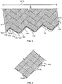
- the braid 10 is formed as a single ply member or element.
- a plurality of solid strands 12 e.g., 12a, 12b, 12c, ... 12g
- a plurality of bundles 14 e.g., 14a, 14b, 14c, ... 14m
- the braid 10 is formed as a single braided or interweaved layer (indicated generally at 16) in which each of the separate elements or, as in the present instance, strands 12 and bundles 14 are single ply.
- a present material for the desoldering braid 10 is copper.
- the configuration of the present braid 10 is in contrast to known braids in which the braided elements (i.e., tubes) are flattened which results in a two-ply configuration.
- a present braid 10 there are seven (7) strands 12 in each bundle 14, and thirteen (13) bundles 14 braided together to form the braid 10.
- the strands 12 are 42 gauge wire. This produces a 13-7-42 braid.
- the braid 10 is formed (or woven) in a 2 over 2 configuration (indicated generally at 18) in which a bundle 14a is passed over (or passed under) the next two adjacent bundles 14b, 14c to form the woven braid 10.
- Such a braid 10 has a width w of about 0.083 inches ( ⁇ 0.010 inches) (2.1 mm ⁇ 0.25 mm) and a thickness t of about 0.014 inches ( ⁇ 0.003 inches) (0.35mm ⁇ 0.08 mm).
- braid 10 can be formed as 13-7-42 braids (13 bundles of seven strands of 42 gauge wire), 13-5-42 braids (13 bundles of five strands of 42 gauge wire) and 13-7-40 braids (13 bundles of seven strands of 40 gauge wire), as well as other sizes, numbers and configurations.
- the number of strands 12 can vary from about 4 to 12 strands per bundle 14, the wire (strand 12) gauge from about 40 to about 44 and the number of bundles 14 per braid 10 from about 9 to about 17.
- This present braided configuration contains about 20 to 24 picks per inch (7,87 to 9,45 picks per cm) and measures about 0.083' (2.1 mm) wide by 0.014' (0.35 mm) thick. A pick is the distance between intersecting bundles (of wire).
- the present single thickness or single ply braid 10 (which resembles a ribbon), is unlike known desoldering braids having a 2-ply construction, in that the known braids are fabrication from a flattened tubular construction. It has been observed that considerably faster heat transfer (a greater heat transfer rate) occurs for melting lead-free solder when the single-ply braid is used for desoldering. This increases the speed and efficiency of the rework process and minimizes heat damage to the printed circuit board (PCB) and components. It has been found that the present braid functions to effectively remove solders having a melting point greater than about 183°C (about 361°F).
- FIG. 4 An alternate braid 110 is illustrated in FIG. 4 .
- This braid is formed in a 1 over 1 configuration in which a bundle 114a alternates over and under each adjacent bundle 114b, 114c.
- the braid 10, 110 can include a flux (indicated generally at 20), such as a high-temperature no clean flux.
- a flux (indicated generally at 20), such as a high-temperature no clean flux.
- One suitable flux 20 is a no clean flux, varieties of which are commercially available, and can be suitably selected from Alpha Metals of Jersey City, New Jersey. This permits desoldering applications using higher temperatures, up to 400° C (752°F). Desoldering with a flux such as this is optimized without premature loss of flux to volatilization or degradation of the flux at higher temperatures.
- the residues remaining on the surface of the PCB when desoldering is complete are noncorrosive if left on the PCB.
- the residues from desoldering can be easily removed using solvent cleaners, if required.
- Another contemplated flux is a rosin flux.
- soldering braid 10, 110 reduces the time needed to melt lead-free solder when a soldering iron (not shown) is used as a heat source.
- a soldering iron (not shown) is used as a heat source.
- heat is efficiently transferred through the desoldering braid 10, 110 to the solder to achieve the melting point of the solder.
- Solder may be removed in this manner from various locations on the PCB during rework and repair for the replacement of soldered components on the PCB. This technique can also be used to clean excess solder from the pads of the PCB after hot air removal of surface mount components to prepare the surface for the application of solder paste prior to hot air reflow of replacement components.
- the braid 10, 110 may be formed using a flat braiding technique or, alternately, using a maypole braiding technique. All such braiding techniques are within the scope of the present invention.
Landscapes
- Engineering & Computer Science (AREA)
- Mechanical Engineering (AREA)
- Manufacturing & Machinery (AREA)
- Textile Engineering (AREA)
- Microelectronics & Electronic Packaging (AREA)
- Electric Connection Of Electric Components To Printed Circuits (AREA)
- Braiding, Manufacturing Of Bobbin-Net Or Lace, And Manufacturing Of Nets By Knotting (AREA)
- Manufacturing Of Printed Wiring (AREA)
Abstract
Claims (10)
- Procédé de dessoudage d'une carte de circuit imprimé ou d'un composant électrique qui présente une soudure sans plomb, le procédé comprenant les étapes qui consistent à :prévoir une tresse en ruban comprenant plusieurs brins en métal plein regroupés pour former un faisceau et plusieurs faisceaux regroupés les uns avec les autres pour former une tresse en ruban etdessouder la carte de circuit imprimé ou le composant électrique de la tresse en ruban,
caractérisé en ce quela tresse est une tresse en ruban en couche unique eten ce que la carte de circuit imprimé ou le composant électrique présentent une soudure sans plomb dont la température de fusion est supérieure à 183°C (environ 361°F) . - Procédé selon la revendication 1, dans lequel les brins métalliques sont en cuivre.
- Procédé selon la revendication 1, comprenant un revêtement fondant sur la tresse.
- Procédé selon la revendication 3, dans lequel le fondant n'est pas un fondant propre.
- Procédé selon la revendication 3, dans lequel le fondant est un fondant à la colophane.
- Procédé selon la revendication 1, dans lequel le faisceau comprend d'environ 4 à environ 12 brins de fil de cuivre.
- Procédé selon la revendication 6, dans lequel le calibre du fil de cuivre présente est compris entre environ 40 et environ 44.
- Procédé selon la revendication 1, dans lequel la tresse en ruban en couche unique contient d'environ 9 à environ 17 faisceaux de brins.
- Procédé selon la revendication 1, dans lequel la tresse est tressée dans une configuration 2 sur 2.
- Procédé selon la revendication 1, dans lequel la tresse en ruban en couche unique est tressée dans une configuration 1 sur 1.
Applications Claiming Priority (2)
| Application Number | Priority Date | Filing Date | Title |
|---|---|---|---|
| US11/062,187 US20060186172A1 (en) | 2005-02-18 | 2005-02-18 | Lead free desoldering braid |
| PCT/IB2006/050372 WO2006087648A1 (fr) | 2005-02-18 | 2006-02-04 | Tresse a dessouder sans plomb |
Publications (2)
| Publication Number | Publication Date |
|---|---|
| EP1850996A1 EP1850996A1 (fr) | 2007-11-07 |
| EP1850996B1 true EP1850996B1 (fr) | 2012-04-11 |
Family
ID=36581491
Family Applications (1)
| Application Number | Title | Priority Date | Filing Date |
|---|---|---|---|
| EP06710828A Expired - Lifetime EP1850996B1 (fr) | 2005-02-18 | 2006-02-04 | Tresse a dessouder sans plomb |
Country Status (9)
| Country | Link |
|---|---|
| US (1) | US20060186172A1 (fr) |
| EP (1) | EP1850996B1 (fr) |
| JP (1) | JP2008529802A (fr) |
| KR (1) | KR101324629B1 (fr) |
| CN (1) | CN101119824B (fr) |
| CA (1) | CA2595516C (fr) |
| MX (1) | MX2007009785A (fr) |
| TW (1) | TWI322733B (fr) |
| WO (1) | WO2006087648A1 (fr) |
Families Citing this family (9)
| Publication number | Priority date | Publication date | Assignee | Title |
|---|---|---|---|---|
| US20060081680A1 (en) * | 2004-10-14 | 2006-04-20 | Kayoko Yoshimura | Desoldering wick for lead-free solder |
| WO2007114334A1 (fr) * | 2006-03-31 | 2007-10-11 | Matsushita Electric Industrial Co., Ltd. | Carte de circuit imprime, procede d'essai de carte de circuit imprime et procede de fabrication de carte de circuit imprime |
| US7780058B2 (en) * | 2008-02-27 | 2010-08-24 | Siuyoung Yao | Braided solder |
| NO336644B1 (no) | 2011-03-29 | 2015-10-12 | Mørenot As | Kappe for et langstrakt legeme |
| US11039787B2 (en) * | 2011-11-23 | 2021-06-22 | Scanmed, Llc | Garment MRI antenna array |
| CN104178914A (zh) * | 2014-07-30 | 2014-12-03 | 华南理工大学 | 一种将长纤维丝材编织成形制造结构件的方法 |
| CN104759726A (zh) * | 2015-03-16 | 2015-07-08 | 成都凯天电子股份有限公司 | 带底部端子封装元器件的解焊方法 |
| US12064827B1 (en) * | 2021-06-13 | 2024-08-20 | Garvey Holding LLC | Methods, systems, and apparatus for joining metallic fabrics |
| CN113319396A (zh) * | 2021-06-15 | 2021-08-31 | 西安微电子技术研究所 | 一种3d叠层封装器件的无损返修装置及方法 |
Family Cites Families (40)
| Publication number | Priority date | Publication date | Assignee | Title |
|---|---|---|---|---|
| US1428976A (en) * | 1918-12-07 | 1922-09-12 | Frank E Payne | Metallic packing |
| US1438940A (en) * | 1920-05-12 | 1922-12-19 | Western Electric Co | Wiredrawing die |
| US2164286A (en) * | 1937-03-22 | 1939-06-27 | Internat Steel Wool Corp | Metallic wool abrading ring |
| US2608124A (en) * | 1946-06-22 | 1952-08-26 | Norman C Jeckel | Braided product and method for producing the same |
| US2694852A (en) * | 1951-01-13 | 1954-11-23 | Riley Stoker Corp | Method of brazing and the product thereof |
| US2800524A (en) * | 1953-07-08 | 1957-07-23 | Glenwood M Van Lear | Electric cable |
| US2957101A (en) * | 1957-06-18 | 1960-10-18 | Evans Reamer And Machine Compa | Electrical contactor device for continuous feed, consumable electrodetype welding apparatus |
| US3627191A (en) * | 1968-03-18 | 1971-12-14 | Jesse Carl Hood Jr | Solder wick |
| US3715797A (en) * | 1970-10-23 | 1973-02-13 | Wik It Electronics Corp | Method for solder removal |
| GB1512015A (en) * | 1974-07-05 | 1978-05-24 | French & Sons Thomas | Braided electrical tape |
| US4051324A (en) * | 1975-05-12 | 1977-09-27 | Haveg Industries, Inc. | Radiation resistant cable and method of making same |
| GB1513496A (en) * | 1976-10-18 | 1978-06-07 | Spirig Ernst | Method of and means for desoldering |
| CH609768A5 (fr) * | 1976-12-22 | 1979-03-15 | Zumbach Electronic Ag | |
| US4164606A (en) * | 1977-11-08 | 1979-08-14 | Ernst Spirig | Tinned copper braids for solder removing |
| GB2094692B (en) * | 1981-03-16 | 1985-08-07 | Spirig Ernst | Desoldering wicks |
| US4416408A (en) * | 1981-05-22 | 1983-11-22 | Ernst Spirig | Solder removing device |
| US4637542A (en) * | 1982-09-22 | 1987-01-20 | Control Data Corporation | Process for soldering and desoldering apertured leadless packages |
| US4518110A (en) * | 1982-09-22 | 1985-05-21 | Control Data Corporation | Device for soldering/desoldering apertured lendless packages |
| US4574994A (en) * | 1983-05-16 | 1986-03-11 | Rauchwerger George P | High speed desoldering tool |
| US4765229A (en) * | 1984-07-02 | 1988-08-23 | Fortune William S | Portable vacuum pump for desoldering purposes |
| US4568011A (en) * | 1984-12-14 | 1986-02-04 | Dearmitt Clyde B | Vacuum pump for desoldering gun |
| US4746050A (en) * | 1987-01-20 | 1988-05-24 | Frank Brown | Solder removal devices |
| US4768699A (en) * | 1987-11-06 | 1988-09-06 | Pace Incorporated | Quick start desoldering method and apparatus |
| US4922083A (en) * | 1988-04-22 | 1990-05-01 | Thermon Manufacturing Company | Flexible, elongated positive temperature coefficient heating assembly and method |
| US5052611A (en) * | 1989-04-20 | 1991-10-01 | Indium Corporation Of America, Inc. | Method of forming a gasket of indium and braid |
| US4934582A (en) * | 1989-09-20 | 1990-06-19 | Microelectronics And Computer Technology Corporation | Method and apparatus for removing solder mounted electronic components |
| US5094139A (en) * | 1990-02-26 | 1992-03-10 | Solder Removal Company | Desoldering braid |
| US5305941A (en) * | 1992-12-28 | 1994-04-26 | Plato Products, Inc. | Desoldering wick |
| US5378290A (en) * | 1993-08-20 | 1995-01-03 | Morgan Crucible Company Plc | Flux |
| US5553768A (en) * | 1993-09-21 | 1996-09-10 | Air-Vac Engineering Company, Inc. | Heat-control process and apparatus for attachment/detachment of soldered components |
| US5544803A (en) * | 1994-08-08 | 1996-08-13 | Cooper Industries, Inc. | Portable electric desoldering tool |
| JPH08215835A (ja) * | 1995-02-13 | 1996-08-27 | Sony Corp | 半田吸引装置 |
| FI950885A0 (fi) * | 1995-02-27 | 1995-02-27 | Sunds Defibrator Woodhandling | Foerfarande foer reglering av flislaengd, skivhugg och skivhuggs skiva |
| JPH09172254A (ja) * | 1995-12-19 | 1997-06-30 | Taiyo Denki Sangyo Kk | ハンダ吸取線 |
| US6057527A (en) * | 1998-06-22 | 2000-05-02 | Cooper Technologies Company | Portable electric desoldering tool |
| JP3019848B1 (ja) * | 1998-11-13 | 2000-03-13 | 日本電気株式会社 | 半導体パッケージの取り外し方法 |
| US6301436B1 (en) * | 2000-10-12 | 2001-10-09 | Yu-Ju Hsiao | Photothermic desoldering unit |
| JP2004154864A (ja) * | 2002-10-15 | 2004-06-03 | Senju Metal Ind Co Ltd | 鉛フリーはんだ合金 |
| JP2005040846A (ja) * | 2003-07-25 | 2005-02-17 | Koyo Senzai Kk | 金属接合用機器 |
| US20060081680A1 (en) * | 2004-10-14 | 2006-04-20 | Kayoko Yoshimura | Desoldering wick for lead-free solder |
-
2005
- 2005-02-18 US US11/062,187 patent/US20060186172A1/en not_active Abandoned
-
2006
- 2006-02-04 EP EP06710828A patent/EP1850996B1/fr not_active Expired - Lifetime
- 2006-02-04 KR KR1020077017817A patent/KR101324629B1/ko not_active Expired - Lifetime
- 2006-02-04 MX MX2007009785A patent/MX2007009785A/es not_active Application Discontinuation
- 2006-02-04 JP JP2007555735A patent/JP2008529802A/ja active Pending
- 2006-02-04 CA CA2595516A patent/CA2595516C/fr not_active Expired - Lifetime
- 2006-02-04 WO PCT/IB2006/050372 patent/WO2006087648A1/fr not_active Ceased
- 2006-02-04 CN CN200680004742.5A patent/CN101119824B/zh not_active Expired - Lifetime
- 2006-02-13 TW TW095104779A patent/TWI322733B/zh not_active IP Right Cessation
Also Published As
| Publication number | Publication date |
|---|---|
| MX2007009785A (es) | 2007-08-22 |
| CA2595516C (fr) | 2012-04-10 |
| US20060186172A1 (en) | 2006-08-24 |
| KR101324629B1 (ko) | 2013-11-04 |
| EP1850996A1 (fr) | 2007-11-07 |
| KR20070104900A (ko) | 2007-10-29 |
| TW200630176A (en) | 2006-09-01 |
| CA2595516A1 (fr) | 2006-08-24 |
| WO2006087648A1 (fr) | 2006-08-24 |
| TWI322733B (en) | 2010-04-01 |
| CN101119824A (zh) | 2008-02-06 |
| JP2008529802A (ja) | 2008-08-07 |
| CN101119824B (zh) | 2014-05-14 |
Similar Documents
| Publication | Publication Date | Title |
|---|---|---|
| JP4553982B2 (ja) | 照明装置及びその製造方法 | |
| CA2595516C (fr) | Tresse a dessouder sans plomb | |
| WO1996025837A1 (fr) | Dispositif et procede de formation et de fixation d'un reseau de globules conducteurs | |
| JP2009218552A (ja) | チップ抵抗器およびその製造方法 | |
| US4345814A (en) | Solder-bearing lead having solder flow-control stop means | |
| US20060285279A1 (en) | Micro solder pot | |
| KR100899251B1 (ko) | 실장 구조체 | |
| JPH0129629B2 (fr) | ||
| WO2020188718A1 (fr) | Carte de circuit imprimé et dispositif électronique | |
| JP5245276B2 (ja) | 電子部品の実装構造及びその実装方法 | |
| TW511403B (en) | Circuit board and electronic equipment using the same | |
| CN110560861A (zh) | 一种电机绕组多层导体的点焊方法 | |
| O’Neill et al. | Addressing Low-Temperature Rework Concerns | |
| JP2013016765A (ja) | はんだ吸い取りシート | |
| JPH05191035A (ja) | 半田ブリッジ除去方法とその装置並びに半田除去用櫛状金属板 | |
| JP5185831B2 (ja) | コンポーネントを順序付けて固定することによる電子モジュールの生産方法 | |
| JP2011036909A (ja) | 半田コテ | |
| JP2005056802A (ja) | ストラップソルダテープ | |
| CN101471268A (zh) | 元件堆叠结构及其装配方法 | |
| JP4716183B2 (ja) | プリント配線基板及び電気機器 | |
| JP4569361B2 (ja) | 回路板及びレーザはんだ付け方法 | |
| JP2018006416A (ja) | 評価用部品、電子基板、及び電子基板生産システム | |
| JP2007180255A (ja) | プリント配線板および代替パッド | |
| Campuzano-Contreras | Assembly of JCAA/JG-PP Test Vehicles | |
| JP2013254983A (ja) | チップ抵抗器およびその製造方法 |
Legal Events
| Date | Code | Title | Description |
|---|---|---|---|
| PUAI | Public reference made under article 153(3) epc to a published international application that has entered the european phase |
Free format text: ORIGINAL CODE: 0009012 |
|
| 17P | Request for examination filed |
Effective date: 20070910 |
|
| AK | Designated contracting states |
Kind code of ref document: A1 Designated state(s): DE FR GB IE |
|
| DAX | Request for extension of the european patent (deleted) | ||
| RBV | Designated contracting states (corrected) |
Designated state(s): DE FR GB IE |
|
| 17Q | First examination report despatched |
Effective date: 20081120 |
|
| GRAP | Despatch of communication of intention to grant a patent |
Free format text: ORIGINAL CODE: EPIDOSNIGR1 |
|
| GRAS | Grant fee paid |
Free format text: ORIGINAL CODE: EPIDOSNIGR3 |
|
| GRAA | (expected) grant |
Free format text: ORIGINAL CODE: 0009210 |
|
| AK | Designated contracting states |
Kind code of ref document: B1 Designated state(s): DE FR GB IE |
|
| REG | Reference to a national code |
Ref country code: GB Ref legal event code: FG4D |
|
| REG | Reference to a national code |
Ref country code: IE Ref legal event code: FG4D |
|
| REG | Reference to a national code |
Ref country code: DE Ref legal event code: R096 Ref document number: 602006028751 Country of ref document: DE Effective date: 20120606 |
|
| PLBE | No opposition filed within time limit |
Free format text: ORIGINAL CODE: 0009261 |
|
| STAA | Information on the status of an ep patent application or granted ep patent |
Free format text: STATUS: NO OPPOSITION FILED WITHIN TIME LIMIT |
|
| 26N | No opposition filed |
Effective date: 20130114 |
|
| REG | Reference to a national code |
Ref country code: DE Ref legal event code: R097 Ref document number: 602006028751 Country of ref document: DE Effective date: 20130114 |
|
| REG | Reference to a national code |
Ref country code: IE Ref legal event code: MM4A |
|
| PG25 | Lapsed in a contracting state [announced via postgrant information from national office to epo] |
Ref country code: IE Free format text: LAPSE BECAUSE OF NON-PAYMENT OF DUE FEES Effective date: 20130204 |
|
| REG | Reference to a national code |
Ref country code: FR Ref legal event code: PLFP Year of fee payment: 11 |
|
| REG | Reference to a national code |
Ref country code: FR Ref legal event code: PLFP Year of fee payment: 12 |
|
| REG | Reference to a national code |
Ref country code: FR Ref legal event code: PLFP Year of fee payment: 13 |
|
| P01 | Opt-out of the competence of the unified patent court (upc) registered |
Effective date: 20230606 |
|
| PGFP | Annual fee paid to national office [announced via postgrant information from national office to epo] |
Ref country code: DE Payment date: 20250227 Year of fee payment: 20 |
|
| PGFP | Annual fee paid to national office [announced via postgrant information from national office to epo] |
Ref country code: FR Payment date: 20250225 Year of fee payment: 20 |
|
| PGFP | Annual fee paid to national office [announced via postgrant information from national office to epo] |
Ref country code: GB Payment date: 20250227 Year of fee payment: 20 |
|
| REG | Reference to a national code |
Ref country code: DE Ref legal event code: R071 Ref document number: 602006028751 Country of ref document: DE |
|
| REG | Reference to a national code |
Ref country code: GB Ref legal event code: PE20 Expiry date: 20260203 |