EP1848045A2 - Housing for semiconductor light emitting or receiving device - Google Patents
Housing for semiconductor light emitting or receiving device Download PDFInfo
- Publication number
- EP1848045A2 EP1848045A2 EP07106416A EP07106416A EP1848045A2 EP 1848045 A2 EP1848045 A2 EP 1848045A2 EP 07106416 A EP07106416 A EP 07106416A EP 07106416 A EP07106416 A EP 07106416A EP 1848045 A2 EP1848045 A2 EP 1848045A2
- Authority
- EP
- European Patent Office
- Prior art keywords
- lead electrode
- wall
- housing
- electrode
- groove
- Prior art date
- Legal status (The legal status is an assumption and is not a legal conclusion. Google has not performed a legal analysis and makes no representation as to the accuracy of the status listed.)
- Granted
Links
- 239000004065 semiconductor Substances 0.000 title claims abstract description 150
- 239000012790 adhesive layer Substances 0.000 claims abstract description 16
- 238000005520 cutting process Methods 0.000 claims abstract description 10
- 239000000853 adhesive Substances 0.000 abstract description 59
- 230000001070 adhesive effect Effects 0.000 abstract description 59
- 239000012778 molding material Substances 0.000 description 55
- 229920005989 resin Polymers 0.000 description 34
- 239000011347 resin Substances 0.000 description 34
- 238000000034 method Methods 0.000 description 20
- 239000000463 material Substances 0.000 description 17
- 238000004519 manufacturing process Methods 0.000 description 15
- 230000000740 bleeding effect Effects 0.000 description 10
- 239000000758 substrate Substances 0.000 description 7
- XEEYBQQBJWHFJM-UHFFFAOYSA-N Iron Chemical compound [Fe] XEEYBQQBJWHFJM-UHFFFAOYSA-N 0.000 description 6
- 230000001681 protective effect Effects 0.000 description 6
- BQCADISMDOOEFD-UHFFFAOYSA-N Silver Chemical compound [Ag] BQCADISMDOOEFD-UHFFFAOYSA-N 0.000 description 5
- 238000005452 bending Methods 0.000 description 5
- 230000007547 defect Effects 0.000 description 5
- 229910052751 metal Inorganic materials 0.000 description 5
- 239000002184 metal Substances 0.000 description 5
- 229910052709 silver Inorganic materials 0.000 description 5
- 239000004332 silver Substances 0.000 description 5
- RYGMFSIKBFXOCR-UHFFFAOYSA-N Copper Chemical compound [Cu] RYGMFSIKBFXOCR-UHFFFAOYSA-N 0.000 description 4
- 229910052802 copper Inorganic materials 0.000 description 4
- 239000010949 copper Substances 0.000 description 4
- 230000000694 effects Effects 0.000 description 4
- 239000010410 layer Substances 0.000 description 4
- 238000007789 sealing Methods 0.000 description 4
- RKTYLMNFRDHKIL-UHFFFAOYSA-N copper;5,10,15,20-tetraphenylporphyrin-22,24-diide Chemical compound [Cu+2].C1=CC(C(=C2C=CC([N-]2)=C(C=2C=CC=CC=2)C=2C=CC(N=2)=C(C=2C=CC=CC=2)C2=CC=C3[N-]2)C=2C=CC=CC=2)=NC1=C3C1=CC=CC=C1 RKTYLMNFRDHKIL-UHFFFAOYSA-N 0.000 description 3
- 239000003822 epoxy resin Substances 0.000 description 3
- 229910052742 iron Inorganic materials 0.000 description 3
- 238000000465 moulding Methods 0.000 description 3
- 229920000647 polyepoxide Polymers 0.000 description 3
- 239000004954 Polyphthalamide Substances 0.000 description 2
- 229910052782 aluminium Inorganic materials 0.000 description 2
- XAGFODPZIPBFFR-UHFFFAOYSA-N aluminium Chemical compound [Al] XAGFODPZIPBFFR-UHFFFAOYSA-N 0.000 description 2
- PCHJSUWPFVWCPO-UHFFFAOYSA-N gold Chemical compound [Au] PCHJSUWPFVWCPO-UHFFFAOYSA-N 0.000 description 2
- 229910052737 gold Inorganic materials 0.000 description 2
- 239000010931 gold Substances 0.000 description 2
- 229910010272 inorganic material Inorganic materials 0.000 description 2
- 239000011147 inorganic material Substances 0.000 description 2
- 239000007788 liquid Substances 0.000 description 2
- BASFCYQUMIYNBI-UHFFFAOYSA-N platinum Chemical compound [Pt] BASFCYQUMIYNBI-UHFFFAOYSA-N 0.000 description 2
- 229920001707 polybutylene terephthalate Polymers 0.000 description 2
- 229920006375 polyphtalamide Polymers 0.000 description 2
- 238000003825 pressing Methods 0.000 description 2
- 229920002050 silicone resin Polymers 0.000 description 2
- 238000003892 spreading Methods 0.000 description 2
- 229920000106 Liquid crystal polymer Polymers 0.000 description 1
- 239000004977 Liquid-crystal polymers (LCPs) Substances 0.000 description 1
- VYPSYNLAJGMNEJ-UHFFFAOYSA-N Silicium dioxide Chemical compound O=[Si]=O VYPSYNLAJGMNEJ-UHFFFAOYSA-N 0.000 description 1
- ATJFFYVFTNAWJD-UHFFFAOYSA-N Tin Chemical compound [Sn] ATJFFYVFTNAWJD-UHFFFAOYSA-N 0.000 description 1
- GWEVSGVZZGPLCZ-UHFFFAOYSA-N Titan oxide Chemical compound O=[Ti]=O GWEVSGVZZGPLCZ-UHFFFAOYSA-N 0.000 description 1
- 229920001807 Urea-formaldehyde Polymers 0.000 description 1
- 239000000956 alloy Substances 0.000 description 1
- 229910045601 alloy Inorganic materials 0.000 description 1
- 230000000903 blocking effect Effects 0.000 description 1
- 239000004020 conductor Substances 0.000 description 1
- 239000000470 constituent Substances 0.000 description 1
- 239000013078 crystal Substances 0.000 description 1
- 230000007423 decrease Effects 0.000 description 1
- 230000003247 decreasing effect Effects 0.000 description 1
- 238000005553 drilling Methods 0.000 description 1
- 238000005516 engineering process Methods 0.000 description 1
- 239000011521 glass Substances 0.000 description 1
- 238000003754 machining Methods 0.000 description 1
- 238000002844 melting Methods 0.000 description 1
- 230000008018 melting Effects 0.000 description 1
- 238000002156 mixing Methods 0.000 description 1
- 150000004767 nitrides Chemical class 0.000 description 1
- 230000003287 optical effect Effects 0.000 description 1
- 239000002245 particle Substances 0.000 description 1
- 239000004014 plasticizer Substances 0.000 description 1
- 238000007747 plating Methods 0.000 description 1
- 229910052697 platinum Inorganic materials 0.000 description 1
- -1 polybutylene terephthalate Polymers 0.000 description 1
- 238000004382 potting Methods 0.000 description 1
- 229910052761 rare earth metal Inorganic materials 0.000 description 1
- 238000002310 reflectometry Methods 0.000 description 1
- 230000000630 rising effect Effects 0.000 description 1
- 229910052594 sapphire Inorganic materials 0.000 description 1
- 239000010980 sapphire Substances 0.000 description 1
- 229920006126 semicrystalline polymer Polymers 0.000 description 1
- 239000000741 silica gel Substances 0.000 description 1
- 229910002027 silica gel Inorganic materials 0.000 description 1
- 229920005992 thermoplastic resin Polymers 0.000 description 1
- 229910052718 tin Inorganic materials 0.000 description 1
- OGIDPMRJRNCKJF-UHFFFAOYSA-N titanium oxide Inorganic materials [Ti]=O OGIDPMRJRNCKJF-UHFFFAOYSA-N 0.000 description 1
- 239000012463 white pigment Substances 0.000 description 1
Images


Classifications
-
- H—ELECTRICITY
- H01—ELECTRIC ELEMENTS
- H01L—SEMICONDUCTOR DEVICES NOT COVERED BY CLASS H10
- H01L33/00—Semiconductor devices with at least one potential-jump barrier or surface barrier specially adapted for light emission; Processes or apparatus specially adapted for the manufacture or treatment thereof or of parts thereof; Details thereof
- H01L33/48—Semiconductor devices with at least one potential-jump barrier or surface barrier specially adapted for light emission; Processes or apparatus specially adapted for the manufacture or treatment thereof or of parts thereof; Details thereof characterised by the semiconductor body packages
- H01L33/483—Containers
- H01L33/486—Containers adapted for surface mounting
-
- B—PERFORMING OPERATIONS; TRANSPORTING
- B29—WORKING OF PLASTICS; WORKING OF SUBSTANCES IN A PLASTIC STATE IN GENERAL
- B29C—SHAPING OR JOINING OF PLASTICS; SHAPING OF MATERIAL IN A PLASTIC STATE, NOT OTHERWISE PROVIDED FOR; AFTER-TREATMENT OF THE SHAPED PRODUCTS, e.g. REPAIRING
- B29C45/00—Injection moulding, i.e. forcing the required volume of moulding material through a nozzle into a closed mould; Apparatus therefor
- B29C45/14—Injection moulding, i.e. forcing the required volume of moulding material through a nozzle into a closed mould; Apparatus therefor incorporating preformed parts or layers, e.g. injection moulding around inserts or for coating articles
- B29C45/14639—Injection moulding, i.e. forcing the required volume of moulding material through a nozzle into a closed mould; Apparatus therefor incorporating preformed parts or layers, e.g. injection moulding around inserts or for coating articles for obtaining an insulating effect, e.g. for electrical components
-
- H—ELECTRICITY
- H01—ELECTRIC ELEMENTS
- H01L—SEMICONDUCTOR DEVICES NOT COVERED BY CLASS H10
- H01L23/00—Details of semiconductor or other solid state devices
- H01L23/48—Arrangements for conducting electric current to or from the solid state body in operation, e.g. leads, terminal arrangements ; Selection of materials therefor
- H01L23/488—Arrangements for conducting electric current to or from the solid state body in operation, e.g. leads, terminal arrangements ; Selection of materials therefor consisting of soldered or bonded constructions
- H01L23/498—Leads, i.e. metallisations or lead-frames on insulating substrates, e.g. chip carriers
- H01L23/49861—Lead-frames fixed on or encapsulated in insulating substrates
-
- H—ELECTRICITY
- H01—ELECTRIC ELEMENTS
- H01L—SEMICONDUCTOR DEVICES NOT COVERED BY CLASS H10
- H01L24/00—Arrangements for connecting or disconnecting semiconductor or solid-state bodies; Methods or apparatus related thereto
- H01L24/01—Means for bonding being attached to, or being formed on, the surface to be connected, e.g. chip-to-package, die-attach, "first-level" interconnects; Manufacturing methods related thereto
- H01L24/42—Wire connectors; Manufacturing methods related thereto
- H01L24/47—Structure, shape, material or disposition of the wire connectors after the connecting process
- H01L24/48—Structure, shape, material or disposition of the wire connectors after the connecting process of an individual wire connector
-
- H—ELECTRICITY
- H01—ELECTRIC ELEMENTS
- H01L—SEMICONDUCTOR DEVICES NOT COVERED BY CLASS H10
- H01L33/00—Semiconductor devices with at least one potential-jump barrier or surface barrier specially adapted for light emission; Processes or apparatus specially adapted for the manufacture or treatment thereof or of parts thereof; Details thereof
- H01L33/48—Semiconductor devices with at least one potential-jump barrier or surface barrier specially adapted for light emission; Processes or apparatus specially adapted for the manufacture or treatment thereof or of parts thereof; Details thereof characterised by the semiconductor body packages
- H01L33/62—Arrangements for conducting electric current to or from the semiconductor body, e.g. lead-frames, wire-bonds or solder balls
-
- H—ELECTRICITY
- H01—ELECTRIC ELEMENTS
- H01L—SEMICONDUCTOR DEVICES NOT COVERED BY CLASS H10
- H01L2224/00—Indexing scheme for arrangements for connecting or disconnecting semiconductor or solid-state bodies and methods related thereto as covered by H01L24/00
- H01L2224/01—Means for bonding being attached to, or being formed on, the surface to be connected, e.g. chip-to-package, die-attach, "first-level" interconnects; Manufacturing methods related thereto
- H01L2224/26—Layer connectors, e.g. plate connectors, solder or adhesive layers; Manufacturing methods related thereto
- H01L2224/31—Structure, shape, material or disposition of the layer connectors after the connecting process
- H01L2224/32—Structure, shape, material or disposition of the layer connectors after the connecting process of an individual layer connector
- H01L2224/321—Disposition
- H01L2224/32151—Disposition the layer connector connecting between a semiconductor or solid-state body and an item not being a semiconductor or solid-state body, e.g. chip-to-substrate, chip-to-passive
- H01L2224/32221—Disposition the layer connector connecting between a semiconductor or solid-state body and an item not being a semiconductor or solid-state body, e.g. chip-to-substrate, chip-to-passive the body and the item being stacked
- H01L2224/32245—Disposition the layer connector connecting between a semiconductor or solid-state body and an item not being a semiconductor or solid-state body, e.g. chip-to-substrate, chip-to-passive the body and the item being stacked the item being metallic
-
- H—ELECTRICITY
- H01—ELECTRIC ELEMENTS
- H01L—SEMICONDUCTOR DEVICES NOT COVERED BY CLASS H10
- H01L2224/00—Indexing scheme for arrangements for connecting or disconnecting semiconductor or solid-state bodies and methods related thereto as covered by H01L24/00
- H01L2224/01—Means for bonding being attached to, or being formed on, the surface to be connected, e.g. chip-to-package, die-attach, "first-level" interconnects; Manufacturing methods related thereto
- H01L2224/42—Wire connectors; Manufacturing methods related thereto
- H01L2224/44—Structure, shape, material or disposition of the wire connectors prior to the connecting process
- H01L2224/45—Structure, shape, material or disposition of the wire connectors prior to the connecting process of an individual wire connector
- H01L2224/45001—Core members of the connector
- H01L2224/45099—Material
- H01L2224/451—Material with a principal constituent of the material being a metal or a metalloid, e.g. boron (B), silicon (Si), germanium (Ge), arsenic (As), antimony (Sb), tellurium (Te) and polonium (Po), and alloys thereof
- H01L2224/45117—Material with a principal constituent of the material being a metal or a metalloid, e.g. boron (B), silicon (Si), germanium (Ge), arsenic (As), antimony (Sb), tellurium (Te) and polonium (Po), and alloys thereof the principal constituent melting at a temperature of greater than or equal to 400°C and less than 950°C
- H01L2224/45124—Aluminium (Al) as principal constituent
-
- H—ELECTRICITY
- H01—ELECTRIC ELEMENTS
- H01L—SEMICONDUCTOR DEVICES NOT COVERED BY CLASS H10
- H01L2224/00—Indexing scheme for arrangements for connecting or disconnecting semiconductor or solid-state bodies and methods related thereto as covered by H01L24/00
- H01L2224/01—Means for bonding being attached to, or being formed on, the surface to be connected, e.g. chip-to-package, die-attach, "first-level" interconnects; Manufacturing methods related thereto
- H01L2224/42—Wire connectors; Manufacturing methods related thereto
- H01L2224/44—Structure, shape, material or disposition of the wire connectors prior to the connecting process
- H01L2224/45—Structure, shape, material or disposition of the wire connectors prior to the connecting process of an individual wire connector
- H01L2224/45001—Core members of the connector
- H01L2224/45099—Material
- H01L2224/451—Material with a principal constituent of the material being a metal or a metalloid, e.g. boron (B), silicon (Si), germanium (Ge), arsenic (As), antimony (Sb), tellurium (Te) and polonium (Po), and alloys thereof
- H01L2224/45138—Material with a principal constituent of the material being a metal or a metalloid, e.g. boron (B), silicon (Si), germanium (Ge), arsenic (As), antimony (Sb), tellurium (Te) and polonium (Po), and alloys thereof the principal constituent melting at a temperature of greater than or equal to 950°C and less than 1550°C
- H01L2224/45144—Gold (Au) as principal constituent
-
- H—ELECTRICITY
- H01—ELECTRIC ELEMENTS
- H01L—SEMICONDUCTOR DEVICES NOT COVERED BY CLASS H10
- H01L2224/00—Indexing scheme for arrangements for connecting or disconnecting semiconductor or solid-state bodies and methods related thereto as covered by H01L24/00
- H01L2224/01—Means for bonding being attached to, or being formed on, the surface to be connected, e.g. chip-to-package, die-attach, "first-level" interconnects; Manufacturing methods related thereto
- H01L2224/42—Wire connectors; Manufacturing methods related thereto
- H01L2224/44—Structure, shape, material or disposition of the wire connectors prior to the connecting process
- H01L2224/45—Structure, shape, material or disposition of the wire connectors prior to the connecting process of an individual wire connector
- H01L2224/45001—Core members of the connector
- H01L2224/45099—Material
- H01L2224/451—Material with a principal constituent of the material being a metal or a metalloid, e.g. boron (B), silicon (Si), germanium (Ge), arsenic (As), antimony (Sb), tellurium (Te) and polonium (Po), and alloys thereof
- H01L2224/45138—Material with a principal constituent of the material being a metal or a metalloid, e.g. boron (B), silicon (Si), germanium (Ge), arsenic (As), antimony (Sb), tellurium (Te) and polonium (Po), and alloys thereof the principal constituent melting at a temperature of greater than or equal to 950°C and less than 1550°C
- H01L2224/45147—Copper (Cu) as principal constituent
-
- H—ELECTRICITY
- H01—ELECTRIC ELEMENTS
- H01L—SEMICONDUCTOR DEVICES NOT COVERED BY CLASS H10
- H01L2224/00—Indexing scheme for arrangements for connecting or disconnecting semiconductor or solid-state bodies and methods related thereto as covered by H01L24/00
- H01L2224/01—Means for bonding being attached to, or being formed on, the surface to be connected, e.g. chip-to-package, die-attach, "first-level" interconnects; Manufacturing methods related thereto
- H01L2224/42—Wire connectors; Manufacturing methods related thereto
- H01L2224/44—Structure, shape, material or disposition of the wire connectors prior to the connecting process
- H01L2224/45—Structure, shape, material or disposition of the wire connectors prior to the connecting process of an individual wire connector
- H01L2224/45001—Core members of the connector
- H01L2224/45099—Material
- H01L2224/451—Material with a principal constituent of the material being a metal or a metalloid, e.g. boron (B), silicon (Si), germanium (Ge), arsenic (As), antimony (Sb), tellurium (Te) and polonium (Po), and alloys thereof
- H01L2224/45163—Material with a principal constituent of the material being a metal or a metalloid, e.g. boron (B), silicon (Si), germanium (Ge), arsenic (As), antimony (Sb), tellurium (Te) and polonium (Po), and alloys thereof the principal constituent melting at a temperature of greater than 1550°C
- H01L2224/45169—Platinum (Pt) as principal constituent
-
- H—ELECTRICITY
- H01—ELECTRIC ELEMENTS
- H01L—SEMICONDUCTOR DEVICES NOT COVERED BY CLASS H10
- H01L2224/00—Indexing scheme for arrangements for connecting or disconnecting semiconductor or solid-state bodies and methods related thereto as covered by H01L24/00
- H01L2224/01—Means for bonding being attached to, or being formed on, the surface to be connected, e.g. chip-to-package, die-attach, "first-level" interconnects; Manufacturing methods related thereto
- H01L2224/42—Wire connectors; Manufacturing methods related thereto
- H01L2224/47—Structure, shape, material or disposition of the wire connectors after the connecting process
- H01L2224/48—Structure, shape, material or disposition of the wire connectors after the connecting process of an individual wire connector
- H01L2224/4805—Shape
- H01L2224/4809—Loop shape
- H01L2224/48091—Arched
-
- H—ELECTRICITY
- H01—ELECTRIC ELEMENTS
- H01L—SEMICONDUCTOR DEVICES NOT COVERED BY CLASS H10
- H01L2224/00—Indexing scheme for arrangements for connecting or disconnecting semiconductor or solid-state bodies and methods related thereto as covered by H01L24/00
- H01L2224/01—Means for bonding being attached to, or being formed on, the surface to be connected, e.g. chip-to-package, die-attach, "first-level" interconnects; Manufacturing methods related thereto
- H01L2224/42—Wire connectors; Manufacturing methods related thereto
- H01L2224/47—Structure, shape, material or disposition of the wire connectors after the connecting process
- H01L2224/48—Structure, shape, material or disposition of the wire connectors after the connecting process of an individual wire connector
- H01L2224/4805—Shape
- H01L2224/4809—Loop shape
- H01L2224/48095—Kinked
- H01L2224/48097—Kinked the kinked part being in proximity to the bonding area outside the semiconductor or solid-state body
-
- H—ELECTRICITY
- H01—ELECTRIC ELEMENTS
- H01L—SEMICONDUCTOR DEVICES NOT COVERED BY CLASS H10
- H01L2224/00—Indexing scheme for arrangements for connecting or disconnecting semiconductor or solid-state bodies and methods related thereto as covered by H01L24/00
- H01L2224/01—Means for bonding being attached to, or being formed on, the surface to be connected, e.g. chip-to-package, die-attach, "first-level" interconnects; Manufacturing methods related thereto
- H01L2224/42—Wire connectors; Manufacturing methods related thereto
- H01L2224/47—Structure, shape, material or disposition of the wire connectors after the connecting process
- H01L2224/48—Structure, shape, material or disposition of the wire connectors after the connecting process of an individual wire connector
- H01L2224/481—Disposition
- H01L2224/48151—Connecting between a semiconductor or solid-state body and an item not being a semiconductor or solid-state body, e.g. chip-to-substrate, chip-to-passive
- H01L2224/48221—Connecting between a semiconductor or solid-state body and an item not being a semiconductor or solid-state body, e.g. chip-to-substrate, chip-to-passive the body and the item being stacked
- H01L2224/48245—Connecting between a semiconductor or solid-state body and an item not being a semiconductor or solid-state body, e.g. chip-to-substrate, chip-to-passive the body and the item being stacked the item being metallic
- H01L2224/48247—Connecting between a semiconductor or solid-state body and an item not being a semiconductor or solid-state body, e.g. chip-to-substrate, chip-to-passive the body and the item being stacked the item being metallic connecting the wire to a bond pad of the item
-
- H—ELECTRICITY
- H01—ELECTRIC ELEMENTS
- H01L—SEMICONDUCTOR DEVICES NOT COVERED BY CLASS H10
- H01L2224/00—Indexing scheme for arrangements for connecting or disconnecting semiconductor or solid-state bodies and methods related thereto as covered by H01L24/00
- H01L2224/01—Means for bonding being attached to, or being formed on, the surface to be connected, e.g. chip-to-package, die-attach, "first-level" interconnects; Manufacturing methods related thereto
- H01L2224/42—Wire connectors; Manufacturing methods related thereto
- H01L2224/47—Structure, shape, material or disposition of the wire connectors after the connecting process
- H01L2224/48—Structure, shape, material or disposition of the wire connectors after the connecting process of an individual wire connector
- H01L2224/484—Connecting portions
- H01L2224/48463—Connecting portions the connecting portion on the bonding area of the semiconductor or solid-state body being a ball bond
- H01L2224/48465—Connecting portions the connecting portion on the bonding area of the semiconductor or solid-state body being a ball bond the other connecting portion not on the bonding area being a wedge bond, i.e. ball-to-wedge, regular stitch
-
- H—ELECTRICITY
- H01—ELECTRIC ELEMENTS
- H01L—SEMICONDUCTOR DEVICES NOT COVERED BY CLASS H10
- H01L2224/00—Indexing scheme for arrangements for connecting or disconnecting semiconductor or solid-state bodies and methods related thereto as covered by H01L24/00
- H01L2224/01—Means for bonding being attached to, or being formed on, the surface to be connected, e.g. chip-to-package, die-attach, "first-level" interconnects; Manufacturing methods related thereto
- H01L2224/42—Wire connectors; Manufacturing methods related thereto
- H01L2224/47—Structure, shape, material or disposition of the wire connectors after the connecting process
- H01L2224/48—Structure, shape, material or disposition of the wire connectors after the connecting process of an individual wire connector
- H01L2224/4899—Auxiliary members for wire connectors, e.g. flow-barriers, reinforcing structures, spacers, alignment aids
- H01L2224/48996—Auxiliary members for wire connectors, e.g. flow-barriers, reinforcing structures, spacers, alignment aids being formed on an item to be connected not being a semiconductor or solid-state body
- H01L2224/48997—Reinforcing structures
-
- H—ELECTRICITY
- H01—ELECTRIC ELEMENTS
- H01L—SEMICONDUCTOR DEVICES NOT COVERED BY CLASS H10
- H01L2224/00—Indexing scheme for arrangements for connecting or disconnecting semiconductor or solid-state bodies and methods related thereto as covered by H01L24/00
- H01L2224/73—Means for bonding being of different types provided for in two or more of groups H01L2224/10, H01L2224/18, H01L2224/26, H01L2224/34, H01L2224/42, H01L2224/50, H01L2224/63, H01L2224/71
- H01L2224/732—Location after the connecting process
- H01L2224/73251—Location after the connecting process on different surfaces
- H01L2224/73265—Layer and wire connectors
-
- H—ELECTRICITY
- H01—ELECTRIC ELEMENTS
- H01L—SEMICONDUCTOR DEVICES NOT COVERED BY CLASS H10
- H01L2224/00—Indexing scheme for arrangements for connecting or disconnecting semiconductor or solid-state bodies and methods related thereto as covered by H01L24/00
- H01L2224/80—Methods for connecting semiconductor or other solid state bodies using means for bonding being attached to, or being formed on, the surface to be connected
- H01L2224/85—Methods for connecting semiconductor or other solid state bodies using means for bonding being attached to, or being formed on, the surface to be connected using a wire connector
- H01L2224/85909—Post-treatment of the connector or wire bonding area
- H01L2224/85951—Forming additional members, e.g. for reinforcing
-
- H—ELECTRICITY
- H01—ELECTRIC ELEMENTS
- H01L—SEMICONDUCTOR DEVICES NOT COVERED BY CLASS H10
- H01L24/00—Arrangements for connecting or disconnecting semiconductor or solid-state bodies; Methods or apparatus related thereto
- H01L24/01—Means for bonding being attached to, or being formed on, the surface to be connected, e.g. chip-to-package, die-attach, "first-level" interconnects; Manufacturing methods related thereto
- H01L24/42—Wire connectors; Manufacturing methods related thereto
- H01L24/44—Structure, shape, material or disposition of the wire connectors prior to the connecting process
- H01L24/45—Structure, shape, material or disposition of the wire connectors prior to the connecting process of an individual wire connector
-
- H—ELECTRICITY
- H01—ELECTRIC ELEMENTS
- H01L—SEMICONDUCTOR DEVICES NOT COVERED BY CLASS H10
- H01L25/00—Assemblies consisting of a plurality of individual semiconductor or other solid state devices ; Multistep manufacturing processes thereof
- H01L25/16—Assemblies consisting of a plurality of individual semiconductor or other solid state devices ; Multistep manufacturing processes thereof the devices being of types provided for in two or more different main groups of groups H01L27/00 - H01L33/00, or in a single subclass of H10K, H10N, e.g. forming hybrid circuits
- H01L25/167—Assemblies consisting of a plurality of individual semiconductor or other solid state devices ; Multistep manufacturing processes thereof the devices being of types provided for in two or more different main groups of groups H01L27/00 - H01L33/00, or in a single subclass of H10K, H10N, e.g. forming hybrid circuits comprising optoelectronic devices, e.g. LED, photodiodes
-
- H—ELECTRICITY
- H01—ELECTRIC ELEMENTS
- H01L—SEMICONDUCTOR DEVICES NOT COVERED BY CLASS H10
- H01L2924/00—Indexing scheme for arrangements or methods for connecting or disconnecting semiconductor or solid-state bodies as covered by H01L24/00
- H01L2924/0001—Technical content checked by a classifier
- H01L2924/00014—Technical content checked by a classifier the subject-matter covered by the group, the symbol of which is combined with the symbol of this group, being disclosed without further technical details
-
- H—ELECTRICITY
- H01—ELECTRIC ELEMENTS
- H01L—SEMICONDUCTOR DEVICES NOT COVERED BY CLASS H10
- H01L2924/00—Indexing scheme for arrangements or methods for connecting or disconnecting semiconductor or solid-state bodies as covered by H01L24/00
- H01L2924/01—Chemical elements
- H01L2924/01005—Boron [B]
-
- H—ELECTRICITY
- H01—ELECTRIC ELEMENTS
- H01L—SEMICONDUCTOR DEVICES NOT COVERED BY CLASS H10
- H01L2924/00—Indexing scheme for arrangements or methods for connecting or disconnecting semiconductor or solid-state bodies as covered by H01L24/00
- H01L2924/01—Chemical elements
- H01L2924/01006—Carbon [C]
-
- H—ELECTRICITY
- H01—ELECTRIC ELEMENTS
- H01L—SEMICONDUCTOR DEVICES NOT COVERED BY CLASS H10
- H01L2924/00—Indexing scheme for arrangements or methods for connecting or disconnecting semiconductor or solid-state bodies as covered by H01L24/00
- H01L2924/01—Chemical elements
- H01L2924/01013—Aluminum [Al]
-
- H—ELECTRICITY
- H01—ELECTRIC ELEMENTS
- H01L—SEMICONDUCTOR DEVICES NOT COVERED BY CLASS H10
- H01L2924/00—Indexing scheme for arrangements or methods for connecting or disconnecting semiconductor or solid-state bodies as covered by H01L24/00
- H01L2924/01—Chemical elements
- H01L2924/01023—Vanadium [V]
-
- H—ELECTRICITY
- H01—ELECTRIC ELEMENTS
- H01L—SEMICONDUCTOR DEVICES NOT COVERED BY CLASS H10
- H01L2924/00—Indexing scheme for arrangements or methods for connecting or disconnecting semiconductor or solid-state bodies as covered by H01L24/00
- H01L2924/01—Chemical elements
- H01L2924/01029—Copper [Cu]
-
- H—ELECTRICITY
- H01—ELECTRIC ELEMENTS
- H01L—SEMICONDUCTOR DEVICES NOT COVERED BY CLASS H10
- H01L2924/00—Indexing scheme for arrangements or methods for connecting or disconnecting semiconductor or solid-state bodies as covered by H01L24/00
- H01L2924/01—Chemical elements
- H01L2924/01033—Arsenic [As]
-
- H—ELECTRICITY
- H01—ELECTRIC ELEMENTS
- H01L—SEMICONDUCTOR DEVICES NOT COVERED BY CLASS H10
- H01L2924/00—Indexing scheme for arrangements or methods for connecting or disconnecting semiconductor or solid-state bodies as covered by H01L24/00
- H01L2924/01—Chemical elements
- H01L2924/01047—Silver [Ag]
-
- H—ELECTRICITY
- H01—ELECTRIC ELEMENTS
- H01L—SEMICONDUCTOR DEVICES NOT COVERED BY CLASS H10
- H01L2924/00—Indexing scheme for arrangements or methods for connecting or disconnecting semiconductor or solid-state bodies as covered by H01L24/00
- H01L2924/01—Chemical elements
- H01L2924/0105—Tin [Sn]
-
- H—ELECTRICITY
- H01—ELECTRIC ELEMENTS
- H01L—SEMICONDUCTOR DEVICES NOT COVERED BY CLASS H10
- H01L2924/00—Indexing scheme for arrangements or methods for connecting or disconnecting semiconductor or solid-state bodies as covered by H01L24/00
- H01L2924/01—Chemical elements
- H01L2924/01078—Platinum [Pt]
-
- H—ELECTRICITY
- H01—ELECTRIC ELEMENTS
- H01L—SEMICONDUCTOR DEVICES NOT COVERED BY CLASS H10
- H01L2924/00—Indexing scheme for arrangements or methods for connecting or disconnecting semiconductor or solid-state bodies as covered by H01L24/00
- H01L2924/01—Chemical elements
- H01L2924/01079—Gold [Au]
-
- H—ELECTRICITY
- H01—ELECTRIC ELEMENTS
- H01L—SEMICONDUCTOR DEVICES NOT COVERED BY CLASS H10
- H01L2924/00—Indexing scheme for arrangements or methods for connecting or disconnecting semiconductor or solid-state bodies as covered by H01L24/00
- H01L2924/01—Chemical elements
- H01L2924/01082—Lead [Pb]
-
- H—ELECTRICITY
- H01—ELECTRIC ELEMENTS
- H01L—SEMICONDUCTOR DEVICES NOT COVERED BY CLASS H10
- H01L2924/00—Indexing scheme for arrangements or methods for connecting or disconnecting semiconductor or solid-state bodies as covered by H01L24/00
- H01L2924/06—Polymers
- H01L2924/078—Adhesive characteristics other than chemical
- H01L2924/07802—Adhesive characteristics other than chemical not being an ohmic electrical conductor
-
- H—ELECTRICITY
- H01—ELECTRIC ELEMENTS
- H01L—SEMICONDUCTOR DEVICES NOT COVERED BY CLASS H10
- H01L2924/00—Indexing scheme for arrangements or methods for connecting or disconnecting semiconductor or solid-state bodies as covered by H01L24/00
- H01L2924/10—Details of semiconductor or other solid state devices to be connected
- H01L2924/11—Device type
- H01L2924/12—Passive devices, e.g. 2 terminal devices
- H01L2924/1203—Rectifying Diode
- H01L2924/12035—Zener diode
-
- H—ELECTRICITY
- H01—ELECTRIC ELEMENTS
- H01L—SEMICONDUCTOR DEVICES NOT COVERED BY CLASS H10
- H01L2924/00—Indexing scheme for arrangements or methods for connecting or disconnecting semiconductor or solid-state bodies as covered by H01L24/00
- H01L2924/10—Details of semiconductor or other solid state devices to be connected
- H01L2924/11—Device type
- H01L2924/12—Passive devices, e.g. 2 terminal devices
- H01L2924/1204—Optical Diode
- H01L2924/12041—LED
-
- H—ELECTRICITY
- H01—ELECTRIC ELEMENTS
- H01L—SEMICONDUCTOR DEVICES NOT COVERED BY CLASS H10
- H01L2924/00—Indexing scheme for arrangements or methods for connecting or disconnecting semiconductor or solid-state bodies as covered by H01L24/00
- H01L2924/15—Details of package parts other than the semiconductor or other solid state devices to be connected
- H01L2924/181—Encapsulation
-
- H—ELECTRICITY
- H01—ELECTRIC ELEMENTS
- H01L—SEMICONDUCTOR DEVICES NOT COVERED BY CLASS H10
- H01L2924/00—Indexing scheme for arrangements or methods for connecting or disconnecting semiconductor or solid-state bodies as covered by H01L24/00
- H01L2924/19—Details of hybrid assemblies other than the semiconductor or other solid state devices to be connected
- H01L2924/191—Disposition
- H01L2924/19101—Disposition of discrete passive components
- H01L2924/19107—Disposition of discrete passive components off-chip wires
-
- H—ELECTRICITY
- H01—ELECTRIC ELEMENTS
- H01L—SEMICONDUCTOR DEVICES NOT COVERED BY CLASS H10
- H01L31/00—Semiconductor devices sensitive to infrared radiation, light, electromagnetic radiation of shorter wavelength or corpuscular radiation and specially adapted either for the conversion of the energy of such radiation into electrical energy or for the control of electrical energy by such radiation; Processes or apparatus specially adapted for the manufacture or treatment thereof or of parts thereof; Details thereof
- H01L31/02—Details
- H01L31/0203—Containers; Encapsulations, e.g. encapsulation of photodiodes
Definitions
- the present invention relates to a semiconductor device having a semiconductor element mounted in a housing thereof, and particularly to a semiconductor light emitting device employing a semiconductor light emitting element and a semiconductor light receiving device used as photo sensor or the like.
- Semiconductor devices currently available include a semiconductor light emitting device which has a semiconductor light emitting element mounted in a housing.
- the housing has a recess for accommodating the semiconductor light emitting element, and exposed on the surface of the recess are a pair of lead electrodes which are connected to the electrodes of the semiconductor light emitting element.
- the semiconductor light emitting element is mounted in the housing by die bonding the substrate side of the semiconductor light emitting element onto one of the lead electrodes by means of a silver paste or the like, and connecting the semiconductor side of the semiconductor light emitting element to the other lead electrode by means of an electrically conductive wire.
- the housing As the semiconductor device becomes smaller year by year, the housing also becomes smaller and accordingly the recess of the housing and the lead electrodes exposed in the recess become smaller in size.
- bleeding phenomenon that is to say, flowing the silver paste for die bonding from the one lead electrode to the other lead electrode is likely to occur, eventually causing short circuiting of the semiconductor device. It is known to prevent the bleeding phenomenon by providing a protrusion between the lead electrodes (refer to, for example, Japanese Unexamined Patent Publication (Kokai) No. 10-294495 and Japanese Unexamined Utility Model Publication (Kokai) No. 62-47156 ).
- a first bonding region where die bonding is carried out and a second bonding region where wire bonding is carried out are separated from each other by a wall (refer to, for example, Japanese Unexamined Patent Publication (Kokai) No. 2005-33194).
- the wall prevents the die bonding material for die bonding of the protective element from flowing into the second bonding region.
- the semiconductor element is formed on an insulating substrate such as sapphire, which disables electrical continuity to be established through the substrate. For this reason, both a positive electrode and a negative electrode of the semiconductor light emitting element are formed on the semiconductor side, and are wire bonded to the corresponding lead electrodes when mounting the element. At this time, the semiconductor light emitting element is bonded onto either of the lead electrodes by means of an electrically conductive adhesive such as silver paste or an insulating adhesive such as die bonding resin.
- an electrically conductive adhesive such as silver paste or an insulating adhesive such as die bonding resin.
- the liquid component of the adhesive and the adhesive itself can easily spread over the surface of the lead electrode (which is also bleeding phenomenon) so as to cover the surface of the lead electrode, even when application of the adhesive is limited to the die bonding area of the lead electrode.
- the die bonding area and the wire bonding area are disposed adjacent to each other on the same surface of the same lead electrode, and therefore the adhesive components can very easily overflow. Bleeding phenomenon can occur far more easily in this case than in the prior art in which the lead electrodes are disposed apart from each other.
- the electrically conductive wire connecting the lead electrode and the electrode of the semiconductor light emitting element cannot be fixed sufficiently on the lead electrode when wire bonding, and it becomes impossible to establish electrical continuity by means of the electrically conductive wire in case an insulating adhesive is used.
- Japanese Unexamined Patent Publication (Kokai) No. 10-294495 and Japanese Unexamined Utility Model Publication (Kokai) No. 62-471562 use semiconductor light emitting element having an electrically conductive substrate, and is capable of establishing electrical continuity between the semiconductor light emitting element and the lead electrode while securing the electrically conductive substrate of the semiconductor light emitting element on the lead electrode by die bonding with an adhesive layer consisting of an electrically conductive adhesive. Therefore, while such a structure is provided that prevents bleeding phenomenon between the lead electrodes in order to avoid short circuiting between the two lead electrodes, spreading of the adhesive for die bonding over the surface of the lead electrode to be die bonded does not pose a problem.
- an object of the present invention is to provide a semiconductor device wherein the adhesive components do not overflow nor leak to the wire bonding area even when an adhesive consisting of adhesive components having low surface tension is used in the adhesive layer for die bonding, and the overflow and leak preventing function can be maintained satisfactorily even when the device is made smaller and thinner.
- First aspect of the present invention is a semiconductor device comprising a semiconductor element having a pair of electrodes, a housing having a recess for accommodating the semiconductor element, a first lead electrode and a second lead electrode which are exposed on the bottom of the recess, an adhesive layer for die bonding between the semiconductor element and the first lead electrode, and electrically conductive wires for wire bonding between one electrode of the pair of electrodes of the semiconductor element and the first lead electrode and between the other electrode and the second lead electrode, wherein the housing has at least one wall formed to extend across the bottom surface of the recess so as to divide the surface of the first lead electrode into a die bonding area and a wire bonding area, and the first lead electrode has a cut-out portion which is formed by cutting off a portion of an edge of the lead electrode and located at least just below the wall, while the wall and the bottom portion of the housing are connected to each other through the cut-out portion.
- the cut-out portion is formed just below the first wall, the first wall and the housing can be connected through the cut-out portion, and therefore a cross-sectional area of a connecting portion between them are increased.
- This enables it to improve adhesiveness between the first wall and the surface of the first lead electrode.
- the improved adhesiveness is effective in preventing the adhesive components from leaking to the wire bonding area along the interface between the first lead electrode and the first wall.
- the cut-out portion has also an effect of making the first wall easier to pour the molding material when forming it. The passage through which the molding material flows into the first wall is widened by the cut-out portion.
- the first wall is small in height to such an extent that does not hamper wire bonding, and therefore it is difficult to fill in the molding material which may result in locally insufficient filling in case the molding material has high viscosity.
- forming the cut-out portion widens the passage for filling and makes it easier to fill in with the molding material.
- the cut-out portion may have a form of notch formed by cutting off a portion of the edge of the first lead electrode, or a form of through hole formed in the first lead electrode.
- Second aspect of the present invention is a semiconductor device comprising a semiconductor element having a pair of electrodes, a housing having a recess for accommodating the semiconductor element, a first lead electrode and a second lead electrode which are exposed on the bottom surface of the recess, an adhesive layer for die bonding between the semiconductor element and the first lead electrode, and electrically conductive wires for wire bonding between one electrode of the pair of electrodes of the semiconductor element and the first lead electrode and between the other electrode and the second lead electrode, wherein the housing has at least one wall formed to extend across the bottom surface of the recess so as to divide the surface of the first lead electrode into a die bonding area and a wire bonding area, and the first lead electrode has a groove which is formed in the surface thereof so as to extend along the wall and located at least just below the wall, while the bottom of the wall is engaged with the groove.
- the groove is formed in the surface of the first lead electrode, and the first wall is formed on the groove. Since the groove is formed along the first wall which separates the die bonding area and the wire bonding area, even if the adhesive components of the adhesive for die bonding tend to leak form the die bond area to the wire bonding area along the interface between the first lead electrode and the first wall, the adhesive components are stuck in the groove and cannot proceed further. Thus the groove formed just below the first wall enables it to surely prevent the adhesive component from entering the wire bonding area. Also as the cross section of the first wall is increased by the groove, bonding strength between the first wall and the side wall of the housing is also increased. As the bonding strength is increased, adhesiveness between the first wall and the surface of the first lead electrode can be improved, which is effective in preventing the adhesive components from leaking to the wire bonding area along the interface between the first lead electrode and the first wall.
- the second aspect of the present invention is advantageous also when forming the first wall.
- the groove leads to larger opening for pouring the molding material, which makes it easier to fill in and therefore prevents defections of the first wall formed by insufficient filling in the first wall with the molding material.
- the first wall is small in height to such an extent that does not hamper wire bonding, and therefore it is difficult to fill in the molding material which may result in locally insufficient filling in case the molding material has high viscosity.
- forming the groove widens the passage for filling and makes it easier to fill with the molding material.
- the adhesive components do not overflow nor leak to the wire bonding area even when an adhesive consisting of adhesive components having low surface tension is used in the adhesive layer for die bonding, and the overflow and leak preventing function can be maintained satisfactorily even when the device is made smaller and thinner.
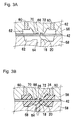
- Fig. 1 is a schematic plan view of the semiconductor device according to the first through third embodiments of the present invention.
- Fig. 2A is a schematic perspective sectional view of the semiconductor device of the first embodiment taken along lines A-A in Fig. 1.
- Fig. 2B is a partially enlarged view of a part of Fig. 2A.
- Fig. 2C is a schematic sectional view of the semiconductor device taken along lines B-B in Fig. 2A and Fig. 2B.
- Fig. 3A is a schematic sectional view showing the process of manufacturing the housing for the semiconductor device according to the first embodiment.
- Fig. 3B is a schematic sectional view showing the process of manufacturing the housing for the semiconductor device according to the first embodiment.
- FIG. 3C is a schematic sectional view showing the process of manufacturing the housing for the semiconductor device according to the first embodiment.
- Fig. 3D is a schematic sectional view showing the process of manufacturing the housing for the semiconductor device according to the first embodiment.
- Fig. 4 is a schematic perspective view of the housing for the semiconductor device according to the first embodiment.
- Fig. 5 is a schematic perspective view showing the arrangement of plurality of the housings for the semiconductor device according to the first embodiment.
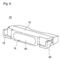
- Fig. 6 is a schematic perspective view of the semiconductor device according to the first embodiment.
- Fig. 7A is a schematic perspective sectional view of the semiconductor device of the second embodiment taken along lines A-A in Fig. 1.
- Fig. 7B is a partially enlarged view of a part of Fig. 7A.
- FIG. 7C is a schematic sectional view of the semiconductor device taken along lines C-C in Fig. 7A and Fig. 7B.
- Fig. 8A is a schematic perspective sectional view of the semiconductor device of the third embodiment taken along lines A-A in Fig. 1.
- Fig. 8B is a partially enlarged view of a part of Fig. 8A.
- Fig. 8C is a schematic sectional view of the semiconductor device taken along lines D-D in Fig. 8A and Fig. 8B.
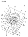
- Fig. 9A is a schematic perspective view of the semiconductor device according to the fourth embodiment.
- Fig. 9B is a schematic plan view of the semiconductor device according to the fourth embodiment.
- Fig. 9C is a schematic sectional view of the semiconductor device taken along lines E-E in Fig. 9B.
- First Embodiment Fig. 1 and Fig. 2A show a mid stage of the process of manufacturing the semiconductor device according to the first embodiment, which becomes as shown in Fig. 6 in the final state.
- the semiconductor device 10 shown in Fig. 6 is extremely thin and is used as a thin light emitting device which uses a semiconductor light emitting element as the semiconductor element 28.
- the semiconductor device 10 of the first embodiment comprises a housing 12 having a recess 14, a first lead electrode 18 and a second lead electrode 20 which are exposed on the bottom surface 16 of the recess 14.
- the first lead electrode 18 has a die bonding area 22 and a wire bonding area 24, while these areas are divided by a first wall 26 formed on the surface of the first lead electrode 18 so as to traverse the first lead electrode 18.
- the second lead electrode 20 is constituted from a wire bonding area 24' only without die bonding area.
- a second wall 34 is formed to protrude between the first lead electrode 18 and the second lead electrode 20.
- the first and second walls 26, 34 are formed integrally with the housing 12.
- the semiconductor element 28 is fixed on the substrate side thereof onto the die bonding area 22 by means of an adhesive layer 30 formed from an adhesive for die bonding, and electrodes formed on the semiconductor side are connected to the wire bonding areas 24, 24' by means of electrically conductive wires 32.
- the first and second walls 26, 34 are formed with such a height as the adhesive components of the adhesive used to form the adhesive layer 30 do not bleed from the die bonding area 22 into the wire bonding areas 24, 24' and wire bonding with the electrically conductive wires 32 is not hampered.
- the walls 26, 34 may be formed in any shape as long as the adhesive components can be prevented from bleeding phenomenon and wire bonding of the electrically conductive wires is not hampered.
- wall having such a cross section can be employed as rectangle, triangle, trapezoid, semi-circle, or semi-ellipse. It is especially preferable to form the walls 26, 34 with a triangular cross section having slopes rising from the wire bonding areas 24, 24' to the die bonding area 22 as shown in Fig. 2A which is effective in blocking the adhesive components from overflowing and makes it easier to run the electrically conductive wires 32.
- the first wall 26 extends across the first lead electrode 18 and is connected on both ends thereof to the side wall 38 of the housing 12.
- a rectangular notch 36 is formed on the edge of the first lead electrode 18 at a position where the first wall 26 is to be formed.
- the first wall 26 and the bottom portion 40 of the housing 12 are firmly connected to each other through the notch 36.
- the second wall 34 runs between the first lead electrode 18 and the second lead electrode 20 and is connected to the bottom portion 40 of the housing 12, and the second wall 34 is connected on both ends thereof to the side wall 38 of the housing 12. Therefore, the first lead electrode 18 and the second lead electrode 20 are completely separated from each other by the second wall 34.
- the die bonding area 22 where the semiconductor element 28 is mounted is surrounded by the first and second walls 26, 34 and the side walls 38, 38' of the housing 12.
- resin layer can be formed selectively only in the vicinity of the semiconductor element 28 by dripping the resin only into the surrounded die bonding area 22.
- a fluorescent material can be disposed only in the vicinity of the semiconductor light emitting element by forming a precoating layer from a translucent resin including the fluorescent material only in the die bonding area 22.
- a cross-sectional area of a connecting portion which connects the first wall 26 and the bottom portion 40 of the housing 12 is increased by forming the notch 36 in the first lead electrode 18.
- This increases the strength of the first wall 26 and improves adhesiveness between the first wall 26 and the surface of the first lead electrode 18. Improved adhesiveness is also effective in preventing the adhesive components from leaking along the interface between the first lead electrode 18 and the first wall 26 and entering the wire bonding area 24.
- the notch 36 has also an effect of making it easier to pour the molding material when forming the first wall 26.
- the first embodiment provides an advantage that it becomes easier to form the first lead electrode 18 by forming of the notch 36 in the first lead electrode 18 when providing the first lead electrode 18 which is more difficult to form than the second lead electrode 20. Also according to the first embodiment, since the semiconductor device has the first lead electrode 18 of smaller width, it is preferable to maintain the strength of the first lead electrode 18 by means of the notch 36 formed by cutting off a portion from the edge of the first lead electrode 18.
- the notch 36 is formed by cutting off a rectangular portion from the edge of the first lead electrode 18 in Fig. 2A and Fig. 2B, the notch 36 is not limited to this shape.
- the notch may be formed by cutting off in various shapes such as square, trapezoid or other tetragonal shape, polygon such as triangle or pentagon, semi-circle or semi-ellipse.
- the notch 36 shown in the drawing has such a size that is hidden behind the first wall 26, it may also be partially exposed beyond the first wall 26. Further, it may also be formed in a tapered shape which varies dimension thereof along the direction of thickness of the first lead electrode 18. In case the dimension decreases from the bottom portion 40 of the housing 12 toward the recess 14, in particular, it becomes easier to pour the molding material and maintain the strength of the first lead electrode 18.
- the semiconductor device 10 of the present invention it is preferable to fill in the recess 14 of the housing 12 with a resin so as to protect the semiconductor element 28 mounted in the recess 14 from the environment.
- a resin so as to protect the semiconductor element 28 mounted in the recess 14 from the environment.
- the semiconductor element 28 is a semiconductor light emitting element
- use of a translucent resin for filling makes it possible to extract light.
- a fluorescent material may be mixed in the translucent resin to emit light of different wavelength.
- a method for manufacturing the semiconductor device 10 of the present invention will now be described in two parts of 1. a process of manufacturing the housing 1 and 2. a process of making the semiconductor device 10 from the housing 12.
- the process of manufacturing the housing 12 will now be described with reference to Fig3.
- a metal sheet is punched through and metal plating is applied on the metal sheet thereby to make a lead frame 42.
- the lead frame 42 has a pair of the first lead electrode 18 and the second lead electrode 20 formed thereon.
- the first lead electrode 18 and the second lead electrode 20 are formed with a space kept therebetween.
- Usually a number of pairs of the lead electrodes 18, 20 are formed on one metal sheet.
- the lead frame 42 is disposed between upper and lower molds 56, 58 used in molding the housing.
- the lead frame is disposed between the upper and lower molds 56, 58, by positioning the pair of the lead electrodes 18, 20 and the hanger lead 46 of the lead frame 42 in the cavity 62 formed in the molds 56, 58 having the shape of the housing 12.
- the hanger lead 46 is a member which maintains the posture of the housing 12 which is secured on the lead frame 32, and is formed when the lead frame 42 is punched through.
- distal end of the hanger lead 46 is embedded in the side face of the housing 12 till the housing 12 is separated from the lead frame 32.
- the upper mold 56 has a protrusion 66 having the same shape as that of the recess 14 of the housing 12.
- the protrusion 66 has mold grooves 70, 72 having the same shapes as those of the walls 26, 34 formed therein.
- the molding material 68 is poured through a gate 64 of the lower mold 58 into the cavity 62 of the molds 56, 58.
- the upper mold 56 has the protrusion 66 having the same shape as that of the recess 14 of the housing 12 formed therein, so that the lead electrodes 18, 20 can be exposed in the bottom surface 16 of the recess 14 of the housing 12 without allowing the molding material 68 to deposit on the top surface of the lead electrode 18, by pouring the molding material 68 while the protrusion 66 is in contact with the top surface of the lead electrode 18.
- complete exposure is not necessarily required.
- a part of the lead electrode may also be exposed in the recess by drilling holes in the bottom surface 16 of the recess 14 while positioning the lead electrodes 18, 20 just below the bottom surface 16 of the recess 14 (namely, the lead electrodes 18, 20 are covered by the molding material of the housing).
- the semiconductor device of the present invention can be formed by establishing electrical connection between the semiconductor element and the lead electrodes through the holes.
- the molding material 68 is poured into the mold grooves 70, 72 so as to form the first wall 26 and the second wall 34. Since the mold groove 72 can be filled with the molding material 68 which is poured through the gap between the first lead electrode 18 and the second lead electrode 20, it is made easier to pour the molding material 68. In contrast, it is difficult to fill the mold groove 70 with the molding material 68. With reference made to Fig. 2C, the mold groove 70 can be filled in only by pouring the molding material 68 as indicated by arrow f 1 through a narrow gap formed between the first lead electrode 18 and the inner surface of the mold used for molding the external shape of the housing 12.
- the mold groove 72 can be filled in through the notch 36 as indicated by arrow f 2 .
- the first lead electrode 18 has the notch 36 at the position just below the first wall 26 as described above, it becomes easy to fill the mold groove 70 with the molding material 68 and such defects as the first wall 26 has missing portions due to unsatisfactory filling is less likely to occur.
- the lead frame 42 having the housing 12 shown in Fig. 1 and Fig. 4 formed on a part thereof is obtained through the series of processes shown in Fig. 3.
- the housing 12 fixed on the lead frame 42 has the first lead electrode 18 and the second lead electrode 20 exposed in the recess 14, the lead electrodes 18, 20 being connected to a first external electrode 78 and a second external electrode 80 which are connected to the lead frame 42, respectively.
- Distal ends of the hanger leads 46 are embedded in the side face of the housing 12.
- the housing 12 is held on the lead frame 42 by the external electrodes 78, 80 and the hanger leads 46.
- Fig. 1 and Fig. 4 show only one housing 12 being formed, normally a number of housings 12 (3 in column and 2 in row, 6 in all) are formed on one lead frame 42 as shown in Fig. 5.
- molds 56, 58 having a number of cavities 62 for molding the housings may be used so that all the housings 12 can be formed simultaneously by pouring the molding material into the cavities 62 simultaneously.
- the adhesive used in die bonding is selected in accordance to the purpose.
- the adhesive component may spread over the entire die bonding area 22 so as to cover the surface of the die bonding area 22.
- the first and second walls 26, 34 are formed between the die bonding area 22 and the wire bonding area 24, 24; the adhesive component does not spread up to the wire bonding area 24, 24'. Therefore, the adhesive component does not make an obstacle to the wire bonding operation carried out after die bonding.
- the walls 26, 34 are formed to such a height that does not make an obstacle to the wire bonding operation, wire bonding can be carried out by using the conventional wire bonder, and the electrically conductive wires 32 having a reasonable length can be used, thus keeping the cost of the wire bonding process comparable to that of the prior art.
- the recess 14 of the housing 12 is filled with a resin 44, so as to seal off the semiconductor element 28 and the electrically conductive wires 32.
- the resin 44 is hardened after filling in the recess 14 of the housing 12 by potting process or the like.
- a low-profile white light emitting device can be made by using a blue light emitting diode for the semiconductor light emitting element, using a translucent resin for the resin 44 and dispersing a fluorescent material which absorbs blue light and emits yellow light in the translucent resin.
- a light source suitable for a back light is obtained.
- the external electrodes 78, 80 are cut off at the position indicated with dashed line X and are separated from the lead frame 42.
- the external electrodes 78, 80 are bent along the profile of the housing 12, into the J-bend shape shown in Fig. 6 (this operation is called cut forming of the external electrodes 78, 80).
- the housing 12 is held on the lead frame 42 by the hanger leads 46 only, and it is preferable to use a fixture to hold the housing 12 so as to prevent the housing 12 from tilting and falling off the lead frame 42 due to a stress generated during the cut forming process. Since the cut forming process can be carried out simultaneously for a plurality of housings 12 formed on one lead frame 42, efficiency of manufacturing the semiconductor device 10 can be improved.
- narrow portions of the external electrodes 78, 80 are bent toward the recess 14 of the housing 12 in the early stage of the cut forming process, followed by bending into J-bend shape of the wider portion of the external electrodes 78, 80 protruding beyond the housing 12.
- cut forming may also be carried out by bending the narrow portions of the external electrodes 78, 80 in a direction opposite to the recess 14, or without bending in J-bent shape, depending on the application.
- the housing 12 When cut forming is completed, the housing 12 is removed from the lead frame 42.
- the housing 12 can be removed easily from the distal end portion of the hanger leads 46 by bending the hanger leads 46.
- the semiconductor device of the second embodiment has a V groove 50 formed on the surface of the first lead electrode 18 as shown in Fig. 7A and Fig. 7B.
- the V groove 50 is located just below the first wall 26.
- the semiconductor device 10 of the second embodiment is similar to the first embodiment except for the first lead electrode 18 and the first wall 26.
- the first wall 26 extends across the surface of the first lead electrode 18 and is bonded on both ends thereof with the side wall 38 of the housing 12.
- the V groove 50 is formed on the surface of the first lead electrode 18, and the first wall 26 is formed on the V groove 50.
- the V groove 50 is preferably formed along the first wall 26 that separates the die bonding area 22 and the wire bonding area 24. In this case, the V groove 50, together with the first wall 26, separates the surface of the first lead electrode 18 into the die bonding area 22 and the wire bonding area 24.
- V groove 50 When the V groove 50 is provided, components of the adhesive used in die bonding, even if it has leaked along the interface between the first lead electrode 18 and the first wall 26 toward the wire bonding area 24, sinks in the V groove 50 and cannot proceed further. Thus forming the V groove 50 just below the first wall 26 makes it possible to reliably prevent the adhesive component from entering the wire bonding area 24.
- the cross sectional area of the first wall 26 increases by the size of the V groove 50, strength of the first wall 26 increases.
- the increase in the cross sectional area of the first wall 26 also increases the bonding strength between the first wall 26 and the side wall 38 of the housing 12. As the bonding strength is increased, adhesiveness between the first wall 26 and the surface of the first lead electrode 18 is improved, thus effectively suppressing the adhesive components from leaking to the wire bonding area 24 along the interface between the first lead electrode 18 and the first wall 26.
- V groove 50 is advantageous also when forming the first wall 26. Further it provides an advantage when pouring the molding material 68 into the molds 56, 58 in a process corresponding to that shown in Fig. 3B. That is, when the molding material 68 is poured into the mold groove 70 of the upper mold 56 to form the first wall 26 as shown in Fig. 7C, the molding material 68 is poured through the narrow portions indicated by f 1 and f 2 in case the V groove 50 is not formed. In case the V groove 50 is formed, in contrast, the molding material 68 can be poured through wider portions indicated by arrows f 3 and f 4 thereby making it easier to fill in.
- the second embodiment is advantageous also for making it easier to form the first lead electrode 18 due to the V groove 50 formed in the first lead electrode 18, when providing the first lead electrode 18 which is more difficult to form than the second lead electrode 20.
- the V groove 50 formed in the surface of the first lead electrode 18 may be replaced with a groove having other cross sectional shape.
- cross section of the groove may have various shapes such as square, trapezoid or other tetragonal shape, polygon such as triangle or pentagon, semi-circle or semi-ellipse.
- the cross section of the V groove 50 is preferably V-shaped since it can be formed by pressing a simple tool against the surface and is more effective in preventing the intrusion of the adhesive component.
- the semiconductor device 22 where the semiconductor element 28 is disposed is surrounded by the first wall 26, the second wall 34 and the side walls 38 of the housing 12.
- resin layer can be formed selectively only in the vicinity of the semiconductor element 28 by dripping the resin only into the surrounded die bonding area 22.
- a fluorescent material can be disposed only in the vicinity of the semiconductor light emitting element by forming a precoating layer from a translucent resin including the fluorescent material only in the die bonding area 22.
- the first embodiment employs the notch 36 and the second embodiment employs the V groove 50.
- the semiconductor device of the third embodiment has both the notch 36 and the V groove 50 formed in the first lead electrode 18 as shown in Fig. 8A and Fig. 8B.
- the third embodiment is similar to the first and second embodiments. Details of the notch 36 and the V groove 50 are also similar to those of the first and second embodiments except for the points described below.
- the first wall 26 extends across the surface of the first lead electrode 18 and is bonded with the side wall 38 of the housing 12 on both ends.
- the rectangular notch 36 is formed in an edge 181 of the first lead electrode 18 at a position where the first wall 26 is to be formed. This constitution, similarly to the notch 36 of the first embodiment, achieves the effect of improving the bonding between the first wall 26 and the surface of the first lead electrode 18 and suppressing the adhesive components from bleeding phenomenon along the interface between the first lead electrode 18 and the first wall 26.
- the V groove 50 is formed in the surface of the first lead electrode 18, and the first wall 26 is formed on the V groove 50.
- the V groove 50 is preferably formed along the first wall 26 that separates the die bonding area 22 and the wire bonding area 24.
- the V groove 50, together with the first wall 26, separates the surface of the first lead electrode 18 into the die bonding area 22 and the wire bonding area 24.
- the first wall 26 is formed with small in height to such an extent that does not hamper wire bonding, and the space of the mold groove 70 is accordingly narrower. As a result, it is difficult to fill the mold groove 70 with the molding material, thus giving rise to the possibility of locally insufficient filling in case a molding material having high viscosity is used.
- forming the notch 36 widens the path of filling and makes it easier to fill in with the molding material 68. Since the molding material 68 which has passed the paths indicated by arrows f 2 and f 4 flows through the space widened by the V groove 50 and enters the mold groove 70, it becomes easier to fill than in the case where the V groove 50 is not formed.
- the notch 36 and the V groove 50 and connecting them have the advantage of making it easier to fill in to form the first wall 26, compared to the first and second embodiments.
- the portion of the first lead electrode 18 located just below the first wall 26 is made narrower due to the notch 36 and thinner due to the V groove 50, and has lower strength than the other portions of the first lead portion.
- the first lead electrode 18 bends along the V groove 50 or breaks when the distal end of the first lead electrode 18 is subjected to stress during the manufacturing process.
- the other end 502 of the V groove 50 is terminated at a position short of the edge 182 of the first lead electrode 18 so as to suppress the strength of the first lead electrode 18 from decreasing too much.
- FIG. 9A through Fig. 9C show the semiconductor device 10 of the third embodiment comprising the housing 12 having the recess 14, the first lead electrode 18 and the second lead electrode 20 which are exposed in the bottom surface 16 of the recess 14.
- the first lead electrode 18 has the die bonding area 22 and the wire bonding area 24 which are separated by the first wall 26 disposed to extend across the first lead electrode 18.
- the second lead electrode 20 is constituted from the wire bonding area 24' only without the die bonding area.
- Disposed to protrude between the first lead electrode 18 and the second lead electrode 20 is the second wall 34.
- the first and second walls 26, 34 are formed integrally with the housing 12.
- the semiconductor element 28 is fixed on the substrate side thereof onto the die bonding area 22 by means of the adhesive layer 30 formed from the adhesive for die bonding, and electrodes formed on the semiconductor side are connected to the wire bonding areas 24, 24' by means of electrically conductive wires 32.
- the semiconductor device 10 has a protective element 52 that prevents surge current from flowing into the semiconductor element 28.
- the protective element is also die-bonded onto the die bonding area 22 by means of an adhesive.
- first wall 26 and the second wall 34 are connected and are formed at the same time.
- the first and second walls 26, 34 are formed with small in height to such an extent that the adhesive component does not bleed from the die bonding area 22 to the wire bonding area 24, 24' and the wall does not hamper the wire bonding operation by means of the electrically conductive wires 32.
- the walls 26, 34 may be formed in any shape as long as the adhesive components can be prevented from bleeding phenomenon and wire bonding of the electrically conductive wires is not hampered.
- the wall may have such cross section as triangle, trapezoid, semi-circle, or semi-ellipse.
- the first wall 26 extends across the surface of the first lead electrode 18 and extends to the side wall 38 of the housing 12.
- the first lead electrode 18 has a round through hole 36' formed therein, so that the first wall 26 and the bottom portion 40 of the housing 12 are firmly connected to each other via the through hole 36'.
- the second wall 34 connects to the bottom portion 40 of the housing 12 via the space between the first lead electrode 18 and the second lead electrode 20, and the second wall 34 extends on both ends thereof to the side wall 38 of the housing 12.
- the first lead electrode 18 and the second lead electrode 20 are completely separated from each other in the recess of the housing by the second wall 34.
- the first lead electrode 18 has the through hole 36' formed at a position where the first wall 26 is to be formed. As will be seen from Fig. 9A through 9C, forming the through hole 36' causes the mid portion of the first wall 26 to be connected to the bottom portion 40 of the housing 12. This increases the strength of the first wall 26 and improved adhesiveness between the first wall 26 and the surface of the first lead electrode 18. Improved adhesiveness is also effective in preventing the adhesive components from leaking along the interface between the first lead electrode 18 and the first wall 26 and entering the wire bonding area 24.
- the notch 36 has also such effects to make it easier to pour the molding material when forming the first wall 26, and make such defect less likely to occur as the first wall 26 has defections due to unsatisfactory filling.
- the semiconductor device of the fourth embodiment has the first lead electrode 18 of larger width, strength of the first lead electrode 18 can be maintained even when the first lead electrode 18 has the through hole 36' formed to penetrate therethrough.
- the through hole 36' formed at a position other than the edge of the first lead electrode 18 is more preferable than the notch 36 formed in the edge as in the first embodiment, and functions also as the so-called anchor hole which keeps the first lead electrode 18 from lifting due to the bonding between the first wall 26 and the bottom portion 40 of the housing 12.
- the through hole 36' is formed by cutting off in round or rectangular shape in the case shown in Fig. 9A through Fig. 9C
- the through hole 36' is not limited to this shape, and may be formed by cutting of in various shapes such as square, trapezoid or other tetragonal shape, polygon such as triangle or pentagon, semi-circle or semi-ellipse.
- Diameter of the through hole 36' shown in the drawing is preferably larger than the width of the first wall 26. This is for the following reason.
- the molding material 68 poured into the through hole 36' can relatively easily flow in the longitudinal direction of the mold groove 70 but is difficult to flow in the lateral direction, when the mold groove 70 of the mold 56 is filled with the molding material 68 for forming the first wall 26.
- the molding material 68 which has entered through the through hole 36' fills the first wall 26 to the full width thereof in the early stage, and therefore the problem of unsatisfactory filling with the molding material 68 does not occur.
- diameter of the through hole 36' may be smaller than the width of the first wall 26.
- the V groove 50 may also be formed in the surface of the first lead electrode 18 as in the second embodiment.
- the groove is preferably formed along the first wall 26 just below the first wall 26. With the V groove being formed, even when the adhesive components of the adhesive for die bonding leak along the interface between the first lead electrode 18 and the first wall 26 and enter the wire bonding area, the adhesive components are stuck in the groove and cannot proceed further. Since the molding material is poured through the V groove into the space intended for the first wall 26 when forming the first wall 26, complete filling is enabled. As a result, such a defect as the first wall 26 has defections due to unsatisfactory filling is less likely to occur even when small volume and narrow pouring gate make it difficult to fill in.
- the semiconductor device 10 of the present invention it is preferable to fill in the recess 14 of the housing 12 with a resin so as to protect the semiconductor element 28 mounted in the recess 14 from the environment.
- a resin so as to protect the semiconductor element 28 mounted in the recess 14 from the environment.
- the semiconductor element 28 is a semiconductor light emitting element
- use of a translucent resin for filling makes it possible to extract light.
- a fluorescent material may be mixed in the translucent resin to emit light of different wavelength.
- the semiconductor device 10 of the fourth embodiment is considerably different from the semiconductor device 10 of the first embodiment in shape, it can be manufactured by the same manufacturing method when proper lead frame and molds are used.
- First and second lead electrodes 18, 20, first and second external electrodes 78, 80 Materials suitable for the constituent members of the semiconductor device 10 of the first through fourth embodiments will be described in detail below.
- the first lead electrode 18, the second lead electrode 20, the first external electrode 78 and the second external electrode 80 are all formed from the same electrically conductive material.
- such materials are preferably used as iron, copper, copper-clad iron, copper-clad tin, and aluminum, iron or copper plated with copper, gold or silver.
- the housing 12 and the walls 26, 34 may be formed from a thermoplastic resin such as liquid crystal polymer, polyphthalamide resin or polybutylene terephthalate (PBT).
- a semi-crystalline polymer which contains a crystal having a high melting point such as polyphthalamide resin is preferably used for the reason of high surface energy and good bonding with the sealing resin which fills the recess 14 of the housing 12.
- Use of such a material makes it less likely that the housing and the sealing resin would be parted along the interface thereof when the resin is cooled down in the process of pouring and hardening the sealing resin.
- reflectivity of the housing 12 may be increased by mixing a white pigment such as titanium oxide in the molding material.
- the adhesive layer 30 is formed from the adhesive used in die bonding, such as epoxy resin, silicone resin or other insulating adhesive, silver paste or other electrically conductive adhesive. According to the present invention, providing the wall enables it to use an adhesive which contains adhesive components having low surface tension such as epoxy resin which has been difficult to use in the prior art.
- Electrode conductive wire 32 For the electrically conductive wire 32 used in wire bonding, for example, metal wire such as gold, copper, platinum, aluminum or an alloy thereof may be used.
- resins having high weatherability can be preferably used such as silicone resin, epoxy resin, urea resin, fluororesin and hybrid resin which includes at least one of these resins.
- an inorganic material such as glass or silica gel having high light fastness may also be used. These resins and inorganic materials can be made translucent, and are therefore preferably used when manufacturing the semiconductor light emitting device 10.
- a blue light emitting diode may be used for the semiconductor element 28, using the translucent resin 44 with a fluorescent material particles dispersed therein.
- a rare earth element-based fluorescent material which absorbs blue light and emits yellow light (for example, YAG fluorescent material) is preferably used.
Abstract

Description
- The present invention relates to a semiconductor device having a semiconductor element mounted in a housing thereof, and particularly to a semiconductor light emitting device employing a semiconductor light emitting element and a semiconductor light receiving device used as photo sensor or the like.
- Semiconductor devices currently available include a semiconductor light emitting device which has a semiconductor light emitting element mounted in a housing. The housing has a recess for accommodating the semiconductor light emitting element, and exposed on the surface of the recess are a pair of lead electrodes which are connected to the electrodes of the semiconductor light emitting element. The semiconductor light emitting element is mounted in the housing by die bonding the substrate side of the semiconductor light emitting element onto one of the lead electrodes by means of a silver paste or the like, and connecting the semiconductor side of the semiconductor light emitting element to the other lead electrode by means of an electrically conductive wire.
- As the semiconductor device becomes smaller year by year, the housing also becomes smaller and accordingly the recess of the housing and the lead electrodes exposed in the recess become smaller in size. When the semiconductor element is mounted in the small housing, bleeding phenomenon, that is to say, flowing the silver paste for die bonding from the one lead electrode to the other lead electrode is likely to occur, eventually causing short circuiting of the semiconductor device. It is known to prevent the bleeding phenomenon by providing a protrusion between the lead electrodes (refer to, for example, Japanese Unexamined Patent Publication (Kokai)
No. 10-294495 No. 62-47156 - In a light emitting device comprising an LED chip and a protective element (Zener diode) in such a constitution as the protective element is die bonded on a negative lead electrode and the LED chip is wire bonded on the same negative lead electrode, a first bonding region where die bonding is carried out and a second bonding region where wire bonding is carried out are separated from each other by a wall (refer to, for example, Japanese Unexamined Patent Publication (Kokai) No. 2005-33194). The wall prevents the die bonding material for die bonding of the protective element from flowing into the second bonding region.
- In a semiconductor light emitting element employing nitride semiconductor, the semiconductor element is formed on an insulating substrate such as sapphire, which disables electrical continuity to be established through the substrate. For this reason, both a positive electrode and a negative electrode of the semiconductor light emitting element are formed on the semiconductor side, and are wire bonded to the corresponding lead electrodes when mounting the element. At this time, the semiconductor light emitting element is bonded onto either of the lead electrodes by means of an electrically conductive adhesive such as silver paste or an insulating adhesive such as die bonding resin.
- In case an adhesive including a liquid component such as plasticizer of low surface tension is used when die bonding the semiconductor light emitting element, the liquid component of the adhesive and the adhesive itself (these will be collectively referred to as adhesive components) can easily spread over the surface of the lead electrode (which is also bleeding phenomenon) so as to cover the surface of the lead electrode, even when application of the adhesive is limited to the die bonding area of the lead electrode. Particularly when both die bonding and wire bonding are carried out in the same lead electrode, the die bonding area and the wire bonding area are disposed adjacent to each other on the same surface of the same lead electrode, and therefore the adhesive components can very easily overflow. Bleeding phenomenon can occur far more easily in this case than in the prior art in which the lead electrodes are disposed apart from each other. If the lead electrode is covered by the adhesive components after die bonding, the electrically conductive wire connecting the lead electrode and the electrode of the semiconductor light emitting element cannot be fixed sufficiently on the lead electrode when wire bonding, and it becomes impossible to establish electrical continuity by means of the electrically conductive wire in case an insulating adhesive is used.
- The constitutions described in Japanese Unexamined Patent Publication (Kokai)
No. 10-294495 No. 62-471562
It may seem that this problem could be solved by providing the wall on the surface of the lead electrode as disclosed inJapanese Unexamined Patent Publication (Kokai) No. 2005-33194 - However, with the light emitting devices of these days which have become extremely small and thin, new problems that cannot be solved by the technology of
Japanese Unexamined Patent Publication (Kokai) No. 2005-33194
First, since the wall is limited to small dimensions in width and height, sufficient quantity of a material to form the wall may not be put into a mold groove which is provided with a mold in order to mold the wall. Particularly when the molding material has a high viscosity, the mold groove may not be filled satisfactorily with the molding material thus resulting in the wall having defections.
Second, adhesiveness between the wall and the lead electrode can be weak, thus giving rise to the possibility of leak of the adhesive components along the interface thereof. This can cause significant influence particularly when the adhesive component has low surface tension. - With the background described above, an object of the present invention is to provide a semiconductor device wherein the adhesive components do not overflow nor leak to the wire bonding area even when an adhesive consisting of adhesive components having low surface tension is used in the adhesive layer for die bonding, and the overflow and leak preventing function can be maintained satisfactorily even when the device is made smaller and thinner.
- First aspect of the present invention is a semiconductor device comprising a semiconductor element having a pair of electrodes, a housing having a recess for accommodating the semiconductor element, a first lead electrode and a second lead electrode which are exposed on the bottom of the recess, an adhesive layer for die bonding between the semiconductor element and the first lead electrode, and electrically conductive wires for wire bonding between one electrode of the pair of electrodes of the semiconductor element and the first lead electrode and between the other electrode and the second lead electrode, wherein the housing has at least one wall formed to extend across the bottom surface of the recess so as to divide the surface of the first lead electrode into a die bonding area and a wire bonding area, and the first lead electrode has a cut-out portion which is formed by cutting off a portion of an edge of the lead electrode and located at least just below the wall, while the wall and the bottom portion of the housing are connected to each other through the cut-out portion.
- According to the first aspect of the present invention, since the cut-out portion is formed just below the first wall, the first wall and the housing can be connected through the cut-out portion, and therefore a cross-sectional area of a connecting portion between them are increased. This enables it to improve adhesiveness between the first wall and the surface of the first lead electrode. The improved adhesiveness is effective in preventing the adhesive components from leaking to the wire bonding area along the interface between the first lead electrode and the first wall.
The cut-out portion has also an effect of making the first wall easier to pour the molding material when forming it. The passage through which the molding material flows into the first wall is widened by the cut-out portion. The first wall is small in height to such an extent that does not hamper wire bonding, and therefore it is difficult to fill in the molding material which may result in locally insufficient filling in case the molding material has high viscosity. However, forming the cut-out portion widens the passage for filling and makes it easier to fill in with the molding material.
According to the present invention, the cut-out portion may have a form of notch formed by cutting off a portion of the edge of the first lead electrode, or a form of through hole formed in the first lead electrode. - Second aspect of the present invention is a semiconductor device comprising a semiconductor element having a pair of electrodes, a housing having a recess for accommodating the semiconductor element, a first lead electrode and a second lead electrode which are exposed on the bottom surface of the recess, an adhesive layer for die bonding between the semiconductor element and the first lead electrode, and electrically conductive wires for wire bonding between one electrode of the pair of electrodes of the semiconductor element and the first lead electrode and between the other electrode and the second lead electrode, wherein the housing has at least one wall formed to extend across the bottom surface of the recess so as to divide the surface of the first lead electrode into a die bonding area and a wire bonding area, and the first lead electrode has a groove which is formed in the surface thereof so as to extend along the wall and located at least just below the wall, while the bottom of the wall is engaged with the groove.
- According to the second aspect of the present invention, the groove is formed in the surface of the first lead electrode, and the first wall is formed on the groove. Since the groove is formed along the first wall which separates the die bonding area and the wire bonding area, even if the adhesive components of the adhesive for die bonding tend to leak form the die bond area to the wire bonding area along the interface between the first lead electrode and the first wall, the adhesive components are stuck in the groove and cannot proceed further. Thus the groove formed just below the first wall enables it to surely prevent the adhesive component from entering the wire bonding area. Also as the cross section of the first wall is increased by the groove, bonding strength between the first wall and the side wall of the housing is also increased. As the bonding strength is increased, adhesiveness between the first wall and the surface of the first lead electrode can be improved, which is effective in preventing the adhesive components from leaking to the wire bonding area along the interface between the first lead electrode and the first wall.
- Furthermore, the second aspect of the present invention is advantageous also when forming the first wall. The groove leads to larger opening for pouring the molding material, which makes it easier to fill in and therefore prevents defections of the first wall formed by insufficient filling in the first wall with the molding material.
The first wall is small in height to such an extent that does not hamper wire bonding, and therefore it is difficult to fill in the molding material which may result in locally insufficient filling in case the molding material has high viscosity. However, forming the groove widens the passage for filling and makes it easier to fill with the molding material. - In the semiconductor device of the present invention, the adhesive components do not overflow nor leak to the wire bonding area even when an adhesive consisting of adhesive components having low surface tension is used in the adhesive layer for die bonding, and the overflow and leak preventing function can be maintained satisfactorily even when the device is made smaller and thinner.
- Fig. 1 is a schematic plan view of the semiconductor device according to the first through third embodiments of the present invention.
Fig. 2A is a schematic perspective sectional view of the semiconductor device of the first embodiment taken along lines A-A in Fig. 1.
Fig. 2B is a partially enlarged view of a part of Fig. 2A.
Fig. 2C is a schematic sectional view of the semiconductor device taken along lines B-B in Fig. 2A and Fig. 2B.
Fig. 3A is a schematic sectional view showing the process of manufacturing the housing for the semiconductor device according to the first embodiment.
Fig. 3B is a schematic sectional view showing the process of manufacturing the housing for the semiconductor device according to the first embodiment.
Fig. 3C is a schematic sectional view showing the process of manufacturing the housing for the semiconductor device according to the first embodiment.
Fig. 3D is a schematic sectional view showing the process of manufacturing the housing for the semiconductor device according to the first embodiment.
Fig. 4 is a schematic perspective view of the housing for the semiconductor device according to the first embodiment.
Fig. 5 is a schematic perspective view showing the arrangement of plurality of the housings for the semiconductor device according to the first embodiment.
Fig. 6 is a schematic perspective view of the semiconductor device according to the first embodiment.
Fig. 7A is a schematic perspective sectional view of the semiconductor device of the second embodiment taken along lines A-A in Fig. 1.
Fig. 7B is a partially enlarged view of a part of Fig. 7A.
Fig. 7C is a schematic sectional view of the semiconductor device taken along lines C-C in Fig. 7A and Fig. 7B.
Fig. 8A is a schematic perspective sectional view of the semiconductor device of the third embodiment taken along lines A-A in Fig. 1.
Fig. 8B is a partially enlarged view of a part of Fig. 8A.
Fig. 8C is a schematic sectional view of the semiconductor device taken along lines D-D in Fig. 8A and Fig. 8B.
Fig. 9A is a schematic perspective view of the semiconductor device according to the fourth embodiment.
Fig. 9B is a schematic plan view of the semiconductor device according to the fourth embodiment.
Fig. 9C is a schematic sectional view of the semiconductor device taken along lines E-E in Fig. 9B. -
- 10
- Semiconductor light emitting device
- 12
- Housing
- 14
- Recess
- 18
- First lead electrode
- 20
- Second lead electrode
- 22
- Die bonding area
- 24, 24'
- Wire bonding area
- 26
- First wall
- 28
- Semiconductor element
- 30
- Adhesive layer
- 32
- Electrically conductive wire
- 34
- Second wall
- 36
- Notch
- 36'
- Through hole
- 42
- Lead frame
- 50
- V groove
- 52
- Protective element
- 78
- First external electrode
- 80
- Second external electrode
- 181, 182
- Edge of first lead electrode
- 501
- One end of V groove
- 502
- Other end of V groove
- First Embodiment
Fig. 1 and Fig. 2A show a mid stage of the process of manufacturing the semiconductor device according to the first embodiment, which becomes as shown in Fig. 6 in the final state. Thesemiconductor device 10 shown in Fig. 6 is extremely thin and is used as a thin light emitting device which uses a semiconductor light emitting element as thesemiconductor element 28.
Thesemiconductor device 10 of the first embodiment comprises ahousing 12 having arecess 14, afirst lead electrode 18 and asecond lead electrode 20 which are exposed on thebottom surface 16 of therecess 14. Thefirst lead electrode 18 has adie bonding area 22 and awire bonding area 24, while these areas are divided by afirst wall 26 formed on the surface of thefirst lead electrode 18 so as to traverse thefirst lead electrode 18. Thesecond lead electrode 20 is constituted from a wire bonding area 24' only without die bonding area. Asecond wall 34 is formed to protrude between thefirst lead electrode 18 and thesecond lead electrode 20. The first andsecond walls housing 12. Thesemiconductor element 28 is fixed on the substrate side thereof onto thedie bonding area 22 by means of anadhesive layer 30 formed from an adhesive for die bonding, and electrodes formed on the semiconductor side are connected to thewire bonding areas 24, 24' by means of electricallyconductive wires 32. - The first and
second walls adhesive layer 30 do not bleed from thedie bonding area 22 into thewire bonding areas 24, 24' and wire bonding with the electricallyconductive wires 32 is not hampered. Thewalls walls wire bonding areas 24, 24' to thedie bonding area 22 as shown in Fig. 2A which is effective in blocking the adhesive components from overflowing and makes it easier to run the electricallyconductive wires 32. - As shown in Fig. 1 and Figs.2A through 2C, the
first wall 26 extends across thefirst lead electrode 18 and is connected on both ends thereof to theside wall 38 of thehousing 12. In the first embodiment, arectangular notch 36 is formed on the edge of thefirst lead electrode 18 at a position where thefirst wall 26 is to be formed. Thefirst wall 26 and thebottom portion 40 of thehousing 12 are firmly connected to each other through thenotch 36. By forming thenotch 36, adhesiveness between thefirst wall 26 and the surface of thefirst lead electrode 18 is improved, and bleeding phenomenon of the adhesive components along the interface between thefirst lead electrode 18 and thefirst wall 26 can be suppressed more effectively.
Thesecond wall 34 runs between thefirst lead electrode 18 and thesecond lead electrode 20 and is connected to thebottom portion 40 of thehousing 12, and thesecond wall 34 is connected on both ends thereof to theside wall 38 of thehousing 12. Therefore, thefirst lead electrode 18 and thesecond lead electrode 20 are completely separated from each other by thesecond wall 34. - In the
semiconductor device 10 shown in Fig. 1 and Fig. 2A, thedie bonding area 22 where thesemiconductor element 28 is mounted is surrounded by the first andsecond walls side walls 38, 38' of thehousing 12. In thissemiconductor device 10, resin layer can be formed selectively only in the vicinity of thesemiconductor element 28 by dripping the resin only into the surroundeddie bonding area 22. In case the semiconductor light emitting element is used as thesemiconductor element 28, for example, a fluorescent material can be disposed only in the vicinity of the semiconductor light emitting element by forming a precoating layer from a translucent resin including the fluorescent material only in thedie bonding area 22. - As will be seen from Fig. 2B and Fig. 2C, a cross-sectional area of a connecting portion which connects the
first wall 26 and thebottom portion 40 of thehousing 12 is increased by forming thenotch 36 in thefirst lead electrode 18. This increases the strength of thefirst wall 26 and improves adhesiveness between thefirst wall 26 and the surface of thefirst lead electrode 18. Improved adhesiveness is also effective in preventing the adhesive components from leaking along the interface between thefirst lead electrode 18 and thefirst wall 26 and entering thewire bonding area 24.
Thenotch 36 has also an effect of making it easier to pour the molding material when forming thefirst wall 26. Arrow f1 (on left side in drawing) and arrow f2 (on right side in drawing) in Fig. 2C indicate the paths along which the molding material flows into thefirst wall 26, and the passage indicated by arrow f2 is made wider than that indicated by arrow f1 due to the presence of thenotch 36. Thefirst wall 26 is formed with lower height to such an extent that does not hamper wire bonding, and it is difficult to fill in the molding material which may result in locally insufficient filling in case a molding material having high viscosity is used. However, forming thenotch 36 widens the passage for filling and makes it easier to fill with the molding material. Thus the first embodiment provides an advantage that it becomes easier to form thefirst lead electrode 18 by forming of thenotch 36 in thefirst lead electrode 18 when providing thefirst lead electrode 18 which is more difficult to form than thesecond lead electrode 20.
Also according to the first embodiment, since the semiconductor device has thefirst lead electrode 18 of smaller width, it is preferable to maintain the strength of thefirst lead electrode 18 by means of thenotch 36 formed by cutting off a portion from the edge of thefirst lead electrode 18. - While the
notch 36 is formed by cutting off a rectangular portion from the edge of thefirst lead electrode 18 in Fig. 2A and Fig. 2B, thenotch 36 is not limited to this shape. For example, the notch may be formed by cutting off in various shapes such as square, trapezoid or other tetragonal shape, polygon such as triangle or pentagon, semi-circle or semi-ellipse. While thenotch 36 shown in the drawing has such a size that is hidden behind thefirst wall 26, it may also be partially exposed beyond thefirst wall 26. Further, it may also be formed in a tapered shape which varies dimension thereof along the direction of thickness of thefirst lead electrode 18. In case the dimension decreases from thebottom portion 40 of thehousing 12 toward therecess 14, in particular, it becomes easier to pour the molding material and maintain the strength of thefirst lead electrode 18. - In the
semiconductor device 10 of the present invention, it is preferable to fill in therecess 14 of thehousing 12 with a resin so as to protect thesemiconductor element 28 mounted in therecess 14 from the environment. Particularly in case thesemiconductor element 28 is a semiconductor light emitting element, use of a translucent resin for filling makes it possible to extract light. When it is desired to produce light of a color different from that of light from the semiconductorlight emitting element 28, a fluorescent material may be mixed in the translucent resin to emit light of different wavelength. - A method for manufacturing the
semiconductor device 10 of the present invention will now be described in two parts of 1. a process of manufacturing the housing 1 and 2. a process of making thesemiconductor device 10 from thehousing 12. - (1. Manufacturing of housing 12)
The process of manufacturing thehousing 12 will now be described with reference to Fig3.
First, a metal sheet is punched through and metal plating is applied on the metal sheet thereby to make alead frame 42. Thelead frame 42 has a pair of thefirst lead electrode 18 and thesecond lead electrode 20 formed thereon. Thefirst lead electrode 18 and thesecond lead electrode 20 are formed with a space kept therebetween. Usually a number of pairs of thelead electrodes - As shown in Fig. 3A, the
lead frame 42 is disposed between upper andlower molds lower molds lead electrodes hanger lead 46 of thelead frame 42 in thecavity 62 formed in themolds housing 12. Thehanger lead 46 is a member which maintains the posture of thehousing 12 which is secured on thelead frame 32, and is formed when thelead frame 42 is punched through. As shown in Fig. 1, distal end of thehanger lead 46 is embedded in the side face of thehousing 12 till thehousing 12 is separated from thelead frame 32.
Theupper mold 56 has aprotrusion 66 having the same shape as that of therecess 14 of thehousing 12. Theprotrusion 66 hasmold grooves walls - Then as shown in Fig. 3B, the
molding material 68 is poured through agate 64 of thelower mold 58 into thecavity 62 of themolds upper mold 56 has theprotrusion 66 having the same shape as that of therecess 14 of thehousing 12 formed therein, so that thelead electrodes bottom surface 16 of therecess 14 of thehousing 12 without allowing themolding material 68 to deposit on the top surface of thelead electrode 18, by pouring themolding material 68 while theprotrusion 66 is in contact with the top surface of thelead electrode 18.
In this example, while thelead electrode 18 is completely exposed in thebottom surface 16 of therecess 14 of thehousing 12, complete exposure is not necessarily required. For example, a part of the lead electrode may also be exposed in the recess by drilling holes in thebottom surface 16 of therecess 14 while positioning thelead electrodes bottom surface 16 of the recess 14 (namely, thelead electrodes - The
molding material 68 is poured into themold grooves first wall 26 and thesecond wall 34. Since themold groove 72 can be filled with themolding material 68 which is poured through the gap between thefirst lead electrode 18 and thesecond lead electrode 20, it is made easier to pour themolding material 68. In contrast, it is difficult to fill themold groove 70 with themolding material 68. With reference made to Fig. 2C, themold groove 70 can be filled in only by pouring themolding material 68 as indicated by arrow f1 through a narrow gap formed between thefirst lead electrode 18 and the inner surface of the mold used for molding the external shape of thehousing 12. However, it is made easier to pour themolding material 68 by providing thenotch 36 in thefirst lead electrode 18 as in the first embodiment, since themold groove 72 can be filled in through thenotch 36 as indicated by arrow f2. When thefirst lead electrode 18 has thenotch 36 at the position just below thefirst wall 26 as described above, it becomes easy to fill themold groove 70 with themolding material 68 and such defects as thefirst wall 26 has missing portions due to unsatisfactory filling is less likely to occur. - When the
cavity 62 and themold grooves molds molding material 68 as shown in Fig. 3C, pouring of themolding material 68 is stopped and themolding material 68 is hardened.
When themolding material 68 has fully hardened, thelower mold 58 is removed first, then theupper mold 56 is removed so as to take out thehousing 12. When theupper mold 56 is removed, such troubles tend to occur as thelead frame 42 is distorted or thehousing 12 tilts. Thehousing 12 can be taken out without causing such troubles, for example, by pressing anejector pin 60, which is inserted slidably to penetrate through theupper mold 56, in the direction indicated by the arrow. - The
lead frame 42 having thehousing 12 shown in Fig. 1 and Fig. 4 formed on a part thereof is obtained through the series of processes shown in Fig. 3.
As shown in Fig. 1, thehousing 12 fixed on thelead frame 42 has thefirst lead electrode 18 and thesecond lead electrode 20 exposed in therecess 14, thelead electrodes external electrode 78 and a secondexternal electrode 80 which are connected to thelead frame 42, respectively. Distal ends of the hanger leads 46 are embedded in the side face of thehousing 12. Thehousing 12 is held on thelead frame 42 by theexternal electrodes - While Fig. 1 and Fig. 4 show only one
housing 12 being formed, normally a number of housings 12 (3 in column and 2 in row, 6 in all) are formed on onelead frame 42 as shown in Fig. 5. In case a number ofhousings 12 are formed,molds cavities 62 for molding the housings may be used so that all thehousings 12 can be formed simultaneously by pouring the molding material into thecavities 62 simultaneously. - (2. Process of manufacturing semiconductor device 10)
The process of manufacturing thesemiconductor device 10 by mounting thesemiconductor element 28 on thehousing 12 will now be described with reference to Fig. 1 and Fig. 4.
Thesemiconductor element 28 is die-bonded onto thedie bonding area 22 of thefirst lead electrode 18 within therecess 14 of thehousing 12, then the electrodes (positive electrode and negative electrode) of thesemiconductor element 28 are connected to thewire bonding area 24 of thefirst lead electrode 18 and the lead electrode 20 (which is also a wire bonding area 24'), respectively, by wire boding using the electricallyconductive wires 32. - The adhesive used in die bonding is selected in accordance to the purpose. When an adhesive having low surface tension is used, for example, the adhesive component may spread over the entire
die bonding area 22 so as to cover the surface of thedie bonding area 22. However, since the first andsecond walls die bonding area 22 and thewire bonding area wire bonding area 24, 24'. Therefore, the adhesive component does not make an obstacle to the wire bonding operation carried out after die bonding.
Also because thewalls conductive wires 32 having a reasonable length can be used, thus keeping the cost of the wire bonding process comparable to that of the prior art. - Then the
recess 14 of thehousing 12 is filled with aresin 44, so as to seal off thesemiconductor element 28 and the electricallyconductive wires 32. Theresin 44 is hardened after filling in therecess 14 of thehousing 12 by potting process or the like.
Then a low-profile white light emitting device can be made by using a blue light emitting diode for the semiconductor light emitting element, using a translucent resin for theresin 44 and dispersing a fluorescent material which absorbs blue light and emits yellow light in the translucent resin. When this low-profile white light emitting device is combined with an optical guide, a light source suitable for a back light is obtained. - When sealing with the
resin 44 is completed, theexternal electrodes lead frame 42. Theexternal electrodes housing 12, into the J-bend shape shown in Fig. 6 (this operation is called cut forming of theexternal electrodes 78, 80). Under this condition, thehousing 12 is held on thelead frame 42 by the hanger leads 46 only, and it is preferable to use a fixture to hold thehousing 12 so as to prevent thehousing 12 from tilting and falling off thelead frame 42 due to a stress generated during the cut forming process.
Since the cut forming process can be carried out simultaneously for a plurality ofhousings 12 formed on onelead frame 42, efficiency of manufacturing thesemiconductor device 10 can be improved. - When the
semiconductor device 10 shown in Fig. 6 is manufactured, narrow portions of theexternal electrodes recess 14 of thehousing 12 in the early stage of the cut forming process, followed by bending into J-bend shape of the wider portion of theexternal electrodes housing 12. Besides this, cut forming may also be carried out by bending the narrow portions of theexternal electrodes recess 14, or without bending in J-bent shape, depending on the application. - When cut forming is completed, the
housing 12 is removed from thelead frame 42. Thehousing 12 can be removed easily from the distal end portion of the hanger leads 46 by bending the hanger leads 46. - Second Embodiment
The semiconductor device of the second embodiment has aV groove 50 formed on the surface of thefirst lead electrode 18 as shown in Fig. 7A and Fig. 7B. TheV groove 50 is located just below thefirst wall 26. Thesemiconductor device 10 of the second embodiment is similar to the first embodiment except for thefirst lead electrode 18 and thefirst wall 26. - As shown in Fig. 7A through Fig. 7C, the
first wall 26 extends across the surface of thefirst lead electrode 18 and is bonded on both ends thereof with theside wall 38 of thehousing 12. In the second embodiment, theV groove 50 is formed on the surface of thefirst lead electrode 18, and thefirst wall 26 is formed on theV groove 50. TheV groove 50 is preferably formed along thefirst wall 26 that separates thedie bonding area 22 and thewire bonding area 24. In this case, theV groove 50, together with thefirst wall 26, separates the surface of thefirst lead electrode 18 into thedie bonding area 22 and thewire bonding area 24. When theV groove 50 is provided, components of the adhesive used in die bonding, even if it has leaked along the interface between thefirst lead electrode 18 and thefirst wall 26 toward thewire bonding area 24, sinks in theV groove 50 and cannot proceed further. Thus forming theV groove 50 just below thefirst wall 26 makes it possible to reliably prevent the adhesive component from entering thewire bonding area 24. - As the cross sectional area of the
first wall 26 increases by the size of theV groove 50, strength of thefirst wall 26 increases. The increase in the cross sectional area of thefirst wall 26 also increases the bonding strength between thefirst wall 26 and theside wall 38 of thehousing 12. As the bonding strength is increased, adhesiveness between thefirst wall 26 and the surface of thefirst lead electrode 18 is improved, thus effectively suppressing the adhesive components from leaking to thewire bonding area 24 along the interface between thefirst lead electrode 18 and thefirst wall 26. - Existence of the
V groove 50 is advantageous also when forming thefirst wall 26. Further it provides an advantage when pouring themolding material 68 into themolds molding material 68 is poured into themold groove 70 of theupper mold 56 to form thefirst wall 26 as shown in Fig. 7C, themolding material 68 is poured through the narrow portions indicated by f1 and f2 in case theV groove 50 is not formed. In case theV groove 50 is formed, in contrast, themolding material 68 can be poured through wider portions indicated by arrows f3 and f4 thereby making it easier to fill in. Thus in case thefirst lead electrode 18 has theV groove 50 formed just below thefirst wall 26, it becomes easier to fill themold groove 70 with themolding material 68, and such defect as thefirst wall 26 has missing portions due to unsatisfactory filling is less likely to occur. In this way, the second embodiment is advantageous also for making it easier to form thefirst lead electrode 18 due to theV groove 50 formed in thefirst lead electrode 18, when providing thefirst lead electrode 18 which is more difficult to form than thesecond lead electrode 20. - The
V groove 50 formed in the surface of thefirst lead electrode 18 may be replaced with a groove having other cross sectional shape. For example, cross section of the groove may have various shapes such as square, trapezoid or other tetragonal shape, polygon such as triangle or pentagon, semi-circle or semi-ellipse. The cross section of theV groove 50 is preferably V-shaped since it can be formed by pressing a simple tool against the surface and is more effective in preventing the intrusion of the adhesive component. - In the
semiconductor device 10 shown in Fig. 7A, thesemiconductor device 22 where thesemiconductor element 28 is disposed is surrounded by thefirst wall 26, thesecond wall 34 and theside walls 38 of thehousing 12. In thissemiconductor device 10, resin layer can be formed selectively only in the vicinity of thesemiconductor element 28 by dripping the resin only into the surroundeddie bonding area 22. In case the semiconductor light emitting element is used as thesemiconductor element 28, for example, a fluorescent material can be disposed only in the vicinity of the semiconductor light emitting element by forming a precoating layer from a translucent resin including the fluorescent material only in thedie bonding area 22. - Third Embodiment
The first embodiment employs thenotch 36 and the second embodiment employs theV groove 50. The semiconductor device of the third embodiment has both thenotch 36 and theV groove 50 formed in thefirst lead electrode 18 as shown in Fig. 8A and Fig. 8B. With other respects, the third embodiment is similar to the first and second embodiments. Details of thenotch 36 and theV groove 50 are also similar to those of the first and second embodiments except for the points described below. - As shown in Fig. 8A through Fig. 8C, the
first wall 26 extends across the surface of thefirst lead electrode 18 and is bonded with theside wall 38 of thehousing 12 on both ends.
In the third embodiment, therectangular notch 36 is formed in anedge 181 of thefirst lead electrode 18 at a position where thefirst wall 26 is to be formed. This constitution, similarly to thenotch 36 of the first embodiment, achieves the effect of improving the bonding between thefirst wall 26 and the surface of thefirst lead electrode 18 and suppressing the adhesive components from bleeding phenomenon along the interface between thefirst lead electrode 18 and thefirst wall 26. - In the third embodiment, the
V groove 50 is formed in the surface of thefirst lead electrode 18, and thefirst wall 26 is formed on theV groove 50. TheV groove 50 is preferably formed along thefirst wall 26 that separates thedie bonding area 22 and thewire bonding area 24. In this case, theV groove 50, together with thefirst wall 26, separates the surface of thefirst lead electrode 18 into thedie bonding area 22 and thewire bonding area 24. Thus forming theV groove 50 just below thefirst wall 26 makes it possible to reliably prevent the adhesive component from entering thewire bonding area 24. - According to the third embodiment, since one
end 501 of theV groove 50 is connected to thenotch 36, it is very advantageous when pouring themolding material 68 into themolds
Arrow f1 (on left side in drawing) and arrows f2 and f4 (on right side in drawing) in Fig. 8C indicate the paths along which themolding material 68 flows into themold groove 70 of themold 56 for forming thefirst wall 26. The paths indicated by arrows f2 and f4 are made wider than that indicated by arrow f1 due to the presence of thenotch 36. Thefirst wall 26 is formed with small in height to such an extent that does not hamper wire bonding, and the space of themold groove 70 is accordingly narrower. As a result, it is difficult to fill themold groove 70 with the molding material, thus giving rise to the possibility of locally insufficient filling in case a molding material having high viscosity is used. However, forming thenotch 36 widens the path of filling and makes it easier to fill in with themolding material 68.
Since themolding material 68 which has passed the paths indicated by arrows f2 and f4 flows through the space widened by theV groove 50 and enters themold groove 70, it becomes easier to fill than in the case where theV groove 50 is not formed. - As described above, providing the
notch 36 and theV groove 50 and connecting them have the advantage of making it easier to fill in to form thefirst wall 26, compared to the first and second embodiments.
On the other hand, the portion of thefirst lead electrode 18 located just below thefirst wall 26 is made narrower due to thenotch 36 and thinner due to theV groove 50, and has lower strength than the other portions of the first lead portion. There is also a possibility that thefirst lead electrode 18 bends along theV groove 50 or breaks when the distal end of thefirst lead electrode 18 is subjected to stress during the manufacturing process.
For this reason, in the third embodiment, theother end 502 of theV groove 50 is terminated at a position short of theedge 182 of thefirst lead electrode 18 so as to suppress the strength of thefirst lead electrode 18 from decreasing too much. However, it is more desirable from the view point of filling with themolding material 68, that theother end 502 of theV groove 50 reaches theedge 182 of thefirst lead electrode 18. Therefore, it is preferable to extend theother end 502 to theedge 182 in case thefirst lead electrode 18 is strong enough and there is no possibility of bending or breaking. - Fourth Embodiment
Fig. 9A through Fig. 9C show thesemiconductor device 10 of the third embodiment comprising thehousing 12 having therecess 14, thefirst lead electrode 18 and thesecond lead electrode 20 which are exposed in thebottom surface 16 of therecess 14. Thefirst lead electrode 18 has thedie bonding area 22 and thewire bonding area 24 which are separated by thefirst wall 26 disposed to extend across thefirst lead electrode 18. Thesecond lead electrode 20 is constituted from the wire bonding area 24' only without the die bonding area. Disposed to protrude between thefirst lead electrode 18 and thesecond lead electrode 20 is thesecond wall 34. The first andsecond walls housing 12. Thesemiconductor element 28 is fixed on the substrate side thereof onto thedie bonding area 22 by means of theadhesive layer 30 formed from the adhesive for die bonding, and electrodes formed on the semiconductor side are connected to thewire bonding areas 24, 24' by means of electricallyconductive wires 32. Thesemiconductor device 10 has aprotective element 52 that prevents surge current from flowing into thesemiconductor element 28. The protective element is also die-bonded onto thedie bonding area 22 by means of an adhesive. - In the fourth embodiment, the
first wall 26 and thesecond wall 34 are connected and are formed at the same time. The first andsecond walls die bonding area 22 to thewire bonding area 24, 24' and the wall does not hamper the wire bonding operation by means of the electricallyconductive wires 32. Thewalls - As shown in Fig. 9A through 9C, the
first wall 26 extends across the surface of thefirst lead electrode 18 and extends to theside wall 38 of thehousing 12. In the fourth embodiment, thefirst lead electrode 18 has a round through hole 36' formed therein, so that thefirst wall 26 and thebottom portion 40 of thehousing 12 are firmly connected to each other via the through hole 36'. By forming the through hole 36', adhesiveness between thefirst wall 26 and the surface of thefirst lead electrode 18 can be improved, and bleeding phenomenon of the bonding resin along the interface between thefirst lead electrode 18 and thefirst wall 26 can be suppressed more effectively.
Thesecond wall 34 connects to thebottom portion 40 of thehousing 12 via the space between thefirst lead electrode 18 and thesecond lead electrode 20, and thesecond wall 34 extends on both ends thereof to theside wall 38 of thehousing 12. Thus thefirst lead electrode 18 and thesecond lead electrode 20 are completely separated from each other in the recess of the housing by thesecond wall 34. - The
first lead electrode 18 has the through hole 36' formed at a position where thefirst wall 26 is to be formed. As will be seen from Fig. 9A through 9C, forming the through hole 36' causes the mid portion of thefirst wall 26 to be connected to thebottom portion 40 of thehousing 12. This increases the strength of thefirst wall 26 and improved adhesiveness between thefirst wall 26 and the surface of thefirst lead electrode 18. Improved adhesiveness is also effective in preventing the adhesive components from leaking along the interface between thefirst lead electrode 18 and thefirst wall 26 and entering thewire bonding area 24. Thenotch 36 has also such effects to make it easier to pour the molding material when forming thefirst wall 26, and make such defect less likely to occur as thefirst wall 26 has defections due to unsatisfactory filling. - Since the semiconductor device of the fourth embodiment has the
first lead electrode 18 of larger width, strength of thefirst lead electrode 18 can be maintained even when thefirst lead electrode 18 has the through hole 36' formed to penetrate therethrough. In the case of thefirst lead electrode 18 of larger width, the through hole 36' formed at a position other than the edge of thefirst lead electrode 18 is more preferable than thenotch 36 formed in the edge as in the first embodiment, and functions also as the so-called anchor hole which keeps thefirst lead electrode 18 from lifting due to the bonding between thefirst wall 26 and thebottom portion 40 of thehousing 12. - While the through hole 36' is formed by cutting off in round or rectangular shape in the case shown in Fig. 9A through Fig. 9C, the through hole 36' is not limited to this shape, and may be formed by cutting of in various shapes such as square, trapezoid or other tetragonal shape, polygon such as triangle or pentagon, semi-circle or semi-ellipse. Diameter of the through hole 36' shown in the drawing is preferably larger than the width of the
first wall 26. This is for the following reason.
Themolding material 68 poured into the through hole 36' can relatively easily flow in the longitudinal direction of themold groove 70 but is difficult to flow in the lateral direction, when themold groove 70 of themold 56 is filled with themolding material 68 for forming thefirst wall 26. Difficulty of flowing becomes more remarkable when height of themold groove 70 becomes smaller. In the present invention, since height of thefirst wall 26 is made small to such an extent that does not hamper wire bonding with the electricallyconductive wire 32, it is very difficult for themolding material 68 which has entered through the through hole 36' to flow in the direction of width of themold groove 70. As a result, such defect may occur as thefirst wall 26 has defections due to unsatisfactory filling in the lateral direction of thefirst wall 26 in the vicinity of the through hole 36'. However, when the through hole 36' is formed with a diameter larger than the width of thefirst wall 26, themolding material 68 which has entered through the through hole 36' fills thefirst wall 26 to the full width thereof in the early stage, and therefore the problem of unsatisfactory filling with themolding material 68 does not occur.
However, in case themolding material 68 has high fluidity and can completely fill in themold groove 70, diameter of the through hole 36' may be smaller than the width of thefirst wall 26. - The
V groove 50 may also be formed in the surface of thefirst lead electrode 18 as in the second embodiment. The groove is preferably formed along thefirst wall 26 just below thefirst wall 26. With the V groove being formed, even when the adhesive components of the adhesive for die bonding leak along the interface between thefirst lead electrode 18 and thefirst wall 26 and enter the wire bonding area, the adhesive components are stuck in the groove and cannot proceed further.
Since the molding material is poured through the V groove into the space intended for thefirst wall 26 when forming thefirst wall 26, complete filling is enabled. As a result, such a defect as thefirst wall 26 has defections due to unsatisfactory filling is less likely to occur even when small volume and narrow pouring gate make it difficult to fill in. - In the
semiconductor device 10 of the present invention, it is preferable to fill in therecess 14 of thehousing 12 with a resin so as to protect thesemiconductor element 28 mounted in therecess 14 from the environment. Particularly in case thesemiconductor element 28 is a semiconductor light emitting element, use of a translucent resin for filling makes it possible to extract light. When it is desired to produce light of a color different from that of light from the semiconductorlight emitting element 28, a fluorescent material may be mixed in the translucent resin to emit light of different wavelength. - Although the
semiconductor device 10 of the fourth embodiment is considerably different from thesemiconductor device 10 of the first embodiment in shape, it can be manufactured by the same manufacturing method when proper lead frame and molds are used. - Preferable materials
Materials suitable for the constituent members of thesemiconductor device 10 of the first through fourth embodiments will be described in detail below.
(First and secondlead electrodes external electrodes 78, 80)
Thefirst lead electrode 18, thesecond lead electrode 20, the firstexternal electrode 78 and the secondexternal electrode 80 are all formed from the same electrically conductive material. For the purpose of ensuring the ease of machining and the strength, such materials are preferably used as iron, copper, copper-clad iron, copper-clad tin, and aluminum, iron or copper plated with copper, gold or silver. - (
Housing 12 andwalls 26, 34)
Thehousing 12 and thewalls recess 14 of thehousing 12. Use of such a material makes it less likely that the housing and the sealing resin would be parted along the interface thereof when the resin is cooled down in the process of pouring and hardening the sealing resin. In case thesemiconductor device 10 is made by using semiconductor light emitting element for thesemiconductor element 28, reflectivity of thehousing 12 may be increased by mixing a white pigment such as titanium oxide in the molding material. - (Adhesive layer 30)
Theadhesive layer 30 is formed from the adhesive used in die bonding, such as epoxy resin, silicone resin or other insulating adhesive, silver paste or other electrically conductive adhesive.
According to the present invention, providing the wall enables it to use an adhesive which contains adhesive components having low surface tension such as epoxy resin which has been difficult to use in the prior art. - (Electrically conductive wire 32)
For the electricallyconductive wire 32 used in wire bonding, for example, metal wire such as gold, copper, platinum, aluminum or an alloy thereof may be used. - (Resin 44)
For theresin 44 which seals therecess 14, resins having high weatherability can be preferably used such as silicone resin, epoxy resin, urea resin, fluororesin and hybrid resin which includes at least one of these resins. Instead of theresin 44, an inorganic material such as glass or silica gel having high light fastness may also be used. These resins and inorganic materials can be made translucent, and are therefore preferably used when manufacturing the semiconductorlight emitting device 10.
When a semiconductorlight emitting device 10 which emits white light is manufactured, a blue light emitting diode may be used for thesemiconductor element 28, using thetranslucent resin 44 with a fluorescent material particles dispersed therein. For the fluorescent material, a rare earth element-based fluorescent material which absorbs blue light and emits yellow light (for example, YAG fluorescent material) is preferably used.
Claims (5)
- A semiconductor device comprising:a semiconductor element having a pair of electrodes;a housing having a recess for accommodating the semiconductor element;a first lead electrode and a second lead electrode exposed on the bottom surface of said recess;an adhesive layer for die bonding between the semiconductor element and the first lead electrode; andelectrically conductive wires for wire bonding between one electrode of the pair of electrodes of the semiconductor element and the first lead electrode and between the other electrode and the second lead electrode,
wherein the housing has at least one wall formed to extend across the bottom surface of the recess so as to divide the surface of the first lead electrode into a die bonding area and a wire bonding area;the first lead electrode has a notch which is formed by cutting off a portion of an edge of the first lead electrode and located at least just below the wall; andthe wall and the bottom portion of said housing are connected to each other through the notch. - A semiconductor device comprising:a semiconductor element having a pair of electrodes;a housing having a recess for accommodating the semiconductor element;a first lead electrode and a second lead electrode exposed on the bottom surface of the recess;an adhesive layer for die bonding between the semiconductor element and the first lead electrode; andelectrically conductive wires for wire bonding between one electrode of the pair of electrodes of the semiconductor element and the first lead electrode and between the other electrode and the second lead electrode,
wherein the housing has at least one wall formed to extend across the bottom surface of the recess so as to divide the surface of the first lead electrode into a die bonding area and a wire bonding area;the first lead electrode has a through hole located at least just below the wall; andthe wall and the bottom portion of the housing are connected to each other through the through hole. - The semiconductor device according to claim 1 or 2, wherein the first lead electrode further has a groove which is formed in the surface thereof so as to extend along the wall and located at least just below the wall, the bottom of the wall being engaged with the groove.
- A semiconductor device comprising:a semiconductor element having a pair of electrodes;a housing having a recess for accommodating the semiconductor element;a first lead electrode and a second lead electrode exposed on the bottom surface of the recess;an adhesive layer for die bonding between the semiconductor element and the first lead electrode; andelectrically conductive wires for wire bonding between one electrode of the pair of electrodes of the semiconductor element and the first lead electrode and between the other electrode and the second lead electrode,
wherein the housing has at least one wall formed to extend across the bottom surface of the recess so as to divide the surface of the first lead electrode into a die bonding area and a wire bonding area;the first lead electrode has a groove which is formed in the surface thereof so as to extend along the wall and located at least just below the wall; andthe bottom of the wall is engaged with the groove. - A semiconductor device comprising:a semiconductor element having a pair of electrodes;a housing having a recess for accommodating the semiconductor element;a first lead electrode and a second lead electrode exposed on the bottom surface of the recess;an adhesive layer for die bonding between the semiconductor element and the first lead electrode; andelectrically conductive wires for wire bonding between one electrode of the pair of electrodes of the semiconductor element and the first lead electrode and between the other electrode and the second lead electrode,
wherein the housing has at least one wall formed to extend across the bottom surface of the recess so as to divide the surface of the first lead electrode into a die bonding area and a wire bonding area;the first lead electrode has a notch which is formed by cutting off a portion of an edge of the first lead electrode and located at least just below the wall so that the wall and the bottom portion of the housing are connected to each other through the notch;the first lead electrode has a groove which is formed in the surface thereof so as to extend along the wall and located just below the wall;one end of the groove extends to the edge of the first lead electrode and connects with the notch;the other end of the groove terminates short of the edge of the first lead electrode; andbottom portion of the wall is engaged with the groove.
Applications Claiming Priority (2)
| Application Number | Priority Date | Filing Date | Title |
|---|---|---|---|
| JP2006115771 | 2006-04-19 | ||
| JP2006342341A JP4952233B2 (en) | 2006-04-19 | 2006-12-20 | Semiconductor device |
Publications (3)
| Publication Number | Publication Date |
|---|---|
| EP1848045A2 true EP1848045A2 (en) | 2007-10-24 |
| EP1848045A3 EP1848045A3 (en) | 2012-07-18 |
| EP1848045B1 EP1848045B1 (en) | 2017-12-27 |
Family
ID=38261537
Family Applications (1)
| Application Number | Title | Priority Date | Filing Date |
|---|---|---|---|
| EP07106416.6A Active EP1848045B1 (en) | 2006-04-19 | 2007-04-18 | Housing for semiconductor light emitting or receiving device |
Country Status (5)
| Country | Link |
|---|---|
| US (1) | US7432589B2 (en) |
| EP (1) | EP1848045B1 (en) |
| JP (1) | JP4952233B2 (en) |
| KR (1) | KR101048977B1 (en) |
| CN (1) | CN101060103B (en) |
Cited By (1)
| Publication number | Priority date | Publication date | Assignee | Title |
|---|---|---|---|---|
| EP1848037A2 (en) * | 2006-04-21 | 2007-10-24 | Nichia Corporation | Light emitting device |
Families Citing this family (40)
| Publication number | Priority date | Publication date | Assignee | Title |
|---|---|---|---|---|
| US7772604B2 (en) | 2006-01-05 | 2010-08-10 | Illumitex | Separate optical device for directing light from an LED |
| US8087960B2 (en) | 2006-10-02 | 2012-01-03 | Illumitex, Inc. | LED system and method |
| US8474799B2 (en) | 2007-11-30 | 2013-07-02 | Tokai Rubber Industries, Ltd. | Fluid filled type vibration damping device |
| JP2011512037A (en) | 2008-02-08 | 2011-04-14 | イルミテックス, インコーポレイテッド | System and method for emitter layer shaping |
| KR101438826B1 (en) | 2008-06-23 | 2014-09-05 | 엘지이노텍 주식회사 | Light emitting device |
| US8556239B2 (en) | 2008-06-30 | 2013-10-15 | Tokai Rubber Industries, Ltd. | Fluid filled type vibration damping device |
| JP5464825B2 (en) * | 2008-07-23 | 2014-04-09 | ローム株式会社 | LED module |
| KR101007131B1 (en) * | 2008-11-25 | 2011-01-10 | 엘지이노텍 주식회사 | Light emitting device package |
| JP5233619B2 (en) * | 2008-12-01 | 2013-07-10 | 日亜化学工業株式会社 | Semiconductor device |
| TW201034256A (en) | 2008-12-11 | 2010-09-16 | Illumitex Inc | Systems and methods for packaging light-emitting diode devices |
| US8598602B2 (en) * | 2009-01-12 | 2013-12-03 | Cree, Inc. | Light emitting device packages with improved heat transfer |
| US7923739B2 (en) | 2009-06-05 | 2011-04-12 | Cree, Inc. | Solid state lighting device |
| US8860043B2 (en) * | 2009-06-05 | 2014-10-14 | Cree, Inc. | Light emitting device packages, systems and methods |
| US8686445B1 (en) | 2009-06-05 | 2014-04-01 | Cree, Inc. | Solid state lighting devices and methods |
| US8449128B2 (en) | 2009-08-20 | 2013-05-28 | Illumitex, Inc. | System and method for a lens and phosphor layer |
| US8585253B2 (en) | 2009-08-20 | 2013-11-19 | Illumitex, Inc. | System and method for color mixing lens array |
| JP5347953B2 (en) * | 2009-12-28 | 2013-11-20 | 日亜化学工業株式会社 | Light emitting device and manufacturing method thereof |
| JP5535750B2 (en) * | 2010-04-30 | 2014-07-02 | ローム株式会社 | Light emitting element module |
| US8269244B2 (en) | 2010-06-28 | 2012-09-18 | Cree, Inc. | LED package with efficient, isolated thermal path |
| US8648359B2 (en) | 2010-06-28 | 2014-02-11 | Cree, Inc. | Light emitting devices and methods |
| USD643819S1 (en) | 2010-07-16 | 2011-08-23 | Cree, Inc. | Package for light emitting diode (LED) lighting |
| EP2642517B1 (en) * | 2010-11-16 | 2021-12-29 | Fuji Electric Co., Ltd. | Semiconductor device |
| US8610140B2 (en) | 2010-12-15 | 2013-12-17 | Cree, Inc. | Light emitting diode (LED) packages, systems, devices and related methods |
| USD679842S1 (en) | 2011-01-03 | 2013-04-09 | Cree, Inc. | High brightness LED package |
| TW201251140A (en) | 2011-01-31 | 2012-12-16 | Cree Inc | High brightness light emitting diode (LED) packages, systems and methods with improved resin filling and high adhesion |
| WO2012109225A1 (en) | 2011-02-07 | 2012-08-16 | Cree, Inc. | Components and methods for light emitting diode (led) lighting |
| JP2013069903A (en) * | 2011-09-22 | 2013-04-18 | Fusheng Industrial Co Ltd | Light emission diode support frame construction, and manufacturing method thereof (1) |
| KR102042150B1 (en) * | 2012-09-13 | 2019-11-07 | 엘지이노텍 주식회사 | Light emitting device and lighting system |
| US9748164B2 (en) * | 2013-03-05 | 2017-08-29 | Nichia Corporation | Semiconductor device |
| US10177292B2 (en) | 2014-05-23 | 2019-01-08 | Everlight Electronics Co., Ltd. | Carrier, carrier leadframe, and light emitting device |
| TWI553264B (en) | 2014-05-23 | 2016-10-11 | 億光電子工業股份有限公司 | Carrier leadframe and manufacturung method thereof and light emitting device and manufacturung method from said carrier leadframe |
| JP6481349B2 (en) | 2014-12-02 | 2019-03-13 | 日亜化学工業株式会社 | Package manufacturing method and light emitting device manufacturing method |
| US20160351462A1 (en) * | 2015-05-25 | 2016-12-01 | Inotera Memories, Inc. | Fan-out wafer level package and fabrication method thereof |
| CN106571383B (en) | 2015-10-08 | 2020-04-28 | 联华电子股份有限公司 | Semiconductor element and manufacturing method thereof |
| JP6354809B2 (en) | 2016-08-16 | 2018-07-11 | 日亜化学工業株式会社 | Method for manufacturing light emitting device and composite substrate |
| JP6717361B2 (en) * | 2018-11-27 | 2020-07-01 | 日亜化学工業株式会社 | Light emitting device and manufacturing method thereof |
| JP7337590B2 (en) * | 2019-08-05 | 2023-09-04 | ローム株式会社 | semiconductor light emitting device |
| US11561338B2 (en) | 2019-09-30 | 2023-01-24 | Nichia Corporation | Light-emitting module |
| US11112555B2 (en) | 2019-09-30 | 2021-09-07 | Nichia Corporation | Light-emitting module with a plurality of light guide plates and a gap therein |
| JP2024002197A (en) * | 2022-06-23 | 2024-01-11 | スタンレー電気株式会社 | Semiconductor light-emitting device and manufacturing method for the same |
Citations (6)
| Publication number | Priority date | Publication date | Assignee | Title |
|---|---|---|---|---|
| JPH04130740A (en) * | 1990-09-21 | 1992-05-01 | Matsushita Electric Works Ltd | Semiconductor package |
| JP2001177160A (en) * | 1999-10-07 | 2001-06-29 | Denso Corp | Surface mount light emitting diode |
| US20020084518A1 (en) * | 2000-12-28 | 2002-07-04 | Hajime Hasebe | Semiconductor device |
| US20040051171A1 (en) * | 2002-09-18 | 2004-03-18 | Ng Kee Yean | Surface mountable electronic device |
| US20040256706A1 (en) * | 2003-06-20 | 2004-12-23 | Shintaro Nakashima | Molded package and semiconductor device using molded package |
| US20050280017A1 (en) * | 2004-06-11 | 2005-12-22 | Kabushiki Kaisha Toshiba | Semiconductor light emitting device and semiconductor light emitting unit |
Family Cites Families (19)
| Publication number | Priority date | Publication date | Assignee | Title |
|---|---|---|---|---|
| JPS568499B2 (en) * | 1973-06-12 | 1981-02-24 | ||
| JPS6247156A (en) * | 1985-08-26 | 1987-02-28 | Toshiba Corp | Insulated gate type semiconductor device |
| JPS6247156U (en) | 1985-09-12 | 1987-03-23 | ||
| JPH038459A (en) * | 1989-06-05 | 1991-01-16 | Geinzu:Kk | Shower head |
| US5261157A (en) * | 1991-01-22 | 1993-11-16 | Olin Corporation | Assembly of electronic packages by vacuum lamination |
| US5650593A (en) * | 1994-05-26 | 1997-07-22 | Amkor Electronics, Inc. | Thermally enhanced chip carrier package |
| JP3707024B2 (en) * | 1997-04-17 | 2005-10-19 | 松下電器産業株式会社 | Electronic components |
| US6856357B1 (en) * | 1999-06-11 | 2005-02-15 | Stmicroelectronics Limited | Image sensor packaging |
| US6426565B1 (en) * | 2000-03-22 | 2002-07-30 | International Business Machines Corporation | Electronic package and method of making same |
| JP2002009220A (en) * | 2000-06-23 | 2002-01-11 | Hitachi Ltd | Resin-sealed semiconductor device |
| JP2002314143A (en) * | 2001-04-09 | 2002-10-25 | Toshiba Corp | Light emitting device |
| KR20030058942A (en) * | 2001-04-09 | 2003-07-07 | 가부시키가이샤 스미토모 긴조쿠 엘렉트로 디바이스 | Radiation type bga package and production method therefor |
| CN2484636Y (en) * | 2001-05-16 | 2002-04-03 | 朋程科技股份有限公司 | Inlaid-type power semiconductor packaging structure |
| JP4306247B2 (en) * | 2002-12-27 | 2009-07-29 | 日亜化学工業株式会社 | Semiconductor light emitting device |
| US7023084B2 (en) * | 2003-03-18 | 2006-04-04 | Sumitomo Metal (Smi) Electronics Devices Inc. | Plastic packaging with high heat dissipation and method for the same |
| KR20050092300A (en) * | 2004-03-15 | 2005-09-21 | 삼성전기주식회사 | High power led package |
| KR100638721B1 (en) | 2005-01-28 | 2006-10-30 | 삼성전기주식회사 | Side view led package having lead frame structure designed for improving resin flow |
| KR101161384B1 (en) * | 2005-03-29 | 2012-07-02 | 서울반도체 주식회사 | Led package mounting a led having an array of light emitting cells coupled in series |
| US20080130935A1 (en) * | 2006-09-27 | 2008-06-05 | Yamaha Corporation | Microphone package |
-
2006
- 2006-12-20 JP JP2006342341A patent/JP4952233B2/en active Active
-
2007
- 2007-04-05 CN CN2007100898344A patent/CN101060103B/en active Active
- 2007-04-17 US US11/785,380 patent/US7432589B2/en active Active
- 2007-04-18 EP EP07106416.6A patent/EP1848045B1/en active Active
- 2007-04-18 KR KR1020070037869A patent/KR101048977B1/en active IP Right Grant
Patent Citations (6)
| Publication number | Priority date | Publication date | Assignee | Title |
|---|---|---|---|---|
| JPH04130740A (en) * | 1990-09-21 | 1992-05-01 | Matsushita Electric Works Ltd | Semiconductor package |
| JP2001177160A (en) * | 1999-10-07 | 2001-06-29 | Denso Corp | Surface mount light emitting diode |
| US20020084518A1 (en) * | 2000-12-28 | 2002-07-04 | Hajime Hasebe | Semiconductor device |
| US20040051171A1 (en) * | 2002-09-18 | 2004-03-18 | Ng Kee Yean | Surface mountable electronic device |
| US20040256706A1 (en) * | 2003-06-20 | 2004-12-23 | Shintaro Nakashima | Molded package and semiconductor device using molded package |
| US20050280017A1 (en) * | 2004-06-11 | 2005-12-22 | Kabushiki Kaisha Toshiba | Semiconductor light emitting device and semiconductor light emitting unit |
Cited By (2)
| Publication number | Priority date | Publication date | Assignee | Title |
|---|---|---|---|---|
| EP1848037A2 (en) * | 2006-04-21 | 2007-10-24 | Nichia Corporation | Light emitting device |
| EP1848037A3 (en) * | 2006-04-21 | 2009-04-15 | Nichia Corporation | Light emitting device |
Also Published As
| Publication number | Publication date |
|---|---|
| JP4952233B2 (en) | 2012-06-13 |
| JP2007311749A (en) | 2007-11-29 |
| EP1848045B1 (en) | 2017-12-27 |
| EP1848045A3 (en) | 2012-07-18 |
| KR20070103696A (en) | 2007-10-24 |
| US20070246841A1 (en) | 2007-10-25 |
| US7432589B2 (en) | 2008-10-07 |
| CN101060103A (en) | 2007-10-24 |
| KR101048977B1 (en) | 2011-07-12 |
| CN101060103B (en) | 2010-05-26 |
Similar Documents
| Publication | Publication Date | Title |
|---|---|---|
| EP1848045B1 (en) | Housing for semiconductor light emitting or receiving device | |
| JP5533203B2 (en) | Light emitting device and method for manufacturing light emitting device | |
| JP6413412B2 (en) | Semiconductor light emitting device and manufacturing method thereof | |
| KR101251671B1 (en) | Semiconductor device and manufacturing method thereof, and housing frame and manufacturing method thereof | |
| CN102834941B (en) | Light-emitting device and manufacture method thereof | |
| JP2002280616A (en) | Package mold and light emitting device using the same | |
| JP2007207986A5 (en) | ||
| US8872218B2 (en) | Molded package and light emitting device | |
| JP6260593B2 (en) | Lead frame, package, light emitting device, and manufacturing method thereof | |
| JP2005197369A (en) | Optical semiconductor device | |
| KR20100137375A (en) | Method for manufacturing light emitting apparatus, light emitting apparatus and mounting base thereof | |
| JP2010062272A (en) | Light-emitting device, resin package, resin molding and method of manufacturing them | |
| US20120025260A1 (en) | Semiconductor device | |
| JP6394634B2 (en) | Lead frame, package, light emitting device, and manufacturing method thereof | |
| JP6337873B2 (en) | Package, package intermediate, light emitting device, and manufacturing method thereof | |
| JP5277610B2 (en) | Light emitting device, surface light emitting device, and package for light emitting device | |
| KR20150039105A (en) | Semiconductor device and method of manufacturing the same | |
| US9159893B2 (en) | Light emitting device including lead having terminal part and exposed part, and method for manufacturing the same | |
| JP2018157232A (en) | Package, light-emitting device, and manufacturing methods therefor | |
| JP6056934B2 (en) | Light emitting device, resin package, resin molded body, and manufacturing method thereof | |
| JP2017005247A (en) | Method for manufacturing light-emitting device, and light-emitting device | |
| JP7469722B2 (en) | Light emitting device manufacturing method and light emitting device | |
| JP7108221B2 (en) | Light-emitting device manufacturing method and light-emitting device | |
| JP7252503B2 (en) | Light-emitting device manufacturing method and light-emitting device | |
| JP6547875B2 (en) | Method of manufacturing package, method of manufacturing package intermediate, and method of manufacturing light emitting device |
Legal Events
| Date | Code | Title | Description |
|---|---|---|---|
| PUAI | Public reference made under article 153(3) epc to a published international application that has entered the european phase |
Free format text: ORIGINAL CODE: 0009012 |
|
| AK | Designated contracting states |
Kind code of ref document: A2 Designated state(s): AT BE BG CH CY CZ DE DK EE ES FI FR GB GR HU IE IS IT LI LT LU LV MC MT NL PL PT RO SE SI SK TR |
|
| AX | Request for extension of the european patent |
Extension state: AL BA HR MK YU |
|
| PUAL | Search report despatched |
Free format text: ORIGINAL CODE: 0009013 |
|
| AK | Designated contracting states |
Kind code of ref document: A3 Designated state(s): AT BE BG CH CY CZ DE DK EE ES FI FR GB GR HU IE IS IT LI LT LU LV MC MT NL PL PT RO SE SI SK TR |
|
| AX | Request for extension of the european patent |
Extension state: AL BA HR MK RS |
|
| RIC1 | Information provided on ipc code assigned before grant |
Ipc: H01L 33/48 20100101ALI20120614BHEP Ipc: H01L 31/02 20060101ALI20120614BHEP Ipc: H01L 33/00 20100101AFI20120614BHEP Ipc: H01L 33/62 20100101ALI20120614BHEP |
|
| 17P | Request for examination filed |
Effective date: 20130114 |
|
| AKX | Designation fees paid |
Designated state(s): AT BE BG CH CY CZ DE DK EE ES FI FR GB GR HU IE IS IT LI LT LU LV MC MT NL PL PT RO SE SI SK TR |
|
| 17Q | First examination report despatched |
Effective date: 20161006 |
|
| GRAP | Despatch of communication of intention to grant a patent |
Free format text: ORIGINAL CODE: EPIDOSNIGR1 |
|
| INTG | Intention to grant announced |
Effective date: 20170628 |
|
| GRAS | Grant fee paid |
Free format text: ORIGINAL CODE: EPIDOSNIGR3 |
|
| GRAA | (expected) grant |
Free format text: ORIGINAL CODE: 0009210 |
|
| AK | Designated contracting states |
Kind code of ref document: B1 Designated state(s): AT BE BG CH CY CZ DE DK EE ES FI FR GB GR HU IE IS IT LI LT LU LV MC MT NL PL PT RO SE SI SK TR |
|
| REG | Reference to a national code |
Ref country code: GB Ref legal event code: FG4D |
|
| REG | Reference to a national code |
Ref country code: CH Ref legal event code: EP |
|
| REG | Reference to a national code |
Ref country code: AT Ref legal event code: REF Ref document number: 959000 Country of ref document: AT Kind code of ref document: T Effective date: 20180115 |
|
| REG | Reference to a national code |
Ref country code: IE Ref legal event code: FG4D |
|
| REG | Reference to a national code |
Ref country code: DE Ref legal event code: R096 Ref document number: 602007053517 Country of ref document: DE |
|
| REG | Reference to a national code |
Ref country code: FR Ref legal event code: PLFP Year of fee payment: 12 |
|
| PG25 | Lapsed in a contracting state [announced via postgrant information from national office to epo] |
Ref country code: FI Free format text: LAPSE BECAUSE OF FAILURE TO SUBMIT A TRANSLATION OF THE DESCRIPTION OR TO PAY THE FEE WITHIN THE PRESCRIBED TIME-LIMIT Effective date: 20171227 Ref country code: SE Free format text: LAPSE BECAUSE OF FAILURE TO SUBMIT A TRANSLATION OF THE DESCRIPTION OR TO PAY THE FEE WITHIN THE PRESCRIBED TIME-LIMIT Effective date: 20171227 Ref country code: LT Free format text: LAPSE BECAUSE OF FAILURE TO SUBMIT A TRANSLATION OF THE DESCRIPTION OR TO PAY THE FEE WITHIN THE PRESCRIBED TIME-LIMIT Effective date: 20171227 |
|
| REG | Reference to a national code |
Ref country code: NL Ref legal event code: MP Effective date: 20171227 |
|
| REG | Reference to a national code |
Ref country code: LT Ref legal event code: MG4D |
|
| REG | Reference to a national code |
Ref country code: AT Ref legal event code: MK05 Ref document number: 959000 Country of ref document: AT Kind code of ref document: T Effective date: 20171227 |
|
| PG25 | Lapsed in a contracting state [announced via postgrant information from national office to epo] |
Ref country code: GR Free format text: LAPSE BECAUSE OF FAILURE TO SUBMIT A TRANSLATION OF THE DESCRIPTION OR TO PAY THE FEE WITHIN THE PRESCRIBED TIME-LIMIT Effective date: 20180328 Ref country code: BG Free format text: LAPSE BECAUSE OF FAILURE TO SUBMIT A TRANSLATION OF THE DESCRIPTION OR TO PAY THE FEE WITHIN THE PRESCRIBED TIME-LIMIT Effective date: 20180327 Ref country code: LV Free format text: LAPSE BECAUSE OF FAILURE TO SUBMIT A TRANSLATION OF THE DESCRIPTION OR TO PAY THE FEE WITHIN THE PRESCRIBED TIME-LIMIT Effective date: 20171227 |
|
| PG25 | Lapsed in a contracting state [announced via postgrant information from national office to epo] |
Ref country code: NL Free format text: LAPSE BECAUSE OF FAILURE TO SUBMIT A TRANSLATION OF THE DESCRIPTION OR TO PAY THE FEE WITHIN THE PRESCRIBED TIME-LIMIT Effective date: 20171227 |
|
| PG25 | Lapsed in a contracting state [announced via postgrant information from national office to epo] |
Ref country code: SK Free format text: LAPSE BECAUSE OF FAILURE TO SUBMIT A TRANSLATION OF THE DESCRIPTION OR TO PAY THE FEE WITHIN THE PRESCRIBED TIME-LIMIT Effective date: 20171227 Ref country code: CZ Free format text: LAPSE BECAUSE OF FAILURE TO SUBMIT A TRANSLATION OF THE DESCRIPTION OR TO PAY THE FEE WITHIN THE PRESCRIBED TIME-LIMIT Effective date: 20171227 Ref country code: ES Free format text: LAPSE BECAUSE OF FAILURE TO SUBMIT A TRANSLATION OF THE DESCRIPTION OR TO PAY THE FEE WITHIN THE PRESCRIBED TIME-LIMIT Effective date: 20171227 Ref country code: CY Free format text: LAPSE BECAUSE OF FAILURE TO SUBMIT A TRANSLATION OF THE DESCRIPTION OR TO PAY THE FEE WITHIN THE PRESCRIBED TIME-LIMIT Effective date: 20171227 Ref country code: EE Free format text: LAPSE BECAUSE OF FAILURE TO SUBMIT A TRANSLATION OF THE DESCRIPTION OR TO PAY THE FEE WITHIN THE PRESCRIBED TIME-LIMIT Effective date: 20171227 |
|
| PG25 | Lapsed in a contracting state [announced via postgrant information from national office to epo] |
Ref country code: IS Free format text: LAPSE BECAUSE OF FAILURE TO SUBMIT A TRANSLATION OF THE DESCRIPTION OR TO PAY THE FEE WITHIN THE PRESCRIBED TIME-LIMIT Effective date: 20180427 Ref country code: RO Free format text: LAPSE BECAUSE OF FAILURE TO SUBMIT A TRANSLATION OF THE DESCRIPTION OR TO PAY THE FEE WITHIN THE PRESCRIBED TIME-LIMIT Effective date: 20171227 Ref country code: PL Free format text: LAPSE BECAUSE OF FAILURE TO SUBMIT A TRANSLATION OF THE DESCRIPTION OR TO PAY THE FEE WITHIN THE PRESCRIBED TIME-LIMIT Effective date: 20171227 Ref country code: IT Free format text: LAPSE BECAUSE OF FAILURE TO SUBMIT A TRANSLATION OF THE DESCRIPTION OR TO PAY THE FEE WITHIN THE PRESCRIBED TIME-LIMIT Effective date: 20171227 Ref country code: AT Free format text: LAPSE BECAUSE OF FAILURE TO SUBMIT A TRANSLATION OF THE DESCRIPTION OR TO PAY THE FEE WITHIN THE PRESCRIBED TIME-LIMIT Effective date: 20171227 |
|
| REG | Reference to a national code |
Ref country code: DE Ref legal event code: R097 Ref document number: 602007053517 Country of ref document: DE |
|
| PLBE | No opposition filed within time limit |
Free format text: ORIGINAL CODE: 0009261 |
|
| STAA | Information on the status of an ep patent application or granted ep patent |
Free format text: STATUS: NO OPPOSITION FILED WITHIN TIME LIMIT |
|
| PG25 | Lapsed in a contracting state [announced via postgrant information from national office to epo] |
Ref country code: MC Free format text: LAPSE BECAUSE OF FAILURE TO SUBMIT A TRANSLATION OF THE DESCRIPTION OR TO PAY THE FEE WITHIN THE PRESCRIBED TIME-LIMIT Effective date: 20171227 Ref country code: DK Free format text: LAPSE BECAUSE OF FAILURE TO SUBMIT A TRANSLATION OF THE DESCRIPTION OR TO PAY THE FEE WITHIN THE PRESCRIBED TIME-LIMIT Effective date: 20171227 |
|
| REG | Reference to a national code |
Ref country code: CH Ref legal event code: PL |
|
| 26N | No opposition filed |
Effective date: 20180928 |
|
| REG | Reference to a national code |
Ref country code: BE Ref legal event code: MM Effective date: 20180430 |
|
| REG | Reference to a national code |
Ref country code: IE Ref legal event code: MM4A |
|
| PG25 | Lapsed in a contracting state [announced via postgrant information from national office to epo] |
Ref country code: LU Free format text: LAPSE BECAUSE OF NON-PAYMENT OF DUE FEES Effective date: 20180418 |
|
| PG25 | Lapsed in a contracting state [announced via postgrant information from national office to epo] |
Ref country code: LI Free format text: LAPSE BECAUSE OF NON-PAYMENT OF DUE FEES Effective date: 20180430 Ref country code: BE Free format text: LAPSE BECAUSE OF NON-PAYMENT OF DUE FEES Effective date: 20180430 Ref country code: CH Free format text: LAPSE BECAUSE OF NON-PAYMENT OF DUE FEES Effective date: 20180430 Ref country code: SI Free format text: LAPSE BECAUSE OF FAILURE TO SUBMIT A TRANSLATION OF THE DESCRIPTION OR TO PAY THE FEE WITHIN THE PRESCRIBED TIME-LIMIT Effective date: 20171227 |
|
| PG25 | Lapsed in a contracting state [announced via postgrant information from national office to epo] |
Ref country code: IE Free format text: LAPSE BECAUSE OF NON-PAYMENT OF DUE FEES Effective date: 20180418 |
|
| PG25 | Lapsed in a contracting state [announced via postgrant information from national office to epo] |
Ref country code: MT Free format text: LAPSE BECAUSE OF NON-PAYMENT OF DUE FEES Effective date: 20180418 |
|
| PG25 | Lapsed in a contracting state [announced via postgrant information from national office to epo] |
Ref country code: TR Free format text: LAPSE BECAUSE OF FAILURE TO SUBMIT A TRANSLATION OF THE DESCRIPTION OR TO PAY THE FEE WITHIN THE PRESCRIBED TIME-LIMIT Effective date: 20171227 |
|
| PG25 | Lapsed in a contracting state [announced via postgrant information from national office to epo] |
Ref country code: HU Free format text: LAPSE BECAUSE OF FAILURE TO SUBMIT A TRANSLATION OF THE DESCRIPTION OR TO PAY THE FEE WITHIN THE PRESCRIBED TIME-LIMIT; INVALID AB INITIO Effective date: 20070418 Ref country code: PT Free format text: LAPSE BECAUSE OF FAILURE TO SUBMIT A TRANSLATION OF THE DESCRIPTION OR TO PAY THE FEE WITHIN THE PRESCRIBED TIME-LIMIT Effective date: 20171227 |
|
| PGFP | Annual fee paid to national office [announced via postgrant information from national office to epo] |
Ref country code: FR Payment date: 20230309 Year of fee payment: 17 |
|
| PGFP | Annual fee paid to national office [announced via postgrant information from national office to epo] |
Ref country code: GB Payment date: 20230302 Year of fee payment: 17 |
|
| P01 | Opt-out of the competence of the unified patent court (upc) registered |
Effective date: 20230522 |
|
| PGFP | Annual fee paid to national office [announced via postgrant information from national office to epo] |
Ref country code: DE Payment date: 20230228 Year of fee payment: 17 |