EP1847992A2 - Optisches Aufzeichnungsmedium, Vorrichtung zur Informationsaufzeichnung und Wiedergabe sowie Verfahren zur Informationsaufzeichnung und Wiedergabe - Google Patents
Optisches Aufzeichnungsmedium, Vorrichtung zur Informationsaufzeichnung und Wiedergabe sowie Verfahren zur Informationsaufzeichnung und Wiedergabe Download PDFInfo
- Publication number
- EP1847992A2 EP1847992A2 EP07105335A EP07105335A EP1847992A2 EP 1847992 A2 EP1847992 A2 EP 1847992A2 EP 07105335 A EP07105335 A EP 07105335A EP 07105335 A EP07105335 A EP 07105335A EP 1847992 A2 EP1847992 A2 EP 1847992A2
- Authority
- EP
- European Patent Office
- Prior art keywords
- film
- recording
- oxide
- data
- information
- Prior art date
- Legal status (The legal status is an assumption and is not a legal conclusion. Google has not performed a legal analysis and makes no representation as to the accuracy of the status listed.)
- Withdrawn
Links
- 230000003287 optical effect Effects 0.000 title claims abstract description 153
- 238000000034 method Methods 0.000 title claims description 212
- 239000000758 substrate Substances 0.000 claims abstract description 76
- 229910052732 germanium Inorganic materials 0.000 claims abstract description 54
- 229910052714 tellurium Inorganic materials 0.000 claims abstract description 40
- 238000005204 segregation Methods 0.000 claims abstract description 18
- 238000009826 distribution Methods 0.000 claims abstract description 16
- IJGRMHOSHXDMSA-UHFFFAOYSA-N Atomic nitrogen Chemical compound N#N IJGRMHOSHXDMSA-UHFFFAOYSA-N 0.000 claims description 158
- 239000000203 mixture Substances 0.000 claims description 118
- XOLBLPGZBRYERU-UHFFFAOYSA-N tin dioxide Chemical compound O=[Sn]=O XOLBLPGZBRYERU-UHFFFAOYSA-N 0.000 claims description 87
- 229910052757 nitrogen Inorganic materials 0.000 claims description 84
- XLOMVQKBTHCTTD-UHFFFAOYSA-N Zinc monoxide Chemical compound [Zn]=O XLOMVQKBTHCTTD-UHFFFAOYSA-N 0.000 claims description 78
- 238000002425 crystallisation Methods 0.000 claims description 75
- 230000008025 crystallization Effects 0.000 claims description 75
- QDOXWKRWXJOMAK-UHFFFAOYSA-N dichromium trioxide Chemical compound O=[Cr]O[Cr]=O QDOXWKRWXJOMAK-UHFFFAOYSA-N 0.000 claims description 70
- QVGXLLKOCUKJST-UHFFFAOYSA-N atomic oxygen Chemical compound [O] QVGXLLKOCUKJST-UHFFFAOYSA-N 0.000 claims description 68
- 239000001301 oxygen Substances 0.000 claims description 68
- 229910052760 oxygen Inorganic materials 0.000 claims description 67
- VYPSYNLAJGMNEJ-UHFFFAOYSA-N Silicium dioxide Chemical compound O=[Si]=O VYPSYNLAJGMNEJ-UHFFFAOYSA-N 0.000 claims description 61
- 230000002708 enhancing effect Effects 0.000 claims description 49
- RUDFQVOCFDJEEF-UHFFFAOYSA-N yttrium(III) oxide Inorganic materials [O-2].[O-2].[O-2].[Y+3].[Y+3] RUDFQVOCFDJEEF-UHFFFAOYSA-N 0.000 claims description 47
- 230000006870 function Effects 0.000 claims description 46
- RVTZCBVAJQQJTK-UHFFFAOYSA-N oxygen(2-);zirconium(4+) Chemical compound [O-2].[O-2].[Zr+4] RVTZCBVAJQQJTK-UHFFFAOYSA-N 0.000 claims description 39
- 229910001928 zirconium oxide Inorganic materials 0.000 claims description 39
- 229910052787 antimony Inorganic materials 0.000 claims description 37
- BIXHRBFZLLFBFL-UHFFFAOYSA-N germanium nitride Chemical compound N#[Ge]N([Ge]#N)[Ge]#N BIXHRBFZLLFBFL-UHFFFAOYSA-N 0.000 claims description 36
- 229910001887 tin oxide Inorganic materials 0.000 claims description 36
- 239000011787 zinc oxide Substances 0.000 claims description 36
- 150000001875 compounds Chemical class 0.000 claims description 31
- 239000010955 niobium Substances 0.000 claims description 29
- 229910052797 bismuth Inorganic materials 0.000 claims description 28
- BPUBBGLMJRNUCC-UHFFFAOYSA-N oxygen(2-);tantalum(5+) Chemical compound [O-2].[O-2].[O-2].[O-2].[O-2].[Ta+5].[Ta+5] BPUBBGLMJRNUCC-UHFFFAOYSA-N 0.000 claims description 27
- 229910001936 tantalum oxide Inorganic materials 0.000 claims description 27
- 238000010587 phase diagram Methods 0.000 claims description 24
- 229910000618 GeSbTe Inorganic materials 0.000 claims description 20
- 230000001681 protective effect Effects 0.000 claims description 20
- 229910002076 stabilized zirconia Inorganic materials 0.000 claims description 18
- PJXISJQVUVHSOJ-UHFFFAOYSA-N indium(iii) oxide Chemical compound [O-2].[O-2].[O-2].[In+3].[In+3] PJXISJQVUVHSOJ-UHFFFAOYSA-N 0.000 claims description 17
- 229910052758 niobium Inorganic materials 0.000 claims description 17
- GUCVJGMIXFAOAE-UHFFFAOYSA-N niobium atom Chemical compound [Nb] GUCVJGMIXFAOAE-UHFFFAOYSA-N 0.000 claims description 17
- 229910052845 zircon Inorganic materials 0.000 claims description 17
- 229910052726 zirconium Inorganic materials 0.000 claims description 14
- 229910006107 GeBiTe Inorganic materials 0.000 claims description 13
- QCWXUUIWCKQGHC-UHFFFAOYSA-N Zirconium Chemical compound [Zr] QCWXUUIWCKQGHC-UHFFFAOYSA-N 0.000 claims description 13
- 229910000410 antimony oxide Inorganic materials 0.000 claims description 12
- VTRUBDSFZJNXHI-UHFFFAOYSA-N oxoantimony Chemical compound [Sb]=O VTRUBDSFZJNXHI-UHFFFAOYSA-N 0.000 claims description 12
- 229910052718 tin Chemical group 0.000 claims description 11
- 229910052735 hafnium Inorganic materials 0.000 claims description 10
- 239000000470 constituent Substances 0.000 claims description 9
- VBJZVLUMGGDVMO-UHFFFAOYSA-N hafnium atom Chemical compound [Hf] VBJZVLUMGGDVMO-UHFFFAOYSA-N 0.000 claims description 9
- 229910003437 indium oxide Inorganic materials 0.000 claims description 9
- 229910000484 niobium oxide Inorganic materials 0.000 claims description 9
- URLJKFSTXLNXLG-UHFFFAOYSA-N niobium(5+);oxygen(2-) Chemical compound [O-2].[O-2].[O-2].[O-2].[O-2].[Nb+5].[Nb+5] URLJKFSTXLNXLG-UHFFFAOYSA-N 0.000 claims description 9
- 229910052814 silicon oxide Inorganic materials 0.000 claims description 9
- GFQYVLUOOAAOGM-UHFFFAOYSA-N zirconium(iv) silicate Chemical compound [Zr+4].[O-][Si]([O-])([O-])[O-] GFQYVLUOOAAOGM-UHFFFAOYSA-N 0.000 claims description 9
- 238000009792 diffusion process Methods 0.000 claims description 8
- JCXGWMGPZLAOME-UHFFFAOYSA-N bismuth atom Chemical compound [Bi] JCXGWMGPZLAOME-UHFFFAOYSA-N 0.000 claims description 6
- 229910052738 indium Chemical group 0.000 claims description 6
- 229910000449 hafnium oxide Inorganic materials 0.000 claims description 5
- WIHZLLGSGQNAGK-UHFFFAOYSA-N hafnium(4+);oxygen(2-) Chemical compound [O-2].[O-2].[Hf+4] WIHZLLGSGQNAGK-UHFFFAOYSA-N 0.000 claims description 5
- ATJFFYVFTNAWJD-UHFFFAOYSA-N Tin Chemical group [Sn] ATJFFYVFTNAWJD-UHFFFAOYSA-N 0.000 claims description 4
- GNPVGFCGXDBREM-UHFFFAOYSA-N germanium atom Chemical compound [Ge] GNPVGFCGXDBREM-UHFFFAOYSA-N 0.000 claims description 4
- APFVFJFRJDLVQX-UHFFFAOYSA-N indium atom Chemical group [In] APFVFJFRJDLVQX-UHFFFAOYSA-N 0.000 claims description 4
- PORWMNRCUJJQNO-UHFFFAOYSA-N tellurium atom Chemical compound [Te] PORWMNRCUJJQNO-UHFFFAOYSA-N 0.000 claims description 4
- WATWJIUSRGPENY-UHFFFAOYSA-N antimony atom Chemical compound [Sb] WATWJIUSRGPENY-UHFFFAOYSA-N 0.000 claims description 2
- 239000010408 film Substances 0.000 description 639
- 239000010410 layer Substances 0.000 description 247
- 238000003860 storage Methods 0.000 description 207
- 238000010586 diagram Methods 0.000 description 88
- 239000000463 material Substances 0.000 description 70
- 230000008569 process Effects 0.000 description 64
- ZKATWMILCYLAPD-UHFFFAOYSA-N niobium pentoxide Chemical compound O=[Nb](=O)O[Nb](=O)=O ZKATWMILCYLAPD-UHFFFAOYSA-N 0.000 description 48
- 238000004544 sputter deposition Methods 0.000 description 46
- 239000011295 pitch Substances 0.000 description 45
- 238000012360 testing method Methods 0.000 description 45
- 230000000694 effects Effects 0.000 description 41
- 229910052681 coesite Inorganic materials 0.000 description 36
- 229910052906 cristobalite Inorganic materials 0.000 description 36
- 229910052682 stishovite Inorganic materials 0.000 description 36
- 229910052905 tridymite Inorganic materials 0.000 description 36
- 238000002474 experimental method Methods 0.000 description 35
- 239000000377 silicon dioxide Substances 0.000 description 34
- 239000007789 gas Substances 0.000 description 27
- 239000010409 thin film Substances 0.000 description 27
- 238000012937 correction Methods 0.000 description 24
- 238000005520 cutting process Methods 0.000 description 24
- PBCFLUZVCVVTBY-UHFFFAOYSA-N tantalum pentoxide Inorganic materials O=[Ta](=O)O[Ta](=O)=O PBCFLUZVCVVTBY-UHFFFAOYSA-N 0.000 description 24
- 239000012071 phase Substances 0.000 description 21
- 238000006243 chemical reaction Methods 0.000 description 20
- 230000001965 increasing effect Effects 0.000 description 19
- 230000007547 defect Effects 0.000 description 17
- 238000011156 evaluation Methods 0.000 description 17
- 229910003360 ZrO2−x Inorganic materials 0.000 description 16
- 239000004417 polycarbonate Substances 0.000 description 16
- 229920000515 polycarbonate Polymers 0.000 description 16
- VSZWPYCFIRKVQL-UHFFFAOYSA-N selanylidenegallium;selenium Chemical compound [Se].[Se]=[Ga].[Se]=[Ga] VSZWPYCFIRKVQL-UHFFFAOYSA-N 0.000 description 16
- 235000012239 silicon dioxide Nutrition 0.000 description 16
- 230000007704 transition Effects 0.000 description 16
- 230000000052 comparative effect Effects 0.000 description 15
- 238000004519 manufacturing process Methods 0.000 description 15
- 238000005477 sputtering target Methods 0.000 description 14
- 230000007423 decrease Effects 0.000 description 13
- 239000002355 dual-layer Substances 0.000 description 13
- 239000011261 inert gas Substances 0.000 description 13
- 229910005900 GeTe Inorganic materials 0.000 description 12
- 230000008859 change Effects 0.000 description 12
- 238000013461 design Methods 0.000 description 12
- 238000001514 detection method Methods 0.000 description 12
- 238000005259 measurement Methods 0.000 description 12
- 238000002844 melting Methods 0.000 description 12
- 230000008018 melting Effects 0.000 description 12
- 239000002356 single layer Substances 0.000 description 11
- 239000013078 crystal Substances 0.000 description 10
- 239000011229 interlayer Substances 0.000 description 10
- 238000002156 mixing Methods 0.000 description 10
- 238000004833 X-ray photoelectron spectroscopy Methods 0.000 description 9
- 230000002349 favourable effect Effects 0.000 description 9
- 238000012545 processing Methods 0.000 description 8
- 238000002310 reflectometry Methods 0.000 description 8
- 238000002834 transmittance Methods 0.000 description 8
- ADCOVFLJGNWWNZ-UHFFFAOYSA-N antimony trioxide Inorganic materials O=[Sb]O[Sb]=O ADCOVFLJGNWWNZ-UHFFFAOYSA-N 0.000 description 7
- 238000001746 injection moulding Methods 0.000 description 7
- 230000000630 rising effect Effects 0.000 description 7
- YEAUATLBSVJFOY-UHFFFAOYSA-N tetraantimony hexaoxide Chemical compound O1[Sb](O2)O[Sb]3O[Sb]1O[Sb]2O3 YEAUATLBSVJFOY-UHFFFAOYSA-N 0.000 description 7
- XKRFYHLGVUSROY-UHFFFAOYSA-N Argon Chemical compound [Ar] XKRFYHLGVUSROY-UHFFFAOYSA-N 0.000 description 6
- CJNBYAVZURUTKZ-UHFFFAOYSA-N hafnium(iv) oxide Chemical compound O=[Hf]=O CJNBYAVZURUTKZ-UHFFFAOYSA-N 0.000 description 6
- 238000001953 recrystallisation Methods 0.000 description 6
- 239000007858 starting material Substances 0.000 description 6
- 238000012546 transfer Methods 0.000 description 6
- 229910002899 Bi2Te3 Inorganic materials 0.000 description 5
- 238000010521 absorption reaction Methods 0.000 description 5
- 238000004458 analytical method Methods 0.000 description 5
- 238000004364 calculation method Methods 0.000 description 5
- 210000003128 head Anatomy 0.000 description 5
- 230000001678 irradiating effect Effects 0.000 description 5
- 201000010065 polycystic ovary syndrome Diseases 0.000 description 5
- 239000011241 protective layer Substances 0.000 description 5
- 239000004065 semiconductor Substances 0.000 description 5
- 239000013077 target material Substances 0.000 description 5
- 229910001316 Ag alloy Inorganic materials 0.000 description 4
- 229910052581 Si3N4 Inorganic materials 0.000 description 4
- 239000012790 adhesive layer Substances 0.000 description 4
- 229910045601 alloy Inorganic materials 0.000 description 4
- 239000000956 alloy Substances 0.000 description 4
- 230000015572 biosynthetic process Effects 0.000 description 4
- 230000003247 decreasing effect Effects 0.000 description 4
- 238000010030 laminating Methods 0.000 description 4
- 239000011159 matrix material Substances 0.000 description 4
- 239000011347 resin Substances 0.000 description 4
- 229920005989 resin Polymers 0.000 description 4
- 238000005070 sampling Methods 0.000 description 4
- 230000035945 sensitivity Effects 0.000 description 4
- HBMJWWWQQXIZIP-UHFFFAOYSA-N silicon carbide Chemical compound [Si+]#[C-] HBMJWWWQQXIZIP-UHFFFAOYSA-N 0.000 description 4
- HQVNEWCFYHHQES-UHFFFAOYSA-N silicon nitride Chemical compound N12[Si]34N5[Si]62N3[Si]51N64 HQVNEWCFYHHQES-UHFFFAOYSA-N 0.000 description 4
- 101150043088 DMA1 gene Proteins 0.000 description 3
- 235000005811 Viola adunca Nutrition 0.000 description 3
- 240000009038 Viola odorata Species 0.000 description 3
- 235000013487 Viola odorata Nutrition 0.000 description 3
- 235000002254 Viola papilionacea Nutrition 0.000 description 3
- MCMNRKCIXSYSNV-UHFFFAOYSA-N ZrO2 Inorganic materials O=[Zr]=O MCMNRKCIXSYSNV-UHFFFAOYSA-N 0.000 description 3
- 229910052786 argon Inorganic materials 0.000 description 3
- 230000001174 ascending effect Effects 0.000 description 3
- 230000008901 benefit Effects 0.000 description 3
- 239000002131 composite material Substances 0.000 description 3
- 230000002950 deficient Effects 0.000 description 3
- 230000005496 eutectics Effects 0.000 description 3
- YBMRDBCBODYGJE-UHFFFAOYSA-N germanium oxide Inorganic materials O=[Ge]=O YBMRDBCBODYGJE-UHFFFAOYSA-N 0.000 description 3
- PVADDRMAFCOOPC-UHFFFAOYSA-N oxogermanium Chemical compound [Ge]=O PVADDRMAFCOOPC-UHFFFAOYSA-N 0.000 description 3
- 230000036961 partial effect Effects 0.000 description 3
- 229910010271 silicon carbide Inorganic materials 0.000 description 3
- 229910002909 Bi-Te Inorganic materials 0.000 description 2
- 101150090596 DMA2 gene Proteins 0.000 description 2
- 238000007476 Maximum Likelihood Methods 0.000 description 2
- 101100152839 Mus musculus Tgm4 gene Proteins 0.000 description 2
- 229910020935 Sn-Sb Inorganic materials 0.000 description 2
- 229910008757 Sn—Sb Inorganic materials 0.000 description 2
- WGLPBDUCMAPZCE-UHFFFAOYSA-N Trioxochromium Chemical compound O=[Cr](=O)=O WGLPBDUCMAPZCE-UHFFFAOYSA-N 0.000 description 2
- 238000002441 X-ray diffraction Methods 0.000 description 2
- 230000003044 adaptive effect Effects 0.000 description 2
- 229910000416 bismuth oxide Inorganic materials 0.000 description 2
- 238000001816 cooling Methods 0.000 description 2
- 230000006866 deterioration Effects 0.000 description 2
- TYIXMATWDRGMPF-UHFFFAOYSA-N dibismuth;oxygen(2-) Chemical compound [O-2].[O-2].[O-2].[Bi+3].[Bi+3] TYIXMATWDRGMPF-UHFFFAOYSA-N 0.000 description 2
- 230000007613 environmental effect Effects 0.000 description 2
- 239000000284 extract Substances 0.000 description 2
- 238000010438 heat treatment Methods 0.000 description 2
- 230000001771 impaired effect Effects 0.000 description 2
- 230000006872 improvement Effects 0.000 description 2
- 239000012535 impurity Substances 0.000 description 2
- 230000001590 oxidative effect Effects 0.000 description 2
- 238000002360 preparation method Methods 0.000 description 2
- 230000002265 prevention Effects 0.000 description 2
- 230000002829 reductive effect Effects 0.000 description 2
- 238000007670 refining Methods 0.000 description 2
- 230000004044 response Effects 0.000 description 2
- 238000005001 rutherford backscattering spectroscopy Methods 0.000 description 2
- 238000001004 secondary ion mass spectrometry Methods 0.000 description 2
- 239000007790 solid phase Substances 0.000 description 2
- 230000006641 stabilisation Effects 0.000 description 2
- 238000011105 stabilization Methods 0.000 description 2
- 229910052720 vanadium Inorganic materials 0.000 description 2
- 229910016300 BiOx Inorganic materials 0.000 description 1
- UOACKFBJUYNSLK-XRKIENNPSA-N Estradiol Cypionate Chemical compound O([C@H]1CC[C@H]2[C@H]3[C@@H](C4=CC=C(O)C=C4CC3)CC[C@@]21C)C(=O)CCC1CCCC1 UOACKFBJUYNSLK-XRKIENNPSA-N 0.000 description 1
- 229910002616 GeOx Inorganic materials 0.000 description 1
- 238000004566 IR spectroscopy Methods 0.000 description 1
- 229910004205 SiNX Inorganic materials 0.000 description 1
- NINIDFKCEFEMDL-UHFFFAOYSA-N Sulfur Chemical compound [S] NINIDFKCEFEMDL-UHFFFAOYSA-N 0.000 description 1
- 239000000370 acceptor Substances 0.000 description 1
- 239000000853 adhesive Substances 0.000 description 1
- 230000001070 adhesive effect Effects 0.000 description 1
- 238000013459 approach Methods 0.000 description 1
- 230000002238 attenuated effect Effects 0.000 description 1
- 239000004020 conductor Substances 0.000 description 1
- 239000002178 crystalline material Substances 0.000 description 1
- 230000002542 deteriorative effect Effects 0.000 description 1
- 238000011161 development Methods 0.000 description 1
- 229910001873 dinitrogen Inorganic materials 0.000 description 1
- 229910001882 dioxygen Inorganic materials 0.000 description 1
- 239000011521 glass Substances 0.000 description 1
- 230000002452 interceptive effect Effects 0.000 description 1
- 108090000237 interleukin-24 Proteins 0.000 description 1
- 229910052745 lead Inorganic materials 0.000 description 1
- 230000000670 limiting effect Effects 0.000 description 1
- 229910000734 martensite Inorganic materials 0.000 description 1
- 230000007246 mechanism Effects 0.000 description 1
- 229910052751 metal Inorganic materials 0.000 description 1
- 239000002184 metal Substances 0.000 description 1
- 238000012544 monitoring process Methods 0.000 description 1
- 150000004767 nitrides Chemical class 0.000 description 1
- 238000005121 nitriding Methods 0.000 description 1
- 231100000989 no adverse effect Toxicity 0.000 description 1
- 238000005191 phase separation Methods 0.000 description 1
- 230000036314 physical performance Effects 0.000 description 1
- 210000001747 pupil Anatomy 0.000 description 1
- 238000001552 radio frequency sputter deposition Methods 0.000 description 1
- 238000005546 reactive sputtering Methods 0.000 description 1
- 230000008707 rearrangement Effects 0.000 description 1
- 238000011160 research Methods 0.000 description 1
- 238000012827 research and development Methods 0.000 description 1
- 229910052710 silicon Inorganic materials 0.000 description 1
- 238000010583 slow cooling Methods 0.000 description 1
- 239000007787 solid Substances 0.000 description 1
- 238000001228 spectrum Methods 0.000 description 1
- 239000000126 substance Substances 0.000 description 1
- 238000006467 substitution reaction Methods 0.000 description 1
- 229910052717 sulfur Inorganic materials 0.000 description 1
- 239000011593 sulfur Substances 0.000 description 1
- 230000001629 suppression Effects 0.000 description 1
- 238000005011 time of flight secondary ion mass spectroscopy Methods 0.000 description 1
Images

















Classifications
-
- G—PHYSICS
- G11—INFORMATION STORAGE
- G11B—INFORMATION STORAGE BASED ON RELATIVE MOVEMENT BETWEEN RECORD CARRIER AND TRANSDUCER
- G11B7/00—Recording or reproducing by optical means, e.g. recording using a thermal beam of optical radiation by modifying optical properties or the physical structure, reproducing using an optical beam at lower power by sensing optical properties; Record carriers therefor
- G11B7/007—Arrangement of the information on the record carrier, e.g. form of tracks, actual track shape, e.g. wobbled, or cross-section, e.g. v-shaped; Sequential information structures, e.g. sectoring or header formats within a track
- G11B7/00736—Auxiliary data, e.g. lead-in, lead-out, Power Calibration Area [PCA], Burst Cutting Area [BCA], control information
-
- G—PHYSICS
- G11—INFORMATION STORAGE
- G11B—INFORMATION STORAGE BASED ON RELATIVE MOVEMENT BETWEEN RECORD CARRIER AND TRANSDUCER
- G11B7/00—Recording or reproducing by optical means, e.g. recording using a thermal beam of optical radiation by modifying optical properties or the physical structure, reproducing using an optical beam at lower power by sensing optical properties; Record carriers therefor
- G11B7/004—Recording, reproducing or erasing methods; Read, write or erase circuits therefor
- G11B7/006—Overwriting
-
- G—PHYSICS
- G11—INFORMATION STORAGE
- G11B—INFORMATION STORAGE BASED ON RELATIVE MOVEMENT BETWEEN RECORD CARRIER AND TRANSDUCER
- G11B7/00—Recording or reproducing by optical means, e.g. recording using a thermal beam of optical radiation by modifying optical properties or the physical structure, reproducing using an optical beam at lower power by sensing optical properties; Record carriers therefor
- G11B7/007—Arrangement of the information on the record carrier, e.g. form of tracks, actual track shape, e.g. wobbled, or cross-section, e.g. v-shaped; Sequential information structures, e.g. sectoring or header formats within a track
- G11B7/00745—Sectoring or header formats within a track
-
- G—PHYSICS
- G11—INFORMATION STORAGE
- G11B—INFORMATION STORAGE BASED ON RELATIVE MOVEMENT BETWEEN RECORD CARRIER AND TRANSDUCER
- G11B7/00—Recording or reproducing by optical means, e.g. recording using a thermal beam of optical radiation by modifying optical properties or the physical structure, reproducing using an optical beam at lower power by sensing optical properties; Record carriers therefor
- G11B7/08—Disposition or mounting of heads or light sources relatively to record carriers
- G11B7/09—Disposition or mounting of heads or light sources relatively to record carriers with provision for moving the light beam or focus plane for the purpose of maintaining alignment of the light beam relative to the record carrier during transducing operation, e.g. to compensate for surface irregularities of the latter or for track following
- G11B7/0938—Disposition or mounting of heads or light sources relatively to record carriers with provision for moving the light beam or focus plane for the purpose of maintaining alignment of the light beam relative to the record carrier during transducing operation, e.g. to compensate for surface irregularities of the latter or for track following servo format, e.g. guide tracks, pilot signals
-
- G—PHYSICS
- G11—INFORMATION STORAGE
- G11B—INFORMATION STORAGE BASED ON RELATIVE MOVEMENT BETWEEN RECORD CARRIER AND TRANSDUCER
- G11B7/00—Recording or reproducing by optical means, e.g. recording using a thermal beam of optical radiation by modifying optical properties or the physical structure, reproducing using an optical beam at lower power by sensing optical properties; Record carriers therefor
- G11B7/24—Record carriers characterised by shape, structure or physical properties, or by the selection of the material
- G11B7/2403—Layers; Shape, structure or physical properties thereof
- G11B7/24035—Recording layers
- G11B7/24038—Multiple laminated recording layers
-
- G—PHYSICS
- G11—INFORMATION STORAGE
- G11B—INFORMATION STORAGE BASED ON RELATIVE MOVEMENT BETWEEN RECORD CARRIER AND TRANSDUCER
- G11B7/00—Recording or reproducing by optical means, e.g. recording using a thermal beam of optical radiation by modifying optical properties or the physical structure, reproducing using an optical beam at lower power by sensing optical properties; Record carriers therefor
- G11B7/24—Record carriers characterised by shape, structure or physical properties, or by the selection of the material
- G11B7/241—Record carriers characterised by shape, structure or physical properties, or by the selection of the material characterised by the selection of the material
- G11B7/242—Record carriers characterised by shape, structure or physical properties, or by the selection of the material characterised by the selection of the material of recording layers
- G11B7/243—Record carriers characterised by shape, structure or physical properties, or by the selection of the material characterised by the selection of the material of recording layers comprising inorganic materials only, e.g. ablative layers
- G11B7/2433—Metals or elements of Groups 13, 14, 15 or 16 of the Periodic Table, e.g. B, Si, Ge, As, Sb, Bi, Se or Te
-
- G—PHYSICS
- G11—INFORMATION STORAGE
- G11B—INFORMATION STORAGE BASED ON RELATIVE MOVEMENT BETWEEN RECORD CARRIER AND TRANSDUCER
- G11B7/00—Recording or reproducing by optical means, e.g. recording using a thermal beam of optical radiation by modifying optical properties or the physical structure, reproducing using an optical beam at lower power by sensing optical properties; Record carriers therefor
- G11B7/24—Record carriers characterised by shape, structure or physical properties, or by the selection of the material
- G11B7/241—Record carriers characterised by shape, structure or physical properties, or by the selection of the material characterised by the selection of the material
- G11B7/252—Record carriers characterised by shape, structure or physical properties, or by the selection of the material characterised by the selection of the material of layers other than recording layers
- G11B7/257—Record carriers characterised by shape, structure or physical properties, or by the selection of the material characterised by the selection of the material of layers other than recording layers of layers having properties involved in recording or reproduction, e.g. optical interference layers or sensitising layers or dielectric layers, which are protecting the recording layers
-
- G—PHYSICS
- G11—INFORMATION STORAGE
- G11B—INFORMATION STORAGE BASED ON RELATIVE MOVEMENT BETWEEN RECORD CARRIER AND TRANSDUCER
- G11B7/00—Recording or reproducing by optical means, e.g. recording using a thermal beam of optical radiation by modifying optical properties or the physical structure, reproducing using an optical beam at lower power by sensing optical properties; Record carriers therefor
- G11B7/24—Record carriers characterised by shape, structure or physical properties, or by the selection of the material
- G11B7/241—Record carriers characterised by shape, structure or physical properties, or by the selection of the material characterised by the selection of the material
- G11B7/252—Record carriers characterised by shape, structure or physical properties, or by the selection of the material characterised by the selection of the material of layers other than recording layers
- G11B7/257—Record carriers characterised by shape, structure or physical properties, or by the selection of the material characterised by the selection of the material of layers other than recording layers of layers having properties involved in recording or reproduction, e.g. optical interference layers or sensitising layers or dielectric layers, which are protecting the recording layers
- G11B7/2578—Record carriers characterised by shape, structure or physical properties, or by the selection of the material characterised by the selection of the material of layers other than recording layers of layers having properties involved in recording or reproduction, e.g. optical interference layers or sensitising layers or dielectric layers, which are protecting the recording layers consisting essentially of inorganic materials
-
- G—PHYSICS
- G11—INFORMATION STORAGE
- G11B—INFORMATION STORAGE BASED ON RELATIVE MOVEMENT BETWEEN RECORD CARRIER AND TRANSDUCER
- G11B7/00—Recording or reproducing by optical means, e.g. recording using a thermal beam of optical radiation by modifying optical properties or the physical structure, reproducing using an optical beam at lower power by sensing optical properties; Record carriers therefor
- G11B7/24—Record carriers characterised by shape, structure or physical properties, or by the selection of the material
- G11B7/241—Record carriers characterised by shape, structure or physical properties, or by the selection of the material characterised by the selection of the material
- G11B7/242—Record carriers characterised by shape, structure or physical properties, or by the selection of the material characterised by the selection of the material of recording layers
- G11B7/243—Record carriers characterised by shape, structure or physical properties, or by the selection of the material characterised by the selection of the material of recording layers comprising inorganic materials only, e.g. ablative layers
- G11B2007/24302—Metals or metalloids
- G11B2007/24312—Metals or metalloids group 14 elements (e.g. Si, Ge, Sn)
-
- G—PHYSICS
- G11—INFORMATION STORAGE
- G11B—INFORMATION STORAGE BASED ON RELATIVE MOVEMENT BETWEEN RECORD CARRIER AND TRANSDUCER
- G11B7/00—Recording or reproducing by optical means, e.g. recording using a thermal beam of optical radiation by modifying optical properties or the physical structure, reproducing using an optical beam at lower power by sensing optical properties; Record carriers therefor
- G11B7/24—Record carriers characterised by shape, structure or physical properties, or by the selection of the material
- G11B7/241—Record carriers characterised by shape, structure or physical properties, or by the selection of the material characterised by the selection of the material
- G11B7/242—Record carriers characterised by shape, structure or physical properties, or by the selection of the material characterised by the selection of the material of recording layers
- G11B7/243—Record carriers characterised by shape, structure or physical properties, or by the selection of the material characterised by the selection of the material of recording layers comprising inorganic materials only, e.g. ablative layers
- G11B2007/24302—Metals or metalloids
- G11B2007/24314—Metals or metalloids group 15 elements (e.g. Sb, Bi)
-
- G—PHYSICS
- G11—INFORMATION STORAGE
- G11B—INFORMATION STORAGE BASED ON RELATIVE MOVEMENT BETWEEN RECORD CARRIER AND TRANSDUCER
- G11B7/00—Recording or reproducing by optical means, e.g. recording using a thermal beam of optical radiation by modifying optical properties or the physical structure, reproducing using an optical beam at lower power by sensing optical properties; Record carriers therefor
- G11B7/24—Record carriers characterised by shape, structure or physical properties, or by the selection of the material
- G11B7/241—Record carriers characterised by shape, structure or physical properties, or by the selection of the material characterised by the selection of the material
- G11B7/242—Record carriers characterised by shape, structure or physical properties, or by the selection of the material characterised by the selection of the material of recording layers
- G11B7/243—Record carriers characterised by shape, structure or physical properties, or by the selection of the material characterised by the selection of the material of recording layers comprising inorganic materials only, e.g. ablative layers
- G11B2007/24302—Metals or metalloids
- G11B2007/24316—Metals or metalloids group 16 elements (i.e. chalcogenides, Se, Te)
-
- G—PHYSICS
- G11—INFORMATION STORAGE
- G11B—INFORMATION STORAGE BASED ON RELATIVE MOVEMENT BETWEEN RECORD CARRIER AND TRANSDUCER
- G11B7/00—Recording or reproducing by optical means, e.g. recording using a thermal beam of optical radiation by modifying optical properties or the physical structure, reproducing using an optical beam at lower power by sensing optical properties; Record carriers therefor
- G11B7/24—Record carriers characterised by shape, structure or physical properties, or by the selection of the material
- G11B7/241—Record carriers characterised by shape, structure or physical properties, or by the selection of the material characterised by the selection of the material
- G11B7/242—Record carriers characterised by shape, structure or physical properties, or by the selection of the material characterised by the selection of the material of recording layers
- G11B7/243—Record carriers characterised by shape, structure or physical properties, or by the selection of the material characterised by the selection of the material of recording layers comprising inorganic materials only, e.g. ablative layers
- G11B2007/24318—Non-metallic elements
- G11B2007/24322—Nitrogen
-
- G—PHYSICS
- G11—INFORMATION STORAGE
- G11B—INFORMATION STORAGE BASED ON RELATIVE MOVEMENT BETWEEN RECORD CARRIER AND TRANSDUCER
- G11B7/00—Recording or reproducing by optical means, e.g. recording using a thermal beam of optical radiation by modifying optical properties or the physical structure, reproducing using an optical beam at lower power by sensing optical properties; Record carriers therefor
- G11B7/24—Record carriers characterised by shape, structure or physical properties, or by the selection of the material
- G11B7/241—Record carriers characterised by shape, structure or physical properties, or by the selection of the material characterised by the selection of the material
- G11B7/252—Record carriers characterised by shape, structure or physical properties, or by the selection of the material characterised by the selection of the material of layers other than recording layers
- G11B7/257—Record carriers characterised by shape, structure or physical properties, or by the selection of the material characterised by the selection of the material of layers other than recording layers of layers having properties involved in recording or reproduction, e.g. optical interference layers or sensitising layers or dielectric layers, which are protecting the recording layers
- G11B2007/25705—Record carriers characterised by shape, structure or physical properties, or by the selection of the material characterised by the selection of the material of layers other than recording layers of layers having properties involved in recording or reproduction, e.g. optical interference layers or sensitising layers or dielectric layers, which are protecting the recording layers consisting essentially of inorganic materials
- G11B2007/25706—Record carriers characterised by shape, structure or physical properties, or by the selection of the material characterised by the selection of the material of layers other than recording layers of layers having properties involved in recording or reproduction, e.g. optical interference layers or sensitising layers or dielectric layers, which are protecting the recording layers consisting essentially of inorganic materials containing transition metal elements (Zn, Fe, Co, Ni, Pt)
-
- G—PHYSICS
- G11—INFORMATION STORAGE
- G11B—INFORMATION STORAGE BASED ON RELATIVE MOVEMENT BETWEEN RECORD CARRIER AND TRANSDUCER
- G11B7/00—Recording or reproducing by optical means, e.g. recording using a thermal beam of optical radiation by modifying optical properties or the physical structure, reproducing using an optical beam at lower power by sensing optical properties; Record carriers therefor
- G11B7/24—Record carriers characterised by shape, structure or physical properties, or by the selection of the material
- G11B7/241—Record carriers characterised by shape, structure or physical properties, or by the selection of the material characterised by the selection of the material
- G11B7/252—Record carriers characterised by shape, structure or physical properties, or by the selection of the material characterised by the selection of the material of layers other than recording layers
- G11B7/257—Record carriers characterised by shape, structure or physical properties, or by the selection of the material characterised by the selection of the material of layers other than recording layers of layers having properties involved in recording or reproduction, e.g. optical interference layers or sensitising layers or dielectric layers, which are protecting the recording layers
- G11B2007/25705—Record carriers characterised by shape, structure or physical properties, or by the selection of the material characterised by the selection of the material of layers other than recording layers of layers having properties involved in recording or reproduction, e.g. optical interference layers or sensitising layers or dielectric layers, which are protecting the recording layers consisting essentially of inorganic materials
- G11B2007/2571—Record carriers characterised by shape, structure or physical properties, or by the selection of the material characterised by the selection of the material of layers other than recording layers of layers having properties involved in recording or reproduction, e.g. optical interference layers or sensitising layers or dielectric layers, which are protecting the recording layers consisting essentially of inorganic materials containing group 14 elements except carbon (Si, Ge, Sn, Pb)
-
- G—PHYSICS
- G11—INFORMATION STORAGE
- G11B—INFORMATION STORAGE BASED ON RELATIVE MOVEMENT BETWEEN RECORD CARRIER AND TRANSDUCER
- G11B7/00—Recording or reproducing by optical means, e.g. recording using a thermal beam of optical radiation by modifying optical properties or the physical structure, reproducing using an optical beam at lower power by sensing optical properties; Record carriers therefor
- G11B7/24—Record carriers characterised by shape, structure or physical properties, or by the selection of the material
- G11B7/241—Record carriers characterised by shape, structure or physical properties, or by the selection of the material characterised by the selection of the material
- G11B7/252—Record carriers characterised by shape, structure or physical properties, or by the selection of the material characterised by the selection of the material of layers other than recording layers
- G11B7/257—Record carriers characterised by shape, structure or physical properties, or by the selection of the material characterised by the selection of the material of layers other than recording layers of layers having properties involved in recording or reproduction, e.g. optical interference layers or sensitising layers or dielectric layers, which are protecting the recording layers
- G11B2007/25705—Record carriers characterised by shape, structure or physical properties, or by the selection of the material characterised by the selection of the material of layers other than recording layers of layers having properties involved in recording or reproduction, e.g. optical interference layers or sensitising layers or dielectric layers, which are protecting the recording layers consisting essentially of inorganic materials
- G11B2007/25713—Record carriers characterised by shape, structure or physical properties, or by the selection of the material characterised by the selection of the material of layers other than recording layers of layers having properties involved in recording or reproduction, e.g. optical interference layers or sensitising layers or dielectric layers, which are protecting the recording layers consisting essentially of inorganic materials containing nitrogen
-
- G—PHYSICS
- G11—INFORMATION STORAGE
- G11B—INFORMATION STORAGE BASED ON RELATIVE MOVEMENT BETWEEN RECORD CARRIER AND TRANSDUCER
- G11B7/00—Recording or reproducing by optical means, e.g. recording using a thermal beam of optical radiation by modifying optical properties or the physical structure, reproducing using an optical beam at lower power by sensing optical properties; Record carriers therefor
- G11B7/24—Record carriers characterised by shape, structure or physical properties, or by the selection of the material
- G11B7/241—Record carriers characterised by shape, structure or physical properties, or by the selection of the material characterised by the selection of the material
- G11B7/252—Record carriers characterised by shape, structure or physical properties, or by the selection of the material characterised by the selection of the material of layers other than recording layers
- G11B7/257—Record carriers characterised by shape, structure or physical properties, or by the selection of the material characterised by the selection of the material of layers other than recording layers of layers having properties involved in recording or reproduction, e.g. optical interference layers or sensitising layers or dielectric layers, which are protecting the recording layers
- G11B2007/25705—Record carriers characterised by shape, structure or physical properties, or by the selection of the material characterised by the selection of the material of layers other than recording layers of layers having properties involved in recording or reproduction, e.g. optical interference layers or sensitising layers or dielectric layers, which are protecting the recording layers consisting essentially of inorganic materials
- G11B2007/25715—Record carriers characterised by shape, structure or physical properties, or by the selection of the material characterised by the selection of the material of layers other than recording layers of layers having properties involved in recording or reproduction, e.g. optical interference layers or sensitising layers or dielectric layers, which are protecting the recording layers consisting essentially of inorganic materials containing oxygen
-
- G—PHYSICS
- G11—INFORMATION STORAGE
- G11B—INFORMATION STORAGE BASED ON RELATIVE MOVEMENT BETWEEN RECORD CARRIER AND TRANSDUCER
- G11B7/00—Recording or reproducing by optical means, e.g. recording using a thermal beam of optical radiation by modifying optical properties or the physical structure, reproducing using an optical beam at lower power by sensing optical properties; Record carriers therefor
- G11B7/004—Recording, reproducing or erasing methods; Read, write or erase circuits therefor
- G11B7/0045—Recording
- G11B7/00454—Recording involving phase-change effects
-
- G—PHYSICS
- G11—INFORMATION STORAGE
- G11B—INFORMATION STORAGE BASED ON RELATIVE MOVEMENT BETWEEN RECORD CARRIER AND TRANSDUCER
- G11B7/00—Recording or reproducing by optical means, e.g. recording using a thermal beam of optical radiation by modifying optical properties or the physical structure, reproducing using an optical beam at lower power by sensing optical properties; Record carriers therefor
- G11B7/004—Recording, reproducing or erasing methods; Read, write or erase circuits therefor
- G11B7/0045—Recording
- G11B7/00456—Recording strategies, e.g. pulse sequences
-
- G—PHYSICS
- G11—INFORMATION STORAGE
- G11B—INFORMATION STORAGE BASED ON RELATIVE MOVEMENT BETWEEN RECORD CARRIER AND TRANSDUCER
- G11B7/00—Recording or reproducing by optical means, e.g. recording using a thermal beam of optical radiation by modifying optical properties or the physical structure, reproducing using an optical beam at lower power by sensing optical properties; Record carriers therefor
- G11B7/004—Recording, reproducing or erasing methods; Read, write or erase circuits therefor
- G11B7/005—Reproducing
- G11B7/0051—Reproducing involving phase depth effects
-
- G—PHYSICS
- G11—INFORMATION STORAGE
- G11B—INFORMATION STORAGE BASED ON RELATIVE MOVEMENT BETWEEN RECORD CARRIER AND TRANSDUCER
- G11B7/00—Recording or reproducing by optical means, e.g. recording using a thermal beam of optical radiation by modifying optical properties or the physical structure, reproducing using an optical beam at lower power by sensing optical properties; Record carriers therefor
- G11B7/007—Arrangement of the information on the record carrier, e.g. form of tracks, actual track shape, e.g. wobbled, or cross-section, e.g. v-shaped; Sequential information structures, e.g. sectoring or header formats within a track
- G11B7/00718—Groove and land recording, i.e. user data recorded both in the grooves and on the lands
-
- G—PHYSICS
- G11—INFORMATION STORAGE
- G11B—INFORMATION STORAGE BASED ON RELATIVE MOVEMENT BETWEEN RECORD CARRIER AND TRANSDUCER
- G11B7/00—Recording or reproducing by optical means, e.g. recording using a thermal beam of optical radiation by modifying optical properties or the physical structure, reproducing using an optical beam at lower power by sensing optical properties; Record carriers therefor
- G11B7/24—Record carriers characterised by shape, structure or physical properties, or by the selection of the material
- G11B7/241—Record carriers characterised by shape, structure or physical properties, or by the selection of the material characterised by the selection of the material
- G11B7/252—Record carriers characterised by shape, structure or physical properties, or by the selection of the material characterised by the selection of the material of layers other than recording layers
- G11B7/253—Record carriers characterised by shape, structure or physical properties, or by the selection of the material characterised by the selection of the material of layers other than recording layers of substrates
- G11B7/2531—Record carriers characterised by shape, structure or physical properties, or by the selection of the material characterised by the selection of the material of layers other than recording layers of substrates comprising glass
-
- G—PHYSICS
- G11—INFORMATION STORAGE
- G11B—INFORMATION STORAGE BASED ON RELATIVE MOVEMENT BETWEEN RECORD CARRIER AND TRANSDUCER
- G11B7/00—Recording or reproducing by optical means, e.g. recording using a thermal beam of optical radiation by modifying optical properties or the physical structure, reproducing using an optical beam at lower power by sensing optical properties; Record carriers therefor
- G11B7/24—Record carriers characterised by shape, structure or physical properties, or by the selection of the material
- G11B7/241—Record carriers characterised by shape, structure or physical properties, or by the selection of the material characterised by the selection of the material
- G11B7/252—Record carriers characterised by shape, structure or physical properties, or by the selection of the material characterised by the selection of the material of layers other than recording layers
- G11B7/253—Record carriers characterised by shape, structure or physical properties, or by the selection of the material characterised by the selection of the material of layers other than recording layers of substrates
- G11B7/2532—Record carriers characterised by shape, structure or physical properties, or by the selection of the material characterised by the selection of the material of layers other than recording layers of substrates comprising metals
-
- G—PHYSICS
- G11—INFORMATION STORAGE
- G11B—INFORMATION STORAGE BASED ON RELATIVE MOVEMENT BETWEEN RECORD CARRIER AND TRANSDUCER
- G11B7/00—Recording or reproducing by optical means, e.g. recording using a thermal beam of optical radiation by modifying optical properties or the physical structure, reproducing using an optical beam at lower power by sensing optical properties; Record carriers therefor
- G11B7/24—Record carriers characterised by shape, structure or physical properties, or by the selection of the material
- G11B7/241—Record carriers characterised by shape, structure or physical properties, or by the selection of the material characterised by the selection of the material
- G11B7/252—Record carriers characterised by shape, structure or physical properties, or by the selection of the material characterised by the selection of the material of layers other than recording layers
- G11B7/253—Record carriers characterised by shape, structure or physical properties, or by the selection of the material characterised by the selection of the material of layers other than recording layers of substrates
- G11B7/2533—Record carriers characterised by shape, structure or physical properties, or by the selection of the material characterised by the selection of the material of layers other than recording layers of substrates comprising resins
- G11B7/2539—Record carriers characterised by shape, structure or physical properties, or by the selection of the material characterised by the selection of the material of layers other than recording layers of substrates comprising resins biodegradable polymers, e.g. cellulose
-
- G—PHYSICS
- G11—INFORMATION STORAGE
- G11B—INFORMATION STORAGE BASED ON RELATIVE MOVEMENT BETWEEN RECORD CARRIER AND TRANSDUCER
- G11B7/00—Recording or reproducing by optical means, e.g. recording using a thermal beam of optical radiation by modifying optical properties or the physical structure, reproducing using an optical beam at lower power by sensing optical properties; Record carriers therefor
- G11B7/24—Record carriers characterised by shape, structure or physical properties, or by the selection of the material
- G11B7/26—Apparatus or processes specially adapted for the manufacture of record carriers
- G11B7/266—Sputtering or spin-coating layers
Definitions
- One embodiment of the invention relates to an optical recording medium into which information is recorded by irradiating an optical beam to change the state reversibly, and more particularly to a phase-change recording medium where the state change is such that the atomic arrangement of a thin film holding recorded information transits from amorphous material to crystalline material or vice versa.
- a phase-change optical recording film generally takes on an amorphous atomic arrangement when a part of the film heated higher than its melting point fuses and is cooled rapidly.
- Recent researches have suggested that there is a possibility that the atomic arrangement is not in a completely amorphous state and has a short range regularity.
- XRD X-ray diffraction
- no peak which would be observed if there were any crystal has been confirmed. Accordingly, it is conceivable that there is no long range (or long distance) regularity, which is an essential characteristic of a crystal state and, if any, the long range regularity is very weak.
- a state where the recording film takes on an amorphous atomic arrangement when a part of the film heated higher than the melting point is cooled rapidly is referred to as an amorphous state, as before.
- the recording film is held in the temperature range of crystallization temperature below the melting point for longer than a specific time, if its initial state is crystal, the film remains crystalline, whereas if its initial state is amorphous, the film crystallizes (solid state erasing mode).
- a method of crystallizing the recording film involves heating the vicinity of the amorphous part of the recording film higher than the melting point and melting the film and then cooling the film slowly (melting erasing mode).
- the principle of the phase-change recording medium is such that, since the intensity of reflected light from the amorphous portion differs from that from the crystal portion, the strength and weakness of the reflected light is converted into the strength and weakness of an electric signal and further the electric signal is A/D converted, thereby reading information.
- a method may be used which performs recording and reading information by using not only a phase change between crystal and amorphous material but also the transition between a metastable crystal phase, such as a martensite phase, and a stable crystal phase, or the transition between a plurality of metastable crystal phases.
- One method is to miniaturize the pitch of recording marks in the direction of the track. As the pitch is miniaturized further, it reaches a range smaller than the size of the optical beam, which might causes a case where two recording marks are included in the reproducing beam spot temporarily.
- the reproduced signal is modulated greatly, producing a signal with a large amplitude.
- the reproduced signal has a small amplitude, making an error liable to occur in converting the signal into digital data.
- Another method of improving the recording density is to make the track pitch narrower.
- the recording density can be increased without being strongly affected by a decrease in the signal intensity due to the miniaturization of mark pitches.
- this method has a problem: the information in a track deteriorates, or cross erase takes place, in an area where the track pitch is almost equal to or smaller than the size of the optical beam, while the adjacent tracks are being written into or erased from.
- the causes of cross erase are that the marks are irradiated directly by the outer edge of the laser beam on the adjacent track and that the shape of the marks deteriorates as a result of, during recording, the flow of heat to the adjacent tracks and raising the mark temperature at the adjacent tracks. Solving these problems is required to achieve a higher-density phase-change recording medium. Moreover, to read more microscopic marks accurately and minimize the probability of reading errors, it is necessary to make the outer edge of the formed recording marks smooth to suppress the noise component as much as possible.
- Still another method of achieving larger capacity is to provide a plurality of layers for storing information and stack them one on top of another. This method has been disclosed in Jpn. Pat. Appln. KOKAI Publication No. 2000-322770 .
- a medium so designed that two layers are stacked one on top of the other and reading and writing can be done from one side is called a single-sided, dual-layer medium, or simply a dual-layer medium.
- an information layer provided farther away from the light incident side hereinafter, referred to as L1
- an information layer provided closer to the light incident side hereinafter, referred to as L0
- L1 an information layer provided closer to the light incident side
- phase-change optical recording Another demand placed on phase-change optical recording is high-speed recording. For example, in video recording, if recording can be done in a shorter time than the actual viewing time, it is easy to realize a time shift function of turning back the clock in dubbing distribution mediums or in recording broadcasts and viewing the previous images.
- One factor which prevents high-speed recording in phase-change recording is the problem of information being partially erased and remaining behind in performing crystallization with a laser beam at a relatively low erasing level at the time of overwriting, that is, an insufficient erase ratio problem. This problem arises because the recording marks pass through the laser spot at such a high speed that the information is not held in a crystallizable temperature region for a sufficiently long time, which permits the information to be partially erased and remain behind.
- Jpn. Pat. Appln. KOKAI Publication No. 11-213446 has disclosed a method of providing materials, including GeN, at the interface with a recording film to speed up crystallization, thereby increasing the erasing speed.
- the inventors of this application conducted an experiment using the material disclosed in Jpn. Pat. Appln. KOKAI Publication No. 11-213446 as an interface film without controlling the state of the recording film or the interface state. The result of the experiment has shown that a part of the melted part recrystallized at the time of recording, that is, making the necessary size of a recording mark region larger than the mark to be melted.
- an amorphous mark is formed (or data is written) in a desired part of a recording film by the irradiation of a laser pulse, or conversely, the data is erased by irradiating a low-power laser beam onto the amorphous mark to crystallize the mark.
- the part irradiated with the laser beam is cooled rapidly, thereby forming an amorphous mark.
- the amorphous part is cooled slowly, thereby crystallizing the amorphous part. If the laser absorption factor of the recording film part is large, a recording or an erasing operation can be carried out with low laser power.
- the absorption factor of the recording film is determined by the optical characteristics and thermophysical characteristics of each of the film materials of a medium composed of a multilayer film. For example, even if the absorption factor is the same, the configuration can be changed according to the selection of film materials, which enables a rapid cooling structure and a slow cooling structure to be formed or thermophysical anisotropy to be produced in the in-plane direction and cross-sectional direction of the film.
- the film design of a phase-change recording medium includes optical design and thermal design.
- Optical design requires an understanding of the optical characteristic of each thin film and thermal design needs an understanding of thermophysical properties, including the melting point, melting latent heat, crystallization temperature, and others of each film.
- the optical constants of a thin film can be measured using an instrument, such as an ellipsometer.
- Jpn. Pat. Appln. KOKAI Publication No. 2003-6794 has disclosed the technique for mixing several oxides, including Ta205, with carbide or nitride to obtain a sulfur (S)-free protective film material as a well-known technique for providing an interface layer material with a crystallization enhancing function, in addition to GeN.
- Jpn. Pat. Appln. KOKAI Publication No. 2003-323743 has disclosed the technique related to (ZrO2) M (Cr2O3) 100-M , that is, the Zr-Cr-O series, as a well-known technique for an interface layer material containing ZrO2.
- ZrO2M Cr2O3
- Cr2O3 a material of this family is mixed with Cr2O3, it is known that the material has a very large attenuation coefficient in the visible wavelength range. Therefore, even if a small amount of the material is mixed into the film, the thin film has a relatively large attenuation coefficient.
- the melting erasing mode is used in an erasing step in a eutectic recording film, its cap layer is not required to have a crystallization enhancing function. Therefore, the details, including film materials and maicro-structures, were not examined.
- the melting erasing mode is used for the eutectic series, it is very difficult to record and reproduce information into and from both a land (L) and a groove (G), that is, do land-groove recording. Accordingly, the eutectic series is at a great disadvantage in making the recording density higher.
- a so-called pseudo-binary-series recording film material such as Ge2Sb2Te5
- Ge2Sb2Te5 has the property of performing the phase transition from amorphous to crystalline at high speed in the solid phase (solid-phase erasing mode).
- the time required for crystallization becomes longer.
- it is necessary to increase the crystallization speed by controlling the state of the recording film or use an interface layer material with a crystallization enhancing function. By doing this, land-groove recording can be realized higher density media.
- S.K. Bahl, et al. attempted to examine the electronic state (J. Appl. Phys., Vol. (1970) p. 2196 ).
- S.K. Bahl, et al. attempted to estimate rough changes in the band structures of the crystalline state and amorphous state on the basis of a simple band model from an electron transport phenomenon, such as the temperature dependence of electric resistivity.
- an electron transport phenomenon such as the temperature dependence of electric resistivity
- a phase-change information recording medium capable of high-speed, high-density recording has a recrystallization problem in the melted area at the time of recording, with the result that cross erase liable to be an obstacle to land-groove recording tends to take place.
- An object of the invention is to therefore provide a high-density, large-capacity phase-change recording medium capable of high-speed overwriting.
- an optical recording medium so configured that the elements constituting the recording film have a segregation or a concentration distribution in the direction of the thickness of the recording film from a region in contact with the recording film, or in the in-plane direction of the recording film.
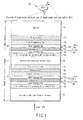
- FIG. 1 shows an example of the configuration of the layers of an optical recording medium (RW- or RAM-type phase-change recording optical disk) 100 according to an embodiment of the invention.
- the optical recording medium 100 which is a multilayer optical disk with a plurality of information layers (here, two layers, L0 and L1), includes an L0 information layer 19, an interlayer separating layer (or adhesive layer) 18, an L1 information layer 20 when viewed from the laser light incident side.
- the L0 information layer 19 is composed of a first interference film (also called protective film or dielectric film -- the same holds hereinafter) 11a, a lower interface film 12a, an L0 recording film 13a, an upper interface film 14a, a second interference film 15a, a reflecting film 16a, and a third interference film 17a stacked one on top of another in that order on a substrate 1a transparent to laser light to be used (or a short-wavelength laser beam whose wavelength is 405 nm or less).
- a first interference film also called protective film or dielectric film -- the same holds hereinafter
- the L1 information layer 20 is composed of a reflecting film 16b, a second interference film 15b, an upper interface film 14b, an L1 recording film 13b, a lower interface film 12b, and a first interference film 11b stacked one on top of another in that order in the opposite direction on a transparent substrate 1b.
- the optical recording medium (RW- or RAM-type phase-change recording optical disk) 100 of the embodiment has a structure that has a first interference film of the L1 information layer 20 and a third interference film 17 of the L0 information layer 19 bonded together with the interlayer separating layer 18 as an adhesive.
- the stacked structure (19) of the L0 information layer also assumes the role of a dielectric film (ZnS-SiO2 or the like: 17a) where the third interference layer contributes to optical enhancement and/or thermal diffusion.
- An ultrathin oxide film 21a is formed to a specific thickness (an average thickness of about 0.1 nm to 1.0 nm) on at least one (preferably both) of the upper and lower surfaces of the L0 recording film 13a.
- An ultrathin oxide film 21b is formed to a specific thickness (an average thickness of about 0.1 nm to 1.0 nm) on at least one (preferably both) of the upper and lower surfaces of the L1 recording film 13b.
- These ultrathin oxide films 21a, 21b are made up of the same constituent elements (Ge, Te, and the like) as those of the recording films 13a, 13b.
- the component parts shown by the same reference numerals except for suffixes a, b indicate component parts with similar functions.
- the L0 recording film 13a differs physically from the L1 recording film 13b in component parts, but they are similar to each other in the function of recording information.
- the first interference layers 11a and 11b are similar to each other in a dielectric film, they are not necessarily similar to each other in the function of a protective film (thus, expressed as "protective film or dielectric film"). That is, in a state where the L1 information layer 20 is formed on the substrate 1b (before being laminated with the adhesive layer 18), the first interference layer 11b can function as a protective layer (for the recording film).
- the first interference layer 11a need not function as a protective layer (because the substrate 1a covers the first interference layer 11a). In this case, before being bonded with the adhesive layer 18, it is more likely that the third interference layer 17a will function as a protective layer.
- film in interference film, interface film, and others may be called “layer” as needed, there is basically no difference between them.
- the reference numerals without suffixes a, b indicate equivalency to those with the suffixes a, b (for example, in the case of the interference layer 11, it indicates equivalency to 11a or 11b).
- the configuration of the phase-change recording medium of the embodiment is not limited to what is shown in FIG. 1.
- another dielectric film (not shown) may be provided between the second interference layer 15a (or 15b) and the reflecting film 16a (or 16b). All of the interference layers (11a, 11b, 15a, 15b, 17a, 17b) may be replaced with the material of the interface films (12a, 12b or 14a, 14b) and the interference layers may be eliminated.
- the reflecting film (16a or 16b) may be composed of a plurality of metal films stacked one on top of another. On the reflecting film (16a or 16b), an additional dielectric film (not shown) may be provided.
- the first information layer (L0 information layer) 19 side close to the light incident face configured as described above and the second information layer (L1 information layer) 20 side far away from the light incident face are formed. These are bonded together with the adhesive layer 18, thereby separating the layers.
- a multilayer medium with three layers or more (although not shown, when an information layer includes three layers, a second interlayer separating layer and an L2 information layer are further stacked between the substrates 1a and 1b of FIG. 1; and when an information layer includes four layers, a second and a third interlayer separating layer and an L2 and an L3 information layer are further stacked between the substrates 1a and 1b of FIG. 1).
- the medium may be such that various films are formed on the substrate 1a and/or 1b and, to the resulting film, a thin transparent sheet (not shown) of about 0.1 mm thick is laminated, and light is caused to enter via the transparent sheet (this type of medium is based on the assumption that an objective lens with a high NA of about 0.85 is used). The reason is that, even if a thin transparent cover layer of about 0.1 mm thick is used on the light incident side, this doesn't make much difference to the characteristics required for the recording film, interface layer material, protective film material, and reflecting film material used in the embodiment of FIG. 1 (when a 0.6-mm-thick transparent substrate is used).
- a preferred optical recording medium (or phase-change optical disk) has the following configuration and/or characteristics.
- the atomic binding form in the film was clarified by XPS, IR (infrared spectroscopy) measurement, or the like.
- the thermal conductivity and thermal diffusivity of the thin film and the interface thermal resistance between stacked thin films were evaluated using a thermoreflectance method.
- the DOS for the valance band of the recording film can be measured using XPS, UPS, or HX-PES (Hard X-ray Photo Electron Spectroscopy) techniques. Information on the state density can be obtained by measuring the electronic specific heat.
- FIG. 2 shows an example of the configuration of a sample used in measuring the DOS for the valance band of a recording film.
- Polycarbonate (PC) or the like is used for a substrate 1 of FIG. 2.
- the following films are formed using a sputtering apparatus.
- an interference film (ZnS-SiO2) 15, an interface layer 14, a recording film layer 13, an interface layer 12, an interference film (ZnS-SiO2) 11, and others are formed in that order.
- a reflecting film (Ag alloy) 16 provided far away from the laser light incident side, a reflecting film (Ag alloy) 16, an interference film (ZnS-SiO2) 15, an interface layer 14, a recording film layer 13, an interface layer 12b, an interference film (ZnS-SiO2) 11, and others are formed on the substrate in that order.
- the DOS for the valance band of the recording film is measured mostly by the HX-PES (Hard X-ray PhotoElectron Spectroscopy) method or XPS method.
- HX-PES Hard X-ray PhotoElectron Spectroscopy
- XPS X-ray PhotoElectron Spectroscopy
- FIG. 2 a sample shown in FIG. 2 is used which is composed of a substrate 1, a recording film 13 capable of changing the atomic arrangement reversibly, films 11 and 14 which are in contact with the recording film 13 and have a crystallization enhancing function, a protective film 11, and a reflecting film 16.
- the recording film 13 is amorphous in an as depo. state.
- the recording film is crystallized (or laser-annealed) using an initializing apparatus.
- the recording film can be crystallized by heating the film to a temperature higher than a crystallization temperature for a specific time with an electric furnace or the like.
- the energy of the top of the DOS for the valance band corresponds to Fermi energy in a conductor.
- the Fermi energy lies almost in the middle of the band gap between the valance band and the conduction band.
- a semiconductor may form a localized level, with the result that the Fermi potential goes up and down slightly.
- a method of controlling the ratio of the DOS of the crystalline state to the DOS of the amorphous state (the DOS of the crystalline state/the DOS of the amorphous state) at an energy level lower than the top of the DOS for the valence band of the recording film in the crystalline state and amorphous state includes (i) changing slightly the composition of the recording film in the direction of its thickness, (ii) selecting suitably interface layer materials provided over and under the recording film and changing elements doped in minute amounts from the interface layer to the recording film (micro reaction), and (iii) providing an ultrathin oxide film whose average thickness is 0.1 nm or more and 1 nm or less and which is made up of the elements constituting the recording film in a region in contact with the recording film.
- the crystallization speed over the recording film can be made different from that under the recording film by (i) changing slightly the composition of the recording film in the direction of its thickness and/or (ii) selecting suitably interface layer materials provided over and under the recording film and changing elements doped in minute amounts from the interface layer to the recording film.
- Te is less liable to be oxidized than Ge and Bi in the GeBiTe series. That is, Ge and Bi are more liable to be oxidized than Te.
- Te is less liable to be oxidized than Ge and Bi in the GeBiTe series. That is, Ge and Bi are more liable to be oxidized than Te.
- the recording film has more nuclears than a conventional recording film, which contributes to high-speed crystallization. Since which of the elements shows a micro reaction or is doped depends on a recording film and an interface layer to be used and their processes, control can be performed by selecting these suitably. By doing this, it is possible to make the crystallization speed over the recording film differ from that under the recording film, which is seemingly difficult to control.
- FIG. 3 is a diagram to help explain a manufacturing apparatus for optical recording mediums (or phase-change optical disks) according to an embodiment of the invention.
- a PC substrate supporting disk-like rotating base 102A is provided in such a manner that the rotating surface is horizontal in the figure (or perpendicular to the sheet of paper).
- a PC substrate is supported on the underside of the rotating base 102A in such a manner that the substrate is rotated by a motor 110A (or the substrate may not be rotated in another embodiment).
- an anode plate 104A on which a sputtering source (or target material) is provided so as to face the rotating base 102A.
- a magnet 111A configured to be rotatable is provided on the underpart of the anode plate 104A.
- the rotating base (or cathode plate) 102A is grounded.
- a RFpower supply unit 112A is connected in the case of RF sputtering (or a DCpower supply unit 112A is connected in the case of DC sputtering).
- the output voltage of the power supply unit 112A is applied between the grounded cathode plate 102A and the anode plate 104A.
- the vacuum container 100A is connected via a gas exhaust port 113A to an exhaust unit 114A.
- a trace of sputtering gas (inert gas, such as argon, and others) is injected from a gas cylinder 116 via a gas introduction port 115A and a control valve 118A into the vacuum container 100A sufficiently evacuated by the exhaust unit 114A.
- the amount of sputtering gas injected is checked by an inner-pressure sensor (or vacuum gauge) 108A provided on the vacuum container 100A.
- the substrate rotating motor 110R, magnet 111A, sputtering power supply unit 112A, exhaust unit 114A, and control valve 118 are computer-controlled by a sputtering control unit 120A.
- a monitor unit 106A having a film thickness measuring function.
- the CPU of the control unit 120A causes the monitor unit 106A to monitor the amount of sputtering from the sputtering source to the substrate. Specifically, while monitoring the thin film sputtered on the substrate, the CPU of the control unit 120A is programmed so as to adjust the RF power from the power supply unit 112A to the anode plate 104A so that the thin film layer may have a specific composition (or a specific film thickness).
- the vacuum container 100A of FIG. 3 has a load lock chamber and a process chamber, which are designed to function independently in sputtering.
- FIG. 4 is a flowchart to help explain the manufacturing processes of optical recording mediums (or phase-change optical disks) according to an embodiment of the invention.
- a substrate 1a/1b is placed on a specific part of the sputtering apparatus (manually or with a robot arm) (ST100) and the load lock chamber in the vacuum container 100A is vacuumized (ST102).
- the inner-pressure sensor 108A has sensed that the degree of vacuum in the load lock chamber is equal to or below, for example, 1 ⁇ 10 -3 (Pa) (Yes in ST104)
- the substrate is moved to the process chamber in the vacuum container 100A (ST106).
- the substrate on the cathode plate 102A side is rotated and at the same time, the magnet 111A on the anode plate 104A side is rotated (ST108).
- step ST106 to step ST116 are executed again.
- the target material is changed to the corresponding target material and, if necessary, the components of the gas introduced into the chamber are changed.
- argon may be used as the gas or a mixed gas of argon and nitrogen may be used.
- the rotation of the substrate on the cathode plate 102A side and the rotation of the magnet on the anode plate 104A side are stopped (ST120). Thereafter, the substrate on which the films have been formed is transported to the load lock chamber (ST122), outside nitrogen or air is leaked into the load lock chamber to release the vacuum state, and the substrate 1a/1b after the formation of the films is taken out (manually or with the robot arm) (ST124). Thereafter, the substrates 1a and 1b after the formation of the films are bonded together as shown in FIG. 1, thereby completing a single-sided multilayer optical disk (such as a high-density recording DVD-RN/RAM).
- a single-sided multilayer optical disk such as a high-density recording DVD-RN/RAM
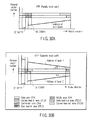
- FIGS. 5A, 5B, and 5C are diagrams showing a state where the elements (including Ge and Te) constituting the recording film of the optical recording medium (or phase-change optical disk) according to the embodiment have a segregation or a concentration distribution.
- the elements including Ge and Te
- there are various elements constituting the recording film see FIG. 8). To make it easy to understand a segregation or a concentration distribution of constituent elements, only Ge and Te are shown as a representative elements.
- FIG. 5A schematically shows a concentration [at.%] of an element in the range of a distance of several nanometers from the interface between the recording film (13a or 13b) and the lower interface film (12a or 12b) toward the lower interface film, in the range of a distance of several nanometers from the interface between the recording film (13a or 13b) and the upper interface film (14a or 14b) toward the upper interface film, and in the range of a distance of about 10 nanometers from the interface of the recording film (13a or 13b) in these ranges.
- a part (e.g., Ge) of the constituent elements of the recording film segregates in a pattern toward the high concentration side in the range of the recording film and the other part (e.g., Te) of the constituent elements of the recording film segregates in another pattern toward the high concentration side in the range of the recording film.
- FIGS. 5B and 5C schematically show different examples of a segregation pattern.
- the difference in element concentration between Ge and Te is smaller than in FIG. 5A.
- the positions (in the horizontal direction in the figure) where the element concentration of Ge and that of Te change appear on the side opposite to that in FIG. 5A.
- the concentration of the constituent element may be lower near the middle position in the direction of the thickness of the recording film than its shoulder portion.
- FIG. 6 is a table showing an example of the materials of an interface layer (upper interface film and/or lower interface film) of the optical recording medium (or phase-change optical disk) according to the embodiment.
- FIG. 7 is a table exemplifying the composition ratio of Ge and N when GeN is used as a material for the interface layer.
- FIG. 8 is a table showing an example of the materials of a recording film (L0 and/or L1) of the optical recording medium (or phase-change optical disk) according to the embodiment.
- FIG. 9 is a table to help explain comparative examples 1 to 3 when there is no interface layer and when SiO2 and Y2O3 are used for an interface layer.
- FIGS. 6 and 8 were applied to a sample with the configuration of FIG. 2 and experiments were conducted. Any one of the interface layer materials shown in FIG. 6 was provided on the light incident side (or on the 12 side) and any one of the remaining interface materials was selected and arranged on the reflecting film side (or on the 16 side). As for the compounds whose composition can be changed, such as GeN or GeCrN, some of the combinations differing in composition are suitable for the interface layer material. FIG. 7 shows a case where the composition of GeN was changed. As for a comparative example, experiments were done on interface layer materials shown in FIG. 9.
- FIG. 10 is a table exemplifying the result of measuring the ratio of the DOS of the crystalline state to the DOS of the amorphous state (the DOS of the crystalline state/the DOS of the amorphous state: for example, au11/au12 in FIG. 20) at an energy level 0.5 [eV] lower than the top of the DOS for the valence band of the recording film, for combinations of various interface layer materials.
- FIG. 11 is a table exemplifying the result of measuring the ratio of the DOS of the crystalline state to the DOS of the amorphous state (the DOS of the crystalline state/the DOS of the amorphous state: for example, au01/au02 in FIG. 19) for combinations of interface layer materials (including a case where no interface layer is used) different from those of FIG. 10.
- FIGS. 10 and 11 shows the result of measuring the ratio of the DOS of the crystalline state to the DOS of the amorphous state (the DOS of the crystalline state/the DOS of the amorphous state) at an energy level 0.5 [eV] lower than the top of the DOS for the valence band of the recording film, for combinations of various interface layer materials.
- the ratio of the DOS of the crystalline state to the DOS of the amorphous state (the DOS of the crystalline state/the DOS of the amorphous state) at an energy level 0.5 [eV] lower than the top of the DOS for the valence band of the recording film was 1.0 or more and 2.5 or less.
- the ratio for any combination was 4 or more.
- FIG. 19 is a diagram to help explain the ratio of the DOS of the crystalline state to the DOS of the amorphous state (the DOS of the crystalline state/the DOS of the amorphous state) at an energy level 0.5 [eV] lower than the top of the DOS for the valance band of the recording film, when there is no interface layer.
- FIG. 20 is a diagram to help explain the ratio of the DOS of the crystalline state to the DOS of the amorphous state (the DOS of the crystalline state/the DOS of the amorphous state) at an energy level 0.5 [eV] lower than the top of the DOS for the valance band of the recording film, when there is an interface layer.
- An optical recording medium that has a favorable characteristic (see FIG. 10 and FIGS. 13 to 16) is recorded into and erased from reversibly with light. It comprises a substrate, a recording film capable of changing an atomic arrangement reversibly, a film which is in contact with the recording film and has a crystallization enhancing function, a protective film, a reflecting film, and a dielectric film contributing to optical enhancement and/or thermal diffusion, with the ratio of the DOS of the crystalline state to the DOS of the amorphous state (the DOS of the crystalline state/the DOS of the amorphous state) at an energy level 0.5 [eV] lower than the top of the DOS for the valance band of the recording film being 1.0 or more and 2.5 or less.
- the energy of the top of the DOS for the valance band is Fermi energy (Fermilevel).
- the Fermi energy has a fluctuation of about 25 [meV] at room temperature.
- the inventors of this application used an energy level 0.5 [eV] lower than the top of the DOS for the valance band as a reference.
- a similar tendency appears from the top of the DOS for the valance band to an energy level about 1.0 [eV] lower than the top (further from the top of the DOS for the valance band to an energy level about 0.25 [eV] lower than the top).
- the inventors after having hunted for the condition for a high S/N ratio, the inventors have selected the aforementioned reference (or an energy level 0.5 [eV] lower than the top of the DOS for the valance band) as the most favorable one.
- the ratio of the DOS of the crystalline state to the DOS of the amorphous state (the DOS of the crystalline state/the DOS of the amorphous state) at an energy level 0.5 [eV] lower than the top of the DOS for the valance band of the recording film becomes 2.5 or less, this suggests that the crystalline state and amorphous state are close to each other in terms of electronic state, and that the amorphous state has a higher short-range regularity.
- the phase transition from the crystalline state to the amorphous state or vice versa becomes easy, which enables a high-speed phase transition from crystalline to amorphous or vice versa.
- the crystalline state is identical with the amorphous state in terms of electronic state, and therefore the amorphous state has a much higher short-range regularity. As a result, a higher-speed phase transition from crystalline to amorphous or vice versa becomes possible.
- the ratio of the DOS of the crystalline state to the DOS of the amorphous state (the DOS of the crystalline state/the DOS of the amorphous state) at an energy level 0.5 [eV] lower than the top of the DOS for the valance band of the recording film is 2.5 or more, this suggests that the crystalline state and amorphous state differ from each other in terms of both of crystalline state and electronic state and the short-range regularity in the amorphous state decreased greatly. Since there is almost no long-range regularity in the amorphous state, the phase transition from the crystalline state to the amorphous state or vice versa requires considerable energy, which makes it impossible to perform phase transition at high speed.
- an optical recording medium is suitable where the ratio of the DOS of the crystalline state to the DOS of the amorphous state (the DOS of the crystalline state/the DOS of the amorphous state) at an energy level 0.5 [eV] lower than the top of the DOS for the valance band of the recording film is 1.0 or more and 2.5 or less.
- a film with a crystallization enhancing function or the interface films 12a, 12b/14a, 14b
- the interface film which is in contact with the recording film and has a crystallization enhancing function is configured to include germanium nitride (GeN), germanium-chrome nitride (GeCrN), zirconium oxide (ZrO2), stabilized zirconia + chrome oxide (ZrO2+Cr2O3), stabilized zirconia + silicon oxide + chrome oxide (ZrO2+SiO2+Cr2O3), zircon + chrome oxide (ZrSiO4 + Cr2O3), or hafnium oxide (HfO2).
- the interface film may be composed of a compound (HfO 2-x N x ) containing hafnium (Hf), oxygen (0), and nitrogen (N).
- the interface film may be composed of a film ((ZrO 2-x N x ) 1-y ((Y 2 O 3 ) 1-z (Nb 2 O 5 ) z ) y where 0 ⁇ z ⁇ 1) containing zirconium (Zr), oxygen (0), nitrogen (N), yttria (Y), and niobium (Nb).
- the interface film may be configured to include chrome oxide (Cr2O3), zinc oxide (ZnO), zinc oxide + tantalum oxide (ZnO+Ta2O5), zinc oxide + tantalum oxide + indium oxide (ZnO+Ta2O5+In2O3), tin oxide (SnO2), tin oxide + antimony oxide (SnO2+Sb2O3), tin oxide + tantalum oxide (SnO2+Ta2O5), or tin oxide + niobium oxide (SnO2+Nb2O5).
- Cr2O3 chrome oxide
- ZnO zinc oxide
- ZnO+Ta2O5 zinc oxide + tantalum oxide + indium oxide
- ZnO+Ta2O5+In2O3 zinc oxide + tantalum oxide + indium oxide
- the effect of the invention is more noticeable.
- the Ge-to-Sn replacement ratio should be Sn/Ge ⁇ 0.5 and the Sn-to-Bi replacement ratio should be Bi/(Bi+Sb) ⁇ 0.7.
- the ratio of In to Sb or Bi in amount should be 0.7 or less, preferably 0.5 or less, and more preferably 0.25 or less.
- the crystallization enhancing function is closely related to the crystallization temperature, melting point, and the like. Therefore, although the optimum condition differs depending on the design of a medium, it is preferable to select the amount in the above range.
- a recording film is composed of GeBiTe and a so-called pseudo-binary-series linear composition and its vicinity are used which enable a representation of (GeTe)-(Bi2Te3)
- the effect of the interface film of the invention is noticeable.
- an alloy recording film material with the (GeTe)-(Bi2Te3) composition and its vicinity, the Ge composition ratio being 30 at.% or more is used as the interface film of the invention, the effect of the invention is particularly noticeable.
- the recording film includes nitrogen (N), it can be represented as a composition where nitrogen (N) is added to (GeTe)-(Sb2Te3), or (GeTe)-(Sb2Te3)-N. That is, the composition is such that nitrogen (N) is added to a pseudo-binary series of (GeTe)-(Sb2Te3). It can be represented more simply as GeSbTe-N.
- a recording film nitrided this way is used, the effect of the interface film of the invention is remarkable.
- an alloy recording film material with the (GeTe)-(Sb2Te3) composition and its vicinity, the Ge composition ratio being 30 at.% or more, is used as the interface film of the invention, the effect of the invention is particularly noticeable.
- the effect of the invention is more noticeable.
- the Ge-to-Sn replacement ratio should be Sn/Ge ⁇ 0.5 and the Sn-to-Bi replacement ratio should be Bi/(Bi+Sb) ⁇ 0.7.
- the ratio of In to the amount of Bi should be 0.7 or less, preferably 0.5 or less, and more preferably 0.25 or less.
- the amount of these replacement elements and the amount of nitrogen but also the crystallization enhancing function is closely related to the crystallization temperature, melting point, and the like. Therefore, although the optimum condition differs depending on the design of a medium, it is preferable to select the amount in the above range.
- the recording film is configured to have a composition where nitrogen (N) is added to (GeTe)-(Bi2Te3), or a so-called pseudo-binary-series linear composition and its vicinity represented as (GeTe)-(Bi2Te3)-N (more simply represented as GeBiTe-N), the effect of the interface film of the invention is remarkable.
- the effect of the invention is particularly remarkable.
- the effect of the invention is produced, regardless of the thickness of the recording film.
- the thickness of the recording film is made 20 nm or less, more preferably 10 nm, the effect is more noticeable.
- a recording medium of the type that allows light to enter one side of the medium and enables two different information layers to be accessed the single-sided, dual-layer type
- the effect of the invention is noticeable.
- the advantage in that case is that the film thickness of the recording layer can be made 10 nm or less.
- Use of an interface layer related to the embodiment makes the following advantages noticeable: the transmittance to short-wavelength laser light can be made higher and the contrast can be increased.
- the inventors of this application conducted experiments using germanium nitride (GeN), silicon carbide (Si-C), silicon nitride (Si-N), Ta2O5+SiC, and the like which are well known as interface film materials having an effect on the enhancement of crystallization of the recording film.
- germanium nitride GeN
- Si-C silicon carbide
- Si-N silicon nitride
- Ta2O5+SiC silicon nitride
- the following tradeoff was found: using a material with a high crystallization enhancing effect without controlling the state of the recording film resulted in a decrease in CNR and a material with high CNR had a poor crystallization enhancing effect.
- a substrate compatible with both of the land-groove recording method (a) and groove recording method (b) was used as the substrate of FIG. 1.
- a 0.59-mm-thick polycarbonate (PC) substrate formed by injection molding was used in the land-groove recording method (a). Since grooves were formed with a groove pitch of 0.68 ⁇ m, when data was recorded to both lands (L) and grooves (G), the pitch corresponded to a track pitch of 0.34 ⁇ m.
- the groove recording method (b) a 0.59-mm-thick PC substrate formed by injection molding was also used. The groove pitch was set at 0.4 ⁇ m.
- an interference film (ZnS-SiO2) 15a, an interface layer 14a, a recording film layer 13a, an interface layer 12a, and an interference film (ZnS-SiO2) 11a are formed in that order.
- a reflecting film (Ag alloy) 16b, an interference film (ZnS-SiO2) 15b, an interface layer 14b, a recording film layer 13b, an interface layer 12b, and an interference film (ZnS-SiO2) 11b are formed on the PC substrate in that order.
- the sputtering apparatus used is a so-called Cluster sputter film-forming apparatus which forms each layer by sputtering in a different film-forming chamber.
- the Cluster sputter film-forming apparatus comprises a load-lock chamber in which a substrate is installed, a transport chamber, and a process chamber which forms each film.
- FIG. 3 shows an example of the configuration of one process chamber.
- the process chamber is composed of a unit which evacuates the chamber, a vacuum gauge, a pressure sensor, a film thickness meter, a sputtering target serving as a material on which a film is to be formed, and a substrate installed.
- Such rare gas as Ar is mainly used as sputter gas. Oxygen or nitrogen gas may be used as needed.
- FIG. 4 is a flowchart to help explain the process of forming a film.
- FIG. 21 is a GeSbTe ternary phase diagram to help explain a favorable composition range of the recording film of an optical recording medium according to an embodiment of the invention.
- FIG. 22 is a GeBiTe ternary phase diagram to help explain a favorable composition range of the recording film of an optical recording medium according to an embodiment of the invention.
- FIG. 23 is a Ge/Sn-Sb/Bi-Te ternary phase diagram to help explain a favorable composition range of the recording film of an optical recording medium according to an embodiment of the invention (when Ge and/or Sb is replaced with Sn and/or Bi in FIG. 21).
- This embodiment shows a case where a GeSbTeBi-series recording film was used.
- the film thickness of the recording film was set to 10 nm or less.
- ZrO2 was used on the light incident side and Cr2O3 was used on the reflecting film side.
- the ZnS-SiO2 film (or interference film) was formed using a target obtained by mixing SiO2 with ZnS.
- the sputtering apparatus used is a so-called Cluster sputter film-forming apparatus which forms each layer by sputtering in a different film-forming chamber. After each medium is formed, the reflectivity and transmittance of the medium are measured with a spectrophotometer.
- FIG. 12 is a table exemplifying the condition for evaluation when a recording film is evaluated by a land-groove recording method.
- the optimum power in measuring the SbER was set as the sensitivity of the medium.
- L0 with the configuration of the embodiment was bonded to a blank disk on which no film had been formed and L1 was bonded to a blank disk on which no film had been formed.
- each evaluation was made at a linear velocity of 5.4 m/s (constant velocity) in the land-groove recording method (a) and at a linear velocity of 6.61 m/s (constant velocity) in the groove recording method (b).
- FIG. 13 is a table showing an example of the result (CNR, SbER, ER) of evaluating a recording film for a plurality of samples.
- FIG. 13 shows the results of evaluations excluding the result of the number of OWs.
- SbER was 1.8 ⁇ 10 -6 or less in both lands and grooves and the number of OWs was 2000 or more, assuring practical characteristics.
- the evaluation of the OW characteristic was made 10000 times or more, it was found that about 10000 OWs were possible.
- the comparison of analog data was made.
- CNR was 52.9 dB or more in both lands and grooves
- the erase ratio was -33.8 dB or less
- cross erase was -0.1 dB or less, which were excellent results.
- a disk was made by forming a film configuration of the embodiment on a 1.1-mm-thick polycarbonate (PC) substrate formed by injection molding and providing a 75- ⁇ m-thick transparent cover layer on the film.
- a substrate with a groove pitch of 0.32 ⁇ m was evaluated in groove recording, that is, by the groove recording method (b).
- CNR was 52 dB or more
- the erase ratio was -30 dB or less
- OW characteristic showed 2000 times or more, which were very good results. Accordingly, it is conceivable that the interface layer material of the embodiment is favorable because it is not affected by the thickness of the substrate or the thickness of the cover layer on the light incident side.
- FIG. 14 is a table showing another example of the result (ER when the linear velocity is changed) of evaluating the recording film for a plurality of samples.
- the erase ratio was measured, while the linear velocity was being changed.
- FIG. 14 shows the result. All measured values show a good erasing characteristic.
- the result of analyzing a disk produced in the same manner as the evaluated medium has shown that the recording film had a segregation or concentration distribution as shown in FIGS. 5A, 5B, and 5C.
- the recording film had a segregation or concentration distribution as shown in FIGS. 5A, 5B, and 5C.
- Ge, Sb, and Bi were rich and Te was poor in the vicinity of one interface (on the left side in FIG. 5) (only the elements Ge and Te are shown in FIGS. 5A, 5B, and 5C for clarity).
- a disk was made by using GeCrN on the light incident side of the interface layer and Cr2O3 on its reflecting film side.
- the same experiment as that in embodiment 2 was conducted.
- SbER was on the order of 10 -6 in both lands and grooves for any sample as shown in FIG. 13, achieving a good error rate.
- CNR was 52 dB or more in both lands and grooves for any sample, producing an excellent result.
- the number of OWs was 2000 times or more in any medium, assuring practical characteristics.
- a disk was made by using ZrO2+Y2O3+CrO3 on the light incident side of the interface layer and SnO2+Sb2O3 on its reflecting film side.
- SbER was on the order of 10 -6 in both lands and grooves for any sample as shown in FIG. 13, achieving a good error rate.
- CNR was 52 dB or more in both lands and grooves for any sample, producing an excellent result.
- the number of OWs was 2000 times or more in any medium, assuring practical characteristics.
- a disk was made by using ZrSiO4+Cr2O3 on the light incident side of the interface layer and Cr2O3 on its reflecting film side.
- SbER was on the order of 10 -6 in both lands and grooves for any sample as shown in FIG. 13, achieving a good error rate.
- CNR was 53 dB or more in both lands and grooves for any sample, producing an excellent result.
- the number of OWs was 2000 times or more in any medium, assuring practical characteristics.
- a disk was made by using ZrO2+Y2O3+SiO2+Cr2O3 on the light incident side of the interface layer and ZnO+Ta2O5+In2O3 on its reflecting film side.
- SbER was on the order of 10 -6 in both lands and grooves for any sample as shown in FIG. 13, achieving a good error rate.
- CNR was 53 dB or more in both lands and grooves for any sample, producing an excellent result.
- the number of OWs was 2000 times or more in any medium, assuring practical characteristics.
- SbER was on the order of 10 -6 in both lands and grooves for any sample as shown in FIG. 13, achieving a good error rate.
- CNR was 53 dB or more in both lands and grooves for any sample, producing an excellent result.
- the number of OWs was 2000 times or more in any medium, assuring practical characteristics.
- SbER was on the order of 10 -6 in both lands and grooves for any sample as shown in FIG. 13, achieving a good error rate.
- CNR was 52 dB or more in both lands and grooves for any sample, producing an excellent result.
- the number of OWs was 2000 times or more in any medium, assuring practical characteristics.
- a disk was made by using GeN on the light incident side of the interface layer and Cr2O3 on its reflecting film side.
- the same experiment as that in embodiment 2 was conducted.
- SbER was on the order of 10 -6 in both lands and grooves for any sample as shown in FIG. 13, achieving a good error rate.
- CNR was 53 dB or more in both lands and grooves for any sample, producing an excellent result.
- the number of OWs was 2000 times or more in any medium, assuring practical characteristics.
- SbER was on the order of 10 -6 in both lands and grooves for any sample as shown in FIG. 13, achieving a good error rate.
- CNR was 53 dB or more in both lands and grooves for any sample, producing an excellent result.
- the number of OWs was 2000 times or more in any medium, assuring practical characteristics.
- a disk was made by using Cr2O3 on the light incident side of the interface layer and ZnO+Ta2O5 on its reflecting film side.
- the same experiment as that in embodiment 2 was conducted.
- SbER was on the order of 10 -6 in both lands and grooves for any sample as shown in FIG. 13, achieving a good error rate.
- CNR was 51 dB or more in both lands and grooves for any sample, producing an excellent result.
- the number of OWs was 2000 times or more in any medium, assuring practical characteristics.
- a disk was made by using GeN on the light incident side of the interface layer and SnO2+Ta2O5 on its reflecting film side.
- the same experiment as that in embodiment 2 was conducted.
- SbER was on the order of 10 -6 in both lands and grooves for any sample as shown in FIG. 13, achieving a good error rate.
- CNR was 53 dB or more in both lands and grooves for any sample, producing an excellent result.
- the number of OWs was 2000 times or more in any medium, assuring practical characteristics.
- a disk was made by using ZrO2+Y2O3+Cr2O3 on the light incident side of the interface layer and ZnO+Ta2O5+In2O3 on its reflecting film side.
- SbER was on the order of 10 -6 in both lands and grooves for any sample as shown in FIG. 13, achieving a good error rate.
- CNR was 53 dB or more in both lands and grooves for any sample, producing an excellent result.
- the number of OWs was 2000 times or more in any medium, assuring practical characteristics.
- the land-groove recording method (a) a 0.6-mm-thick polycarbonate (PC) substrate formed by injection molding was used. Since grooves were formed with a groove pitch of 0.68 ⁇ m, when data was recorded to both lands (L) and grooves (G), the pitch corresponded to a track pitch of 0.34 ⁇ m.
- the groove recording method (b) a 0.59-mm-thick PC substrate formed by injection molding was used. The groove pitch was set at 0.4 ⁇ m.
- the following films were formed using a sputtering apparatus: ZnS-SiO2, SiO2, ZnS-SiO2, an interface layer, a recording film layer, an interface layer, ZnS-SiO2, and Ag alloy in that order, starting from the light incident side. Then, the resulting disk was bonded to a blank disk with no film by UV cured resin.
- the sputtering apparatus used in the same manner as in embodiment 2 is a so-called Cluster sputter film-forming apparatus which forms each layer by sputtering in a different film-forming chamber.
- compositions were examined.
- a case where a GeSbTeBi-series recording film was used is shown.
- the thickness of the recording film was set to around 10 nm or less.
- GeN was used on the light incident side and Cr2O3 was used on the reflecting film side.
- a ZnS-SiO2 film was formed using a target obtained by mixing SiO2 with ZnS.
- the sputtering apparatus used is a so-called Cluster sputter film-forming apparatus which forms each layer by sputtering in a different film-forming chamber. After each medium was formed, the reflectivity and transmittance of the medium were measured with a spectrophotometer.
- the land-groove recording method (a) a 0.6-mm-thick polycarbonate (PC) substrate formed by injection molding was used. Since grooves were formed with a groove pitch of 0.68 ⁇ m, when data was recorded to both lands (L) and grooves (G), the pitch corresponded to a track pitch of 0.34 ⁇ m.
- the groove recording method (b) a 0.59-mm-thick PC substrate formed by injection molding was used. The groove pitch was set at 0.4 ⁇ m.
- the following films were formed using a sputtering apparatus: ZnS-SiO2, SiOC, ZnS-SiO2, an interface layer, a recording film layer, an interface layer, ZnS-SiO2, and Ag alloy in that order, starting from the light incident side. Then, the resulting disk was bonded to a blank disk with no film by UV cured resin.
- the SiOC film was formed by subjecting a SiC-system target to reactive sputtering using a mixed gas of Ar/02. The SiOC film has almost the same low refractive index as that of SiO2. The same experiment as that in embodiment 2 was conducted.
- SbER was on the order of 10 -6 in both lands and grooves for any sample as shown in FIG. 13, achieving a good error rate.
- CNR was 51 dB or more in both lands and grooves for any sample, producing an excellent result.
- the number of OWs was 2000 times or more in any medium, assuring practical characteristics.
- a disk was made by using GeN on the light incident side of the interface layer and Cr2O3 on its reflecting film side, or by using GeN on both the sides.
- This embodiment shows examples of disks using a GeSbTe-series, a GeSbTeSn-series, and a GeGiTe-series recording film layer whose representative examples are shown in FIG. 8. The same experiment as that in embodiment 2 was conducted on each disk. The results of the experiments are shown in FIG. 15.
- FIG. 15 is a table showing an example of the result (CNR, SbER) of evaluating recording films with various compositions.
- a disk was made by using GeCrN on the light incident side of the interface layer and Cr2O3 on its reflecting film side.
- FIG. 16 is a table showing an example of the result (CNR, SbER) of evaluation when a small amount of N is added to recording films with various compositions. As shown in FIG. 16, both CNR and each SbER presented good characteristics. The number of OWs was 2000 times or more, assuring practical characteristics. After an environmental test, no peeling was found in the film. Nitrogen (N) was suitable in the range of 1 to 5 at.%, preferably in the vicinity of 3 at.%.
- FIGS. 17 and 18 list the characteristics of the disks.
- the same experiment as in embodiment 2 was conducted on each disk. The results are shown in FIGS. 17 and 18.
- FIG. 17 is a table showing an example of the result (CNR, SbER, ER) of evaluating comparative examples 1 to 3 when no interface layer was used and when SiO2 and Y203 were used for an interface layer.
- FIG. 18 is a table showing another example of the result (ER when the linear velocity was changed) of evaluating comparative examples 2 and 3 when SiO2 and Y203 were used for an interface layer.
- any one of CNR, SbER, and erase ratio presented an insufficient characteristic. Accordingly, the OW characteristic was not evaluated.
- One of the essential structural requirements in one embodiment of the invention is to set to 1.0 or more and 2.5 or less the ratio of the DOS of the crystalline state to the DOS of the amorphous state (the DOS of the crystalline state/the DOS of the amorphous state) at an energy level 0.5 [eV] lower than the top of the DOS for the valance band of the recording film in a phase-change optical recording medium which records data using a recording film that changes an atomic arrangement reversibly.
- the other films and others are not limited to the materials explained in the embodiment.
- minute amounts of, for example, Co, V, or Ag may be added to GeSbTe in the range that does not ruin the effect of the embodiment.
- minute amounts of, for example, Co, V, or Ag may be added to GeBiTe.
- the embodiment limits neither the thickness of the substrate nor the order in which films are formed.
- the embodiment may be applied to not only a medium which allows light to enter via a substrate on which films are to be formed but also a medium which allows light to enter via a transparent sheet laminated to a film-formed substrate.
- a recording medium whose transparent sheet on the light incident side is designed to be as thin as about 0.1 mm by using an objective lens with a high NA of about 0.85.
- the wavelength of the laser beam used is not limited to the vicinity of 405 nm.
- the interface layer is practically transparent up to a short wavelength range of about 350 nm to 250 nm and therefore the effect of the embodiment is useful.
- the phase-change optical recording medium comprises a substrate, a recording film capable of changing an atomic arrangement reversibly, a film which is in contact with the recording film and has a crystallization enhancing function, a protective film or a dielectric film, and a reflecting film.
- the optical recording film causes the elements constituting the recording film to have a segregation or a concentration distribution in the direction of the thickness of the recording film from a region in contact with the recording film, or in the in-plane direction of the recording film.
- phase-change recording medium which secures a high CNR and a low bit error rate, assures an excellent erasing ratio, achieves a good cross erase characteristic, and therefore is capable of recording and rewriting at higher speed in higher density than a conventional equivalent.
- FIG. 24 is a diagram to help explain the configuration of an information recording and reproducing apparatus according to an embodiment of the invention.
- a phase-change optical disk 100 according to the embodiment explained with reference to FIG. 1 and the like can be recorded into or reproduced from with the apparatus having the configuration as shown in FIG. 24.
- the part above a control section 143 represents mainly an information recording control system for an information storage medium.
- An embodiment of the information reproducing apparatus corresponds to the part excluding the information recording control system of FIG. 1.
- a thick solid-line arrow represents the flow of main information, i.e., a reproduced signal or a recording signal, a thin sold-line arrow the flow of information, a single-dot-dash line arrow a reference clock line, a thin broken line arrow the direction of the command destination.
- an optical head (not shown) is provided in an information recording and reproducing section 141.
- information is reproduced using PRML (Partial Response Maximum Likelihood) techniques, thereby achieving a higher recording density of an information storage medium.
- PRML Partial Response Maximum Likelihood
- PR (1, 2, 2, 2, 1) is used in this embodiment.
- the modulated channel bit train is recorded onto an information storage medium according to the (d, k; m, n) modulation rule (meaning RLL (d, k) in the m/n modulation in the above-described writing method).
- RLL Error to Twelve Modulation
- ETM Eight to Twelve Modulation
- the channel bit interval is shortened close to its limit, aiming at making the recording density of the information storage medium higher.
- PRML Partial Response Maximum Likelihood
- the signal reproduced at the information recording and reproducing section 141 is subjected to reproduced waveform correction at a PR equalizing circuit 130.
- an AD converter 169 samples the signal passed through the PR equalizing circuit 130 and converts the signal into a digital amount.
- the digital amount is then subjected to a Viterbi decoding process at a Viterbi decoder 156.
- the data after the Viterbi decoding process is treated as data identical with that binarized at a conventional slice level.
- PRML techniques are used, a shift in the sampling timing at the AD converter 169 increases the error rate of data after Viterbi decoding.
- the information reproducing apparatus or the information recording and reproducing apparatus particularly has a separate sampling timing extracting circuit (a combination of a Schmitt trigger binarizing circuit 155 and a PLL circuit 174).
- the Schmitt trigger binarizing circuit 155 has a specific range of slice reference level for binarization (actually the voltage value in the forward direction of the diode). Only when the specific range is exceeded does the binarizing circuit 155 binarize the signal. Therefore, for example, if the pattern "1010101010101010101010” has been input as described above, the signal amplitude is so small that binarization is not performed. If a rougher pattern, for example, "1001001001001001001001001" has been input, since the amplitude of the reproduced raw signal becomes larger, the switching between the polarities of a binarized signal is performed with the "1" timing at the Schmitt trigger binarizing circuit 155. In this embodiment, NRZI (Non-Return to Zero Invert) techniques are used and the position of "1" in the pattern coincides with the recording mark or the edge part (boundary part) of the pit.
- NRZI Non-Return to Zero Invert
- the PLL circuit 174 detects the difference in frequency and phase between the binarized signal output from the Schmitt trigger binarizing circuit 155 and the reference clock 198 signal sent from the reference clock generator 160 and changes the frequency and phase of the output clock of the PLL circuit 174.
- the reference clock generator 160 uses the output signal of the PLL circuit 174 and decoding characteristic information on the Viterbi decoder 156 (although not shown concretely, information on the convergence length (the distance to convergence) in the path metric memory in the Viterbi decoder 156), the reference clock generator 160 applies feedback to (the frequency and phase of) the reference clock 198 so that the error rate after Viterbi decoding may be decreased.
- the reference clock 198 generated at the reference clock generator 160 is used as reference timing in processing a reproduced signal.
- a synchronizing code position extracting section 145 detects the positions of synchronizing codes (sync codes) mixed in the output data string of the Viterbi decoder 156 and extracts the starting position of the output data. With the starting position as a reference, a demodulation circuit 152 demodulates the data temporarily stored in a shift register circuit 170. In the embodiment, the original bit train is restored by referring to a conversion table recorded in a demodulation conversion table recording section 154 for every 12 channel bits. Thereafter, an ECC decoding circuit 162 carries out an error correction process. Then, a descramble circuit 159 performs descrambling.
- address information has been recorded beforehand by wobble modulation.
- a wobble signal detecting section 135 reproduces the address information (that is, determines the contents of the wobble signal) and supplies information necessary to access a desired location to the control section 143.
- a data ID generating section 165 creates data ID information according to the recording location on the information storage medium.
- a CPR_MAI data generating section 167 creates copy control information
- a data ID, IED, CPR_MAI, EDC adding section 168 adds various pieces of information, including data ID, IED, CPR_MAI, and EDC to the information to be recorded.
- a descramble circuit 157 performs descrambling.
- an ECC encoding circuit 161 constructs an ECC block and a modulation circuit 151 converts the ECC block into a channel bit train
- a synchronizing code creating and adding section 146 adds a synchronizing code to the bit train
- the information recording and reproducing section 141 records the data onto the information storage medium.
- a DSV (Digital Sum Value) value computing section 148 calculates DSV values after modulation one after another. The values are fed back to code conversion in modulation.
- FIG. 25 is a diagram to help explain an example of the signal processing circuit using the PRML detecting method.
- FIG. 25 shows the signal processing circuit using the PRML method to reproduce a signal in the data are, data lead-in area, and data lead-out area.
- a quadrant photodetector 302 of FIG. 25 is fixed to the optical head existing in the information recording and reproducing section 141 of FIG. 24.
- a signal obtained by summing the sense signals from the respective light-detecting cells of the quadrant photodetector 302 is called a lead channel 1 signal.
- a detailed configuration of the PR equalizing circuit 130 of FIG. 24 is composed of the respective circuits ranging from a preamplifier circuit 304 to a tap controller 332, an equalizer 330, and an offset canceller 336 in FIG. 25.
- a PLL circuit 334 of FIG. 25 is a part of the PR equalizing circuit 130 of FIG. 24 and differs from the Schmitt trigger binarizing circuit 155 of FIG. 24.
- a primary cut-off frequency of the high-pass filter circuit 306 in FIG. 25 is set at 1 KHz.
- a 7-tap equalizer is used as the pre-equalizer circuit (because use of a 7-tap equalizer minimizes the circuit size and enables the reproduced signal to be detected with high accuracy).
- the sampling clock frequency of an A/D converter 324 is at 72 MHz and the digital output is an 8-bit one.
- the offset canceller 336 corrects the offset using the signal obtained from the output of the equalizer 330.
- an adaptive equalizing process is carried out at the PR equalizing circuit 130 of FIG. 24.
- a tap controller 332 is used which automatically modifies each tap coefficient in the equalizer using the output signal of the Viterbi decoder 156.
- FIG. 26 is a diagram to help explain the configuration of the Viterbi decoder according to the embodiment.
- FIG. 26 shows the configuration of the Viterbi decoder 156 of FIG. 24 or 25.
- a branch metric computing section 340 calculates the branch metric for all of the branches expected from the input signal and sends the calculated value to an ACS 342.
- the ACS 342 which stands for Add Compare Select, calculates the path metric by adding the branch metric for each of the expected paths and transfers the result of the calculation to a path metric memory 350.
- the ACS 342 does calculations also referring to the information in the path metric memory 350.
- a path memory 346 temporarily stores an expected situation of each path (transition) and the value of the path metric calculated at the ACS 342 according to the path.
- An output switching section 348 compares the path metric for each path with another and selects the path whose path metric value is the smallest.
- FIG. 27 is a diagram to help explain an example of state transition in PR (1, 2, 2, 2, 1) class. Since in the transitions of states expected in PR (1, 2, 2, 2, 1) class, only the one shown in FIG. 27 is possible, the Viterbi decoder 156 determines a path which can be present (or expected) in decoding, on the basis of the transition diagram of FIG. 27.
- FIG. 28 is a diagram to help explain an example of the structure and dimensions of an optical recording medium (or phase-change optical disk) according to an embodiment of the invention.
- FIG. 28 shows the structure and dimensions of an information storage medium of the embodiment. In the embodiment, the following three types of information storage medium are described:
- the three types of information storage medium share most of the structure and dimensions.
- a burst cutting area BCA a system lead-in area SYLDI, a connection area CNA, a data lead-in area DTLDI, and a data area DTA are arranged from the inner edge in that order.
- a data lead-out area DTLDO is provided on the outer edge part.
- a middle area MDA is provided on the outer edge part.
- SYLDI information is recorded in an emboss (prepit) form. This area is for reproduction only (prevents additional recording) in each of the recordable information storage medium and the rewritable one.
- a reproduce-only information storage medium information is recorded in an emboss (prepit) form in the data lead-in area DTLDI, whereas in a recordable and a rewritable information storage medium, the data lead-in area DTLDI enables new information to be recorded additionally (or rewriting in the rewritable type) by creating recording marks.
- areas enabling new information to be recorded additionally (or rewriting in the rewritable type) and reproduce-only areas where information is recorded in emboss (prepit) form are mixed in the data lead-out area DTLDO.
- the signals recorded there are reproduced by the PRML method, thereby achieving a higher recording density of the information storage medium (particularly an improvement in the linear density).
- the signals recorded there are reproduced by the slice level detecting method, thereby securing the interchangeability with an existing DVD and the stabilization of reproduction.
- the burst cutting area BCA and the system lead-in area SYLDI do not overlap with each other and are separated from each other spatially in the embodiment of FIG. 28. Separating the burst cutting area BCA and the system lead-in area SYLDI physically from each other prevents the information recorded in the system lead-in area SYLDI and the information recorded in the burst cutting area BCA from interfering with each other in reproducing information, which enables information to be reproduced with high accuracy.
- Another embodiment related to the embodiment is a method of forming a microscopic concavo-convex shape previously in a place where the burst cutting area BCA is provided, when a Low-to-High recording film is used.
- the polarity of the recording mark determination of whether the recording film is High-to-Low or Low-to-High) existing at the 192 nd byte in FIG. 37 is explained in more detail later.
- the embodiment incorporates not only a conventional High-to-Low recording film but also a Low-to-High recording film into the standards, increasing the selection of recording film, which enables not only high-speed recording to be realized but also a low-cost medium to be supplied. As described later, the embodiment also takes into account a case where a Low-to-High recording film is used. Data (barcode data) recorded in the burst cutting area BCA is created by subjecting a recording film to local laser exposure.
- the reproduced signal from the system lead-in area SYLDI appears in the direction in which the amount of light reflection decreases as compared with the level of light reflection from a mirror surface 210. If the burst cutting area BCA is brought into the state of the mirror surface 210 and a Low-to-High recording film is used, the reproduced signal from the data written in the burst cutting area BCA appears in the direction in which the amount of light reflection increases as compared with the level of light reflection from the mirror surface 210 (in an unrecorded state).
- the information reproducing apparatus or information recording and reproducing apparatus carries out processes in this order:
- Forming a microscopic concavo-convex shape in advance makes the light reflection level lower than the light reflection level from the mirror surface 210 because of the effect of light interference, and decreases greatly the difference between the reproduced signal amplitude level (sense level) from the data formed in the burst cutting area BCA and the reproduced signal amplitude level (sense level) from the system lead-in area SYLDI before recording data (barcode data) by local laser exposure, which improves the reliability of information reproduction. Furthermore, the process in moving from (1) to (2) becomes easier.
- an emboss pit area 211 As in the system lead-in area SYLDI, as a microscopic concavo-convex shape previously formed in the burst cutting area BCA.
- Another embodiment utilizes a method of using a groove area 214 or a land area and groove area 213, as in the data lead-in area DTLDI or the data area DTA.
- the noise components in the reproduced signal from the data created in the burst cutting area BCA increase because of unwanted interference.
- the groove area 214 or land area and groove area 213 is used instead of the emboss pit area 211 as a microscopic concavo-convex shape in the burst cutting area BCA, the noise components in the reproduced signal from the data created in the burst cutting area BCA due to unwanted interference decrease, which improves the quality of the reproduced signal.
- the productivity of the information storage medium is improved. Specifically, when a matrix of an information storage medium is produced, the feed motor speed at the exposure section of a matrix recording apparatus is made constant, thereby forming emboss pits in the system lead-in area.
- the track pitch of the groove area 214 or the land area and groove area 213 formed in the burst cutting area BCA is caused to coincide with the track pitch of the emboss pits in the system lead-in area SYLDI, which enables the feed motor speed to be kept constant over the burst cutting area BCA and the system lead-in area SYLDI. Therefore, the feed motor speed need not be changed, which makes it difficult for pitch irregularity to occur and improves the productivity of the information storage medium.
- FIG. 29 is a diagram to help explain a method of setting physical sector numbers in a rewritable information storage medium or a reproduce-only information storage medium with a one-layer structure.
- the minimum management unit of information recorded in an information storage medium is a 2048-byte sector unit.
- a physical address in 2048-byte sector units is defined as a physical sector number.
- FIG. 29 shows a method of setting a physical sector number in a recordable information storage medium and a reproduce-only information storage medium with a one-layer structure. No physical sector number is given to the burst cutting area BCA and connection area CNA.
- Physical sector numbers are set to the system lead-in area SYLDI, data area DTA, and data lead-out area DTLDO in ascending order from the inner edge. Setting is done so that the last physical sector number in the system lead-in area SYLDI may be "026AFFh" and the physical sector number at the starting position in the data area DTA may be "030000h".
- FIGS. 30A and 30B are diagrams to help explain a method of setting physical sector numbers in a reproduce-only information storage medium with a two-layer structure.
- the other method is an opposite arrangement (Opposite Track Path) OPT shown in FIG. 30B, in which physical sector numbers are set from the inner edge toward the outer edge in ascending order in the front layer (Layer 0) and from the outer edge toward the inner edge in ascending order in the back layer (Layer 1).
- a middle area MDA, a data lead-out area DTLDO, and a system lead-out area SYLDO are arranged.
- FIG. 31 is a diagram to help explain a method of setting physical sector numbers in a rewritable information storage medium.
- FIG. 31 shows a method of setting physical sector numbers in a rewritable information storage medium.
- physical sector numbers are set in each of the land area and groove area.
- the data area DTA is divided into 19 zones.
- FIG. 32 is a table to help explain an example of general parameter values in a rewritable information storage medium (20-GB-per-single-layer single-sided type).
- FIG. 32 shows the values of various parameters in an embodiment of the rewrite-only information storage medium.
- the track pitch and linear density (data bit length) are squeezed in a rewrite-only information storage medium, thereby increasing the recoding capacity, as compared with a reproduce-only or a recordable information storage medium.
- land/groove recording is used in a rewrite-only information storage medium, thereby squeezing the track pitch while reducing the effect of crosstalk of adjacent tracks.
- the data bit length of the system lead-in/-out area SYLDI/SYLDO and the track pitch (corresponding to the recording density) are made greater (or the recording density is made lower) than the data lead-in/-out area DTLDI/DTLDO.
- the data bit length and track pitch of the system lead-in/-out area SYLDI/SYLDO are brought close to the values of the lead-in area of an existing DVD, thereby securing the interchangeability with the existing DVD.
- the step of an emboss in the system lead-in/-out area SYLDI/SYLDO is set shallow. This makes the depth of a pre-groove in a recordable information storage medium shallower, producing the effect of increasing the modulation degree of the reproduced signal from the recording mark formed in additional writing on the pre-groove.
- the modulation degree of the reproduced signal from the system lead-in/-out area SYLDI/SYLDO becomes smaller.
- the data bit length (and track pitch) of the system lead-in/-out area SYLDI/SYLDO is made rougher, thereby separating (making much lower) the repeat frequency of pits and spaces in the densest position from the optical cut-off frequency of the reproduction objective MTF (Modulation Transfer Function), which makes it possible to increase the amplitude of the reproduced signal from the system lead-in/-out area SYLDI/SYLDO and stabilize reproduction.
- MTF Modulation Transfer Function
- FIGS. 33A, 33B, 33C, 33D, 33E, and 33F are diagrams to help explain comparative examples of the data structure of the data area DTA and data lead-out area in each type of information storage medium.
- FIGS. 33A, 33B, 33C, 33D, 33E, and 33F show a comparison of the data structure of the data area DTA and data lead-out area DTLDO between the various types of information storage medium.
- FIG. 33A shows the data structure of a reproduce-only information storage medium.
- FIGS. 33B and 33C show the data structure of a rewritable information storage medium.
- FIGS. 33D, 33E, and 33F show the data structure of a recordable information storage medium.
- FIGS. 33B and 33D show a data structure in the initial state (before recording).
- FIGS. 33C, 33E, and 33F show a data structure in a state where recording (additional recording or rewriting) has progressed to some extent.
- the data recorded in the data lead-out area DTLDO and system lead-out area SYLDO has a data frame structure. All of the values of the main data are set to "00h".
- all of the data area DTA can be used as a user data prerecording area 201.
- each of the user data rewritable/additionally recordable ranges is made narrower than the data area DTA.
- a spare area SPA is provided in the innermost part of the data area DTA. If a defective part has occurred in the data area DTA, a substituting process is carried out using the spare area SPA.
- the substitute history information (defect management information) is recorded into the first and second defect management areas DMA1, DMA2 and into the third and fourth defect management areas DMA3, DMA4.
- the defect management information recorded in the third and fourth defect management areas DMA3, DMA4 is the same as that recorded in the first and second defect management areas DMA1, DMA2.
- substitute history information when a substituting process is carried out is recorded in the data lead-in area DTLDI and in copy information C_RMZ about the contents of recording into a recording management zone existing in a border zone explained later.
- a spare area SPA is also provided in a recordable information storage medium, which enables defect management by a substituting process. Therefore, even if a recordable information storage medium is partially defective, the medium is subjected to a defect management process, which enables the reliability of the recorded information to be improved.
- the information recording and reproducing apparatus on the user side makes a determination and brings the medium into the state immediately after the user purchased the medium as shown in FIGS. 33B and 33D and automatically sets extended spare areas ESPA, ESPA1, ESPA2 to expand the spare place.
- the extended spare areas ESPA, ESPA1, ESPA2 are made settable, which makes it possible to sell mediums with many defects due to manufacturing conditions. As a result, the manufacturing yield of the medium increases, which enables the price of the medium to be reduced.
- the position information must be managed.
- the information is recorded in the first to fourth defect management areas DMA1 to DMA4 and further in the control data zone CDZ.
- the information is recorded in the recording management zone RMZ existing in each of the data lead-in area DTLDI and the border-out BRDO. The information is further recorded in the recording management data RMD in the recording management zone RMZ.
- the recording management data RMD is additionally recorded in the recording management zone RMZ in a updating manner each time the contents of the management data are updated, the information can be updated and managed with good timing, even if how many times the extended spare area is set again (the embodiment in FIG. 33E shows a state where extended spare area 1 EAPA1 is set and where even after the extended spare area 1 EAPA1 is all used up, defects are so many that another spare area has to be set and therefore an extended spare area 2 ESPA2 is further set later).
- a third guard track zone GTZ3 shown in FIGS. 33B and 33C is provided to separate a fourth defect management area DMA4 and a drive test zone DRTZ from each other.
- a guard track zone GTZ4 is provided to separate a disk test zone DKTZ and a servo calibration zone SCZ from each other.
- the third and fourth guard track zones GTZ3, GTZ4 are set as areas where recording must not be done by forming recording marks.
- the third and fourth guard track zones GTZ3, GTZ4 exist in the data lead-out area DTLDO, a pre-groove area has been formed in these areas in a recordable information storage medium and a groove area and a land area have been formed in these areas in a rewritable information storage medium. Since a wobble address has been recorded in the pre-groove area or the groove area and land area as shown in FIG. 32, the present position on the information storage medium is determined using the wobble address.
- a drive test zone DRTZ is secured as an area for the information recording and reproducing apparatus to do trial writing before recording information onto the information storage medium. After the information recording and reproducing apparatus does trial writing in this area beforehand and calculates the optimum recording condition (write strategy), it can record information in the data area DTA under the optimum recording condition.
- a disk test zone DKTZ is an area for the information storage medium manufacturer to conduct a quality test (evaluation).
- a pre-groove area has been formed in the whole data lead-out area DTLDO, excluding the servo calibration zone SCZ.
- a groove area and a land area have been formed in the same area, thereby enabling recording marks to be recorded (or additionally recorded or rewritten).
- the servo calibration zone SCZ is made up of an emboss pit area 211 in place of the pre-groove area 214 or land area and groove area 213 as in the system lead-in area SYLDI.
- This area forms a continuous track of emboss pits following the other area in the data lead-out area DTLDO.
- the track which is spirally continuous, forms emboss pits along the circumference of the information storage medium through 360 degrees.
- the area is provided to detect the amount of tilt of the information storage medium using a DPD (Deferential Phase Detecting) method.
- an offset occurs in the track shift sense signal amplitude in the DPD method. It is possible to detect the amount of tilt from the magnitude of the offset and the direction of tilt from the offset direction with high accuracy.
- an emboss pit which enables DPD detection is formed in the outermost edge of the information storage medium (or the outer edge of the data lead-out area DTLDO) in advance, which enables the tilt to be detected inexpensively with high accuracy without adding a (tilt detecting) special part to the optical head existing in the information recording and reproducing section 141 of FIG. 24. Furthermore, by detecting the amount of tilt of the outer edge, the stabilization of servo can be realized even in the data area DTA (by tilt amount correction).
- the track pitch in the servo calibration area SCZ is caused to match with another area in the data lead-out area DTLDO, thereby improving the productivity of the information storage medium, which enables the medium to be produced at lower cost as a result of an improvement in the yield.
- a pre-groove is formed in the other area of the data lead-out area DTLDO.
- the pre-groove is made by keeping constant the feed motor speed of the exposure section of the matrix recording apparatus.
- the track pitch in the servo calibration area SCS is caused to match with the other area of the data lead-out area DTLDO, thereby keeping constant the feed motor speed also in the servo calibration area SCZ, which makes pitch irregularities less liable to take place and therefore improves the productivity of the information storage medium.
- Another embodiment is a method of causing at least one of the track pitch or data bit length in the servo calibration area SCZ to match with the track pitch or data bit length in the system lead-in area SYLDI.
- the amount of tilt and the direction of tilt in the servo calibration area SCZ have been measured using the DPD method.
- the servo has been stabilized in the data area DTA.
- a method of estimating the amount of tilt in the data area DTA is to measure the amount of tilt and its direction in the system lead-in area SYLDI in advance by the DPD method and estimate the amount of tilt using the relationship with the result of measurements in the servo calibration area SCZ.
- the amount of offset of the sense signal amplitude to the tilt of the information storage medium and the direction in which an offset appears change, depending on the track pitch of the emboss pit and the data bit length. Therefore, at least either the track pitch or data bit length in the servo calibration area SCZ is caused to match with the track pitch or data bit length in the system lead-in area SYLDI, thereby causing the amount of offset of the sense signal amplitude and the detection characteristic in the direction in which an offset occurs to coincide with those in the servo calibration area SCZ and system lead-in area SYLDI, which produces the effect of making it easier to correlate them and to estimate the amount of tilt and the direction of tilt in the data area DTA.
- a drive test zone DRTZ is provided on each of the inner edge side and the outer edge side.
- the drive test zone DRTZ can be reused by overwriting.
- the drive test zone DRTZ is used up soon.
- an extended drive test zone EDRTZ can be set in a direction from the outer edge toward the inner edge as needed, thereby enabling the extension of a drive test zone.
- the method of setting an extended drive test zone and the method of doing trial writing in the set extended drive test zone are characterized in that:
- FIGS. 34A and 34B show a waveform (write strategy) of recording pulses used for trial writing to the drive test zone.
- FIG. 35 shows a definition of a recording pulse form. Marks and spaces are written over a disk by irradiating pulses of peak power, first bias power, second bias power, and third bias power. Marks are written over a disk by irradiating pulses modulated between the peak power and the third bias power. Spaces are written over a disk by irradiating pulses of the first bias power.
- SbER which is means for evaluating random errors, corresponds to a bit error rate caused by random errors.
- the coefficient of the equalizer is calculated using a minimum square error (MSE) algorithm.
- MSE minimum square error
- Recording pulses are made up of optical pulses as shown in FIGS. 34A and 34B.
- a 2T-mark recording pulse is composed of a mono pulse and a pulse of the second bias power following the mono pulse.
- a 3T-mark recording pulse is composed of a first pulse, a last pulse and a pulse of the second bias power following the last pulse.
- a recoding pulse for a 3T mark or more is composed of a first pulse, a multi-pulse train, a last pulse, and a pulse of the second bias power following the last pulse.
- T is a cannel clock period.
- T SFP after the rising edge of an NRZI signal, the generation of a mono pulse is started.
- the generation is completed 1T - T ELP before the falling edge of the NRZI signal.
- the period of the mono pulse is 1T - T ELP + T SFP .
- T ELP and T SFP are recorded in the control data zone.
- the period of the second bias power following the mono pulse is T LC .
- T LC is recorded in the control data zone.
- T SFP after the rising edge of an NRZI signal the generation of a first pulse is started.
- T EFP after the falling edge of the NRZI signal the generation is completed.
- T EFP and T SFP are recorded in the control data zone.
- a recording pulse corresponding to 4T to 13T is a multi-pulse train.
- the multi-pulse train is a repetition of a pulse with a pulse width of TMP and a period of T.
- 2T after the rising edge of the NRZI signal the generation of a multi-pulse is started. 2T before the falling edge of the NRZI signal, the generation of the last pulse in the multi-pulse train is completed.
- T MP is recorded in the control data zone.
- T ELP and T SLP are recorded in the control data zone.
- the pulse width of the pulse of the second bias power following the last pulse is T LC .
- T LC is recorded in the control data zone.
- T EFP - T SFP , T MP , T ELP - T SLP , and T LC are the maximum periods of a full width and a half width. The maximum periods of the full width and half width of each optical pulse are defined in FIG. 35.
- the rising period Tr and the falling period Tf are 1.5 ns or less.
- the difference between the rising period Tr and the falling period Tf is 0.5 ns or less.
- T SFP , T EFP , T SLP , T ELP , T MP , and T LC are recorded in the control data zone in units of (1/32)T. They take the following values:
- a composite peak power period is the sum total of these consecutive peak power periods. If the peak power period of the first pulse and that of the last pulse overlap with each other, a composite peak power period is the sum total of these consecutive peak power periods. If the peak power period of the end pulse in the multi-pulse train and that of the last pulse overlap with each other, a composite peak power period is the sum total of these consecutive peak power periods.
- the recording power has the following four levels: peak power, first bias power, second bias power, and third bias power. These are optical power which are projected onto the reading surface of a disk and used to record marks and spaces.
- the peak power, first bias power, second bias power, and third bias power are recorded in the control data zone.
- the maximum value of the peak power does not exceed, for example, 10.0 mW.
- the maximum value of each of the first bias power, second bias power, and third bias power does not exceed, for example, 4.0 mW.
- the average peak power of each of the mono pulse, first pulse, and last pulse fulfills the following requirement: average peak power - peak power ⁇ 5 % of peak power
- the average first bias power and average second bias power fulfill the following requirements: average first bias power - first bias power ⁇ 5 % of first bias power average second bias power - second bias power ⁇ 5 % of second bias power
- the average power of the multi-pulse train is the average power of an instantaneous value of the power in the measuring period.
- the measuring period includes all of the multi-pulse train and is a multiple of T.
- the average power of the multi-pulse train fulfills the following requirement: average power of multi - pulse train - peak power + third bias power / 2 ⁇ 5 % of ⁇ peak power + second bias power / 2
- An instantaneous value of power is an instantaneous value of actual power.
- the average power is the average value of an instantaneous value of power in a specific power range.
- the power range of the average value of power satisfies the following requirements: the average value of peak power : actual power - peak power ⁇ 10 % of peak power the average value of first bias power : actual power - first bias power ⁇ 10 % of first bias power the average value of second bias power : actual power - second bias power ⁇ 10 % of second bias power the average value of third bias power : actual power - third bias power ⁇ 10 % of third bias power
- the period required to measure the average power does not exceed the pulse width period of each pulse.
- Instantaneous-value power satisfies the following requirements: instantaneous - value peak power - peak power ⁇ 10 % of peak power instantaneous - value first bias power - first bias power ⁇ 10 % of first bias power instantaneous - value second bias power - second bias power ⁇ 10 % of second bias power instantaneous - value third bias power - third bias power ⁇ 10 % of third bias power
- the timing of the first pulse, last pulse, and mono pulse is modulated.
- the mark lengths of NRZI are classified into M2, M3, and M4.
- the mark lengths M2, M3, and M4 indicate 2T, 3T, and 3T or more, respectively.
- the space lengths immediately in front of a mark are classified into LS2, LS3, and LS4.
- the space lengths LS2, LS3, and LS4 indicate 2T, 3T, and 3T or more, respectively.
- the space lengths immediately behind a mark are classified into TS2, TS3, and TS4.
- the space lengths TS2, TS3, and TS4 indicate 2T, 3T, and 3T or more, respectively.
- T LC is modulated as a function of the category of the mark length of NRZI. Therefore, T LC has the following three values: T LC (M2), T LC (M3), T LC (M4)
- T LC (M) represents the value of T LC when the category of the mark length of the NRZI is M.
- T SFP is modulated as a function of the category of the mark length of NRZI and the category of the space length of NRZI immediately in front of the mark. Therefore, T SFP has the following nine values:
- T SFP (M, LS) indicates the value when the category of the mark length of the NRZI signal is M and the category of the space length of NRZI immediately in front of the mark is LS. These nine values of T SFP are recorded in the control data zone.
- T ELP is modulated as a function of the category of the mark length of NRZI and the category of the space length of NRZI immediately behind the mark. Therefore, T ELP has the following nine values:
- T ELP (M, TS) indicates the value when the category of the mark length of the NRZI signal is M and the category of the space length of NRZI immediately in front of the mark is TS. These nine values of T ELP are recorded in the control data zone.
- FIGS. 52A, 52B, and 52C are diagrams to help explain an example of recording condition parameters expressed as a function of a mark length and a preceding space length.
- the value of T SFP is expressed as a function of the mark length and the preceding space length using a to i.
- the value of T ELP is expressed as a function of the mark length and the succeeding space length using j to r.
- the value of T LC is expressed as a function of the mark length using s to u.
- a multi-pulse train has been used as a write strategy in all of the cases, a so-called block strategy or a write strategy obtained by modifying the block strategy may be used.
- the block strategy may be easier to control than a multi-pulse train.
- the block strategy When data has to be written in less than the limiting value (about one nanosecond) of the rising time of the laser, a multi-pulse train is particularly difficult to use. Therefore, it is necessary to use the block strategy, or a pulse-train whose period is extended (e.g., doubled).
- FIGS. 36A, 36B, 36C, and 36D are diagrams to help explain an example of the data structure of the control data zone CDZ and P physical information zone RIZ.
- FIGS. 36A, 36B, 36C, and 36D show a data structure of a control data zone CDZ and that of an R physical information zone RIZ.
- FIG. 36B in the control data zone CDZ, there are Physical Format Information PFI and Disk Manufacturing Information DMI.
- DMI Disk Manufacturing Information
- R_PFI R Physical Format Information
- R Physical Format means a recordable-media physical format.
- this format is abbreviated as "R-physical format”.
- the RW type does additional recording in the same manner as the R type (or the type that prevents rewriting and allows only additional recording to be done in an unrecorded area). Therefore, in an explanation of the RN type, "rewriting" is read as "additional recording” in a similar recording operation to additional reading in the R type (the R type can do only additional recording, whereas the RAM/RW type can do both of additional recording and rewriting).
- the disk manufacturing information DMI information 251 on the name of the country where the medium was manufactured and information 252 on the country to which the medium manufacturer belongs have been recorded.
- a warning of infringement is often given in a country that has a location of manufacture when a sold information storage medium has committed a patent violation or in a country information storage mediums have been consumed (or used).
- the recording of the above information is required to be done in the information storage medium, making the location of manufacture (country name) clear and facilitating a warning of patent violation, which guarantees intellectual property and promotes technological advances.
- the disk manufacturing information DMI other disk manufacturing information 253 is also recorded.
- the type of information to be recorded is determined by the recording place (or the byte positions relative to the starting position). Specifically, as the recording place in physical format information PFI or R physical format information R_PFI, common information 261 in the DVD family is recorded in a 32-byte area ranging from the 0 th byte to 31 st byte, common information 262 in the HD_DVD family to be handled in the embodiment is recorded in a 96-byte area ranging from the 32 nd byte to 127 th byte, unique information 263 about the types of written standards and part versions is written in a 384-byte area ranging from the 128 th byte to 511 th byte, and information corresponding to each revision is recorded in a 1536-type area ranging from the 512 th byte to 2047 th byte.
- the information arrangement positions in the physical format information are standardized according to the contents of information, thereby standardizing the places of recorded information, regardless of the type of medium, which enables the reproducing processes in the information reproducing apparatus or information recording and reproducing apparatus to be standardized and simplified.
- the common information in the DVD family recorded in the 0 th byte to 31 st byte is divided into information 267 that is recorded in the 0 th byte to the 16 th bytes in each of a reproduce-only, a rewritable, and a recordable information storage medium and information 268 that is recorded in the 17 th byte to 31 st byte in each of a rewritable and a recordable information storage medium and is not recorded in a reproduce-only information storage medium.
- FIG. 37 is a diagram to help explain an example of the contents of physical format information and R physical format information.
- FIG. 37 shows a comparison between the concrete contents of information in physical format information PFI or R physical format information R_PFI shown in FIGS. 36A, 36B, 36C, and 36D and the types of mediums (a reproduce-only, a rewritable, or a recordable) in physical format information PFI.
- information 267 in the common information 261 in the DVD family recorded in each of a reproduce-only, a rewritable, and a recordable information storage medium information on the type of written standards (reproduce-only/rewritable/recordable), version number information, medium size (diameter), maximum possible data transfer rate information, medium structure (a single layer of a double layer, the presence or absence of an emboss pit/recordable area/rewritable area), recording density (linear density and track density), location information on the data area DTZ, and information on the presence or absence of a burst cutting area BCA (this area is present in each of a reproduce-only, a rewritable, and a recordable information storage medium) are recorded in that order in byte position 0 to byte position 16.
- Revision number information that determines the maximum recording speed, revision number table (application revision number), cluster state information, and expanded (part) version are recorded in the 28 th byte to 31 st byte in that order as common information 261 in the DVD family and information 268 similarly recorded in each of a rewritable and a recordable information storage medium.
- Revision information corresponding to the recording speed is recorded in the 28 th byte to 31 st byte of the recording area of physical format information PFI or R physical format information R_PFI.
- Providing separately a field for revision number information that determines the maximum recording speed in the 17 th byte and a field for revision number information that determines the minimum recording speed in the 18 th byte enables different revision numbers to be assigned to the maximum and minimum values of the recording speed. For instance, when a recording film which enables very high speed recording has been developed, the recording film makes it possible to record data at very high speed, but makes it impossible suddenly to record data when the recording speed is lowered. In addition, such a recording film as enables the minimum possible recording speed to be lowered may be very expensive.
- revision numbers are made settable separately using the maximum value and minimum value of the recording speed, making the selection range of the developable recording film wider, which produces the effect of enabling a higher-speed recordable medium and a lower-price medium to be supplied.
- information on the maximum possible recording speed and the minimum possible recording speed for each revision are known in advance.
- the information recording and reproducing section 141 of FIG. 24 first reads the information in physical format information PFI or R physical format information R_PFI.
- control section 143 calculates the maximum possible recording speed and minimum possible recording speed of the installed information storage medium, referring to the maximum possible recording speed and minimum possible recording speed for each revision previously recorded in the memory section 175. On the basis of the result, recording is done at the optimum recording speed.
- information content 264 uniquely set on a revision basis in the 512 th byte to 2047 th byte, the meaning of the contents of information at each byte position is allowed to be different if the revision is different, in not only a rewritable and a recordable information storage medium differing from each other in type but also the same type of mediums.
- This embodiment is particularly characterized in that information on the polarity of a recording mark (identifying whether it is High-to-Low or Low-to-High) MPD (Mark Polarity Descriptor) is recorded in the 192 th byte.
- MPD Mark Polarity Descriptor
- the slice level detecting circuit 132 After the slice level detecting circuit 132 reads information on the polarity of the recording mark recorded in the 192 nd byte (identifying whether it is High-to-Low or Low-to-High), it is determined whether it is a High-to-Low recording film or a Low-to-High recording film. After the circuits in the PR equalizing circuit 130 and Viterbi decoder 156 are switched according to the result of the determination, the information recorded in the data lead-in area DTLDI or data area DTA is reproduced. This method makes it possible to read the information in the data lead-in area DTLDI or data area DTA relatively fast with high accuracy.
- Revision number information that determines the maximum recording speed is recorded in the 17 th byte and revision number information that determines the minimum recording speed is recorded in the 18 th byte, giving only information on the range determining the maximum and minimum values. Since information on the optimum linear velocity is needed in recording to record data most stably, this information is recorded in the 193 rd byte.
- the embodiment is characterized in that the rim intensity value of the optical system in the radial direction in the 194 th byte and the rim intensity value of the optical system in the radial direction in the 195 th byte are arranged as optical system condition information in the position that precedes various types of recording condition (write strategy) information included in information content 264 uniquely settable on a revision basis. These pieces of information are condition information on the optical system of the optical head used in determining the recording condition placed behind them.
- Rim intensity means the distribution of incident light which enters the objective before converging on the recording surface of the information storage medium and is defined as the value of intensity at the periphery of the objective (or at the periphery of the pupil surface) if the central intensity of the intensity distribution of incident light is "1".
- the intensity distribution of incident light to the objective is not symmetric with respect to a point, but is an elliptic distribution. Since the value of the rim intensity in the radial direction of the information storage medium differs from that in its circumferential direction, the two values are recorded. The larger the value of the rim intensity, the smaller the condensed spot size on the recording surface of the information storage medium becomes. As a result, depending on the value of the rim intensity, the optimum recording power condition changes greatly.
- the information recording and reproducing apparatus Since the information recording and reproducing apparatus has known information on the value of the rim intensity of its own optical head, it first reads the value of the rim intensity of the optical system along each of the circumference and the radius recorded on the information storage medium and compares these values with the values of its own optical head. If the result of the comparison has shown no great difference, the recording condition recorded behind can be applied. If the result of the comparison has shown a great difference, the information recording and reproducing apparatus has to ignore the recording condition recorded behind and begins determining the optimum recording condition, while doing trial writing using the drive test zones DRTZ written in FIGS. 33A, 33B, 33C, 33D, 33E, and 33F.
- the condition information on the optical system from which the condition has been determined is placed in a position preceding the position in which recommended recording conditions have been recorded, which produces the effect of enabling the rim intensity information to be read and then making it possible to determine at high speed whether the recording condition placed behind can be applied.
- the written standards are divided into a version book where the version is changed if the contents have been change greatly and a revision book whose revision is changed according to a small change in the recording speed and then which is issued.
- a revision book whose revision is changed according to a small change in the recording speed and then which is issued.
- information content 264 uniquely settable in the 512 th byte to 2047 th byte on a revision basis permits the meaning of the recorded information content at each byte position to differ if the revision is different, in not only a rewritable and a recordable information storage medium differing in type from each other but also mediums of the same type differing in revision.
- the definitions of peak power, first bias power, second bias power, and third bias power coincide with the power values defined in FIGS. 34A and 34B.
- the end time of a first pulse in FIG. 37 is T EFP in FIG. 34B.
- the multi-pulse interval is T MP in FIG. 348.
- the starting time of a last pulse is T SLP in FIG. 34B.
- the period of the second bias power of 2T mark is T LC in FIG. 34B.
- FIG. 38 is a diagram to help explain the procedure for conversion in configuring a physical sector structure.
- FIG. 38 schematically shows the conversion procedure for configuring an ECC block from a data frame structure in which user data has been recorded in units of 2048 bytes, adding a sync code, and then forming a physical sector structure to be recorded onto an information storage medium.
- This conversion procedure is used in each of a reproduce-only information storage medium, a recordable information storage medium, and a rewritable information storage medium.
- the terms data frame, scrambled frame, recording frame, and recorded data field are used.
- a data frame which is a place in which user data is recorded, is made up of 2048 bytes of main data, a 4-byte data ID, a 2-byte ID error detection code (IED), 6-byte reserved bytes RSV, and a 4-byte error detection code (EDC).
- IED ID error detection code
- the 6-byte reserved bytes and data frame are places in which user data is to be recorded.
- EDC error detection code
- the main data is scrambled.
- Cross Reed-Solomon Error Correction Code is applied to the scrambled 32 data frames (scrambled frames), thereby carrying out an ECC encoding process, which configures a recording frame.
- the recording frame includes outer parity code (Parity of Outer-code) PO and inner parity code (Parity of Inner-code) PI.
- Each of the parity codes PO and PI is an error correction code created for each ECC block composed of 32 scrambled frames.
- ETM Eight to Twelve Modulation
- SYNC sync code SYNC is added to the head in units of 91 bytes, thereby creating 32 physical sectors.
- This embodiment is characterized in that 32 sectors constitute one error correction unit (ECC block) as written in the frame at the bottom right of FIG. 38.
- the numbers from "0" to "31" in each frame in FIG. 41 or 42 represent the numbers of the individual physical sectors.
- a total of 32 physical sectors numbered "0" to "31” constitute one large ECC block.
- Next-generation DVDs are required to reproduce information accurately by an error correction process, even if as long a flaw as that in the present-generation DVD has been made in the surface of the information storage medium.
- the recording density is increased aiming at a larger capacity.
- the length of a physical flaw correctable by error correction becomes shorter than that of the conventional DVD.
- configuring one ECC block using 32 sectors produces the effect of not only lengthening the allowable length of a flaw in the information storage medium which can be corrected by error correction but also securing the interchangeability of the ECC block structure of the existing DVD and the continuity of the format.
- FIG. 39 shows the structure of a data frame.
- a data frame contains 2064 bytes made up of 172 bytes ⁇ 2 ⁇ 6 rows, which include 2048 bytes of main data.
- IED which stands for ID Error Detection Code
- REV which stands for Reserve
- EDC Error Detection code
- Data ID is composed of data frame information 921 and information on data frame number 922.
- the data frame number represents the physical sector number 922 of the corresponding data frame.
- Data frame information 921 is made up of the following information:
- FIG. 40 is a diagram to help explain an example of the structure of an ECC block.
- An ECC block is composed of 32 consecutive scrambled frames. There are provided 192 rows + 16 rows in the vertical direction and (172 + 10) ⁇ 2 columns in the horizontal direction. Each of B 0,0 , B 1,0 , ... is one byte.
- PO and PI which are error correction codes, are outer parity and inner parity, respectively.
- an ECC block structure using a product sign is configured. Specifically, data to be recorded on an information storage medium are arranged two-dimensionally. As error correction additional bits, PI (Parity in) is added in the direction of "row” and PO (Parity out) is added in the direction of "column". Configuring an ECC block structure using a product sign this way makes it possible to assure a high error correction capability using an erasure correction process and a vertical and horizontal repeated correction process.
- the ECC block structure of FIG. 40 is characterized in that it differs from the ECC block structure of a conventional DVD in that PI is set in two places in the same "row". That is, PI of a 10-byte size written in the middle of FIG. 40 is added to 172 bytes provided at left. Specifically, for example, a 10-byte PI from B 0,172 to B 0,181 is added to 172 bytes of data from B 0,0 to B 0,171 . A 10-byte PI from B 1,172 to B 1,181 is added to 172 bytes of data from B 1,0 to B 1,171 .
- PI of a 10-byte size written at right of FIG. 40 is added to 172 bytes provided in the middle at left. Specifically, for example, a 10-byte PI from B 0,354 to B 0 , 363 is added to 172 bytes of data from B 0,182 to B 0,353 .
- FIG. 41 is a diagram to help explain an example of the arrangement of a scrambled frame.
- a unit of (6 rows ⁇ 172 bytes) is used as a scrambled frame. That is, one ECC block is made up of 32 consecutive scrambled frames.
- this system treats (a block of 182 bytes ⁇ 207 bytes) as a pair. L is given to the number of each scrambled frame in the ECC block at left and R is given to the number of each scrambled frame in the ECC block at right, with the result that the scrambled frames are arranged as shown in FIG. 41. That is, in the left block, left and right scrambled frames are arranged alternately. In the right block, scrambled frames are provided alternately.
- an ECC block is composed of 32 consecutive scrambled frames. Each row in the left half of an odd-numbered sector is replaced with a row in the right half. 172 ⁇ 2 bytes ⁇ 192 rows, which are equal to 172 bytes ⁇ 12 rows ⁇ 32 scrambled frames, make a data area.
- a 16-byte PO is added to each set of 172 ⁇ 2 columns to form an outer code for RS (208, 192, 17).
- a 10-byte PI (RS (182, 172, 11)) is added to each set of 208 ⁇ 2 rows in the right and left blocks. PI is also added to the row of PO.
- the number in a frame indicates a scrambled frame number.
- the suffixes R, L mean the right half and left half of a scrambled frame, respectively.
- the embodiment is characterized in that the same data frame is distributed over a plurality of small ECC blocks. Specifically, in the embodiment, two small ECC blocks constitute a large ECC block. The same data frame is distributed over the two small ECC blocks alternately. As explained in FIG. 40, PI of a 10-byte size written in the middle is added to 172 bytes provided on its right side and PI of a 10-byte size written at the right end is added to 172 bytes provided on its left side and in the middle. That is, 172 bytes from the left end of FIG. 40 and PI of consecutive 10 bytes constitute a left small ECC block and 172 bytes in the middle and PI of 10 bytes at the right end constitute a right small ECC block.
- the symbols in each frame of FIG. 40 The symbols in each frame of FIG.
- FIG. 41 are set according to the above.
- "2-R" in FIG. 41 indicates which of data frame number and right and left small blocks it belongs to (e.g., it belongs to the right small ECC block in the second data frame).
- the data in the same physical sector is also distributed over the right and left small ECC blocks alternately in each physical sector finally configured.
- FIGS. 33A, 33B, 33C, 33D, 33E, and 33F the left-half column is included in the left small ECC block (the left small ECC block A shown in FIG. 51) and the right-half column is included in the right small ECC block (the right small ECC block B shown in FIG. 51).
- FIG. 42 is a diagram to help explain a PO interleaving method.
- 16 parity rows are distributed one by one. That is, 16 parity rows are arranged in such a manner that one parity row is provided for every two recording frames. Therefore, a recording frame composed of 12 rows includes 12 rows + 1 row. After the row interleaving has been done, 13 rows ⁇ 182 bytes are referred to as a recording frame. As a result, an ECC block subjected to row interleaving is composed of 32 recording frames. As shown in FIG. 41, in one recording frame, there are 6 rows in each of the right and left blocks.
- FIGS. 33A, 33B, 33C, 33D, 33E, and 33F show one complete ECC block. However, when data is actually reproduced, such ECC blocks arrive at the error correcting section consecutively. To increase the correcting capability of the error correction process, an interleaving method as shown in FIG. 42 has been used.
- FIG. 51 is a diagram to help explain a detailed structure of an ECC block after PO interleaving.
- FIG. 51 the relationship between the structure of one data frame of FIG. 42 and the PO interleaving method of FIG. 42 will be explained in detail.
- the upper part of the ECC block structure subjected to PO interleaving shown in FIG. 42 is enlarged and the locations of data ID, IED, RSV, EDC shown in FIG. 39 are pointed out specifically in the enlarged diagram, which enables the connection between conversions in FIGS. 39 to 42 to be seen at a glance.
- "0-L”, "0-R", “1-R”, “1-L” of FIG. 51 correspond to "0-L", "0-R", “1-R", “1-L” of FIG.
- the left side of the center line constitutes a small ECC block A and the right side of the center line constitutes a small ECC block B. Therefore, as seen from FIG. 51, data ID#1, data ID#2, IED#0, IED#2, RSV#0, RSV#2 included in "0-L” or "2-L” are included in the left small ECC block A. While in FIG. 41, “0-L” and “2-L” are arranged on the left side and “0-R” and “2-R” are arranged on the right side, “1-R” and "1-L” are reversed in position, with the result that "1-L” is positioned on the right side and "1-R” is positioned on the left side.
- a combination of "0-L” and “0-R” is called “0 th recording frame” and a combination of "1-L” and “1-R” is called “1 st recording frame” in FIG. 51.
- the boundary between the recording frames is shown by a bold line of FIG. 51.
- data ID is provided at the head of each recording frame and PO and PI-L are provided at the end of each recording frame.
- an odd-numbered recording frame differs from an even-numbered recording frame in a small ECC block which includes data ID and a succession of recording frames causes data ID, IED, and RSV to be arranged in the left and right small ECC blocks A and B alternately.
- the error correcting capability in a single small ECC block has its limits and random errors exceeding a specific number and burst errors exceeding a specific length cannot be subjected to error correction.
- Arranging data ID, IEC, and RSV in the left and right small ECC blocks alternately as described above enables the reliability of reproduction of data ID to be improved. Specifically, even if many defects have occurred in the information storage medium and a small ECC block cannot be subjected to error correction and therefore the data ID belonging to the ECC block cannot be deciphered, since data ID, IED, and RSV are arranged in the left and right small ECC blocks A and B alternately, the other small ECC block can be subjected to error correction, enabling the remaining data ID to be deciphered.
- the embodiment of FIG. 51 can increase the reliability of access.
- the number in parentheses at left of FIG. 51 indicates the row number in an ECC block after PO interleaving. When an information storage medium is recorded into, recording is done from left to right in the order of row numbers.
- data ID included in the individual recording frames are arranged at regular intervals, the capability of searching for the position of data ID is improved.
- a small ECC block including data ID in an odd-numbered recording frame differs from a small ECC block including data ID in an even-numbered recording frame (they are provided alternately) (FIG. 51), which improves the reliability of reproduction of data ID and increases the reliability of access.
- FIGS. 43A and 43B show examples of the structure of a physical sector.
- FIG. 43A shows the structure of an even-numbered physical sector and
- FIG. 43B shows the structure of an odd-numbered physical sector.
- information on outer parity PO of FIG. 42 is inserted into the sync data area in the last two sync frames (that is, the last sync code is the SY3 part and sync data just behind it and the other sync code is the SY1 part and sync data just behind it) in each of an even recorded data field and an odd recorded data field.
- a part of the left PO shown in FIG. 41 is inserted into the last two sync frames in an even-numbered recording data area and a part of the right PO shown in FIG. 41 is inserted into the last two sync frames in an odd-numbered recording data area.
- one ECC block is composed of a right and a left small ECC block. Data on a different PO group (either PO belonging to the left small ECC block or PO belonging to the right small ECC block) is inserted in each sector alternately.
- Each of an even-numbered physical sector structure of FIG. 43A and an odd-numbered data structure of FIG. 43B is divided in two at the center line.
- "24 + 1092 + 24 + 1092 channel bits" on the left side are included in the left small ECC block shown in FIG. 40 or 41 and "24 + 1092 + 24 + 1092 channel bits" on the right side are included in the right small ECC block shown in FIG. 40 or 41.
- 2232 channel bits of data to be recorded first are included in the right small ECC block and 2232 channel bits of data to be recorded next are included in the left small ECC block. Moreover, 2232 channel bits of data to be recorded further are included in the right small ECC block.
- the same physical sector is caused to belong to two small ECC blocks alternately in units of 2232 channel bits.
- the data in the right small ECC block and the data in the left small ECC block are distributed alternately in units of 2232 channel bits to form physical sectors, thereby recording data onto the information storage medium.
- the embodiment is characterized in that the data structure of the physical sector differs, depending on whether the physical sector number of a physical sector constituting an ECC block is even or odd. Specifically,
- a structure where PO interleaving and inserting positions at right differ from those at left is used.
- a part shown by a narrow double line in FIG. 42 or a part shown by a narrow double line and a slanted line indicates a PO interleaving and inserting position.
- PO is inserted in the left-side end.
- PO is inserted in the right-side end.
- FIG. 44 is a diagram to help explain an example of the configuration of a modulation block. Modulation is performed using a code conversion table. The conversion table lists data words "00h” to "FFh”, 12 channel bits in the code word for each of State 0 to State 2, and State of the next data word. FIG. 44 shows the configuration of a modulation block.
- a state register 358 inputs next state S(t+1) from the code table 352 and outputs (current) state S(t) to the code table 352.
- Some 12 channel bits in the code conversion table include not only “0b” and “1b” but also asterisk bit “*” and sharp bit “#”.
- Asterisk bit "*" in the code conversion table indicates that the bit is a margining bit.
- Some code words in the conversion table have a margining bit at LSB.
- a code connector 354 sets the margining bit to either "0b” or “1b” according to the channel bit following the margining bit. If the following channel bit is "0b”, the margining bit is set to "1b”. If the following channel bit is "1b”, the margining bit is set to "0b”.
- Sharp bit "#” in the conversion table indicates that the bit is a DSV control bit.
- the DSV control bit is determined as a result of DVC component suppression control performed by a DSV controller 536.
- FIGS. 45A, 45B, 45C, and 45D are diagrams to help explain comparative examples of the data recording formats of various information storage mediums. A comparison of data recording format between various information storage mediums in the embodiment will be explained using FIGS. 45A, 45B, 45C, and 45D.
- FIG. 45A shows data recording formats in a conventional reproduce-only information storage medium DVD-ROM, a conventional recordable information storage medium DVD-R, and a conventional rewritable information storage medium DVD-RW.
- FIG. 45B shows a data recording format of a reproduce-only information storage medium in the embodiment.
- FIG. 45C shows a data recording format of a recordable information storage medium in the embodiment.
- FIG. 45D shows a data recording format of a rewritable information storage medium in the embodiment.
- ECC blocks 411 to 418 are shown in the same size for comparison, 16 physical sectors constitute one ECC block in a conventional reproduce-only information storage medium DVD-ROM, a conventional recordable information storage medium DVD-R, and a conventional rewritable information storage medium DVD-RW shown in FIG. 45A, whereas 32 physical sectors constitute one ECC block in the embodiment shown in FIGS. 45B, 45C, and 45D. As shown in FIGS. 458, 45C, and 45D, in this embodiment, guard areas 442 to 448 having the same length as the sync frame length 433 are provided between ECC blocks #1 411 to #8 418.
- ECC blocks #1 411 to #8 418 are recorded consecutively as shown in FIG. 45A.
- a restricted overwrite is carried out to assure the interchangeability of data recording format between a conventional recordable information storage medium DVD-R and conventional rewritable information storage medium DVD-RW and a conventional reproduce-only information storage medium DVD-ROM, this causes a problem: a part of the ECC block is destroyed by overwriting and therefore the reliability of data in reproduction is impaired seriously.
- providing guard areas 442 to 448 between data fields (ECC blocks) limits the overwriting area to the guard area 442 to 448, which produces the effect of preventing the data in the data fields (ECC blocks) from being destroyed.
- the embodiment is characterized in that the length of each of the guard areas 442 to 448 is made equal to the sync frame length 433 of one sync frame size as shown in FIGS. 45A, 45B, 45C, and 45D.
- sync codes are arranged at regular intervals of a 1116-channel-bit sync frame length 433.
- the sync code position extracting section 145 of FIG. 24 extracts the positions of sync codes using the regular intervals.
- making the length of each of the guard areas 442 to 448 equal to the sync frame length 433 keeps the sync frame intervals unchanged, even if the guard areas 442 to 448 are crossed over during reproduction. This produces the effect of making it easy to detect the positions of sync codes during reproduction.
- sync codes are provided in the guard areas for the purpose of achieving the following:
- a postamble field 481 is formed at the starting position of each of the guard areas 442 to 468.
- sync code "SY1" with sync code number "1" is provided in the postamble 481.
- combinations of sync code numbers of three consecutive sync codes in physical sectors are different in all of the places.
- combinations of sync code numbers of three consecutive sync codes, taking sync into account code number "1" in the guard areas 442 to 448 are also different in all of the places. Therefore, a combination of sync code numbers of three consecutive sync codes in an arbitrary area makes it possible to determine not only position information in the physical sectors but also the positions in the physical sectors including the positions of the guard areas.
- FIGS. 46A and 46B are diagrams to help explain example 1 of the comparison of the data structure of the information storage medium with that of a conventional equivalent for various information storage mediums.
- FIG. 47 is a diagram to help explain example 2 of the comparison of the data structure of the information storage medium with that of a conventional equivalent.
- FIG. 47 shows a detailed structure of the guard areas 441 to 448 shown in FIGS. 45A, 45B, 45C, and 45D.
- the structure of a physical sector is composed of a combination of sync code 431 and sync data 432.
- each of the guard areas 441 to 448 is composed of a combination of sync code 433 and sync data 434.
- the data modulated according to the same modulation rule as that of sync data 432 in a sector is placed in the sync data 434 area in the guard area #3 443.
- VFO Very Frequency Oscillators
- the contents of data recorded in the VFO areas 471, 472 are such that data before modulation according to a common modulation rule is a repetition of consecutive "7Eh” and the actually recorded channel bit pattern after modulation is a repetition of "010001 000100" (a repeated pattern of three consecutive "0s"). To obtain this pattern, the begin byte in each of the VFO areas 471, 472 has to be set to State 2 in modulation.
- Pre-sync areas 477, 478 indicate the positions of the boundary between the VFO areas 471, 472 and the data area 470.
- the recording channel bit pattern after modulation is a repetition of "100000 100000” (a repeated pattern of 5 consecutive "0s").
- the information reproducing apparatus or information recording and reproducing apparatus detects the position of a change in a repeated pattern of "100000 100000” in the pre-sync areas 477, 478 from a repeated pattern of "010001 000100" in the VFO areas 471, 471, thereby realizing the approach of the data area 470.
- the postamble field 481 indicates not only the end position of the data area 470 but also the starting position of a guard area 443. The pattern in the postamble field 481 coincides with the pattern of "SY1" in a sync code.
- An extra area 482 is an area used for copy control and unauthorized copy prevention. When the extra area 482 is not used for copy control and unauthorized copy prevention, all of it is set to "0" in channel bits.
- the same data before modulation as in the VFO areas 471, 472 is a repetition of "7Eh” and the actually recorded channel bit pattern after modulation is a repeated pattern of "010001 000100" (a repeated pattern of three consecutive "0s"). To obtain this pattern, the begin byte in each of the VFO areas 471, 472 has to be set to State 2 in modulation.
- the postamble field 481 in which a pattern of "SY1" is recorded corresponds to the sync code area 433.
- the area from the extra area 482 just behind the sync code area 433 to the pre-sync 478 corresponds to the sync data area 434.
- the area from the VFO area 471 to a buffer area 475 (that is, the area including the data area 470 and a part of the guard areas in front of and behind the data area 470) is called a data segment 490, which indicates the contents different from a "physical segment” explained later.
- the data size of each item of data shown in FIG. 47 is expressed in the number of bytes of data before modulation.
- the pre-sync area 477 is arranged in the middle of the VOF areas 471, 472 instead of arranging the pre-sync area 477 at the boundary between the VOF are 471 and the data area 470.
- the distance between the sync code "SY0" at the begin position of the data block 470 and the pre-sync area 477 is increased, thereby securing a great distance correlation, which sets the pre-sync area 477 as a tentative Sync and uses it as distance correlation information on the real Sync position (although differing from another inter-Sync distance).
- the one other embodiment is characterized in that the pre-sync area 477 is kept a little away from the real sync ("SY0"). Providing the pre-sync area 477 at the beginning of each of the VFO areas 471, 472 reduces the function of pre-sync because PLL of a reading clock is not locked. Therefore, it is desirable that the pre-sync area 477 be provided in the mid-point of the VFO areas 471, 472.
- address information on a recording (rewritable or recordable) information storage medium is recorded in advance by wobble modulation.
- wobble modulation method ⁇ 90° (180°) phase modulation is used.
- Address information is recorded in advance onto the information storage medium by the NRZ (Non-Return to Zero) method.
- FIGS. 48A, 48B, 48C, 48D, 48E, and 48F are diagrams to help explain a method of recording rewritable data to be recorded on a rewritable information storage medium.
- FIG. 48A shows the same contents as that of FIG. 45D.
- rewritable data is rewritten in recording clusters 540, 541 shown in FIGS. 48B and 48E.
- One recording cluster is composed of one or more data segments 529 to 531 and an extended guard field 528 arranged last. Specifically, the start of one recording cluster 531 coincides with the starting position of the data segment 531 and starts at the VFO area 522.
- a plurality of data segments 529, 530 are recorded consecutively, a plurality of data segments 529, 530 are arranged consecutively in the same recording cluster 531 as shown in FIGS. 48B and 48C. Since the buffer area 547 existing at the end of the data segment 529 is connected consecutively to the VFO area 532 existing at the beginning of the next data segment, the phases (of the recording reference clock) in both areas coincide with each other. After the continuous recoding is completed, an extended guard area 528 is placed at the end position of the recording cluster 540. The data size of the extended guard area 528 is a 24-data-byte size in unmodulated data.
- the rewritable guard areas 461, 462 include postamble areas 546, 536, extra areas 544, 534, buffer areas 547, 537, VFO areas 532, 522, and pre-sync areas 533, 523, respectively. Only in a continuous recording end place is an extended guard field 528 provided.
- FIG. 48C shows a part of the recording cluster 540 serving as a unit of information rewriting
- FIG. 48D shows a part of the recording cluster 541 serving as a unit of next rewriting.
- Rewriting is done so that the extended guard area 528 and the following VFO 522 may partially overlap with each other at the overlap 541 in rewriting.
- Rewriting with partial overlapping prevents a gap (an area where no recording mark is formed) from occurring between the recording clusters 540, 541 and interlayer crosstalk on the information storage medium enabling data to be recorded on a single-sided double recording layer is removed, which makes it possible to detect a stable reproduced signal.
- 17 wobble data units constitute one physical segment 550.
- FIG. 49 is a diagram to help explain an example of a data random shift of rewritable data written on a rewritable information storage medium.
- the part where the next VFO area 522 and the extended guard field 528 overlap with each other lies 24 wobbles or more from the begin position of a physical segment.
- 16 wobbles from the head of a physical segment 550 constitute a wobble sync area 580 and the following 68 wobbles constitute an unmodulated area 590. Therefore, the part where the next VFO area 522 and the extended guard field 528 overlap with each other from 24 wobbles or more from the head of the physical segment 550 is in the unmodulated area 590.
- locating the begin position of the data segment 24 wobbles or more from the begin position of the physical segment not only causes the overlapping place to lie in the unmodulated area 590 but also secures the detection time for a wobble sync area 580 and the preparation time for a recording process suitably, which assures a stable, high-accuracy recording process.
- the recording film of the rewritable information storage medium uses a phase-change recording film.
- a phase-change recording film since the recording film begins to deteriorate near the rewrite starting and end positions, repeating the recording start and end in the same position limits the number of rewrites due to the deterioration of the recording film.
- a shift of (J m+1 /12) data bytes is made in rewriting as shown in FIG. 49, thereby shifting the recording start position at random.
- begin position of the extended guard field 528 is caused to coincide with the begin position of the VFO area 522. Strictly speaking, however, the begin position of the VFO area 522 is shifted at random as shown in FIG. 48 in the embodiment.
- a DVD-RAM disk an existing rewritable information storage medium, also uses a phase-change recording film and shifts the recording start and end positions at random to increase the number of rewrites.
- the maximum amount of shift in making a random shift on an existing DVD-RAM disk is set to 8 data bytes.
- the channel bit length (of modulated data recorded on the disk) in an existing DVD-RAM disk is set to 0.143 ⁇ m on average.
- the unit of the amount of random shift is adapted to a "channel bit" after modulation.
- ETM modulation Eight to Twelve modulation
- the amount of random shift is expressed using a mathematical formula with a date byte as a reference: Jm / 12 data bytes
- the values Jm can take are from 0 to 152.
- the length of the random shift range agrees with the existing DVD-RAM disk, which assures the same number of rewrites as that of the existing DVD-RAM disk.
- the amount of random shift is set to a larger range than Jm/12 (0 ⁇ Jm ⁇ 154), thereby satisfying equation (08) and causing the length of the physical range for the amount of random shift to agree with the existing DVD-RAM, which produces the effect of assuring the same number of repeated recordings as that of the existing DVD-RAM.
- the length of the buffer area 547 and that of the VFO area 532 are constant in the recording cluster 540.
- the amount Jm of random shift of each of the data segments 529, 530 has the same value throughout the same recording cluster 540.
- the recording positions are monitored using wobbles. Specifically, the position of the wobble sync area 580 is detected and the number of wobbles in the unmodulated areas 590, 591 are counted, thereby checking the recording positions on the information storage medium and recording data at the same time.
- the actual start point position serving as a reference of position setting is set so as to coincide with the position of the wobble amplitude "0" (the center of wobble).
- this embodiment permits the actual start point position to have up to a shift of ⁇ 1 data bytes
- the amount of random shift in the data segment 530 is set to J m (as described above, the amount of random shift is the same in all of the data segments 529 in the recording cluster 540). Thereafter, the amount of random shift in a data segment 531 in which additional recording is done is set to J m+1 .
- the begin position of the VFO area 522 may go into the buffer area 537 by up to 15 data bytes because of the values in (09) and (10).
- the extra area 534 just in front of the buffer area 537 specific important information has been recorded. Therefore, in the embodiment, the following must be met: the length of buffer area 537 has to be 15 data bytes or more
- the data size of the buffer area 537 is set to 16 data bytes, taking an allowance of one data byte into account.
- the extended guard field 528 and VFO area 522 are caused to always partially overlap with each other even when a random shift is made, thereby preventing a gap from occurring. Therefore, in the embodiment, from (12), the length of the extended guard field 528 must be set to 15 data bytes or more.
- the extended guard field 528 can be set to a larger value than 15 data bytes.
- a margin of one data byte is given as in the buffer area 537 and the length of the extended guard field 528 is set to 24 data bytes.
- the recording start position of the recording cluster 541 has to be set accurately.
- the information recording and reproducing apparatus of the embodiment detects the recording start position by using the wobble signal previously recorded on a rewritable or a recordable information storage medium. All of the areas, excluding the wobble sync area 580, are changed in pattern from NPW to IPW in units of 4 wobbles. In contrast, in the wobble sync area 580, since the wobble switching unit partially shifts from 4 wobbles, the wobble sync area 580 is easiest to detect. Therefore, the information recording and reproducing apparatus of the embodiment detects the position of the wobble sync area 580 and then prepares for a recording process and starts recording. Thus, the starting position of the recording cluster 541 must lie in the unmodulated area 590 just behind the wobble sync area 580.
- FIG. 49 shows its contents.
- a wobble sync area 580 is provided immediately after the switching of physical segments.
- the length of the wobble sync area 580 is equivalent to 16 wobble periods. After the wobble sync area 580 is detected, 8 wobble periods are needed, allowing a margin for preparation for a recording process.
- the begin position of the VFO area 522 existing at the begin position of the recording cluster 541 has to be placed 24 wobbles or more behind a physical segment switching position, even taking random shift into account.
- a recording process is carried out many times in an overlapping place 541 in rewriting.
- the physical shape of a wobble groove or a wobble land changes (or deteriorates), resulting in a decrease in the quality of the wobble reproduced signal.
- an overlapping place 541 is prevented from lying in the wobble sync area 580 or wobble address area 586 in rewriting or additional recording, and then is recorded in the unmodulated area 590.
- FIG. 50 is a diagram to help explain a method of additionally writing recordable data recorded on a recordable information storage medium. Since recording is done only once on a recordable information storage medium, the above-described random shift is not needed. In a recordable information storage medium too, as shown in FIG. 49, setting is done so that the begin position of a data segment may lie 24 wobbles or more from the begin position of a physical segment and therefore an overlapping place may lie in the unmodulated area of a wobble.
- FIG. 53 is a diagram to help explain another example of the method of additionally writing recordable data recorded on a recordable information storage medium.
- a position 24 wobbles behind the boundary position of a physical segment block is a write starting point.
- a 71-data-byte VFO area is formed and then a data area (data field) in the ECC block is written.
- the write starting point coincides with the end position of the buffer area 537 of the recording data recorded just before.
- the end of an extended guard field formed so as to have a length of 8 data bytes from the starting point is the recording end position (or write ending point). Accordingly, when data has been additionally written, the extended guard field 529 recorded just before and a VEO area additionally recorded are recorded in such a manner that they overlap with each other by 8 data bytes.
- FIG. 54 is a table to help explain an example of the values of general parameters in a reproduce-only information storage medium (of the 15-GB single-sided, single-layer type and of the 30-GB single-sided, dual-layer type).
- FIG. 55 is a table to help explain an example of the values of general parameters in a recordable information storage medium (of the 15-GB single-sided, single-layer type).
- FIG. 56 is a table to help explain an example of the values of general parameters in a recordable information storage medium (of the 30-GB single-sided, dual-layer type).
- the data bit length and track pitch (corresponding to the recording density) of the system lead-in/-out areas SYLDI/SYLDO are made greater than those of the data lead-in/data lead-out areas DTLDI/DTLDO (or the recording density of the former is made lower than that of the latter).
- the step of an emboss in the system lead-in/system lead-out areas SYLDI/SYLDO of the recordable information medium is set shallow. This makes the depth of a pre-groove in the recordable information storage medium shallower, producing the effect of increasing the modulation degree of the reproduced signal from the recording mark formed in additional writing on the pre-groove. Conversely, there arises another problem: the modulation degree of the reproduced signal from the system lead-in/system lead-out areas SYLDI/SYLDO becomes smaller.
- the data bit length (and/or track pitch) of the system lead-in/system lead-out areas SYLDI/SYLDO is made rougher, thereby separating (making much lower) the repeat frequency of pits and spaces in the densest position from the optical cut-off frequency of the reproduction objective MTF (Modulation Transfer Function), which makes it possible to increase the amplitude of the reproduced signal from the system lead-in/system lead-out areas SYLDI/SYLDO and stabilize reproduction.
- MTF Modulation Transfer Function
- the general parameters of the 30-GB single-sided, dual-layer type are almost the same as those of the 15-GB single-sided, single-layer type (in FIG. 55), they differ in the following points.
- the recording capacity the user can use increases to twice that of the 15-GB single-sided, single layer type
- the inside radius of the data area is 24.6 mm in layer 0 (corresponding to L0 recording film of FIG. 1) and 24.7 mm in layer 1 (corresponding to L1 recording film of FIG. 1)
- the outside radius of the data area is 58.1 mm (common to layer 0 and layer 1).
- An information area provided over two layers includes seven areas: a system lead-in area, a connection area, a data lead-in area, a data area, a data lead-out area, a system lead-out area, and a middle area. Providing each layer with a middle area enables a reproduction beam to be moved from layer 0 to layer 1. In the data area, main data is recorded.
- the system lead-in area includes control data and reference code.
- the data lead-out area enables continuous smooth reading.
- the system lead-in area and system lead-out area include tracks composed of emboss pits.
- the data lead-in area, data area, and middle area in layer 0 and the middle area, data area, and data lead-out area in layer 1 include groove tracks.
- the groove track is continuous from the starting position of the data lead-in area to the end position of the middle area in layer 0 and from the starting position of the middle area to the end position of the data lead-out area in layer 1.
- Laminating single-sided, dual-layer disks together produces a double-sided, dual-layer disk having two reading surfaces (or a disk having a total of four recording layers).
- Each track in the system lead-in area and system lead-out area is divided into data segments.
- Each track in the data lead-in area, data area, data lead-out area, and middle area is divided into PS blocks.
- Each PS block is divided into seven physical segments. Each physical segment contains 11067 bytes.
- the layout of the middle area can be changed by rearrangement.
- the boundary between individual zones and between areas in each of the lead-in area, lead-out area, and middle area coincide with the boundary between data segments.
- the system lead-in area, connection area, data lead-in area, and data area are provided in that order from the innermost periphery.
- the system lead-out area, connection area, data lead-out area, and data area are provided in that order from the innermost periphery.
- the data lead-in area including a management area is provided only in layer 0, when finalization is performed in layer L1, information on layer L1 is also written in the data lead-in area. This makes it possible to acquire all the management information by reading only layer L0 at the time of start-up, which eliminates the burden of reading layer L0 and layer L1 each time. To record data into layer L1, all of layer L0 has to be written into beforehand. It is at the time of finalization that the management area is filled in.
- the system lead-in area in layer 0 is composed of an initial zone, a buffer zone, a control data zone, and a buffer zone in that order from the inner edge side.
- the data lead-in area in layer 0 is composed of a blank zone, a guard track zone, a drive test zone, a disk test zone, a blank zone, an RMD duplication zone, an L-RMD (recording management data), an R physical format information zone, and a reference code zone in that order from the inner edge side.
- the starting address (on the inner edge side) of the data area in layer 0 is shifted a clearance from the ending address (on the inner edge side) of the data area in layer 1.
- the ending address (on the inner edge side) of the data area in layer 1 is closer to the outer edge side than the starting address of the data area in layer 0.
- the data lead-out area in layer 1 is composed of a blank zone, a disk test zone, a drive test zone, and a guard track zone in that order from the inner edge side.
- the blank zone is an area which has grooves but has no data written into.
- the guard track zone is a zone in which a specific pattern is recorded for testing. In the guard track zone, data "00" before modulation is recorded.
- the guard track zone in layer 0 is provided to record the disk test zone and drive test zone in layer 1. Therefore, the guard track zone in layer 0 corresponds to a field obtained by adding at least a clearance to the disk test zone and drive test zone in layer 1.
- the guard track zone in layer 1 is provided to record the drive test zone, disk test zone, blank zone, RMD duplication zone, L-RMD, R physical format information zone, and reference code zone in layer 0. Therefore, the guard track zone in layer 1 corresponds to a field obtained by adding at least a clearance to the drive test zone, disk test zone, blank zone, RMD duplication zone, L-RMD, R physical format information zone, and reference code zone in layer 0.
- FIG. 57 is a table to help explain another example of the contents of physical format information and R physical format information.
- the configuration of FIG. 57 is such that "updated physical format information" is added to the example of FIG. 37.
- byte positions 0 to 31 are used as a recording area of common information 269 in the DVD family and byte position 32 and later are set for written standards.
- a part of byte positions 256 to 263 in FIG 57 can be configured in the HD_DVD-R physical format information (or R physical format information in FIG. 57) so as to enable PSN of the starting position of the border zone (corresponding to the starting physical segment number of the present border out) and PSN of the updated starting position (corresponding to the starting physical segment number of the next border out) to be written.
- byte position 32 in FIG 57 can be configured to enable the actual value of the maximum reading speed guaranteed on the disk to be written.
- 0001010b corresponds to 1 ⁇ .
- the 1 ⁇ represents a channel bit rate of 64.8 Mbps.
- the actual maximum reading speed is calculated using Value ⁇ (1/10).
- "Layer format table” about the physical format of HD_DVD-R (two-layer disk having layer 0 and layer 1) can be written.
- the table can be configured using eight bits. Of the eight bits, three bits represent the format of layer 0 (e.g., if the three bits are 000b, layer 0 is in the HD_DVD-R format) and the remaining three bits represent the format of layer 1 (e.g., if the three bits are 000b, layer 0 is in the HD_DVD-R format). In a single-sided, single-layer R disk, the layer format table of byte position 33 is ignored.
- byte position 133 to byte position 151 in FIG. 57 the following information can be written.
- a first to a 16 th area are prepared for i in byte position 133 to byte position 148, all of them may not be written into. For example, when 00000000b has been written (or when an i-th recording speed is absent), this means that the bytes in the (i-th) area have been reserved.
- the i-th recording speed is calculated using Value ⁇ (1/10).
- the reflectivity of the data area is written. For example, when 00101000b has been written in byte position 149, this means that the reflectivity is 20%.
- the actual reflectivity is calculated using Value ⁇ (1/2)%.
- byte position 150 information on a push-pull signal including a track-shape bit is written.
- the track-shape bit is 0b, this means that the track is on a groove.
- the bit is 1b, this means that the track is on a land.
- the value of the push-pull signal is, for example, "0.40".
- the actual amplitude ((I1 - I2) PP /(I1 + I2) DC ) of the push-pull signal is calculated using Value ⁇ (1/100).
- byte position 151 the amplitude of "on-track signal" is written.
- the description in byte position 151 is 01000110b, this means that the amplitude of the on-track signal is 0.70.
- the amplitude value of the actual on-track signal is calculated using Value ⁇ (1/100).
- a recordable information storage medium physical formation information PFI (or a copy of common information on the HD_DVD family) is recorded in R-physical format information recorded in the R physical information zone RIZ in the data lead-in area DTLDI in such a manner that information on the starting position of a border zone (or the outermost address of the first border) is added to the physical format information.
- updated physical format information U_PFI in the border-in BRDI physical format information PFI (a copy of common information on the HD_DVD family) is recorded in such a manner that information on its updated starting position (or the outermost address of its border) is added to the format information.
- information on the starting position of the border zone is arranged from byte position 197 to byte position 204.
- information on the starting position of the border zone is arranged from the 133 rd byte to the 140 th byte, which are in the byte positions ahead of information about the recording conditions including peak power and bias power 1 (or the information content 264 uniquely settable for each revision) and behind the common information 269 in the DVD family.
- information on the updated starting position is also arranged from the 133 rd byte to the 140 th byte, which are in the byte positions ahead of information about the recording conditions including peak power and bias power 1 (or the information content 264 uniquely settable for each revision) and behind the common information 269 in the DVD family.
- the contents of concrete information on the starting position of the border zone are as follows.
- byte position 133 to byte position 136 "information on the starting position of the border-out BRDO outside the border-in area BRDA currently being used" is written using a physical sector number (PSN) or a physical segment number (PSN).
- byte position 137 to byte position 140 "information on the starting position of the border-in BRDI related to the border-in area BRDA to be used next" is written using a physical sector number (PSN) or a physical segment number (PSN).
- the contents of concrete information on the updated starting position represent the latest border zone information when a border-in area BRDA has been newly set. Specifically, in byte position 133 to byte position 136, information on the starting position of the border-out BRDO outside the border-in area BRDA currently being used is written using a physical sector number or a physical segment number (PSN). In byte position 137 to byte position 140, information on the starting position of the border-in BRDI related to the border-in area BRDA to be used next is written using a physical sector number or a physical segment number (PSN). When the next border-in area BRDA cannot be recorded into, the area (ranging from byte position 137 to byte position 140) is all filled with "00h".
- FIG. 58 is a flowchart to help explain the processing when digital video information (including TV broadcast programs) is recorded or reproduced using the optical recording medium of FIG. 1.
- the following five processes are illustrated: a picture recording process, a reproducing process, a data transfer process (such as the process of outputting digital signals to a set-top box STB), a program setting process, and an editing process.
- a digital recorder not shown
- a micro processing unit MPU
- the MPU interprets the content of the key input (ST16). According to the result of the interpretation of the key input, the following four data processes are executed as needed.
- a program setting process is started (ST20). If the key input is a key operation of starting picture recording, a picture recording process is started (ST22). If the key input is a key operation of starting reproduction, a reproducing process is started (ST24). If the key input is a key operation of outputting a digital signal to a STB or the like, a digital output process is started (ST26). If the key input is a key operation of editing, an editing process is started (ST28).
- step ST20 to ST28 are processed in parallel in each task as needed.
- the process of outputting a digital signal to the STB (ST26) is carried out in parallel.
- a new program setting process (ST20) may be configured to be processed in parallel, while the process of recording video without timer recording is being carried out (ST22).
- a reproducing process (ST24) and a digital output process (ST26) may be configured to be carried out in parallel during the recording process (ST22).
- the process of editing on a disk (ST28) may be configured to be carried out, while a hard disk drive (HDD) (not shown) is being recorded into.
- HDD hard disk drive
- the wavelength ⁇ of the laser beam to be used is assumed to be 405 nm.
- FIG. 24 is a diagram to help explain the configuration of an information recording and reproducing apparatus.
- FIG. 25 is a diagram to help explain a signal processing circuit using a representative PRML detecting method used in the information recording and reproducing apparatus.
- FIG. 26 is a diagram to help explain the configuration of a Viterbi decoder used in the PRML method.
- FIG. 27 is a diagram of state transition of classes to be used.
- FIG. 28 shows a concrete example of the structure and dimensions of an optical recording medium.
- FIG. 29 shows a method of setting physical sector numbers in a rewritable information storage medium or a reproduce-only information storage medium with a one-layer structure.
- FIGS. 30A and 30B show a method of setting physical sector numbers in a reproduce-only information storage medium with a two-layer structure.
- FIG. 31 shows a method of setting physical sector numbers in a rewritable information storage medium.
- FIG. 32 shows an example of setting a general parameter in a rewritable information storage medium.
- FIGS. 33A, 33B, 33C, 33D, 33E, and 33F are diagrams to help explain comparative examples of the data structure of a data area and a data lead-out area.
- FIGS. 34A, 34B, and 35 are diagrams to help explain the waveform (write strategy) of recording pulses an example of defining the shape of recording pulses.
- 36A, 36B, 36C, and 36D are diagrams to help explain the data structure of a control data zone and an R physical information zone.
- FIG. 37 is a diagram to help explain the contents of physical format information and R physical format information. As described below, the invention has disclosed suitable combinations of these configurations, data structures, and medium configurations. To record and reproduce data more stably, these combinations are very important.
- FIG. 38 is a diagram to help explain the procedure for conversion in configuring a physical sector structure.
- FIG. 39 is a diagram to help explain the structure of a data frame.
- FIG. 40 is a diagram to help explain the structure of an ECC block.
- FIG. 41 is a diagram to help explain a frame arrangement after scrambling.
- FIG. 42 is a diagram to help explain a PO interleaving method.
- FIGS. 43A and 43B are diagrams to help explain the structure of a physical sector.
- FIG. 44 is a diagram to help explain the contents of a synchronizing code pattern. Since the structure of an ECC block and others, together with the data structure and the like, are particularly crucial in the error correction process, they play a very important part in achieving a high density and a high reliability in the actual recording and reproducing apparatus and information storage medium.
- FIGS. 45A, 45B, 45C, and 45D are diagrams to help explain the comparison between the data recording formats of the individual information storage mediums.
- FIGS. 46A, 46B, and 47 are diagrams (1) and (2) to help explain the comparison of the data structure of the information storage medium with that of a conventional equivalent.
- FIGS. 48A, 48B, 48C, 48D, 48E, and 48F are diagrams to help explain a method of recording rewritable data to be recorded on a rewritable information storage medium.
- FIG. 49 is a diagram to help explain a data random shift of rewritable data written on a rewritable (1) information storage medium using the land-groove recording method (a).
- FIG. 45A, 45B, 45C, and 45D are diagrams to help explain the comparison between the data recording formats of the individual information storage mediums.
- FIGS. 46A, 46B, and 47 are diagrams (1) and (2) to help explain the comparison of the data structure of the information storage
- FTG. 51 is a diagram to help explain a detailed structure of an ECC block after PO interleaving.
- an information recording medium shown in an embodiment of the invention below is suitable because the OW erase ratio is particularly high. Since in the age in which next-generation high-capacity mediums are used, the amount of information handled is large, the data recordable characteristic of a rewritable medium is also very important.
- Use of an optical recording medium according to the embodiment enables a high-density, high-reliability medium to be obtained and information to be recorded and reproduced more stably.
- FIGS. 52A, 52B, and 52C which are recording pulse timing parameter setting tables, are diagrams to help explain a method of setting recording conditions.
- FIG. 53 is a diagram to help explain a method of rewriting rewritable (2) data using the land or groove recording method.
- FIG. 54 shows an example of setting general parameters in a reproduce-only information storage medium.
- FIGS. 55 and 56 show examples of setting general parameters in a rewritable (2) information storage medium using the land or groove recording method (b).
- FIG. 32 shows an example of setting general parameters in a rewritable (1) information storage medium using the land-groove recording method (a).
- FIG. 57 is a table to help explain another example of physical format information and R physical format information (one example is shown in FIG. 37).
- the embodiments of the invention are suitable combinations of the apparatus configurations, data structures, and medium configurations disclosed in the present application.
- Use of optical recording mediums according to the embodiments of the invention enables a high-density, high-reliability medium to be obtained and data to be recorded and reproduced more stably.
- a recording medium (100) which has a substrate (1a, 1b), and a stacked structure that includes a protective film or dielectric film (11a, 11b), a recording film (phase-change recording film 13a, 13b) capable of changing an atomic arrangement reversibly, a crystallization enhancing film (12a, 12b and/or 14a, 14b) in contact with the recording film, and a reflecting film (16a, 16b) and which enables the recording film (13) to be recorded into or erased from reversibly with light
- an optical recording medium is suitable which is so configured that the elements (including Ge and Te) constituting the recording film (13a, 13b) have a segregation or a concentration distribution (see FIGS.
- an optical recording medium which comprises a substrate, a recording film capable of changing an atomic arrangement reversibly, a film having a crystallization enhancing function and in contact with the recording film, a protective film or dielectric film, and a reflecting film, and which has an ultrathin oxide film with an average thickness of 0.1 nm or more and 1 nm or less made up of the constituent elements of the recording film in a region in contact with the recording film.
- an optical recording medium which comprises a substrate, a recording film capable of changing an atomic arrangement reversibly, a film having a crystallization enhancing function and in contact with the recording film, a protective film or dielectric film, a reflecting film, and a dielectric film that contributes to optical enhancement and/or thermal diffusion, and in which the elements constituting the recording film have a segregation or a concentration distribution in the direction of the thickness of the recording film from a region in contact with the recording film, or in the in-plane direction of the recording film.
- an optical recording medium which comprises a substrate, a recording film capable of changing an atomic arrangement reversibly, a film having a crystallization enhancing function and in contact with the recording film, a protective film or dielectric film, a reflecting film, and a dielectric film that contributes to optical enhancement and/or thermal diffusion, and which has an ultrathin oxide film with an average thickness of 0.1 nm or more and 1 nm or less made up of the constituent elements of the recording film in a region in contact with the recording film.
- an optical recording medium which comprises a substrate, a recording film capable of changing an atomic arrangement reversibly, a film having a crystallization enhancing function and in contact with the recording film, a protective film (or dielectric film), and a reflecting film, and in which the ratio of the DOS of the crystalline state to the DOS of the amorphous state (the DOS of the crystalline state/the DOS of the amorphous state) at an energy level 0.5 [eV] lower than the top of the DOS for the valance band of the recording film is 1.0 or more and 2.5 or less.
- an optical recording medium which comprises a substrate, a recording film capable of changing an atomic arrangement reversibly, a film having a crystallization enhancing function and in contact with the recording film, a protective film (or dielectric film), a reflecting film, and a dielectric film that contributes to optical enhancement and/or thermal diffusion, and in which the ratio of the DOS of the crystalline state to the DOS of the amorphous state (the DOS of the crystalline state/the DOS of the amorphous state) at an energy level 0.5 [eV] lower than the top of the DOS for the valance band of the recording film is 1.0 or more and 2.5 or less.
- an optical recording medium which comprises a substrate, a recording film capable of changing an atomic arrangement reversibly, a film having a crystallization enhancing function and in contact with the recording film, a protective film (or dielectric film), and a reflecting film, and which has such a configuration as performs control in such a manner that the crystallization speed over the recording film differs from that under the recording film.
- an optical recording medium which comprises a substrate, a recording film capable of changing an atomic arrangement reversibly, a film having a crystallization enhancing function and in contact with the recording film, a protective film (or dielectric film), a reflecting film, and a dielectric film that contributes to optical enhancement and/or thermal diffusion, and which has such a configuration as performs control in such a manner that the crystallization speed over the recording film differs from that under the recording film.
- an optical recording medium is suitable in which the crystallization enhancing film (upper interface film or lower interface film) is configured to include germanium nitride (GeN), germanium-chrome nitride (GeCrN), zirconium oxide (Zr02), stabilized zirconia + chrome oxide (ZrO2+Cr2O3), stabilized zirconia + silicon oxide + chrome oxide (ZrO2+SiO2+Cr2O3), zircon + chrome oxide (ZrSi04 + Cr203), or hafnium oxide (Hf02).
- the crystallization enhancing film upper interface film or lower interface film
- the crystallization enhancing film is configured to include germanium nitride (GeN), germanium-chrome nitride (GeCrN), zirconium oxide (Zr02), stabilized zirconia + chrome oxide (ZrO2+Cr2O3), stabilized zirconia + silicon oxide + chrome oxide (ZrO2+SiO
- the crystallization enhancing film is composed of a compound (HfO 2-x N x ) containing hafnium (Hf), oxygen (O), and nitrogen (N).
- the crystallization enhancing film is composed of a film ((ZrO 2-x N x ) 1-y ((Y 2 O 3 ) 1-z (Nb 2 O 5 ) z ) y where 0 ⁇ z ⁇ 1) containing zirconium (Zr), oxygen (O), nitrogen (N), yttria (Y), and niobium (Nb).
- the crystallization enhancing film is configured to include chrome oxide (Cr203), zinc oxide (ZnO), zinc oxide + tantalum oxide (ZnO+Ta2O5), zinc oxide + tantalum oxide + indium oxide (ZnO+Ta2O5+In2O3), tin oxide (Sn02), tin oxide + antimony oxide (SnO2+Sb2O3), tin oxide + tantalum oxide (SnO2+Ta2O5), or tin oxide + niobium oxide (SnO2+Nb2O5).
- an optical recording medium is suitable in which one of the films with the crystallization enhancing function sandwiching the recording film between them (one of the upper interface film and lower information film) is configured to include germanium nitride (GeN), germanium-chrome nitride (GeCrN), zirconium oxide (Zr02), stabilized zirconia + chrome oxide (ZrO2+Cr2O3), stabilized zirconia + silicon oxide + chrome oxide (ZrO2+SiO2+Cr2O3), zircon + chrome oxide (ZrSiO4+Cr2O3), or hafnium oxide (Hf02).
- germanium nitride GeN
- germanium-chrome nitride GeCrN
- zirconium oxide Zr02
- stabilized zirconia + chrome oxide ZrO2+Cr2O3
- stabilized zirconia + silicon oxide + chrome oxide ZrO2+SiO2+Cr2O3
- one of the films is composed of a compound (HfO 2-x N x ) containing hafnium (Hf), oxygen (O), and nitrogen (N).
- one of the films is composed of a compound ((ZrO 2-x N x ) 1-y ((Y 2 O 3 ) 1-z (Nb 2 O 5 ) z ) y ) where 0 ⁇ z ⁇ 1) containing zirconium (Zr), oxygen (O), nitrogen (N), yttria (Y), and niobium (Nb).
- the other of the films with the crystallization enhancing function sandwiching the recording film between them is configured to include chrome oxide (Cr203), zinc oxide (ZnO), zinc oxide + tantalum oxide (ZnO+Ta2O5), zinc oxide + tantalum oxide + indium oxide (ZnO+Ta2O5+In2O3), tin oxide (Sn02), tin oxide + antimony oxide (Sn02+Sb2O3), tin oxide + tantalum oxide (SnO2+Ta2O5), or tin oxide + niobium oxide (SnO2+Nb2O5).
- the recording film includes at least Ge, Sb, and Te.
- the recording film is obtained by sputtering a sputtering target of the above composition with an inert gas, such as Ar.
- Ge in the recording film is relatively liable to get oxidized.
- a sputtering target serving as a starting material and an inert gas, such as Ar, used in sputtering include a trace of oxygen.
- an oxide thin film is used for a layer in contact with the recording film, a trace of oxygen diffuses into the recording film, resulting in an increase in the amount of oxygen.
- O oxygen
- compositions with a difference of about ⁇ 1 [at.%] are regarded as the same composition except for a special case.
- the recording film may include at least Ge, Sb, and Te and, on the basis of the composition within the above-described range, have a part of the composition replaced with bismuth (Bi) and/or indium (In) and/or tin (Sn).
- a recording film is suitable in which w, v, and u in the composition satisfy the following: 0 ⁇ w ⁇ 0.5 and 0 ⁇ v ⁇ 0.7 and 0 ⁇ u ⁇ 1.
- the recording film is obtained by sputtering a sputtering target of the above composition with an inert gas, such as Ar.
- Ge in the recording film is relatively liable to get oxidized.
- a sputtering target serving as a starting material and an inert gas, such as Ar, used in sputtering include a trace of oxygen.
- an oxide thin film is used for a layer in contact with the recording film, a trace of oxygen diffuses into the recording film, resulting in an increase in the amount of oxygen.
- O oxygen
- the recording film includes at least Ge, Bi, and Te.
- the recording film is obtained by sputtering a sputtering target of the above composition with an inert gas, such as Ar.
- Ge in the recording film is relatively liable to get oxidized.
- a sputtering target serving as a starting material and an inert gas, such as Ar, used in sputtering include a trace of oxygen.
- an oxide thin film is used for a layer in contact with the recording film, a trace of oxygen diffuses into the recording film, resulting in an increase in the amount of oxygen.
- O oxygen
- the recording film includes at least Ge, Sb, Te, and N (nitrogen).
- N nitrogen
- the added nitrogen is not always distributed uniformly in the film and can be distributed inhomogeneously depending on film forming conditions. In that case, it is necessary to analyze and evaluate the amount of nitrogen added using the sum total in the film to which nitrogen is to be added.
- nitrogen can diffuse from the layer in contact with the recording film.
- the recording film is obtained by sputtering a sputtering target of the above composition with an inert gas, such as Ar.
- a sputtering target serving as a starting material and an inert gas, such as Ar, used in sputtering include a trace of oxygen.
- the sputtering gas when a gas including nitrogen (N2) is used as a sputtering gas, the sputtering gas also includes a trace of oxygen (O).
- N2 nitrogen
- the sputtering gas also includes a trace of oxygen (O).
- the recording film includes at least Ge, Sb, Te, and N (nitrogen).
- N nitrogen
- w, v, and u in the composition satisfy the following: 0 ⁇ w ⁇ 0.5 and 0 ⁇ v ⁇ 0.7 and 0 ⁇ u ⁇ 1.
- N nitrogen
- the added nitrogen is not always distributed uniformly in the film and can be distributed inhomogeneously depending on film forming conditions. In that case, it is necessary to analyze and evaluate the amount of nitrogen added using the sum total in the film to which nitrogen is to be added.
- nitrogen can diffuse from the layer in contact with the recording film.
- the recording film is obtained by sputtering a sputtering target of the above composition with an inert gas, such as Ar.
- an inert gas such as Ar.
- Ge in the recording film is relatively liable to get oxidized.
- a sputtering target serving as a starting material and an inert gas, such as Ar, used in sputtering include a trace of oxygen.
- the sputtering gas when a gas including nitrogen (N2) is used as a sputtering gas, the sputtering gas also includes a trace of oxygen (O).
- N2 nitrogen
- O oxygen
- the recording film includes at least Ge, Bi, Te, and N (nitrogen).
- N nitrogen
- the added nitrogen is not always distributed uniformly in the film and can be distributed inhomogeneously depending on film forming conditions. In that case, it is necessary to analyze and evaluate the amount of nitrogen added using the sum total in the film to which nitrogen is to be added.
- nitrogen can diffuse from the layer in contact with the recording film.
- the recording film is obtained by sputtering a sputtering target of the above composition with an inert gas, such as Ar.
- Ge in the recording film is relatively liable to get oxidized.
- a sputtering target serving as a starting material and an inert gas, such as Ar, used in sputtering include a trace of oxygen.
- the sputtering gas when a gas including nitrogen (N2) is used as a sputtering gas, the sputtering gas also includes a trace of oxygen (O).
- N2 nitrogen
- O oxygen
- the material series and compositions of the recording films are selected according to the necessary crystallization speed, the sensitivity of mediums, and the optical characteristics, including the reflectivity, contrast, and transmittance of mediums, those in the above range are suitable.
- any one of the embodiments of the invention makes it possible to realize a phase-change recording medium in which cross erase is less liable to take place, the contrast between crystalloid and amorphous material is high, and the erase ratio at high linear velocity is high, and which is excellent in the overwrite (OW) cycle characteristic and environment resistance and enables high-speed overwriting to be done with high density and high capacity.
- OW overwrite
- an information storage medium used in the embodiments is not limited to an optical disk obtained by laminating 0.6-mm thick substrates together and may be an optical disk obtained by providing a 0.1-mm-thick protective layer (or transparent sheet) on the surface of a 1.2-mm-thich substrate (that is, an optical disk produced by laminating a 0.1-mm-thick transparent sheet to a 1.1-mm-thick substrate on which a recording layer and others have been formed).
- the information storage medium may be an optical disk which has a 0.1-mm-thick transparent protective layer (or transparent sheet) provided on one of or both of the surfaces of the substrates of the optical disk obtained by laminating 0.6-mm-thick substrates.
- a 0.1-mm-thick transparent protective layer or transparent sheet
- the lower limit may be 0.1 nm or less, provided that necessary values can be controlled in mass production.
- the upper limit and lower limit representing the average thickness of an ultrathin oxide film have been defined by one effective digit, allowing a certain amount of margin.
- an ultrathin film in mass production, a margin of ⁇ 20% to ⁇ 30% is allowed for an average thickness of 0.1 nm to 1 nm.
Landscapes
- Chemical & Material Sciences (AREA)
- Inorganic Chemistry (AREA)
- Optical Record Carriers And Manufacture Thereof (AREA)
- Thermal Transfer Or Thermal Recording In General (AREA)
Applications Claiming Priority (1)
| Application Number | Priority Date | Filing Date | Title |
|---|---|---|---|
| JP2006118081A JP2007293949A (ja) | 2006-04-21 | 2006-04-21 | 光記録媒体、情報記録再生装置及び方法 |
Publications (2)
| Publication Number | Publication Date |
|---|---|
| EP1847992A2 true EP1847992A2 (de) | 2007-10-24 |
| EP1847992A3 EP1847992A3 (de) | 2009-07-15 |
Family
ID=38191268
Family Applications (1)
| Application Number | Title | Priority Date | Filing Date |
|---|---|---|---|
| EP07105335A Withdrawn EP1847992A3 (de) | 2006-04-21 | 2007-03-30 | Optisches Aufzeichnungsmedium, Vorrichtung zur Informationsaufzeichnung und Wiedergabe sowie Verfahren zur Informationsaufzeichnung und Wiedergabe |
Country Status (4)
| Country | Link |
|---|---|
| US (1) | US20070248785A1 (de) |
| EP (1) | EP1847992A3 (de) |
| JP (1) | JP2007293949A (de) |
| TW (1) | TW200809837A (de) |
Cited By (1)
| Publication number | Priority date | Publication date | Assignee | Title |
|---|---|---|---|---|
| CN121814517A (zh) * | 2026-03-10 | 2026-04-07 | 苏州联讯仪器股份有限公司 | 一种信号均衡方法、装置及电子设备 |
Families Citing this family (13)
| Publication number | Priority date | Publication date | Assignee | Title |
|---|---|---|---|---|
| JP4271116B2 (ja) * | 2004-09-29 | 2009-06-03 | 株式会社東芝 | 光記録再生装置 |
| JP4227091B2 (ja) * | 2004-10-01 | 2009-02-18 | 株式会社東芝 | 相変化光記録媒体 |
| JP4357454B2 (ja) * | 2005-06-08 | 2009-11-04 | 株式会社東芝 | 光記録媒体および光ディスク |
| JP4542995B2 (ja) * | 2006-02-02 | 2010-09-15 | 株式会社東芝 | 相変化記録媒体 |
| WO2009013743A2 (en) * | 2007-07-23 | 2009-01-29 | Nir Ben Zeev | Prevention of software and movie piracy |
| JP5188328B2 (ja) | 2008-08-29 | 2013-04-24 | 株式会社日立製作所 | 半導体装置 |
| WO2010070901A1 (ja) * | 2008-12-16 | 2010-06-24 | パナソニック株式会社 | 光学的情報記録媒体及びその記録再生方式 |
| US8335099B2 (en) * | 2009-08-19 | 2012-12-18 | Ocz Technology Group, Inc. | Optical memory device and method therefor |
| GB2502569A (en) * | 2012-05-31 | 2013-12-04 | Ibm | Programming of gated phase-change memory cells |
| GB2502568A (en) * | 2012-05-31 | 2013-12-04 | Ibm | Memory apparatus with gated phase-change memory cells |
| CN109964303B (zh) * | 2016-11-18 | 2023-08-29 | 应用材料公司 | 经由物理气相沉积沉积非晶硅层或碳氧化硅层的方法 |
| US11654635B2 (en) | 2019-04-18 | 2023-05-23 | The Research Foundation For Suny | Enhanced non-destructive testing in directed energy material processing |
| US12131758B2 (en) * | 2022-09-14 | 2024-10-29 | Seagate Technology Llc | Fast partial erasure for drive sanitization |
Citations (1)
| Publication number | Priority date | Publication date | Assignee | Title |
|---|---|---|---|---|
| EP0898273A2 (de) | 1997-08-22 | 1999-02-24 | Matsushita Electric Industrial Co., Ltd. | Optisches Informationsaufzeichnungsmedium und Verfahren zu seiner Herstellung |
Family Cites Families (14)
| Publication number | Priority date | Publication date | Assignee | Title |
|---|---|---|---|---|
| JPS58161161A (ja) * | 1982-03-19 | 1983-09-24 | Hitachi Ltd | 記録用部材 |
| US6033535A (en) * | 1990-08-28 | 2000-03-07 | Matsushita Electric Industrial Co., Ltd. | Optical information recording disk and method for manufacturing the same |
| JPH04133791A (ja) * | 1990-09-26 | 1992-05-07 | Ricoh Co Ltd | 光記録媒体 |
| US6821707B2 (en) * | 1996-03-11 | 2004-11-23 | Matsushita Electric Industrial Co., Ltd. | Optical information recording medium, producing method thereof and method of recording/erasing/reproducing information |
| US5849458A (en) * | 1997-04-11 | 1998-12-15 | Eastman Kodak Company | Recordable optical device including a barrier layer |
| JPH11265521A (ja) * | 1998-03-16 | 1999-09-28 | Asahi Chem Ind Co Ltd | 光記録媒体 |
| CN1180942C (zh) * | 1998-07-31 | 2004-12-22 | 日立马库塞鲁株式会社 | 信息记录方法 |
| KR20000061345A (ko) * | 1999-03-25 | 2000-10-16 | 구자홍 | 광 기록 매체 및 그 제조방법 |
| JP2003022580A (ja) * | 2001-05-02 | 2003-01-24 | Victor Co Of Japan Ltd | 情報記録担体、情報記録担体の製造方法、情報記録担体再生装置及び情報記録担体記録装置 |
| JP3509807B2 (ja) * | 2002-03-13 | 2004-03-22 | 株式会社日立製作所 | 情報記録媒体、媒体製造方法、情報記録方法及び再生方法 |
| US7008681B2 (en) * | 2002-03-15 | 2006-03-07 | Matsushita Electric Industrial Co., Ltd. | Optical information recording medium and manufacturing method and recording/reproducing method for the same |
| JP4006410B2 (ja) * | 2003-09-22 | 2007-11-14 | 日立マクセル株式会社 | 情報記録媒体 |
| JP4064905B2 (ja) * | 2003-10-29 | 2008-03-19 | 株式会社東芝 | 相変化光記録媒体 |
| JP4357454B2 (ja) * | 2005-06-08 | 2009-11-04 | 株式会社東芝 | 光記録媒体および光ディスク |
-
2006
- 2006-04-21 JP JP2006118081A patent/JP2007293949A/ja active Pending
-
2007
- 2007-03-29 TW TW096111101A patent/TW200809837A/zh unknown
- 2007-03-30 EP EP07105335A patent/EP1847992A3/de not_active Withdrawn
- 2007-04-17 US US11/736,426 patent/US20070248785A1/en not_active Abandoned
Patent Citations (1)
| Publication number | Priority date | Publication date | Assignee | Title |
|---|---|---|---|---|
| EP0898273A2 (de) | 1997-08-22 | 1999-02-24 | Matsushita Electric Industrial Co., Ltd. | Optisches Informationsaufzeichnungsmedium und Verfahren zu seiner Herstellung |
Cited By (1)
| Publication number | Priority date | Publication date | Assignee | Title |
|---|---|---|---|---|
| CN121814517A (zh) * | 2026-03-10 | 2026-04-07 | 苏州联讯仪器股份有限公司 | 一种信号均衡方法、装置及电子设备 |
Also Published As
| Publication number | Publication date |
|---|---|
| JP2007293949A (ja) | 2007-11-08 |
| EP1847992A3 (de) | 2009-07-15 |
| US20070248785A1 (en) | 2007-10-25 |
| TW200809837A (en) | 2008-02-16 |
Similar Documents
| Publication | Publication Date | Title |
|---|---|---|
| US20070248785A1 (en) | Optical recording medium, information recording and reproducing apparatus, and information recording and reproducing method | |
| JP4528347B2 (ja) | 書換え型光記録媒体の記録方法 | |
| US20080019261A1 (en) | Information recording medium, information recording/playback apparatus, inspection method of information recording medium, and inspection apparatus of information recording medium | |
| US6723411B2 (en) | Information recording medium and method for manufacturing an information recording medium | |
| JP2007080367A (ja) | 情報記憶媒体、情報記録方法、および情報再生装置 | |
| US8582412B2 (en) | Optical information recording medium and optical information processing apparatus | |
| KR101297224B1 (ko) | 광기록 매체, 기록 장치, 기록 또는 재생 장치, 기록 방법,기록 또는 재생 방법 | |
| US20120195179A1 (en) | Optical disc, information recording method, and information reproducing method | |
| US20120243396A1 (en) | Multi-layer optical disc, information recording method and information reproducing method | |
| US7947353B2 (en) | Information recording medium and its production process | |
| US20070217319A1 (en) | Optical disk and optical disk device | |
| Satoh et al. | DVD-RAM for all audio/video, PC, and network applications | |
| Nishihara et al. | Rewritable triple-layer phase-change optical disk providing 100 Gbyte capacity | |
| US8372501B2 (en) | Optical information recording medium | |
| US8247058B2 (en) | Information recording medium and manufacturing method thereof | |
| KR100767656B1 (ko) | 정보 기억 매체, 기록 방법, 재생 방법 및 재생 장치 | |
| JP2006351114A (ja) | 記憶媒体、再生方法及び記録方法 | |
| KR100743009B1 (ko) | 정보 기억 매체, 정보 기록 방법, 정보 재생 방법, 정보기록 장치 및 정보 재생 장치 | |
| JP4026532B2 (ja) | 書換え型光記録媒体の記録方法並びに光ディスク記録再生装置 | |
| JP2007250137A (ja) | 光ディスク及び光ディスク装置 | |
| JP2008305445A (ja) | 情報記録媒体 | |
| JP2007226963A (ja) | 光ディスク記録再生装置 | |
| Ashida et al. | Media Technologies for 20 GB Single Layer and 36 GB Dual Layer Phase Change Rewritable Disc “HD DVD-ARW” | |
| JP2007250135A (ja) | 光ディスク及び光ディスク装置 | |
| KR20070021170A (ko) | 기억 매체, 재생 방법 및 기록 방법 |
Legal Events
| Date | Code | Title | Description |
|---|---|---|---|
| PUAI | Public reference made under article 153(3) epc to a published international application that has entered the european phase |
Free format text: ORIGINAL CODE: 0009012 |
|
| 17P | Request for examination filed |
Effective date: 20070330 |
|
| AK | Designated contracting states |
Kind code of ref document: A2 Designated state(s): AT BE BG CH CY CZ DE DK EE ES FI FR GB GR HU IE IS IT LI LT LU LV MC MT NL PL PT RO SE SI SK TR |
|
| AX | Request for extension of the european patent |
Extension state: AL BA HR MK YU |
|
| PUAL | Search report despatched |
Free format text: ORIGINAL CODE: 0009013 |
|
| AK | Designated contracting states |
Kind code of ref document: A3 Designated state(s): AT BE BG CH CY CZ DE DK EE ES FI FR GB GR HU IE IS IT LI LT LU LV MC MT NL PL PT RO SE SI SK TR |
|
| AX | Request for extension of the european patent |
Extension state: AL BA HR MK RS |
|
| 17Q | First examination report despatched |
Effective date: 20090908 |
|
| AKX | Designation fees paid |
Designated state(s): DE FR GB |
|
| GRAP | Despatch of communication of intention to grant a patent |
Free format text: ORIGINAL CODE: EPIDOSNIGR1 |
|
| STAA | Information on the status of an ep patent application or granted ep patent |
Free format text: STATUS: THE APPLICATION IS DEEMED TO BE WITHDRAWN |
|
| 18D | Application deemed to be withdrawn |
Effective date: 20101231 |